US7986531B2 - Power system module and method of fabricating the same - Google Patents
Power system module and method of fabricating the same Download PDFInfo
- Publication number
- US7986531B2 US7986531B2 US12/722,153 US72215310A US7986531B2 US 7986531 B2 US7986531 B2 US 7986531B2 US 72215310 A US72215310 A US 72215310A US 7986531 B2 US7986531 B2 US 7986531B2
- Authority
- US
- United States
- Prior art keywords
- plastic case
- circuit board
- control circuit
- power
- power system
- Prior art date
- Legal status (The legal status is an assumption and is not a legal conclusion. Google has not performed a legal analysis and makes no representation as to the accuracy of the status listed.)
- Active
Links
Images


Classifications
-
- H—ELECTRICITY
- H02—GENERATION; CONVERSION OR DISTRIBUTION OF ELECTRIC POWER
- H02M—APPARATUS FOR CONVERSION BETWEEN AC AND AC, BETWEEN AC AND DC, OR BETWEEN DC AND DC, AND FOR USE WITH MAINS OR SIMILAR POWER SUPPLY SYSTEMS; CONVERSION OF DC OR AC INPUT POWER INTO SURGE OUTPUT POWER; CONTROL OR REGULATION THEREOF
- H02M7/00—Conversion of ac power input into dc power output; Conversion of dc power input into ac power output
- H02M7/003—Constructional details, e.g. physical layout, assembly, wiring or busbar connections
-
- H—ELECTRICITY
- H01—ELECTRIC ELEMENTS
- H01L—SEMICONDUCTOR DEVICES NOT COVERED BY CLASS H10
- H01L25/00—Assemblies consisting of a plurality of individual semiconductor or other solid state devices ; Multistep manufacturing processes thereof
- H01L25/03—Assemblies consisting of a plurality of individual semiconductor or other solid state devices ; Multistep manufacturing processes thereof all the devices being of a type provided for in the same subgroup of groups H01L27/00 - H01L33/00, or in a single subclass of H10K, H10N, e.g. assemblies of rectifier diodes
- H01L25/10—Assemblies consisting of a plurality of individual semiconductor or other solid state devices ; Multistep manufacturing processes thereof all the devices being of a type provided for in the same subgroup of groups H01L27/00 - H01L33/00, or in a single subclass of H10K, H10N, e.g. assemblies of rectifier diodes the devices having separate containers
-
- H—ELECTRICITY
- H01—ELECTRIC ELEMENTS
- H01L—SEMICONDUCTOR DEVICES NOT COVERED BY CLASS H10
- H01L25/00—Assemblies consisting of a plurality of individual semiconductor or other solid state devices ; Multistep manufacturing processes thereof
- H01L25/16—Assemblies consisting of a plurality of individual semiconductor or other solid state devices ; Multistep manufacturing processes thereof the devices being of types provided for in two or more different main groups of groups H01L27/00 - H01L33/00, or in a single subclass of H10K, H10N, e.g. forming hybrid circuits
- H01L25/165—Containers
-
- H—ELECTRICITY
- H05—ELECTRIC TECHNIQUES NOT OTHERWISE PROVIDED FOR
- H05K—PRINTED CIRCUITS; CASINGS OR CONSTRUCTIONAL DETAILS OF ELECTRIC APPARATUS; MANUFACTURE OF ASSEMBLAGES OF ELECTRICAL COMPONENTS
- H05K7/00—Constructional details common to different types of electric apparatus
- H05K7/14—Mounting supporting structure in casing or on frame or rack
- H05K7/1422—Printed circuit boards receptacles, e.g. stacked structures, electronic circuit modules or box like frames
- H05K7/1427—Housings
- H05K7/1432—Housings specially adapted for power drive units or power converters
- H05K7/14322—Housings specially adapted for power drive units or power converters wherein the control and power circuits of a power converter are arranged within the same casing
-
- H—ELECTRICITY
- H01—ELECTRIC ELEMENTS
- H01L—SEMICONDUCTOR DEVICES NOT COVERED BY CLASS H10
- H01L2924/00—Indexing scheme for arrangements or methods for connecting or disconnecting semiconductor or solid-state bodies as covered by H01L24/00
- H01L2924/0001—Technical content checked by a classifier
- H01L2924/0002—Not covered by any one of groups H01L24/00, H01L24/00 and H01L2224/00
-
- Y—GENERAL TAGGING OF NEW TECHNOLOGICAL DEVELOPMENTS; GENERAL TAGGING OF CROSS-SECTIONAL TECHNOLOGIES SPANNING OVER SEVERAL SECTIONS OF THE IPC; TECHNICAL SUBJECTS COVERED BY FORMER USPC CROSS-REFERENCE ART COLLECTIONS [XRACs] AND DIGESTS
- Y10—TECHNICAL SUBJECTS COVERED BY FORMER USPC
- Y10T—TECHNICAL SUBJECTS COVERED BY FORMER US CLASSIFICATION
- Y10T29/00—Metal working
- Y10T29/49—Method of mechanical manufacture
- Y10T29/49002—Electrical device making
Definitions
- the present invention relates to a semiconductor device, and more particularly, to a power system module including a power device and a control device, and a manufacturing method of the power system module.
- Power devices include MOSFETs, bipolar transistors, and insulated gate bipolar transistors (IGBT).
- Control devices have a wide variety of control circuits depending on the type of product.
- An example of a power system module with a power device and a control device stacked and molded on a single lead frame is disclosed in U.S. Pat. No. 5,703,399 assigned to Mitsubishi, which is hereby incorporated by reference.
- the present invention provides a power system module capable of easily fulfilling customers' specifications and being economically practical, and also capable of high integration.
- the present invention also provides a manufacturing method of a power system module capable of easily fulfilling customers' specifications and being economically practical.
- a power system module including a plastic case within which a first region and a second region are defined.
- a power module package of a molding-type may include at least a power device within, and be fixed to the first region of the plastic case.
- a control circuit board may have at least a control device mounted thereon, being fixed on the second region of the plastic case, and electrically connected to the power module package.
- At least one external terminal may be electrically connected to the control circuit board, and protrude to the outside of the plastic case.
- the plastic case may include a fixing member within for fixing the external terminal to the control circuit board.
- the control circuit board may have at least one first hole for the external terminal to pass through and fix to the fixing member.
- the power module package may include at least one lead electrically connected to the power device, and the control circuit board may include at least one second hole, through which the lead of the power module package may pass through. Furthermore, the lead of the power module package and the second hole of the control circuit board may be electrically connected with conductive solder.
- a manufacturing method of a power system module including the following operations.
- a plastic case defining a first region and a second region within is provided.
- a molding type power module package containing at least one power device within is fixed to the first region of the plastic case.
- a control printed board with at least a control device mounted thereon is fixed to the second region of the plastic case.
- the control circuit board is electrically connected to the power module package. Also, in order for at least one external terminal to protrude outside of the plastic case, the external terminal is electrically connected to the control circuit board.
- the electrical connecting of the external terminal may include passing the external terminal through at least one first hole of the control circuit board and fixing the external terminal to a fixing member inside the plastic case, and connecting the external terminal to the control circuit board using soldering.
- the electrical connecting of the external terminal may include positioning at least one lead of the power module package to pass through at least one second hole of the control circuit board, and connecting the lead of the power module package to the control circuit board using solder.
- FIG. 1 is a perspective view of a power system module according to an embodiment of the present invention
- FIG. 2 is a top plan view of the power system module illustrated in FIG. 1 ;
- FIG. 3 is a bottom plan view of the power system module illustrated in FIG. 1 ;
- FIG. 4 is a cross-sectional view of the power system module illustrated in FIG. 1 ;
- FIG. 5 is a plan view of a control circuit board of the power system module illustrated in FIG. 1 ;
- FIG. 6 is a plan view of a plastic case of the power system module in FIG. 1 ;
- FIG. 7 is a cross-sectional view of the plastic case illustrated in FIG. 6 ;
- FIGS. 8 and 9 are cross-sectional views illustrating a manufacturing method of a power system module according to an embodiment of the present invention.
- a power system module may denote a system including a module with a power device and a module with a control device. That is, a power device and a control device may form the circuit of the power system.
- the power device may include a power MOSFET, a bipolar transistor, or an insulated gate bipolar transistor (IGBT), but is not limited to such inclusion.
- FIGS. 1 through 4 illustrate a power system module 100 according to an embodiment of the present invention.
- a power system module uses a plastic case 110 for integrating a power module package 120 and a control circuit board 130 .
- the power module package 120 and the control circuit board 130 may be respectively fixed inside the plastic case 110 and electrically connected to each other.
- At least one external terminal 140 electrically connected to the control circuit board 130 may be positioned to protrude out of the plastic case 110 (extend above the plastic case 110 in the drawings) in order to electrically connect an external device with the power system module.
- the power module package 120 may include at least a power device (not shown) packaged therein.
- the power module package 120 may also include a passive device (not shown) along with the power device.
- the power module package 120 may have a general molding type package structure.
- the power module package 120 may also have a case type package, as distinguished from a molded type package, with a power device packaged therein.
- the power device in the power package module 120 is mounted on a package substrate, and may be molded using a molding material, for example, an epoxy molding compound (EMC).
- EMC epoxy molding compound
- at least one electrical terminal, such as a lead 126 is connected to the power device and is exposed to the outside through the molding material.
- the package substrate may include a direct bonded Cu (DBC) substrate or an insulated metal substrate (IMS).
- the power module package 120 may further include a heat sink 122 that is exposed to the outside through the molding material.
- the heat sink 122 may function to dissipate heat from the power device to the outside.
- the power module package 120 may further include a wall portion 124 extending vertically downward to the depth of the bottom edge of the heat sink 122 . This wall portion 124 functions to assist in easily fixing the power module package 120 to the plastic case 110 .
- FIG. 5 is a plan view of a control circuit board of the power system module illustrated in FIG. 1 .
- the control circuit board 130 has at least the control device 136 mounted thereon.
- the control circuit board 130 may include an active device or a passive device 138 in addition to the control device 136 .
- the control circuit board 130 may include at least one first hole 132 and at least one second hole 134 .
- the first hole 132 may be for connecting the control circuit board 130 to the power module package 120 ( FIG. 4 )
- the second hole 134 may be for connecting the control circuit board 130 to the external terminal 140 ( FIG. 4 ).
- the numbers of first and second holes 132 and 134 are not limited to those described in the current embodiment of the present invention.
- control circuit board 130 may include predetermined conductive traces printed on a substrate, in other words, a printed circuit board (PCB).
- PCB printed circuit board
- the control circuit board 130 may be easily configured in various ways to meet a user's specifications. That is, the control circuit board 130 that is made using printed circuit technology can more easily and inexpensively be changed for manufacturing purposes, compared to the molding type power module package 120 ( FIG. 4 ).
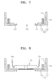
- FIG. 6 is a bottom plan view of a plastic case of the power system module illustrated in FIG. 1
- FIG. 7 is a cross-sectional view of the plastic case illustrated in FIG. 6 .
- the plastic case 110 includes the sidewall 112 and a floor 114 .
- the sidewall 112 is formed to extend vertically upward from the upper surface of the edge around the entire floor 114 .
- the floor 114 includes a through hole 115 formed therethrough, and the sidewall 112 includes a groove 113 .
- the groove 113 may be formed in oppositely facing surfaces of the sidewall 112 or may be formed in the entire perimeter of the sidewall 112 .
- the plastic case 110 may include polybutyleneterephtalate (PBT), polyphenynesulfide (PPS), or polypthalamide (PPA).
- the plastic case 110 may further include a fixing member 116 within for fixing the external terminal 140 ( FIG. 4 ).
- the fixing member 116 may be fixed vertically to the floor 114 by, for example, also forming the fixing member 116 when the plastic case 110 is formed.
- the plastic case 110 may further include a pair of auxiliary through holes 117 for aiding in fixing the power module package 120 ( FIG. 4 ) along with the through hole 115 .
- the plastic case 110 is not limited to the form illustrated in FIGS. 6 and 7 , and may adopt a variety of forms that fall within the scope of the present invention.
- the power module package 120 is fixed to a first region (i.e., the floor 114 ) inside the plastic case 110
- the control circuit board 130 is fixed to a second region (i.e., the sidewall 112 ) inside the plastic case 110
- the power module package 120 may be formed so that the heat sink 122 is exposed through the through hole 115 (in FIG. 7 ) of the floor 114 .
- the wall portion 124 passes and is exposed through the auxiliary through hole 117 (in FIG. 7 ) so that the power module package 120 can be more reliably fixed to the plastic case 110 .
- the control circuit board 130 may be inserted into the groove 113 (in FIG. 7 ) of the sidewall 114 .
- the control circuit board 130 according to another embodiment of the present invention may be attached to the plastic case 110 using another method.
- a fixing plate (not shown) may be attached to the sidewall 114 , and the control circuit board 130 may be supported on the fixing plate. That is, the fixing of the control circuit board 130 may be fixed through various means according to the shape of the plastic case 110 .
- At least one lead 126 of the power module package 120 is electrically connected to the control circuit board 130 .
- the lead 126 of the power module package 120 may be disposed to pass through the first hole 132 ( FIG. 5 ) of the control circuit board 130 and electrically connected to the control circuit board 130 using conductive solder (not shown).
- the lead 126 of the power module package 120 may be connected to the control circuit board 130 by alternative means.
- the lead 126 of the power module package 120 may simply contact the control circuit board 130 fixed to the control circuit board using conductive solder to electrically connect the two parts at the same time.
- the connecting of the lead 126 of the power module package 120 and the control circuit board 130 may be controlled, and the power module package 120 and the control circuit board 130 may be formed in a desired circuit configuration according to a desired power system.
- the external terminal 140 is disposed to pass through the second hole 134 ( FIG. 5 ) of the control circuit board 130 and is electrically connected to the control circuit board 130 by conductive solder. Accordingly, the external terminal 140 may be further fixed to the fixing member 116 of the plastic case 110 below the control circuit board 130 .
- the external terminal 140 for example, may be fixed to the plastic case 110 through a screw coupling inside the fixing member 116 .
- the external terminal 140 is directly connected to the control circuit board 130 , due to the fact that the control circuit board 130 is connected to the power module package 120 , the external terminal 140 can function as an output terminal for the entire system circuit of the power module package 120 and the control circuit board 130 . That is, the external terminal 140 performs the function of electrically connecting the power system module to an external device. Therefore, the number and position of the external terminal 140 may be adjusted according to the function of the power system module.
- the inside of the plastic case 110 may be filled with an insulating material which encloses the control circuit board 130 .
- the power module package 120 and the control circuit board 130 may be manufactured separately, and then fixed in a stacked format in the plastic case 110 . That is, the power module package 120 and the control circuit board 130 may be provided separately. Accordingly, a control circuit board 130 may be added to a power module package 120 according to a customer's requirements, in order to easily manufacture another power system module.
- the power module package 120 and the control circuit board 130 can be manufactured separately, the volume of the power module package 120 (having a relatively high manufacturing cost) can be reduced, thereby also reducing its manufacturing cost. Furthermore, because the power module package 120 and the control circuit board 130 can be stacked within a plastic case 110 , the circuit integration of both the power module package 120 and the control circuit board 130 can be increased, to obtain high integration of the power system module. Thus, the power system module according to embodiments of the present invention may be applied to products requiring highly integrated circuits, for example, automobiles.
- FIGS. 8 and 9 are cross-sectional views illustrating an manufacturing method of a power system module according to an embodiment of the present invention.
- a plastic case 110 defining a first region (for example, the floor 114 ) and a second region (for example, the sidewall 112 ) is provided.
- a detailed description of the plastic case 110 has already been given and is thus omitted below.
- a power module package 120 is fixed to the floor 114 of the plastic case 110 .
- the power module package 120 is first placed on the floor 114 , and is fixed to the floor 114 using an adhesive printing or dotting method.
- At least one lead 126 of the power module package 120 is disposed vertically upward from the floor 114 .
- a curing operation may be further implemented.
- the control circuit board 130 is fixed to the sidewall 112 of the plastic case 110 .
- the control circuit board 130 may be fixed to the plastic case 110 by inserting the edges of the control circuit board 130 in the groove 113 (in FIG. 7 ) of the sidewall 112 .
- the control circuit board 130 may be fixed using alternative methods. For example, a fixing or support plate may be placed on the sidewall 112 , and the control circuit board 130 may be installed on the fixing plate.
- the lead 126 of the power module package 120 is electrically connected to the control circuit board 130 .
- the lead 126 of the power module package 120 may be positioned to pass through the first hole 132 ( FIG. 5 ) of the control circuit board 130 and may be electrically connected to the control circuit board 130 using soldering.
- the leads 126 of the power module package 120 may be connected to the control circuit board 130 using alternative methods.
- the leads 126 may be first placed in contact with the control circuit board 130 and then electrically connected and fixed to the control circuit board 130 using soldering.
- At least one external terminal 140 is electrically connected to the control circuit board 130 .
- an external terminal 140 is positioned to pass through a second hole 134 (in FIG. 5 ) of the control circuit board 140 and is electrically connected to the control circuit board 130 using soldering.
- the external terminal 140 may be mechanically fixed to the plastic case 110 .
- the external terminal 140 may be screwed and coupled to a fixing member 116 at the bottom of the control circuit board 130 , in order to fix the external terminal 140 to the plastic case 110 .
- the above-described manufacturing method allows the power module package 120 and the control circuit board 130 to be separately manufactured, in order to easily satisfy customers' demands. Moreover, this method of separately manufacturing the components can increase circuit integration of the power system module. Also, the power module package 120 (having a relatively expensive manufacturing cost) does not require a built-in control device, so that manufacturing costs can be lowered in the above-described manufacturing method.
Abstract
Description
Claims (17)
Priority Applications (1)
| Application Number | Priority Date | Filing Date | Title |
|---|---|---|---|
| US12/722,153 US7986531B2 (en) | 2006-04-20 | 2010-03-11 | Power system module and method of fabricating the same |
Applications Claiming Priority (4)
| Application Number | Priority Date | Filing Date | Title |
|---|---|---|---|
| KR1020060035770A KR101203466B1 (en) | 2006-04-20 | 2006-04-20 | Power system module and method for fabricating the same |
| KR10-2006-0035770 | 2006-04-20 | ||
| US11/696,801 US7706146B2 (en) | 2006-04-20 | 2007-04-05 | Power system module and method of fabricating the same |
| US12/722,153 US7986531B2 (en) | 2006-04-20 | 2010-03-11 | Power system module and method of fabricating the same |
Related Parent Applications (1)
| Application Number | Title | Priority Date | Filing Date |
|---|---|---|---|
| US11/696,801 Continuation US7706146B2 (en) | 2006-04-20 | 2007-04-05 | Power system module and method of fabricating the same |
Publications (2)
| Publication Number | Publication Date |
|---|---|
| US20100165576A1 US20100165576A1 (en) | 2010-07-01 |
| US7986531B2 true US7986531B2 (en) | 2011-07-26 |
Family
ID=38818080
Family Applications (2)
| Application Number | Title | Priority Date | Filing Date |
|---|---|---|---|
| US11/696,801 Active 2028-03-06 US7706146B2 (en) | 2006-04-20 | 2007-04-05 | Power system module and method of fabricating the same |
| US12/722,153 Active US7986531B2 (en) | 2006-04-20 | 2010-03-11 | Power system module and method of fabricating the same |
Family Applications Before (1)
| Application Number | Title | Priority Date | Filing Date |
|---|---|---|---|
| US11/696,801 Active 2028-03-06 US7706146B2 (en) | 2006-04-20 | 2007-04-05 | Power system module and method of fabricating the same |
Country Status (2)
| Country | Link |
|---|---|
| US (2) | US7706146B2 (en) |
| KR (1) | KR101203466B1 (en) |
Cited By (3)
| Publication number | Priority date | Publication date | Assignee | Title |
|---|---|---|---|---|
| US20110299253A1 (en) * | 2010-06-02 | 2011-12-08 | Vincotech Holdings S.A.R.L. | Electrical power module and method for connecting an electrical power module to a printed circuit board and a heat sink |
| US8604610B1 (en) | 2012-06-13 | 2013-12-10 | Fairchild Semiconductor Corporation | Flexible power module semiconductor packages |
| US20140231975A1 (en) * | 2013-02-15 | 2014-08-21 | Fuji Electric Co., Ltd. | Semiconductor device |
Families Citing this family (30)
| Publication number | Priority date | Publication date | Assignee | Title |
|---|---|---|---|---|
| KR101203466B1 (en) * | 2006-04-20 | 2012-11-21 | 페어차일드코리아반도체 주식회사 | Power system module and method for fabricating the same |
| JP4934559B2 (en) * | 2007-09-27 | 2012-05-16 | オンセミコンダクター・トレーディング・リミテッド | Circuit device and manufacturing method thereof |
| JP4969388B2 (en) * | 2007-09-27 | 2012-07-04 | オンセミコンダクター・トレーディング・リミテッド | Circuit module |
| TWI402952B (en) * | 2007-09-27 | 2013-07-21 | Sanyo Electric Co | Circuit device and manufacturing method thereof |
| JP2009081325A (en) * | 2007-09-27 | 2009-04-16 | Sanyo Electric Co Ltd | Circuit device |
| KR101524545B1 (en) * | 2008-02-28 | 2015-06-01 | 페어차일드코리아반도체 주식회사 | Power device package and the method of fabricating the same |
| KR101519062B1 (en) * | 2008-03-31 | 2015-05-11 | 페어차일드코리아반도체 주식회사 | Semiconductor Device Package |
| US7952204B2 (en) * | 2008-04-14 | 2011-05-31 | Fairchild Semiconductor Corporation | Semiconductor die packages with multiple integrated substrates, systems using the same, and methods using the same |
| JP5586866B2 (en) * | 2008-09-29 | 2014-09-10 | 株式会社日立産機システム | Power converter |
| KR101321282B1 (en) * | 2011-06-17 | 2013-10-28 | 삼성전기주식회사 | Power module package and system module having the same |
| FR2979177B1 (en) * | 2011-08-19 | 2014-05-23 | Valeo Sys Controle Moteur Sas | POWER BLOCK FOR ELECTRIC VEHICLE INVERTER |
| JP5859906B2 (en) * | 2012-04-20 | 2016-02-16 | 三菱電機株式会社 | Semiconductor device and manufacturing method of semiconductor device |
| CN103515340B (en) * | 2012-06-29 | 2016-09-07 | 三星电机株式会社 | Power module encapsulation and the method being used for manufacturing power module encapsulation |
| CN103515364A (en) * | 2012-06-29 | 2014-01-15 | 三星电机株式会社 | Power module package and method for manufacturing the same |
| KR101443972B1 (en) * | 2012-10-31 | 2014-09-23 | 삼성전기주식회사 | All-in-one power semiconductor module |
| US20140167237A1 (en) * | 2012-12-14 | 2014-06-19 | Samsung Electro-Mechanics Co., Ltd. | Power module package |
| KR101502669B1 (en) * | 2012-12-14 | 2015-03-13 | 삼성전기주식회사 | Power module package and method for manufacturing the same |
| JP6119313B2 (en) | 2013-03-08 | 2017-04-26 | 富士電機株式会社 | Semiconductor device |
| JP6083334B2 (en) * | 2013-06-25 | 2017-02-22 | 株式会社デンソー | Electronic equipment |
| US9018753B2 (en) * | 2013-08-02 | 2015-04-28 | Stmicroelectronics Pte Ltd | Electronic modules |
| US9497570B2 (en) | 2014-02-06 | 2016-11-15 | Nimbelink Corp. | Embedded wireless modem |
| USD731491S1 (en) * | 2014-02-07 | 2015-06-09 | NimbeLink L.L.C. | Embedded cellular modem |
| CN106340513B (en) * | 2015-07-09 | 2019-03-15 | 台达电子工业股份有限公司 | A kind of power module of integral control circuit |
| US9645425B2 (en) * | 2015-07-27 | 2017-05-09 | Shenzhen China Star Optoelectronics Technology Co., Ltd | Driving circuit board fixing structure and liquid crystal display device |
| US10057989B1 (en) * | 2017-04-10 | 2018-08-21 | Tactotek Oy | Multilayer structure and related method of manufacture for electronics |
| FR3074011B1 (en) * | 2017-11-21 | 2019-12-20 | Safran Electronics & Defense | ELECTRIC POWER MODULE |
| FR3084557B1 (en) * | 2018-07-30 | 2020-07-31 | Safran Electrical & Power | ELECTRICAL CONTROL DEVICE |
| TWI762765B (en) * | 2019-02-20 | 2022-05-01 | 台達電子工業股份有限公司 | Package structure of power module |
| JP7170593B2 (en) * | 2019-06-21 | 2022-11-14 | 日立Astemo株式会社 | power converter |
| TWI792659B (en) * | 2021-11-04 | 2023-02-11 | 新加坡商光寶科技新加坡私人有限公司 | Power module |
Citations (13)
| Publication number | Priority date | Publication date | Assignee | Title |
|---|---|---|---|---|
| US5513072A (en) | 1993-11-18 | 1996-04-30 | Kabushiki Kaisha Toshiba | Power module using IMS as heat spreader |
| US5519252A (en) | 1992-07-24 | 1996-05-21 | Fuji Electric Co., Ltd. | Power semiconductor device employing pin block connection arrangement for facilitated and economized manufacture |
| US5543586A (en) | 1994-03-11 | 1996-08-06 | The Panda Project | Apparatus having inner layers supporting surface-mount components |
| US6005773A (en) | 1996-12-23 | 1999-12-21 | Lucent Technologies Inc. | Board-mountable power supply module |
| US6060772A (en) | 1997-06-30 | 2000-05-09 | Kabushiki Kaisha Toshiba | Power semiconductor module with a plurality of semiconductor chips |
| US6144571A (en) | 1999-02-22 | 2000-11-07 | Hitachi, Ltd. | Semiconductor module, power converter using the same and manufacturing method thereof |
| US6421244B1 (en) | 1999-12-28 | 2002-07-16 | Mitsubishi Denki Kabushiki Kaisha | Power module |
| US6521983B1 (en) | 2000-08-29 | 2003-02-18 | Mitsubishi Denki Kabushiki Kaisha | Semiconductor device for electric power |
| US6600653B2 (en) | 2001-04-19 | 2003-07-29 | Keihin Corporation | Electronic vehicle control unit |
| US20040227476A1 (en) | 2002-12-19 | 2004-11-18 | International Rectifier Corp. | Flexible inverter power module for motor drives |
| US6995461B2 (en) | 2001-07-23 | 2006-02-07 | Fuji Electric Co., Ltd. | Semiconductor device |
| US7208833B2 (en) | 2001-01-17 | 2007-04-24 | Matsushita Electric Industrial Co., Ltd. | Electronic circuit device having circuit board electrically connected to semiconductor element via metallic plate |
| US7706146B2 (en) * | 2006-04-20 | 2010-04-27 | Fairchild Korea Semiconductor Ltd | Power system module and method of fabricating the same |
Family Cites Families (3)
| Publication number | Priority date | Publication date | Assignee | Title |
|---|---|---|---|---|
| JP3516789B2 (en) * | 1995-11-15 | 2004-04-05 | 三菱電機株式会社 | Semiconductor power module |
| JP3410969B2 (en) * | 1997-06-30 | 2003-05-26 | 株式会社東芝 | Semiconductor device |
| JP2003298009A (en) * | 2002-03-29 | 2003-10-17 | Toshiba Corp | Power module and power converter using the same |
-
2006
- 2006-04-20 KR KR1020060035770A patent/KR101203466B1/en not_active IP Right Cessation
-
2007
- 2007-04-05 US US11/696,801 patent/US7706146B2/en active Active
-
2010
- 2010-03-11 US US12/722,153 patent/US7986531B2/en active Active
Patent Citations (13)
| Publication number | Priority date | Publication date | Assignee | Title |
|---|---|---|---|---|
| US5519252A (en) | 1992-07-24 | 1996-05-21 | Fuji Electric Co., Ltd. | Power semiconductor device employing pin block connection arrangement for facilitated and economized manufacture |
| US5513072A (en) | 1993-11-18 | 1996-04-30 | Kabushiki Kaisha Toshiba | Power module using IMS as heat spreader |
| US5543586A (en) | 1994-03-11 | 1996-08-06 | The Panda Project | Apparatus having inner layers supporting surface-mount components |
| US6005773A (en) | 1996-12-23 | 1999-12-21 | Lucent Technologies Inc. | Board-mountable power supply module |
| US6060772A (en) | 1997-06-30 | 2000-05-09 | Kabushiki Kaisha Toshiba | Power semiconductor module with a plurality of semiconductor chips |
| US6144571A (en) | 1999-02-22 | 2000-11-07 | Hitachi, Ltd. | Semiconductor module, power converter using the same and manufacturing method thereof |
| US6421244B1 (en) | 1999-12-28 | 2002-07-16 | Mitsubishi Denki Kabushiki Kaisha | Power module |
| US6521983B1 (en) | 2000-08-29 | 2003-02-18 | Mitsubishi Denki Kabushiki Kaisha | Semiconductor device for electric power |
| US7208833B2 (en) | 2001-01-17 | 2007-04-24 | Matsushita Electric Industrial Co., Ltd. | Electronic circuit device having circuit board electrically connected to semiconductor element via metallic plate |
| US6600653B2 (en) | 2001-04-19 | 2003-07-29 | Keihin Corporation | Electronic vehicle control unit |
| US6995461B2 (en) | 2001-07-23 | 2006-02-07 | Fuji Electric Co., Ltd. | Semiconductor device |
| US20040227476A1 (en) | 2002-12-19 | 2004-11-18 | International Rectifier Corp. | Flexible inverter power module for motor drives |
| US7706146B2 (en) * | 2006-04-20 | 2010-04-27 | Fairchild Korea Semiconductor Ltd | Power system module and method of fabricating the same |
Cited By (4)
| Publication number | Priority date | Publication date | Assignee | Title |
|---|---|---|---|---|
| US20110299253A1 (en) * | 2010-06-02 | 2011-12-08 | Vincotech Holdings S.A.R.L. | Electrical power module and method for connecting an electrical power module to a printed circuit board and a heat sink |
| US8604610B1 (en) | 2012-06-13 | 2013-12-10 | Fairchild Semiconductor Corporation | Flexible power module semiconductor packages |
| US20140231975A1 (en) * | 2013-02-15 | 2014-08-21 | Fuji Electric Co., Ltd. | Semiconductor device |
| US9064818B2 (en) * | 2013-02-15 | 2015-06-23 | Fuji Electric Co., Ltd. | Semiconductor device |
Also Published As
| Publication number | Publication date |
|---|---|
| KR101203466B1 (en) | 2012-11-21 |
| US20070284947A1 (en) | 2007-12-13 |
| KR20070103876A (en) | 2007-10-25 |
| US7706146B2 (en) | 2010-04-27 |
| US20100165576A1 (en) | 2010-07-01 |
Similar Documents
| Publication | Publication Date | Title |
|---|---|---|
| US7986531B2 (en) | Power system module and method of fabricating the same | |
| KR101505552B1 (en) | Complex semiconductor package and method of fabricating the same | |
| US8107255B2 (en) | Circuit device and method of manufacturing the same | |
| US6777819B2 (en) | Semiconductor package with flash-proof device | |
| US11615967B2 (en) | Power module package and method of manufacturing the same | |
| US9472541B2 (en) | Methods for manufacturing an electronic module | |
| US9795053B2 (en) | Electronic device and method for manufacturing the electronic device | |
| JP6119313B2 (en) | Semiconductor device | |
| US10109544B2 (en) | Baseplate for an electronic module | |
| JP4208490B2 (en) | Semiconductor power module and manufacturing method thereof | |
| US6905361B2 (en) | Electrical device | |
| JP2001085613A (en) | Transfer mold power module | |
| KR100706505B1 (en) | Semiconductor package | |
| US10366906B2 (en) | Electronic package and its package substrate | |
| KR20150061441A (en) | Package Substrate and Manufacturing Method for the same and Power module Package using the same | |
| JPH0655971A (en) | Electronic direction indicator | |
| JP3021070U (en) | Semiconductor device | |
| KR100325669B1 (en) | Semiconductor package | |
| KR102561986B1 (en) | Semi-conductor package | |
| KR20160100861A (en) | Housing for power module package and a method thereof | |
| JPH05292744A (en) | Mounting structure for power supply module | |
| KR101464984B1 (en) | Intelligent power module with compaction size standardized | |
| KR20160111831A (en) | Power module package | |
| JP2005310981A (en) | Power module |
Legal Events
| Date | Code | Title | Description |
|---|---|---|---|
| FEPP | Fee payment procedure |
Free format text: PAYOR NUMBER ASSIGNED (ORIGINAL EVENT CODE: ASPN); ENTITY STATUS OF PATENT OWNER: LARGE ENTITY |
|
| STCF | Information on status: patent grant |
Free format text: PATENTED CASE |
|
| FPAY | Fee payment |
Year of fee payment: 4 |
|
| AS | Assignment |
Owner name: SEMICONDUCTOR COMPONENTS INDUSTRIES, LLC, ARIZONA Free format text: ASSIGNMENT OF ASSIGNORS INTEREST;ASSIGNOR:FAIRCHILD KOREA SEMICONDUCTOR, LTD.;REEL/FRAME:044361/0205 Effective date: 20171102 |
|
| AS | Assignment |
Owner name: DEUTSCHE BANK AG NEW YORK BRANCH, AS COLLATERAL AGENT, NEW YORK Free format text: PATENT SECURITY AGREEMENT;ASSIGNORS:SEMICONDUCTOR COMPONENTS INDUSTRIES, LLC;FAIRCHILD SEMICONDUCTOR CORPORATION;REEL/FRAME:044481/0541 Effective date: 20170504 Owner name: DEUTSCHE BANK AG NEW YORK BRANCH, AS COLLATERAL AG Free format text: PATENT SECURITY AGREEMENT;ASSIGNORS:SEMICONDUCTOR COMPONENTS INDUSTRIES, LLC;FAIRCHILD SEMICONDUCTOR CORPORATION;REEL/FRAME:044481/0541 Effective date: 20170504 |
|
| MAFP | Maintenance fee payment |
Free format text: PAYMENT OF MAINTENANCE FEE, 8TH YEAR, LARGE ENTITY (ORIGINAL EVENT CODE: M1552); ENTITY STATUS OF PATENT OWNER: LARGE ENTITY Year of fee payment: 8 |
|
| MAFP | Maintenance fee payment |
Free format text: PAYMENT OF MAINTENANCE FEE, 12TH YEAR, LARGE ENTITY (ORIGINAL EVENT CODE: M1553); ENTITY STATUS OF PATENT OWNER: LARGE ENTITY Year of fee payment: 12 |
|
| AS | Assignment |
Owner name: FAIRCHILD SEMICONDUCTOR CORPORATION, ARIZONA Free format text: RELEASE OF SECURITY INTEREST IN PATENTS RECORDED AT REEL 04481, FRAME 0541;ASSIGNOR:DEUTSCHE BANK AG NEW YORK BRANCH, AS COLLATERAL AGENT;REEL/FRAME:064072/0459 Effective date: 20230622 Owner name: SEMICONDUCTOR COMPONENTS INDUSTRIES, LLC, ARIZONA Free format text: RELEASE OF SECURITY INTEREST IN PATENTS RECORDED AT REEL 04481, FRAME 0541;ASSIGNOR:DEUTSCHE BANK AG NEW YORK BRANCH, AS COLLATERAL AGENT;REEL/FRAME:064072/0459 Effective date: 20230622 |