US8002946B2 - Mask etch plasma reactor with cathode providing a uniform distribution of etch rate - Google Patents
Mask etch plasma reactor with cathode providing a uniform distribution of etch rate Download PDFInfo
- Publication number
- US8002946B2 US8002946B2 US11/589,337 US58933706A US8002946B2 US 8002946 B2 US8002946 B2 US 8002946B2 US 58933706 A US58933706 A US 58933706A US 8002946 B2 US8002946 B2 US 8002946B2
- Authority
- US
- United States
- Prior art keywords
- cathode
- mask
- rectangular
- etch
- metal
- Prior art date
- Legal status (The legal status is an assumption and is not a legal conclusion. Google has not performed a legal analysis and makes no representation as to the accuracy of the status listed.)
- Active, expires
Links
Images
Classifications
-
- H—ELECTRICITY
- H01—ELECTRIC ELEMENTS
- H01L—SEMICONDUCTOR DEVICES NOT COVERED BY CLASS H10
- H01L21/00—Processes or apparatus adapted for the manufacture or treatment of semiconductor or solid state devices or of parts thereof
- H01L21/02—Manufacture or treatment of semiconductor devices or of parts thereof
- H01L21/04—Manufacture or treatment of semiconductor devices or of parts thereof the devices having at least one potential-jump barrier or surface barrier, e.g. PN junction, depletion layer or carrier concentration layer
- H01L21/18—Manufacture or treatment of semiconductor devices or of parts thereof the devices having at least one potential-jump barrier or surface barrier, e.g. PN junction, depletion layer or carrier concentration layer the devices having semiconductor bodies comprising elements of Group IV of the Periodic System or AIIIBV compounds with or without impurities, e.g. doping materials
- H01L21/30—Treatment of semiconductor bodies using processes or apparatus not provided for in groups H01L21/20 - H01L21/26
- H01L21/302—Treatment of semiconductor bodies using processes or apparatus not provided for in groups H01L21/20 - H01L21/26 to change their surface-physical characteristics or shape, e.g. etching, polishing, cutting
- H01L21/306—Chemical or electrical treatment, e.g. electrolytic etching
- H01L21/3065—Plasma etching; Reactive-ion etching
-
- H—ELECTRICITY
- H01—ELECTRIC ELEMENTS
- H01L—SEMICONDUCTOR DEVICES NOT COVERED BY CLASS H10
- H01L21/00—Processes or apparatus adapted for the manufacture or treatment of semiconductor or solid state devices or of parts thereof
- H01L21/67—Apparatus specially adapted for handling semiconductor or electric solid state devices during manufacture or treatment thereof; Apparatus specially adapted for handling wafers during manufacture or treatment of semiconductor or electric solid state devices or components ; Apparatus not specifically provided for elsewhere
- H01L21/67005—Apparatus not specifically provided for elsewhere
- H01L21/67011—Apparatus for manufacture or treatment
- H01L21/67017—Apparatus for fluid treatment
- H01L21/67063—Apparatus for fluid treatment for etching
- H01L21/67069—Apparatus for fluid treatment for etching for drying etching
-
- H—ELECTRICITY
- H01—ELECTRIC ELEMENTS
- H01J—ELECTRIC DISCHARGE TUBES OR DISCHARGE LAMPS
- H01J37/00—Discharge tubes with provision for introducing objects or material to be exposed to the discharge, e.g. for the purpose of examination or processing thereof
- H01J37/32—Gas-filled discharge tubes
- H01J37/32431—Constructional details of the reactor
- H01J37/32532—Electrodes
- H01J37/3255—Material
-
- H—ELECTRICITY
- H01—ELECTRIC ELEMENTS
- H01L—SEMICONDUCTOR DEVICES NOT COVERED BY CLASS H10
- H01L21/00—Processes or apparatus adapted for the manufacture or treatment of semiconductor or solid state devices or of parts thereof
- H01L21/67—Apparatus specially adapted for handling semiconductor or electric solid state devices during manufacture or treatment thereof; Apparatus specially adapted for handling wafers during manufacture or treatment of semiconductor or electric solid state devices or components ; Apparatus not specifically provided for elsewhere
- H01L21/67005—Apparatus not specifically provided for elsewhere
- H01L21/67242—Apparatus for monitoring, sorting or marking
- H01L21/67253—Process monitoring, e.g. flow or thickness monitoring
-
- H—ELECTRICITY
- H01—ELECTRIC ELEMENTS
- H01L—SEMICONDUCTOR DEVICES NOT COVERED BY CLASS H10
- H01L21/00—Processes or apparatus adapted for the manufacture or treatment of semiconductor or solid state devices or of parts thereof
- H01L21/67—Apparatus specially adapted for handling semiconductor or electric solid state devices during manufacture or treatment thereof; Apparatus specially adapted for handling wafers during manufacture or treatment of semiconductor or electric solid state devices or components ; Apparatus not specifically provided for elsewhere
- H01L21/683—Apparatus specially adapted for handling semiconductor or electric solid state devices during manufacture or treatment thereof; Apparatus specially adapted for handling wafers during manufacture or treatment of semiconductor or electric solid state devices or components ; Apparatus not specifically provided for elsewhere for supporting or gripping
- H01L21/687—Apparatus specially adapted for handling semiconductor or electric solid state devices during manufacture or treatment thereof; Apparatus specially adapted for handling wafers during manufacture or treatment of semiconductor or electric solid state devices or components ; Apparatus not specifically provided for elsewhere for supporting or gripping using mechanical means, e.g. chucks, clamps or pinches
- H01L21/68714—Apparatus specially adapted for handling semiconductor or electric solid state devices during manufacture or treatment thereof; Apparatus specially adapted for handling wafers during manufacture or treatment of semiconductor or electric solid state devices or components ; Apparatus not specifically provided for elsewhere for supporting or gripping using mechanical means, e.g. chucks, clamps or pinches the wafers being placed on a susceptor, stage or support
- H01L21/68742—Apparatus specially adapted for handling semiconductor or electric solid state devices during manufacture or treatment thereof; Apparatus specially adapted for handling wafers during manufacture or treatment of semiconductor or electric solid state devices or components ; Apparatus not specifically provided for elsewhere for supporting or gripping using mechanical means, e.g. chucks, clamps or pinches the wafers being placed on a susceptor, stage or support characterised by a lifting arrangement, e.g. lift pins
-
- H—ELECTRICITY
- H01—ELECTRIC ELEMENTS
- H01L—SEMICONDUCTOR DEVICES NOT COVERED BY CLASS H10
- H01L21/00—Processes or apparatus adapted for the manufacture or treatment of semiconductor or solid state devices or of parts thereof
- H01L21/67—Apparatus specially adapted for handling semiconductor or electric solid state devices during manufacture or treatment thereof; Apparatus specially adapted for handling wafers during manufacture or treatment of semiconductor or electric solid state devices or components ; Apparatus not specifically provided for elsewhere
- H01L21/683—Apparatus specially adapted for handling semiconductor or electric solid state devices during manufacture or treatment thereof; Apparatus specially adapted for handling wafers during manufacture or treatment of semiconductor or electric solid state devices or components ; Apparatus not specifically provided for elsewhere for supporting or gripping
- H01L21/687—Apparatus specially adapted for handling semiconductor or electric solid state devices during manufacture or treatment thereof; Apparatus specially adapted for handling wafers during manufacture or treatment of semiconductor or electric solid state devices or components ; Apparatus not specifically provided for elsewhere for supporting or gripping using mechanical means, e.g. chucks, clamps or pinches
- H01L21/68714—Apparatus specially adapted for handling semiconductor or electric solid state devices during manufacture or treatment thereof; Apparatus specially adapted for handling wafers during manufacture or treatment of semiconductor or electric solid state devices or components ; Apparatus not specifically provided for elsewhere for supporting or gripping using mechanical means, e.g. chucks, clamps or pinches the wafers being placed on a susceptor, stage or support
- H01L21/68757—Apparatus specially adapted for handling semiconductor or electric solid state devices during manufacture or treatment thereof; Apparatus specially adapted for handling wafers during manufacture or treatment of semiconductor or electric solid state devices or components ; Apparatus not specifically provided for elsewhere for supporting or gripping using mechanical means, e.g. chucks, clamps or pinches the wafers being placed on a susceptor, stage or support characterised by a coating or a hardness or a material
-
- H—ELECTRICITY
- H01—ELECTRIC ELEMENTS
- H01L—SEMICONDUCTOR DEVICES NOT COVERED BY CLASS H10
- H01L21/00—Processes or apparatus adapted for the manufacture or treatment of semiconductor or solid state devices or of parts thereof
- H01L21/67—Apparatus specially adapted for handling semiconductor or electric solid state devices during manufacture or treatment thereof; Apparatus specially adapted for handling wafers during manufacture or treatment of semiconductor or electric solid state devices or components ; Apparatus not specifically provided for elsewhere
- H01L21/683—Apparatus specially adapted for handling semiconductor or electric solid state devices during manufacture or treatment thereof; Apparatus specially adapted for handling wafers during manufacture or treatment of semiconductor or electric solid state devices or components ; Apparatus not specifically provided for elsewhere for supporting or gripping
- H01L21/687—Apparatus specially adapted for handling semiconductor or electric solid state devices during manufacture or treatment thereof; Apparatus specially adapted for handling wafers during manufacture or treatment of semiconductor or electric solid state devices or components ; Apparatus not specifically provided for elsewhere for supporting or gripping using mechanical means, e.g. chucks, clamps or pinches
- H01L21/68714—Apparatus specially adapted for handling semiconductor or electric solid state devices during manufacture or treatment thereof; Apparatus specially adapted for handling wafers during manufacture or treatment of semiconductor or electric solid state devices or components ; Apparatus not specifically provided for elsewhere for supporting or gripping using mechanical means, e.g. chucks, clamps or pinches the wafers being placed on a susceptor, stage or support
- H01L21/68785—Apparatus specially adapted for handling semiconductor or electric solid state devices during manufacture or treatment thereof; Apparatus specially adapted for handling wafers during manufacture or treatment of semiconductor or electric solid state devices or components ; Apparatus not specifically provided for elsewhere for supporting or gripping using mechanical means, e.g. chucks, clamps or pinches the wafers being placed on a susceptor, stage or support characterised by the mechanical construction of the susceptor, stage or support
Definitions
- a single mask pattern generally occupies a four inch square area on a quartz mask.
- the image of the mask pattern is focused down to the area of a single die (a one inch square) on the wafer and is then stepped across the wafer, forming a single image for each die.
- the mask pattern Prior to etching the mask pattern into the quartz mask, the mask pattern is written in photoresist by a scanning electron beam, a time consuming process which makes the cost of the mask very high.
- the mask etch process is not uniform across the surface of the mask.
- the e-beam written photoresist pattern is itself non-uniform, and exhibits, in the case of 45 nm feature sizes on the wafer, as much as 2-3 nm variation in critical dimension (e.g., line width) across the entire mask. (This variation is the 3 ⁇ variance of all measured line widths, for example.)
- critical dimension e.g., line width
- Such non-uniformities in photoresist critical dimension typically varies among different mask sources or customers.
- the mask etch process must not increase this variation by more than 1 nm, so that the variation in the etched mask pattern cannot exceed 3-4 nm.
- each line is defined by a chrome line with thin quartz lines exposed on each side of the chrome line, the quartz line on one side being etched to a precise depth that provides a 180 degree phase shift of the light relative to light passing through the un-etched quartz line on the other side of the chrome line.
- the etch process In order to precisely control the etch depth in the quartz, the etch process must be closely monitored by periodically interrupting it to measure the etch depth in the quartz.
- Each such inspection requires removing the mask from the mask etch reactor chamber, removing the photoresist, measuring the etch depth and then estimating the etch process time remaining to reach the target depth based upon the elapsed etch process time, depositing new photoresist, e-beam writing the mask pattern on the resist, re-introducing the mask into the mask etch chamber and restarting the etch process.
- the estimate of remaining etch time to reach the desired depth assumes that the etch rate remains stable and uniform, and therefore is an unreliable estimate.
- the problems of such a cumbersome procedure include low productivity and high cost as well as increased opportunity for introduction of contamination or faults in the photoresist pattern. However, because of the requirement for an accurately controlled etch depth, there has seemed to be no way around such problems.
- etch rate distribution can be reduced to some extent by employing a source power applicator that can vary the radial distribution of the plasma ion density, such as an inductive source power applicator consisting of inner and outer coil antennas overlying the wafer.
- a source power applicator that can vary the radial distribution of the plasma ion density, such as an inductive source power applicator consisting of inner and outer coil antennas overlying the wafer.
- non-uniformities in etch rate distribution can be non-symmetrical, such as a high etch rate in one corner of the mask, for example.
- a more fundamental limitation is that the mask etch process tends to have such an extremely center-low distribution of etch rate that a tunable feature, such an inductive power applicator having inner and outer coils, is incapable of transforming the etch rate distribution out of the center-low regime.
- etch rate distribution tends to vary widely among different reactors of the same design and can vary widely within the same reactor whenever a key part or a consumable component is replaced, such as replacement of the cathode.
- the etch rate distribution appears to be highly sensitive to small variations in features of the replaced part, with unpredictable changes upon consumable replacement.
- a plasma reactor for etching a workpiece such as a rectangular or square mask includes a vacuum chamber having a ceiling and a sidewall and a workpiece support pedestal within the chamber including a cathode having a surface for supporting a workpiece.
- the surface comprises plural respective zones, each being formed of respective materials of different electrical characteristics.
- the zones can be arranged concentrically relative to an axis of symmetry of the wafer support pedestal.
- an inner zone comprises a conductor material and an annular outer zone comprises an insulator.
- the zones are of different insulator materials of different electrical permittivities.
- the cathode and an underlying facilities plate are formed of a metal.
- the cathode has a bottom surface and the facilities plate has a top surface facing the bottom surface of the cathode, and they are fastened together by screws of a dissimilar metal.
- a thin ring layer is provided between the cathode and the facilities plate formed of the dissimilar metal and being located at the periphery of the cathode and facilities plate.
- a highly conductive coating is provided on the periphery of facing surfaces of the cathode and plate.
- FIG. 1 depicts a plasma reactor for carrying out a mask etch process.
- FIG. 2A depicts a lower portion of the reactor of FIG. 1 .
- FIG. 2B illustrates a mask support pedestal of the reactor of FIG. 1 in a raised position.
- FIG. 3 is a top view of a cathode of the reactor of FIG. 1 .
- FIGS. 4 and 5 are top and side views of one alternative embodiment of the cathode.
- FIGS. 6 and 7 are top and side views of another alternative embodiment of the cathode.
- FIG. 8 is a simplified diagram of a plasma reactor having a backside end point detection apparatus.
- FIGS. 9 and 10 are graphs of an optical end point detection signal obtained from the front side and back side, respectively, of the mask.
- FIGS. 11 and 12 are graphs of an interference fringe optical signal obtained from the front side and back side, respectively, of the mask.
- FIG. 13 is a graph of a multiple wavelength interference spectrum signal obtained in one embodiment of the reactor of FIG. 8 .
- FIG. 14 illustrates an embodiment of the reactor of FIG. 8 with backside end point detection based upon overall reflected light intensity, corresponding to FIG. 10 .
- FIG. 15 illustrates an embodiment of the reactor of FIG. 8 with backside endpoint detection based upon interference fringe counting, corresponding to FIG. 12 .
- FIG. 16 illustrates an embodiment of the reactor of FIG. 8 with backside endpoint detection based upon multiple wavelength interference spectrometry.
- FIG. 17 illustrates an embodiment of the reactor of FIG. 8 with backside endpoint detection based upon optical emission spectrometry (OES).
- OES optical emission spectrometry
- FIG. 18 illustrates a working example having both OES and interference-based backside endpoint detection.
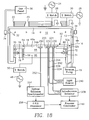
- FIGS. 19 and 20 are perspective view of the cathode and facilities plate, respectively, of the embodiment of FIG. 18 .
- FIG. 21 is a cross-sectional view of the cathode of FIG. 19 .
- FIGS. 22A and 22B depict a sequence of steps in a quartz mask etch process employing backside endpoint detection.
- FIGS. 23A , 23 B, 23 C, 23 D and 23 E depict a sequence of steps in a chrome-molysilicide-quartz mask etch process employing backside endpoint detection.
- FIGS. 24A , 24 B, 24 C, 24 D and 24 E depict a sequence of steps in a chrome-quartz mask etch process employing backside endpoint detection.
- FIGS. 25 and 26 are side and top views, respectively, of an embodiment in which real time etch rate distribution is continuously measured from the mask backside.
- RF bias power is applied to the pedestal to control plasma ion energy at the mask surface
- RF source power is applied to an overhead coil antenna, for example, to generate plasma ions.
- the RF bias power controls the electric field at the mask surface that affects the ion energy. Since the ion energy at the mask surface affects the etch rate, RF electrical non-uniformities in the pedestal create non-uniformities in the distribution of etch rate across the mask surface.
- the conduction around this perimeter can be non-uniform due to a number of factors, such as uneven tightening of the titanium screws and/or surface finish variations around the perimeter of either the plate or the pedestal.
- We have solved these problems by the introduction of several features that enhance RF electrical uniformity across the pedestal.
- the non-uniformities or discontinuities in the RF field arising from the presence of the titanium screws in the aluminum cathode are addressed by providing a continuous titanium ring extending around the perimeter of the top surface of the cathode that encompasses the heads of all the titanium screws.
- Variations in conductivity due surface differences or uneven tightening of the titanium screws are addressed by providing highly conductive nickel plating on the facing perimeter surfaces of the facilities plate and the cathode, and by the introduction of an RF gasket between the facilities plate and the cathode that is compressed between them at their perimeter.
- a plasma reactor for etching patterns in a mask includes a vacuum chamber 10 enclosed by a side wall 12 and an overlying ceiling 14 and is evacuated by a vacuum pump 15 that controls chamber pressure.
- a mask support pedestal 16 inside the chamber 10 supports a mask 18 .
- the mask typically consists of a quartz substrate and can further include additional mask thin film layers on the top surface of the quartz substrate, such as chrome and molybdenum silicide.
- a pattern-defining layer is present, which may be photoresist or a hardmask formed of the chrome layer.
- the quartz substrate has no overlying layers except for the photoresist pattern.
- Plasma source power is applied by overlying inner and outer coil antennas 20 , 22 driven by respective RF source power generators 24 , 26 through respective RF impedance match circuits 28 , 30 .
- the sidewall 12 may be aluminum or other metal coupled to ground
- the ceiling 14 is typically an insulating material that permits inductive coupling of RF power from the coil antennas 20 , 22 into the chamber 10 .
- Process gas is introduced through evenly spaced injection nozzles 32 in the top of the side wall 12 through a gas manifold 34 from a gas panel 36 .
- the gas panel 36 may consist of different gas supplies 38 coupled through respective valves or mass flow controllers 40 to an output valve or mass flow controller 42 coupled to the manifold 34 .
- the mask support pedestal 16 consists of a metal (e.g., aluminum) cathode 44 supported on a metal (e.g., aluminum) facilities plate 46 .
- the cathode 44 has internal coolant or heating fluid flow passages (not shown) that are fed and evacuated by supply and drain ports (not shown) in the facilities plate 46 .
- RF bias power is applied to the facilities plate by an RF bias power generator 48 through an RF impedance match circuit 50 .
- the RF bias power is conducted across the interface between the facilities plate 46 and the cathode 44 to the top surface of the cathode 44 .
- the cathode 44 has a central plateau 44 a upon which the square quartz mask or substrate 18 is supported.
- the plateau dimensions generally match the dimensions of the mask 18 , although the plateau 44 a is slightly smaller so that a small portion or lip 18 a of the mask perimeter extends a short distance beyond the plateau 44 a , as will be discussed below.
- a pedestal ring 52 surrounding the plateau 44 a is divided (in wedge or pie section fashion as shown in FIG. 2B or FIG. 7 ) into a cover ring 52 a forming about two-fifths of the ring 52 and a capture ring 52 b forming the remaining three-fifths of the ring 52 .
- the capture ring 52 b has a shelf 54 in which the lip 18 a of the mask 18 rests.
- Three lifts pins 56 (only one of which is visible in the view of FIG.
- the pedestal ring 52 consists of layers 53 , 55 of materials of different electrical characteristics selected to match the RF impedance presented by the combination of the quartz mask 18 and the aluminum plateau 44 a , at the frequency of the bias power generator 48 . (Both the cover and capture rings 52 a , 52 b consist of the different layers 53 , 55 .) Moreover, the top surface of the capture ring 52 is coplanar with the top surface of the mask 18 , so that a large uniform surface extending beyond the edge of the mask 18 promotes a uniform electric field and sheath voltage across the surface of the mask 18 during plasma processing.
- a process controller 60 controls the gas panel 36 , the RF generators 24 , 26 , 48 , and wafer handling apparatus 61 .
- the wafer handing apparatus can include a lift servo 62 coupled to the lift pins 56 , a robot blade arm 63 and a slit valve 64 in the side wall 12 of the chamber 10 .
- a series of evenly spaced titanium screws 70 fasten the cathode 44 and facilities plate 46 together along their perimeters. Because of the electrical dissimilarities between the aluminum cathode/facilities plate 44 , 46 and the titanium screws 70 , the screws 70 introduce discrete non-uniformities into the RF electrical field at the top surface of the cathode 44 . Variations in the opposing surfaces of the cathode 44 and facilities plate 46 create non-uniformities in the conductivity between the cathode 44 and facilities plate 46 along their perimeter, which introduces corresponding non-uniformities in the RF electrical field.
- an annular thin film 72 of a highly conductive material such as nickel is deposited on the perimeter of the bottom surface 44 b of the cathode 44 , while a matching annular thin film 74 of nickel (for example) is deposited on the perimeter of the top surface 46 a of the facilities plate 46 .
- the nickel films 72 , 72 are in mutual alignment, so that the two annular nickel thin films 72 , 74 constitute the opposing contacting surfaces of the pedestal 44 and facilities plate 46 , providing a highly uniform distribution of electrical conductivity between them. Further improvement in uniform electrical conductivity is realized by providing an annular groove 76 along the perimeter of the bottom surface of the cathode 44 and placing a conductive RF gasket 80 within the groove 76 .
- a similar annular groove 78 in the top surface of the facilities plate 46 may be provided that is aligned with the groove 76 .
- the RF gasket 80 may be of a suitable conventional variety, such as a thin metal helix that is compressed as the cathode 44 and facilities plate 46 are pressed together and the screws 70 tightened.
- a continuous titanium ring 82 is placed in an annular groove 84 in the perimeter of the top surface of the cathode 44 .
- FIG. 2A depicts the mask support pedestal 16 and its underlying lift assembly 90 .
- the lift assembly 90 includes a lift spider 92 driven by a pneumatic actuator or lift servo 94 and the three lift pins 56 resting on the lift spider 92 .
- the lift pins 56 are guided in lift bellows 96 that include ball bearings 98 for extremely smooth and nearly frictionless motion (to reduce contamination arising from wear).
- FIG. 2B depicts the cathode 44 with the capture ring 52 b and mask 18 in the raised position. The void formed by separation of the cover and capture rings 52 a , 52 b when the mask is raised permits access by a robot blade to the mask 18 .
- the problem of an extremely center-low etch rate distribution across the surface of the mask 18 is solved by altering the distribution of the electrical properties (e.g., electrical permittivity) of the cathode plateau 44 a .
- This is achieved in one embodiment by providing, on the top surface of the plateau 44 a , a center insert 102 and a surrounding outer insert 104 , the two inserts forming a continuous planar surface with the pedestal ring 52 and being of electrically different materials.
- the center insert 102 may be of a conductive material (e.g., aluminum) while the outer insert 104 may be of an insulating material (e.g., a ceramic such as alumina).
- This conductive version of the center insert 102 provides a much lower impedance path for the RF current, boosting the ion energy and etch rate at the center of the mask 18 , while the insulating outer insert 104 presents a higher impedance, which reduces the etch rate at the periphery of the mask 18 .
- This combination improves the etch rate distribution, rendering it more nearly uniform.
- fine tuning of the etch rate distribution can be performed by adjusting the relative RF power levels applied to the inner and outer coil antennas 20 , 22 .
- FIG. 3 is a top view of the inner and outer inserts 102 , 104 .
- the inserts 102 , 104 may be insulators having different dielectric constants (electrical permittivities).
- FIGS. 4 and 5 depict an elaboration upon this concept, in which four concentric rings 102 , 104 , 106 , 108 of progressively different electrical properties are employed to render the etch rate distribution more uniform.
- a plunger 110 controls the axial position of a movable aluminum plate 112 within a hollow cylinder 114 in the center interior of the cathode 44 .
- the aluminum plate 112 is in electrical contact with the remainder of the aluminum plateau 44 a .
- An insulator (e.g., ceramic) top film 116 can cover the top of the cathode 44 .
- the electrical impedance through the center region of the cathode 44 is reduced, thereby raising the etch rate at the center of the mask 18 .
- etch rate at the mask center is reduced as the aluminum plate 112 is moved downward in the cylinder 114 away from the mask 18 .
- An actuator 118 controlling axial movement of the plunger 110 can be governed by the process controller 60 ( FIG. 1 ) to adjust the etch rate distribution to maximize uniformity or compensate for non-uniformities.
- the high production cost of periodic interruptions of the etch process to measure the etch depth or critical dimension on the mask is reduced or eliminated using optical sensing through the cathode 44 and through the backside of the mask or substrate 18 . It has been necessary to interrupt the etch process to perform such periodic measurements because of the poor etch selectivity relative to photoresist: in general, the mask materials etch more slowly than the photoresist. This problem is typically addressed by depositing a thick layer of photoresist on the mask, but the high rate of etching of the resist renders the photoresist surface randomly uneven or rough. This roughness affects light passing through the photoresist and so introduces noise into any optical measurement of critical dimension or etch depth.
- the photoresist is temporarily removed for each periodic measurement to ensure noise-free optical measurements, necessitating re-deposition of photoresist and re-writing of the reticle pattern into the photoresist before re-starting the interrupted mask etch process.
- the mask etch plasma reactor depicted in FIG. 8 avoids these difficulties and permits continuous observation of critical dimensions or measurement of etch depth during the entire etch process while the mask or substrate 18 is left in place on the mask support pedestal 16 using backside optical measurement apparatus provided within the cathode 44 .
- the backside measurement apparatus takes advantage of the optically transparent nature of the mask substrate 18 , which is typically quartz.
- the thin films that may be deposited over it may be opaque, but the formation of patterned openings defining the reticle pattern of the mask 18 can be sensed optically. The change in light intensity reflected by such layers or transmitted through such layers may be observed at the mask back side through the cathode 44 .
- optical interference observed at the mask back side through the cathode 44 may be sensed to perform etch depth measurements in real time during the etch process.
- One advantage is that the images or light signals sensed from the mask backside are not affected by photoresist noise, or at least are affected very little compared with attempts to perform such measurements from the top surface (photoresist side) of the mask 18 .
- the reactor of FIG. 8 includes a recess 120 within the top surface of the cathode 44 that accommodates a lens 122 whose optical axis faces the backside of the mask or substrate 18 .
- a pair of optical fibers 124 , 126 whose diameters are small relative to the lens 122 , have ends 124 a , 126 a close to or contacting the lens 122 and both are aligned next to each other at the optical axis of the lens 122 .
- Each of the optical fibers 124 , 126 depicted in FIG. 8 may actually be a small bundle of optical fibers.
- the optical fiber 124 has its other end 124 b coupled to a light source 128 .
- the light source emits light of a wavelength at which the mask 18 is transparent, typically visible wavelengths for a quartz mask.
- the wavelength spectrum of the light source 128 is selected to facilitate local coherence in the reticle pattern of the mask 18 .
- the optical fiber 126 has its other end 126 b coupled to a light receiver 130 . In the case of simple end point detection, the light receiver 130 may simply detect light intensity.
- the light receiver 130 may sense the image of etched lines within the field of view of the lens 122 , from which the line width can be determined.
- the light receiver 130 may detect an interference pattern or interference fringes, from which the etch depth may be determined (i.e., inferred from the interference or diffraction pattern or computed from the counting of interference fringes).
- the light receiver 130 may include a spectrometer for performing multiple wavelength interference measurements, from which etch depth may be inferred or computed.
- the process controller 60 includes an optical signal processor 132 capable of processing the optical signal from the light receiver.
- Such optical signal processing may involve (depending upon the particular implementation) one of the following: performing etch process end point detection from ambient light intensity changes; measuring critical dimensions from two-dimensional images sensed by the optical receiver 130 ; computing etch depth by counting interference fringes; determining etch depth from the multiple wavelength interference spectrum, in which case the optical receiver 130 consists of a spectrometer.
- a spectrometer may be employed to perform etch process end point detection by optical emission spectrometry from the wafer backside, using light emitted by the plasma and transmitted through the transparent mask 18 , in which case the light source 128 is not employed.
- the process controller 60 reacts to the process end point detection information (or the etch depth measurement information) from the optical signal processor 132 to control various elements of the plasma reactor, including the RF generators 24 , 26 , 48 and the wafer-handling apparatus 61 .
- the process controller 60 stops the etch process and causes removal the mask 18 from the pedestal 16 when the etch process end point is reached.
- FIG. 9 is a graph depicting ambient reflected light intensity sensed from the top (photoresist-coated) side of the mask as a function of time during a chrome etch process (in which a chrome thin film on the quartz mask surface is etched in accordance with a mask reticle pattern).
- the large swings in intensity depicted in the graph of FIG. 9 represent noise induced by roughness in the top surface of the photoresist layer.
- the dashed line represents a step function signal hidden within the noise, the step function coinciding with the chrome etch process end point.
- FIG. 10 is a graph of the same measurement taken from the wafer backside through the cathode 44 in the reactor of FIG. 8 , in which the light receiver 130 senses the reflected light level.
- the photoresist-induced noise is greatly reduced, so that the end-point defining step function is clearly represented in the optical data.
- the edge of the step function depicts a transition point at which reflected light intensity drops upon the etch process reaching the bottom of the chrome thin film, at which point the reflective surface area of the chrome is abruptly reduced.
- FIGS. 11 and 12 are graphs of light intensity over time (or, equivalently, over space), and, in FIG. 12 , as sensed by the optical receiver 130 , in which the periodic peaks in light intensity correspond to interference fringes whose spacing determines the etch depth, or difference in thickness between different surfaces of closely periodically spaced features etched in the transparent quartz mask substrate 18 .
- FIG. 11 depicts the intensity sensed through the photoresist from the top side of the mask, with a heavy photoresist-induced noise component that impairs interference fringe detection.
- FIG. 12 depicts the intensity sensed through the mask backside by the optical receiver 130 of FIG. 8 , in which photoresist-induced noise is virtually absent.
- FIG. 13 is a graph representing light intensity as a function of wavelength for the case in which the light receiver 130 consists of a spectrometer and the light source 128 produces a spectrum of wavelengths.
- the behavior of the intensity spectrum of the graph of FIG. 13 is typical of a situation in which interference effects occur between light reflected from surfaces of different depths in sub-micron features that are periodically spaced in the transparent mask 18 .
- the peaks are fairly periodic and even spaced, the predominant optical effect being interference.
- local coherence among the periodic features in the mask 18 is not as strong, so that diffraction effects become increasingly significant with increasing wavelength, causing the intensity behavior at the higher wavelengths to be less evenly spaced and more complex, as depicted in FIG. 13 .
- the spacing of the peaks in FIG. 13 particularly at the lower wavelengths, is a function of the etch depth, which may be inferred from the peak-to-peak spacing.
- FIG. 14 illustrates an embodiment of the reactor of FIG. 8 , in which the light receiver 130 is an ambient light intensity detector and the optical signal processor 132 is programmed to look for a large inflection (step function) in the overall reflected light intensity, corresponding to the end point detection graph of FIG. 10 .
- the light source 128 in this embodiment can be any suitable light source. Alternatively, the light source 128 can be eliminated, so that the light sensor 130 simply responds to light from the plasma transmitted through the transparent mask or substrate 18 .
- FIG. 15 illustrates an embodiment of the reactor of FIG. 8 in which the light receiver 130 is an interference fringe detector sufficiently focused by the lens 122 to resolve interference fringes, and the optical signal processor 132 is programmed to count interference fringes (e.g., from intensity versus time data of the type illustrated in FIG. 12 ) in order to compute etch depth in the transparent quartz mask 18 .
- This computation yields a virtually instantaneous etch depth, which is compared by logic 200 with a user-defined target depth stored in a memory 202 .
- the logic 200 can use a conventional numerical match or minimization routine to detect a match between the stored and measured depth values. A match causes the logic 200 to flag the etch end point to the process controller 60 .
- FIG. 16 illustrates an embodiment of the reactor of FIG. 8 which employs the interference spectroscopy technique of FIG. 13 to measure or determine etch depth in the transparent quartz mask or substrate 18 .
- the light source 128 emits multiple wavelengths or a spectrum in the visible range (for periodic mask feature sizes on the order of hundreds of nanometers or less).
- the light receiver 130 is a spectrometer.
- a combination signal conditioner and analog-to-digital converter 220 converts the spectrum information collected by the spectrometer 130 (corresponding to the graph of FIG. 13 ) into digital data which the optical signal processor 132 can handle.
- One mode in which end point detection can be performed is to compute the etch depth from the spacing between the periodic peaks in the lower wavelength range of the data represented by FIG. 13 , as mentioned above.
- Comparison logic 200 can compare the instantaneous measured etch depth to a user-defined target depth stored in memory 202 to determine whether the etch process end point has been reached.
- the comparison logic 200 is sufficiently robust to compare the digitally represented wavelength spectrum (corresponding to the graph of FIG. 13 ) representing the instantaneous output of the spectrometer 130 with a known spectrum corresponding with the desired etch depth. This known spectrum may be stored in the memory 202 . A match between the measured spectrum and the stored spectrum, or an approximate match, detected by the comparison logic 200 results in an etch process end point flag being sent to the process controller 60 .
- FIG. 17 illustrates an embodiment of the reactor of FIG. 8 in which the optical receiver 130 is an optical emission spectrometer capable of differentiating emission lines from optical radiation emitted by the plasma in the chamber, to perform optical emission spectrometry (OES).
- the processor 132 is an OES processor that is programmed to track the strength (or detect the disappearance) of selected optical lines corresponding to chemical species indicative of the material in the layer being etched. Upon the predetermined transition (e.g., the disappearance of a chrome wavelength line in the OES spectrum during a chrome etch process), the processor 132 sends an etch process end point detection flag to the process controller 60 .
- FIG. 18 depicts an embodiment that we have constructed, having a pair of lenses 230 , 232 in respective spaced recesses 231 , 233 in the surface of the cathode 44 , the lenses 230 , 232 being focused to resolve interference fringes, the focused light being carried by respective optical fibers 234 , 236 facing or contacting the respective lenses 230 , 232 .
- the optical fibers 234 , 236 are coupled to an interference detector 238 (which may be either a fringe detector or a spectrometer), the detector 238 having an output coupled to the process controller 60 .
- the lenses 230 , 232 receive light from a light source 240 through optical fibers 242 , 244 .
- the embodiment of FIG. 18 has a third recess 249 in the cathode surface accommodating a third lens 250 coupled through an optical fiber 252 to the input of an OES spectrometer 254 .
- An OES processor 256 processes the output of the OES spectrometer 254 to perform end point detection, and transmits the results to the process controller 60 .
- the cathode 44 of the embodiment of FIG. 18 is depicted in FIG. 19 , showing the three recesses 231 , 233 , 249 accommodating the respective lenses 230 , 232 , 250 .
- FIG. 20 illustrates the corresponding holes 260 , 261 , 262 for accommodating within the facilities plate 46 optical apparatus (not shown) supporting the lenses 230 , 232 , 250 .
- FIG. 21 is a cross-sectional view showing the coupling of the optical fibers to the lenses inside the pedestal 16 .
- the reactors of FIGS. 16 , 17 and 18 have been described as employing spectrometers 130 ( FIGS. 16 and 17 ) and 254 ( FIG. 18 ), the spectrometer 130 or 254 may be replaced by one or more optical wavelength filters tuned to predetermined wavelengths. Each such optical wavelength filter may be combined with a photomultiplier to enhance the signal amplitude.
- FIGS. 22A and 22B depict a process for etching a reticle pattern in the quartz material of a mask.
- a quartz mask substrate 210 has been covered with a photoresist layer 212 having a periodic structure of spaced lines 214 and openings 216 defined in the photoresist layer 212 .
- a quartz-etching process gas of CHF3+CF4+Ar is introduced into the chamber 10 , power is applied by the RF generators 24 , 26 and 48 and the quartz material is etched within the openings 216 formed in the photoresist layer 212 .
- the etch depth in the quartz is continually measured by interference between light 218 reflected from an etched top surface and light 219 reflected from an unetched top surfaces of the quartz substrate 210 .
- the etch process is halted as soon as the desired etch depth is reached ( FIG. 22A ).
- the photoresist is then removed to produce the desired mask ( FIG. 22B ).
- FIGS. 23A through 23E depict a process for etching a three-layer mask structure consisting of the underlying quartz mask substrate 210 , a molybdenum silicide layer 260 , (containing molybdenum oxy-silicon nitride), a chrome layer 262 , a chromium oxide anti-reflective coating 264 and a photoresist layer 266 , with openings 268 formed in the photoresist layer 266 ( FIG. 23A ).
- the chrome layer 262 and the anti-reflection coating 264 are etched in a plasma reactor chamber having simple reflectance end point detection (the chamber of FIG. 14 ) or having OES end point detection (the chamber of FIG.
- the chrome layer 262 and the chromium oxide anti-reflection coating 264 are removed using a chrome etching process gas such as CH3+CF4+Ar.
- This step can be carried out using the reactor of FIG. 14 or 17 having simple end point detection without etch depth measurement. This leaves a quartz mask substrate with an overlying layer of molybdenum silicide defining the reticle pattern.
- FIGS. 24A through 24E depict a process for fabricating a binary mask consisting of periodic chrome lines on a transparent quartz mask flanking periodic spaces of exposed quartz, alternate ones of the exposed quartz spaces being etched to a depth at which transmitted light is phase-shifted by a desired angle (e.g., 180 degrees).
- FIG. 24A depicts the initial structure consisting of a quartz mask substrate 300 , a chrome layer 302 , a chromium oxide anti-reflection coating 304 and a photoresist layer 306 .
- the chrome and chromium oxide layers 302 , 304 are etched in a process gas of C12+O2+CF4 in a reactor chamber such as the chamber of FIG. 14 or 17 .
- the photoresist layer 306 is removed, after which the exposed portions of the quartz mask substrate 300 are etched as shown in FIG. 24D in a quartz-etching process gas of CHF3+CF4+Ar.
- the quartz etch step of FIG. 24D is carried out in a reactor chamber capable of sensing or monitoring the etch depth in the quartz mask substrate 300 , such as the chamber of FIG. 15 or 16 .
- the instantaneous etch depth is continually monitored, and the etch process is halted as soon as the target etch depth is reached on the mask 300 .
- the final result is depicted in FIG. 24E .
- FIGS. 25 and 26 illustrate an embodiment of the wafer support pedestal 16 of FIG. 1 with a matrix of backside etch depth sensing elements (lenses and optical fibers) in the top surface of the cathode 44 , continuously providing an instantaneous image or sample of the etch rate distribution or etch depth distribution across the entire surface of the mask or substrate during the etch process without interrupting the etch process or otherwise disturbing the mask substrate.
- the aluminum plateau 44 a has a matrix of openings 320 in its top surface, each opening holding a lens 322 facing the backside of the mask substrate 300 .
- a light source 324 provides light through output optical fibers 326 coupled to the respective lenses 322 .
- the lenses 322 provide sufficient focusing to resolve interference fringes.
- An interference detector 328 which may be either a sensor that facilitates fringe counting or a spectrometer, is coupled to input optical fibers 330 coupled to the respective lenses 322 .
- a switch or multiplexer 332 admits light to the detector 328 from each of the input optical fibers 330 sequentially.
- the multiple wavelength interference spectrum is detected at a given instant of time and compared with a library 340 of spectra for which the corresponding etch depths are known.
- the etch rate distribution is computed from the etch depth and the elapsed time. This distribution records the etch nonuniformity of the process and is fed to the process controller 132 .
- the controller 132 can respond by adjusting tunable features of the reactor to reduce non-uniformity in the etch rate distribution.
- FIGS. 25 and 26 is depicted as having a 3-by-3 matrix of etch depth sensors or lenses 322 in the top surface of the plateau 44 a , any number of rows and columns in the matrix of such sensors may be employed so that the matrix is an n-by-m matrix, where m and n are suitable integers.
- the process controller 132 may be programmed to deduce (from the etch rate distribution information supplied by the spectrometer or sensor 130 ) whether the etch rate distribution is center high or center low.
- the process controller 60 can respond to this information by adjusting certain tunable features of the reactor to decrease the non-uniformity.
- the process controller 60 may change the RF power apportionment between the inner and outer coils 20 , 22 .
- the process controller 60 may change the height of the movable aluminum plate 112 in the reactor of FIGS. 6 and 7 . Feedback from the array or matrix of etch depth sensing elements in the plateau 44 a allows the process controller 60 to improve uniformity of etch rate distribution by continuous trial and error adjustments of the reactor tunable elements.
Abstract
Description
Claims (11)
Priority Applications (6)
Application Number | Priority Date | Filing Date | Title |
---|---|---|---|
US11/589,337 US8002946B2 (en) | 2006-10-30 | 2006-10-30 | Mask etch plasma reactor with cathode providing a uniform distribution of etch rate |
JP2007188633A JP2008112965A (en) | 2006-10-30 | 2007-07-19 | Mask etching plasma reactor with cathode of uniform etching rate distribution |
CN200710129974XA CN101174096B (en) | 2006-10-30 | 2007-07-20 | Mask etch plasma reactor with cathode providing a uniform distribution of etch rate |
TW096126713A TWI375990B (en) | 2006-10-30 | 2007-07-20 | Mask etch plasma reactor with cathode providing a uniform distribution of etch rate |
KR1020070072685A KR101343948B1 (en) | 2006-10-30 | 2007-07-20 | Mask etch plasma reactor with cathode providing a uniform distribution of etch rate |
EP07014341A EP1918978A3 (en) | 2006-10-30 | 2007-07-20 | Mask etch plasma reactor with cathode providing a uniform distribution of etch rate |
Applications Claiming Priority (1)
Application Number | Priority Date | Filing Date | Title |
---|---|---|---|
US11/589,337 US8002946B2 (en) | 2006-10-30 | 2006-10-30 | Mask etch plasma reactor with cathode providing a uniform distribution of etch rate |
Publications (2)
Publication Number | Publication Date |
---|---|
US20080100222A1 US20080100222A1 (en) | 2008-05-01 |
US8002946B2 true US8002946B2 (en) | 2011-08-23 |
Family
ID=39047975
Family Applications (1)
Application Number | Title | Priority Date | Filing Date |
---|---|---|---|
US11/589,337 Active 2029-08-17 US8002946B2 (en) | 2006-10-30 | 2006-10-30 | Mask etch plasma reactor with cathode providing a uniform distribution of etch rate |
Country Status (6)
Country | Link |
---|---|
US (1) | US8002946B2 (en) |
EP (1) | EP1918978A3 (en) |
JP (1) | JP2008112965A (en) |
KR (1) | KR101343948B1 (en) |
CN (1) | CN101174096B (en) |
TW (1) | TWI375990B (en) |
Cited By (3)
Publication number | Priority date | Publication date | Assignee | Title |
---|---|---|---|---|
US20080102001A1 (en) * | 2006-10-30 | 2008-05-01 | Chandrachood Madhavi R | Mask etch plasma reactor having an array of optical sensors viewing the workpiece backside and a tunable element controlled in response to the optical sensors |
US20130157387A1 (en) * | 2011-12-16 | 2013-06-20 | Taiwan Semiconductor Manufacturing Co., Ltd. | Multi-zone EPD Detectors |
US9793269B2 (en) | 2014-08-07 | 2017-10-17 | Taiwan Semiconductor Manufacturing Company, Ltd. | Semiconductor device and method of manufacture |
Families Citing this family (99)
Publication number | Priority date | Publication date | Assignee | Title |
---|---|---|---|---|
US7967930B2 (en) * | 2006-10-30 | 2011-06-28 | Applied Materials, Inc. | Plasma reactor for processing a workpiece and having a tunable cathode |
KR101585624B1 (en) | 2009-01-13 | 2016-01-14 | 주식회사 나노텍 | Monitoring Apparatus for detecting process faults of which time division processing for multi-channel signal is capable |
US20100321671A1 (en) * | 2009-06-23 | 2010-12-23 | Marx David S | System for directly measuring the depth of a high aspect ratio etched feature on a wafer |
US8649016B2 (en) * | 2009-06-23 | 2014-02-11 | Rudolph Technologies, Inc. | System for directly measuring the depth of a high aspect ratio etched feature on a wafer |
US10283321B2 (en) | 2011-01-18 | 2019-05-07 | Applied Materials, Inc. | Semiconductor processing system and methods using capacitively coupled plasma |
US9064815B2 (en) | 2011-03-14 | 2015-06-23 | Applied Materials, Inc. | Methods for etch of metal and metal-oxide films |
US8999856B2 (en) | 2011-03-14 | 2015-04-07 | Applied Materials, Inc. | Methods for etch of sin films |
CN102426421B (en) * | 2011-11-30 | 2014-08-13 | 上海华力微电子有限公司 | Advanced process control method for plasma etching |
DE102012103425A1 (en) * | 2012-04-19 | 2013-10-24 | Roth & Rau Ag | Microwave plasma generating device and method of operation thereof |
JP6084788B2 (en) * | 2012-07-09 | 2017-02-22 | 東京エレクトロン株式会社 | End point detection method, program, and substrate processing apparatus |
US9267739B2 (en) | 2012-07-18 | 2016-02-23 | Applied Materials, Inc. | Pedestal with multi-zone temperature control and multiple purge capabilities |
US9373517B2 (en) | 2012-08-02 | 2016-06-21 | Applied Materials, Inc. | Semiconductor processing with DC assisted RF power for improved control |
US9132436B2 (en) | 2012-09-21 | 2015-09-15 | Applied Materials, Inc. | Chemical control features in wafer process equipment |
US10256079B2 (en) | 2013-02-08 | 2019-04-09 | Applied Materials, Inc. | Semiconductor processing systems having multiple plasma configurations |
US9362130B2 (en) | 2013-03-01 | 2016-06-07 | Applied Materials, Inc. | Enhanced etching processes using remote plasma sources |
KR102176189B1 (en) * | 2013-03-12 | 2020-11-09 | 어플라이드 머티어리얼스, 인코포레이티드 | Multi-zone gas injection assembly with azimuthal and radial distribution control |
WO2014170935A1 (en) * | 2013-04-19 | 2014-10-23 | キヤノンアネルバ株式会社 | Ion beam processing device, electrode assembly, and electrode assembly cleaning method |
US9299537B2 (en) | 2014-03-20 | 2016-03-29 | Applied Materials, Inc. | Radial waveguide systems and methods for post-match control of microwaves |
US9903020B2 (en) | 2014-03-31 | 2018-02-27 | Applied Materials, Inc. | Generation of compact alumina passivation layers on aluminum plasma equipment components |
US9309598B2 (en) | 2014-05-28 | 2016-04-12 | Applied Materials, Inc. | Oxide and metal removal |
US9613822B2 (en) | 2014-09-25 | 2017-04-04 | Applied Materials, Inc. | Oxide etch selectivity enhancement |
US9966240B2 (en) | 2014-10-14 | 2018-05-08 | Applied Materials, Inc. | Systems and methods for internal surface conditioning assessment in plasma processing equipment |
US9355922B2 (en) | 2014-10-14 | 2016-05-31 | Applied Materials, Inc. | Systems and methods for internal surface conditioning in plasma processing equipment |
US11637002B2 (en) * | 2014-11-26 | 2023-04-25 | Applied Materials, Inc. | Methods and systems to enhance process uniformity |
US10224210B2 (en) | 2014-12-09 | 2019-03-05 | Applied Materials, Inc. | Plasma processing system with direct outlet toroidal plasma source |
US10573496B2 (en) | 2014-12-09 | 2020-02-25 | Applied Materials, Inc. | Direct outlet toroidal plasma source |
US11257693B2 (en) | 2015-01-09 | 2022-02-22 | Applied Materials, Inc. | Methods and systems to improve pedestal temperature control |
JP2016134318A (en) * | 2015-01-20 | 2016-07-25 | 東京エレクトロン株式会社 | Tuner preset method for plasma processing device and plasma processing device |
US9728437B2 (en) | 2015-02-03 | 2017-08-08 | Applied Materials, Inc. | High temperature chuck for plasma processing systems |
US20160225652A1 (en) | 2015-02-03 | 2016-08-04 | Applied Materials, Inc. | Low temperature chuck for plasma processing systems |
US9881805B2 (en) | 2015-03-02 | 2018-01-30 | Applied Materials, Inc. | Silicon selective removal |
KR102330281B1 (en) * | 2015-06-15 | 2021-11-25 | 세메스 주식회사 | Electrostatic chuck and substrate treating apparatus including the chuck |
US9741593B2 (en) | 2015-08-06 | 2017-08-22 | Applied Materials, Inc. | Thermal management systems and methods for wafer processing systems |
US9691645B2 (en) | 2015-08-06 | 2017-06-27 | Applied Materials, Inc. | Bolted wafer chuck thermal management systems and methods for wafer processing systems |
US9349605B1 (en) | 2015-08-07 | 2016-05-24 | Applied Materials, Inc. | Oxide etch selectivity systems and methods |
US10504700B2 (en) | 2015-08-27 | 2019-12-10 | Applied Materials, Inc. | Plasma etching systems and methods with secondary plasma injection |
CN108779905B (en) | 2016-01-26 | 2021-08-20 | 新加坡恒立私人有限公司 | Multi-mode lighting module and related methods |
US10522371B2 (en) | 2016-05-19 | 2019-12-31 | Applied Materials, Inc. | Systems and methods for improved semiconductor etching and component protection |
US10504754B2 (en) | 2016-05-19 | 2019-12-10 | Applied Materials, Inc. | Systems and methods for improved semiconductor etching and component protection |
US9865484B1 (en) | 2016-06-29 | 2018-01-09 | Applied Materials, Inc. | Selective etch using material modification and RF pulsing |
US10629473B2 (en) | 2016-09-09 | 2020-04-21 | Applied Materials, Inc. | Footing removal for nitride spacer |
US10062575B2 (en) | 2016-09-09 | 2018-08-28 | Applied Materials, Inc. | Poly directional etch by oxidation |
US10546729B2 (en) | 2016-10-04 | 2020-01-28 | Applied Materials, Inc. | Dual-channel showerhead with improved profile |
US9934942B1 (en) | 2016-10-04 | 2018-04-03 | Applied Materials, Inc. | Chamber with flow-through source |
US10062585B2 (en) | 2016-10-04 | 2018-08-28 | Applied Materials, Inc. | Oxygen compatible plasma source |
US10062579B2 (en) | 2016-10-07 | 2018-08-28 | Applied Materials, Inc. | Selective SiN lateral recess |
US9947549B1 (en) | 2016-10-10 | 2018-04-17 | Applied Materials, Inc. | Cobalt-containing material removal |
US10163696B2 (en) | 2016-11-11 | 2018-12-25 | Applied Materials, Inc. | Selective cobalt removal for bottom up gapfill |
US9768034B1 (en) | 2016-11-11 | 2017-09-19 | Applied Materials, Inc. | Removal methods for high aspect ratio structures |
US10026621B2 (en) | 2016-11-14 | 2018-07-17 | Applied Materials, Inc. | SiN spacer profile patterning |
US10242908B2 (en) | 2016-11-14 | 2019-03-26 | Applied Materials, Inc. | Airgap formation with damage-free copper |
US10566206B2 (en) | 2016-12-27 | 2020-02-18 | Applied Materials, Inc. | Systems and methods for anisotropic material breakthrough |
US10403507B2 (en) | 2017-02-03 | 2019-09-03 | Applied Materials, Inc. | Shaped etch profile with oxidation |
US10431429B2 (en) | 2017-02-03 | 2019-10-01 | Applied Materials, Inc. | Systems and methods for radial and azimuthal control of plasma uniformity |
US10043684B1 (en) | 2017-02-06 | 2018-08-07 | Applied Materials, Inc. | Self-limiting atomic thermal etching systems and methods |
US10319739B2 (en) | 2017-02-08 | 2019-06-11 | Applied Materials, Inc. | Accommodating imperfectly aligned memory holes |
US10943834B2 (en) | 2017-03-13 | 2021-03-09 | Applied Materials, Inc. | Replacement contact process |
US10319649B2 (en) | 2017-04-11 | 2019-06-11 | Applied Materials, Inc. | Optical emission spectroscopy (OES) for remote plasma monitoring |
US11276559B2 (en) | 2017-05-17 | 2022-03-15 | Applied Materials, Inc. | Semiconductor processing chamber for multiple precursor flow |
US11276590B2 (en) | 2017-05-17 | 2022-03-15 | Applied Materials, Inc. | Multi-zone semiconductor substrate supports |
US10049891B1 (en) | 2017-05-31 | 2018-08-14 | Applied Materials, Inc. | Selective in situ cobalt residue removal |
US10497579B2 (en) | 2017-05-31 | 2019-12-03 | Applied Materials, Inc. | Water-free etching methods |
US10920320B2 (en) | 2017-06-16 | 2021-02-16 | Applied Materials, Inc. | Plasma health determination in semiconductor substrate processing reactors |
US10541246B2 (en) | 2017-06-26 | 2020-01-21 | Applied Materials, Inc. | 3D flash memory cells which discourage cross-cell electrical tunneling |
US10727080B2 (en) | 2017-07-07 | 2020-07-28 | Applied Materials, Inc. | Tantalum-containing material removal |
US10541184B2 (en) | 2017-07-11 | 2020-01-21 | Applied Materials, Inc. | Optical emission spectroscopic techniques for monitoring etching |
US10354889B2 (en) | 2017-07-17 | 2019-07-16 | Applied Materials, Inc. | Non-halogen etching of silicon-containing materials |
US10170336B1 (en) | 2017-08-04 | 2019-01-01 | Applied Materials, Inc. | Methods for anisotropic control of selective silicon removal |
US10043674B1 (en) | 2017-08-04 | 2018-08-07 | Applied Materials, Inc. | Germanium etching systems and methods |
US10297458B2 (en) | 2017-08-07 | 2019-05-21 | Applied Materials, Inc. | Process window widening using coated parts in plasma etch processes |
US10283324B1 (en) | 2017-10-24 | 2019-05-07 | Applied Materials, Inc. | Oxygen treatment for nitride etching |
US10128086B1 (en) | 2017-10-24 | 2018-11-13 | Applied Materials, Inc. | Silicon pretreatment for nitride removal |
US10256112B1 (en) | 2017-12-08 | 2019-04-09 | Applied Materials, Inc. | Selective tungsten removal |
US10903054B2 (en) | 2017-12-19 | 2021-01-26 | Applied Materials, Inc. | Multi-zone gas distribution systems and methods |
US11328909B2 (en) | 2017-12-22 | 2022-05-10 | Applied Materials, Inc. | Chamber conditioning and removal processes |
US10854426B2 (en) | 2018-01-08 | 2020-12-01 | Applied Materials, Inc. | Metal recess for semiconductor structures |
US10964512B2 (en) | 2018-02-15 | 2021-03-30 | Applied Materials, Inc. | Semiconductor processing chamber multistage mixing apparatus and methods |
US10679870B2 (en) | 2018-02-15 | 2020-06-09 | Applied Materials, Inc. | Semiconductor processing chamber multistage mixing apparatus |
TWI766433B (en) | 2018-02-28 | 2022-06-01 | 美商應用材料股份有限公司 | Systems and methods to form airgaps |
US10593560B2 (en) | 2018-03-01 | 2020-03-17 | Applied Materials, Inc. | Magnetic induction plasma source for semiconductor processes and equipment |
US10319600B1 (en) | 2018-03-12 | 2019-06-11 | Applied Materials, Inc. | Thermal silicon etch |
US10497573B2 (en) | 2018-03-13 | 2019-12-03 | Applied Materials, Inc. | Selective atomic layer etching of semiconductor materials |
US10573527B2 (en) | 2018-04-06 | 2020-02-25 | Applied Materials, Inc. | Gas-phase selective etching systems and methods |
US10490406B2 (en) | 2018-04-10 | 2019-11-26 | Appled Materials, Inc. | Systems and methods for material breakthrough |
US10699879B2 (en) | 2018-04-17 | 2020-06-30 | Applied Materials, Inc. | Two piece electrode assembly with gap for plasma control |
US10886137B2 (en) | 2018-04-30 | 2021-01-05 | Applied Materials, Inc. | Selective nitride removal |
US10755941B2 (en) | 2018-07-06 | 2020-08-25 | Applied Materials, Inc. | Self-limiting selective etching systems and methods |
US10872778B2 (en) | 2018-07-06 | 2020-12-22 | Applied Materials, Inc. | Systems and methods utilizing solid-phase etchants |
US10672642B2 (en) | 2018-07-24 | 2020-06-02 | Applied Materials, Inc. | Systems and methods for pedestal configuration |
US10892198B2 (en) | 2018-09-14 | 2021-01-12 | Applied Materials, Inc. | Systems and methods for improved performance in semiconductor processing |
US11049755B2 (en) | 2018-09-14 | 2021-06-29 | Applied Materials, Inc. | Semiconductor substrate supports with embedded RF shield |
US11062887B2 (en) | 2018-09-17 | 2021-07-13 | Applied Materials, Inc. | High temperature RF heater pedestals |
US11417534B2 (en) | 2018-09-21 | 2022-08-16 | Applied Materials, Inc. | Selective material removal |
US11682560B2 (en) | 2018-10-11 | 2023-06-20 | Applied Materials, Inc. | Systems and methods for hafnium-containing film removal |
US11121002B2 (en) | 2018-10-24 | 2021-09-14 | Applied Materials, Inc. | Systems and methods for etching metals and metal derivatives |
CN111492466A (en) * | 2018-11-27 | 2020-08-04 | 株式会社日立高新技术 | Plasma processing apparatus and sample processing method using the same |
US11437242B2 (en) | 2018-11-27 | 2022-09-06 | Applied Materials, Inc. | Selective removal of silicon-containing materials |
US11721527B2 (en) | 2019-01-07 | 2023-08-08 | Applied Materials, Inc. | Processing chamber mixing systems |
US10920319B2 (en) | 2019-01-11 | 2021-02-16 | Applied Materials, Inc. | Ceramic showerheads with conductive electrodes |
Citations (66)
Publication number | Priority date | Publication date | Assignee | Title |
---|---|---|---|---|
US4558845A (en) | 1982-09-22 | 1985-12-17 | Hunkapiller Michael W | Zero dead volume valve |
US5074456A (en) * | 1990-09-18 | 1991-12-24 | Lam Research Corporation | Composite electrode for plasma processes |
US5083590A (en) | 1988-03-09 | 1992-01-28 | Sulzer Brothers Ltd. | Three-way valve |
JPH05130981A (en) | 1991-11-14 | 1993-05-28 | Scala Kk | Quantative analyzing method for spot |
US5280154A (en) | 1992-01-30 | 1994-01-18 | International Business Machines Corporation | Radio frequency induction plasma processing system utilizing a uniform field coil |
US5419924A (en) | 1989-12-12 | 1995-05-30 | Applied Materials, Inc. | Chemical vapor deposition method and apparatus therefore |
US5522934A (en) | 1994-04-26 | 1996-06-04 | Tokyo Electron Limited | Plasma processing apparatus using vertical gas inlets one on top of another |
US5534231A (en) | 1990-01-04 | 1996-07-09 | Mattson Technology, Inc. | Low frequency inductive RF plasma reactor |
WO1997002589A1 (en) | 1995-06-30 | 1997-01-23 | Lam Research Corporation | Power segmented electrode |
US5620523A (en) | 1994-04-11 | 1997-04-15 | Canon Sales Co., Inc. | Apparatus for forming film |
US5658418A (en) | 1995-03-31 | 1997-08-19 | International Business Machines Corporation | Apparatus for monitoring the dry etching of a dielectric film to a given thickness in an integrated circuit |
US5717294A (en) | 1994-02-28 | 1998-02-10 | Kabushiki Kaisha Toshiba | Plasma process apparatus |
US5724144A (en) | 1995-02-14 | 1998-03-03 | International Business Machines Corp. | Process monitoring and thickness measurement from the back side of a semiconductor body |
US5772771A (en) | 1995-12-13 | 1998-06-30 | Applied Materials, Inc. | Deposition chamber for improved deposition thickness uniformity |
KR0147634B1 (en) | 1995-04-25 | 1998-11-02 | 김광호 | Air valve operation system |
US5866198A (en) | 1992-06-17 | 1999-02-02 | Kabushiki Kaisha Toshiba | Method of fabricating a compound semiconductor having a plurality of layers using a flow compensation technique |
US5876119A (en) | 1995-12-19 | 1999-03-02 | Applied Materials, Inc. | In-situ substrate temperature measurement scheme in plasma reactor |
US5879128A (en) | 1996-07-24 | 1999-03-09 | Applied Materials, Inc. | Lift pin and support pin apparatus for a processing chamber |
US5948168A (en) | 1995-06-23 | 1999-09-07 | Applied Materials, Inc. | Distributed microwave plasma reactor for semiconductor processing |
JP2000200783A (en) | 1999-01-06 | 2000-07-18 | Hitachi Ltd | Apparatus and method for plasma treatment |
US6217937B1 (en) | 1998-07-15 | 2001-04-17 | Cornell Research Foundation, Inc. | High throughput OMVPE apparatus |
US6228438B1 (en) | 1999-08-10 | 2001-05-08 | Unakis Balzers Aktiengesellschaft | Plasma reactor for the treatment of large size substrates |
WO2001050497A1 (en) | 1999-12-30 | 2001-07-12 | Lam Research Corporation | Electrode assembly |
US6263829B1 (en) | 1999-01-22 | 2001-07-24 | Applied Materials, Inc. | Process chamber having improved gas distributor and method of manufacture |
US20010054483A1 (en) | 1996-05-13 | 2001-12-27 | Kenneth S. Collins | Thermal control apparatus for inductively coupled rf plasma reactor having an overhead solenoidal antenna |
US20020000198A1 (en) | 1997-05-29 | 2002-01-03 | Applied Materials, Inc. | The dome: shape and temperature controlled surfaces |
US20020009814A1 (en) | 2000-06-20 | 2002-01-24 | Tatehito Usui | Film thickness measuring method of member to be processed using emission spectroscopy and processing method of the member using the measuring method |
US6353210B1 (en) | 2000-04-11 | 2002-03-05 | Applied Materials Inc. | Correction of wafer temperature drift in a plasma reactor based upon continuous wafer temperature measurements using and in-situ wafer temperature optical probe |
US6388382B1 (en) | 1999-03-09 | 2002-05-14 | Hitachi, Ltd. | Plasma processing apparatus and method |
US6413867B1 (en) | 1999-12-23 | 2002-07-02 | Applied Materials, Inc. | Film thickness control using spectral interferometry |
US6412437B1 (en) * | 2000-08-18 | 2002-07-02 | Micron Technology, Inc. | Plasma enhanced chemical vapor deposition reactor and plasma enhanced chemical vapor deposition process |
US20020101167A1 (en) | 2000-12-22 | 2002-08-01 | Applied Materials, Inc. | Capacitively coupled reactive ion etch plasma reactor with overhead high density plasma source for chamber dry cleaning |
US6449871B1 (en) | 1998-05-28 | 2002-09-17 | Applied Materials Inc. | Semiconductor process chamber having improved gas distributor |
US6458495B1 (en) | 2000-06-30 | 2002-10-01 | Intel Corporation | Transmission and phase balance for phase-shifting mask |
US20020146512A1 (en) | 2001-02-08 | 2002-10-10 | Applied Materials, Inc. | Si seasoning to reduce particles, extend clean frequency, block mobile ions and increase chamber throughput |
US20020192369A1 (en) | 2000-10-24 | 2002-12-19 | Masahiro Morimoto | Vapor deposition method and apparatus |
US20030005958A1 (en) | 2001-06-29 | 2003-01-09 | Applied Materials, Inc. | Method and apparatus for fluid flow control |
US20030029564A1 (en) * | 2001-08-09 | 2003-02-13 | Karl Brown | Pedestal with integral shield |
US20030070620A1 (en) | 2001-10-15 | 2003-04-17 | Cooperberg David J. | Tunable multi-zone gas injection system |
US6557593B2 (en) | 1993-04-28 | 2003-05-06 | Advanced Technology Materials, Inc. | Refillable ampule and method re same |
US20030124820A1 (en) | 2001-04-12 | 2003-07-03 | Johnsgard Kristian E. | Systems and methods for epitaxially depositing films on a semiconductor substrate |
US20030129835A1 (en) | 2002-01-07 | 2003-07-10 | Applied Materials Inc. | Efficient cleaning by secondary in-situ activation of etch precursor from remote plasma source |
US20030137250A1 (en) | 2000-01-10 | 2003-07-24 | Mitrovic Andrej S. | Segmented electrode apparatus and method for plasma processing |
US20030141795A1 (en) | 2002-01-31 | 2003-07-31 | Strang Eric J. | Method and structure to segment RF coupling to silicon electrode |
US20030155079A1 (en) | 1999-11-15 | 2003-08-21 | Andrew D. Bailey | Plasma processing system with dynamic gas distribution control |
US20030176000A1 (en) | 1999-12-02 | 2003-09-18 | Toru Otsubo | Measuring apparatus and film formation method |
US20040025787A1 (en) | 2002-04-19 | 2004-02-12 | Selbrede Steven C. | System for depositing a film onto a substrate using a low pressure gas precursor |
US20040062874A1 (en) | 2002-08-14 | 2004-04-01 | Kim Yong Bae | Nozzle assembly, system and method for wet processing a semiconductor wafer |
US20040108068A1 (en) * | 2000-05-17 | 2004-06-10 | Shigeru Senzaki | Processing device and method of maintaining the device, mechanism and method for assembling processing device part, and lock mechanism and method for locking the lock mechanism |
US6829056B1 (en) | 2003-08-21 | 2004-12-07 | Michael Barnes | Monitoring dimensions of features at different locations in the processing of substrates |
US20040261712A1 (en) | 2003-04-25 | 2004-12-30 | Daisuke Hayashi | Plasma processing apparatus |
US20050051271A1 (en) | 2002-06-05 | 2005-03-10 | Applied Materials, Inc. | Plasma immersion ion implantation system including an inductively coupled plasma source having low dissociation and low minimum plasma voltage |
US20050082007A1 (en) * | 2003-10-21 | 2005-04-21 | Applied Materials, Inc. | Mask etch processing apparatus |
US20050095776A1 (en) | 2003-10-29 | 2005-05-05 | Trecenti Technologies, Inc. | Semiconductor manufacturing apparatus, semiconductor manufacturing method and wafer stage |
US6896737B1 (en) | 2000-08-28 | 2005-05-24 | Micron Technology, Inc. | Gas delivery device for improved deposition of dielectric material |
US20050241583A1 (en) | 2004-04-30 | 2005-11-03 | Arthur Buechel | Method for the production of a disk-form workpiece based on a dielectric substrate as well as vacuum treatment installation for same |
US20050263247A1 (en) | 2004-05-28 | 2005-12-01 | Semiconductor Technology Academic Research Center | Plasma processing apparatus and plasma processing method |
US20060043067A1 (en) | 2004-08-26 | 2006-03-02 | Lam Research Corporation | Yttria insulator ring for use inside a plasma chamber |
US20060073683A1 (en) | 2000-08-11 | 2006-04-06 | Applied Materials, Inc. | Plasma immersion ion implantation process using a capacitively coupled plasma source having low dissociation and low minimum plasma voltage |
US20060191638A1 (en) | 2005-02-28 | 2006-08-31 | International Business Machines Corporation | Etching apparatus for semiconductor fabrication |
US20060219362A1 (en) | 2005-04-01 | 2006-10-05 | Geun-Jo Han | Gas injector and apparatus including the same |
US20070048869A1 (en) | 2005-08-24 | 2007-03-01 | Beung-Keun Lee | Valve system and deposition apparatus including valve system and atomic layer deposition chamber |
US20070075037A1 (en) | 2005-10-05 | 2007-04-05 | Taiwan Semiconductor Manufacturing Co., Ltd. | Dimension monitoring method and system |
US20070166477A1 (en) | 2003-12-18 | 2007-07-19 | Lam Research Corporation | Yttria-coated ceramic components of semiconductor material processing apparatuses and methods of manufacturing the components |
US20080100223A1 (en) * | 2006-10-30 | 2008-05-01 | Richard Lewington | Plasma reactor for processing a workpiece and having a tunable cathode |
US7537672B1 (en) | 1999-05-06 | 2009-05-26 | Tokyo Electron Limited | Apparatus for plasma processing |
Family Cites Families (9)
Publication number | Priority date | Publication date | Assignee | Title |
---|---|---|---|---|
US5269847A (en) * | 1990-08-23 | 1993-12-14 | Applied Materials, Inc. | Variable rate distribution gas flow reaction chamber |
US5552934A (en) * | 1994-03-18 | 1996-09-03 | Spm Corporation | Background reflection-reducing plano-beam splitter for use in real image projecting system |
US6014137A (en) * | 1996-02-27 | 2000-01-11 | Multimedia Adventures | Electronic kiosk authoring system |
US5885358A (en) * | 1996-07-09 | 1999-03-23 | Applied Materials, Inc. | Gas injection slit nozzle for a plasma process reactor |
US6085830A (en) * | 1997-03-24 | 2000-07-11 | Fujikura Ltd. | Heat sink, and process and apparatus for manufacturing the same |
JP2003017470A (en) * | 2001-06-29 | 2003-01-17 | Dainippon Printing Co Ltd | Reactive ion etching apparatus |
JP2003231414A (en) * | 2002-02-08 | 2003-08-19 | Akiyoshi Sugimoto | Car |
JP4472372B2 (en) * | 2003-02-03 | 2010-06-02 | 株式会社オクテック | Plasma processing apparatus and electrode plate for plasma processing apparatus |
KR20050001831A (en) | 2003-06-26 | 2005-01-07 | 삼성전자주식회사 | Plasma processing apparatus |
-
2006
- 2006-10-30 US US11/589,337 patent/US8002946B2/en active Active
-
2007
- 2007-07-19 JP JP2007188633A patent/JP2008112965A/en active Pending
- 2007-07-20 EP EP07014341A patent/EP1918978A3/en not_active Withdrawn
- 2007-07-20 KR KR1020070072685A patent/KR101343948B1/en active IP Right Grant
- 2007-07-20 TW TW096126713A patent/TWI375990B/en active
- 2007-07-20 CN CN200710129974XA patent/CN101174096B/en active Active
Patent Citations (72)
Publication number | Priority date | Publication date | Assignee | Title |
---|---|---|---|---|
US4558845A (en) | 1982-09-22 | 1985-12-17 | Hunkapiller Michael W | Zero dead volume valve |
US5083590A (en) | 1988-03-09 | 1992-01-28 | Sulzer Brothers Ltd. | Three-way valve |
US5419924A (en) | 1989-12-12 | 1995-05-30 | Applied Materials, Inc. | Chemical vapor deposition method and apparatus therefore |
US5534231A (en) | 1990-01-04 | 1996-07-09 | Mattson Technology, Inc. | Low frequency inductive RF plasma reactor |
US5074456A (en) * | 1990-09-18 | 1991-12-24 | Lam Research Corporation | Composite electrode for plasma processes |
JPH05130981A (en) | 1991-11-14 | 1993-05-28 | Scala Kk | Quantative analyzing method for spot |
US5280154A (en) | 1992-01-30 | 1994-01-18 | International Business Machines Corporation | Radio frequency induction plasma processing system utilizing a uniform field coil |
US5866198A (en) | 1992-06-17 | 1999-02-02 | Kabushiki Kaisha Toshiba | Method of fabricating a compound semiconductor having a plurality of layers using a flow compensation technique |
US6557593B2 (en) | 1993-04-28 | 2003-05-06 | Advanced Technology Materials, Inc. | Refillable ampule and method re same |
US5717294A (en) | 1994-02-28 | 1998-02-10 | Kabushiki Kaisha Toshiba | Plasma process apparatus |
US5620523A (en) | 1994-04-11 | 1997-04-15 | Canon Sales Co., Inc. | Apparatus for forming film |
US5522934A (en) | 1994-04-26 | 1996-06-04 | Tokyo Electron Limited | Plasma processing apparatus using vertical gas inlets one on top of another |
US5724144A (en) | 1995-02-14 | 1998-03-03 | International Business Machines Corp. | Process monitoring and thickness measurement from the back side of a semiconductor body |
US5658418A (en) | 1995-03-31 | 1997-08-19 | International Business Machines Corporation | Apparatus for monitoring the dry etching of a dielectric film to a given thickness in an integrated circuit |
KR0147634B1 (en) | 1995-04-25 | 1998-11-02 | 김광호 | Air valve operation system |
US5948168A (en) | 1995-06-23 | 1999-09-07 | Applied Materials, Inc. | Distributed microwave plasma reactor for semiconductor processing |
US6239403B1 (en) * | 1995-06-30 | 2001-05-29 | Lam Research Corporation | Power segmented electrode |
WO1997002589A1 (en) | 1995-06-30 | 1997-01-23 | Lam Research Corporation | Power segmented electrode |
US5772771A (en) | 1995-12-13 | 1998-06-30 | Applied Materials, Inc. | Deposition chamber for improved deposition thickness uniformity |
US5876119A (en) | 1995-12-19 | 1999-03-02 | Applied Materials, Inc. | In-situ substrate temperature measurement scheme in plasma reactor |
US20010054483A1 (en) | 1996-05-13 | 2001-12-27 | Kenneth S. Collins | Thermal control apparatus for inductively coupled rf plasma reactor having an overhead solenoidal antenna |
US5879128A (en) | 1996-07-24 | 1999-03-09 | Applied Materials, Inc. | Lift pin and support pin apparatus for a processing chamber |
US20020000198A1 (en) | 1997-05-29 | 2002-01-03 | Applied Materials, Inc. | The dome: shape and temperature controlled surfaces |
US6449871B1 (en) | 1998-05-28 | 2002-09-17 | Applied Materials Inc. | Semiconductor process chamber having improved gas distributor |
US6217937B1 (en) | 1998-07-15 | 2001-04-17 | Cornell Research Foundation, Inc. | High throughput OMVPE apparatus |
JP2000200783A (en) | 1999-01-06 | 2000-07-18 | Hitachi Ltd | Apparatus and method for plasma treatment |
US6263829B1 (en) | 1999-01-22 | 2001-07-24 | Applied Materials, Inc. | Process chamber having improved gas distributor and method of manufacture |
US6388382B1 (en) | 1999-03-09 | 2002-05-14 | Hitachi, Ltd. | Plasma processing apparatus and method |
US7537672B1 (en) | 1999-05-06 | 2009-05-26 | Tokyo Electron Limited | Apparatus for plasma processing |
US6228438B1 (en) | 1999-08-10 | 2001-05-08 | Unakis Balzers Aktiengesellschaft | Plasma reactor for the treatment of large size substrates |
US20030155079A1 (en) | 1999-11-15 | 2003-08-21 | Andrew D. Bailey | Plasma processing system with dynamic gas distribution control |
US20030176000A1 (en) | 1999-12-02 | 2003-09-18 | Toru Otsubo | Measuring apparatus and film formation method |
US6413867B1 (en) | 1999-12-23 | 2002-07-02 | Applied Materials, Inc. | Film thickness control using spectral interferometry |
US6363882B1 (en) * | 1999-12-30 | 2002-04-02 | Lam Research Corporation | Lower electrode design for higher uniformity |
WO2001050497A1 (en) | 1999-12-30 | 2001-07-12 | Lam Research Corporation | Electrode assembly |
US20030137250A1 (en) | 2000-01-10 | 2003-07-24 | Mitrovic Andrej S. | Segmented electrode apparatus and method for plasma processing |
US6353210B1 (en) | 2000-04-11 | 2002-03-05 | Applied Materials Inc. | Correction of wafer temperature drift in a plasma reactor based upon continuous wafer temperature measurements using and in-situ wafer temperature optical probe |
US20040108068A1 (en) * | 2000-05-17 | 2004-06-10 | Shigeru Senzaki | Processing device and method of maintaining the device, mechanism and method for assembling processing device part, and lock mechanism and method for locking the lock mechanism |
US20020009814A1 (en) | 2000-06-20 | 2002-01-24 | Tatehito Usui | Film thickness measuring method of member to be processed using emission spectroscopy and processing method of the member using the measuring method |
US6961131B2 (en) | 2000-06-20 | 2005-11-01 | Opnext Japan, Inc. | Film thickness measuring method of member to be processed using emission spectroscopy and processing method of the member using the measuring method |
US6458495B1 (en) | 2000-06-30 | 2002-10-01 | Intel Corporation | Transmission and phase balance for phase-shifting mask |
US20060073683A1 (en) | 2000-08-11 | 2006-04-06 | Applied Materials, Inc. | Plasma immersion ion implantation process using a capacitively coupled plasma source having low dissociation and low minimum plasma voltage |
US7291545B2 (en) | 2000-08-11 | 2007-11-06 | Applied Materials, Inc. | Plasma immersion ion implantation process using a capacitively couple plasma source having low dissociation and low minimum plasma voltage |
US6412437B1 (en) * | 2000-08-18 | 2002-07-02 | Micron Technology, Inc. | Plasma enhanced chemical vapor deposition reactor and plasma enhanced chemical vapor deposition process |
US6896737B1 (en) | 2000-08-28 | 2005-05-24 | Micron Technology, Inc. | Gas delivery device for improved deposition of dielectric material |
US7271096B2 (en) | 2000-08-28 | 2007-09-18 | Micron Technology, Inc. | Method for improved deposition of dielectric material |
US20020192369A1 (en) | 2000-10-24 | 2002-12-19 | Masahiro Morimoto | Vapor deposition method and apparatus |
US20020101167A1 (en) | 2000-12-22 | 2002-08-01 | Applied Materials, Inc. | Capacitively coupled reactive ion etch plasma reactor with overhead high density plasma source for chamber dry cleaning |
US20020146512A1 (en) | 2001-02-08 | 2002-10-10 | Applied Materials, Inc. | Si seasoning to reduce particles, extend clean frequency, block mobile ions and increase chamber throughput |
US20030124820A1 (en) | 2001-04-12 | 2003-07-03 | Johnsgard Kristian E. | Systems and methods for epitaxially depositing films on a semiconductor substrate |
US20030005958A1 (en) | 2001-06-29 | 2003-01-09 | Applied Materials, Inc. | Method and apparatus for fluid flow control |
US20030029564A1 (en) * | 2001-08-09 | 2003-02-13 | Karl Brown | Pedestal with integral shield |
US20030070620A1 (en) | 2001-10-15 | 2003-04-17 | Cooperberg David J. | Tunable multi-zone gas injection system |
US20030129835A1 (en) | 2002-01-07 | 2003-07-10 | Applied Materials Inc. | Efficient cleaning by secondary in-situ activation of etch precursor from remote plasma source |
US20030141795A1 (en) | 2002-01-31 | 2003-07-31 | Strang Eric J. | Method and structure to segment RF coupling to silicon electrode |
US6806653B2 (en) * | 2002-01-31 | 2004-10-19 | Tokyo Electron Limited | Method and structure to segment RF coupling to silicon electrode |
US20040025787A1 (en) | 2002-04-19 | 2004-02-12 | Selbrede Steven C. | System for depositing a film onto a substrate using a low pressure gas precursor |
US20050051271A1 (en) | 2002-06-05 | 2005-03-10 | Applied Materials, Inc. | Plasma immersion ion implantation system including an inductively coupled plasma source having low dissociation and low minimum plasma voltage |
US20040062874A1 (en) | 2002-08-14 | 2004-04-01 | Kim Yong Bae | Nozzle assembly, system and method for wet processing a semiconductor wafer |
US20040261712A1 (en) | 2003-04-25 | 2004-12-30 | Daisuke Hayashi | Plasma processing apparatus |
US6829056B1 (en) | 2003-08-21 | 2004-12-07 | Michael Barnes | Monitoring dimensions of features at different locations in the processing of substrates |
US20050082007A1 (en) * | 2003-10-21 | 2005-04-21 | Applied Materials, Inc. | Mask etch processing apparatus |
US20050095776A1 (en) | 2003-10-29 | 2005-05-05 | Trecenti Technologies, Inc. | Semiconductor manufacturing apparatus, semiconductor manufacturing method and wafer stage |
US20070166477A1 (en) | 2003-12-18 | 2007-07-19 | Lam Research Corporation | Yttria-coated ceramic components of semiconductor material processing apparatuses and methods of manufacturing the components |
US20050241583A1 (en) | 2004-04-30 | 2005-11-03 | Arthur Buechel | Method for the production of a disk-form workpiece based on a dielectric substrate as well as vacuum treatment installation for same |
US20050263247A1 (en) | 2004-05-28 | 2005-12-01 | Semiconductor Technology Academic Research Center | Plasma processing apparatus and plasma processing method |
US20060043067A1 (en) | 2004-08-26 | 2006-03-02 | Lam Research Corporation | Yttria insulator ring for use inside a plasma chamber |
US20060191638A1 (en) | 2005-02-28 | 2006-08-31 | International Business Machines Corporation | Etching apparatus for semiconductor fabrication |
US20060219362A1 (en) | 2005-04-01 | 2006-10-05 | Geun-Jo Han | Gas injector and apparatus including the same |
US20070048869A1 (en) | 2005-08-24 | 2007-03-01 | Beung-Keun Lee | Valve system and deposition apparatus including valve system and atomic layer deposition chamber |
US20070075037A1 (en) | 2005-10-05 | 2007-04-05 | Taiwan Semiconductor Manufacturing Co., Ltd. | Dimension monitoring method and system |
US20080100223A1 (en) * | 2006-10-30 | 2008-05-01 | Richard Lewington | Plasma reactor for processing a workpiece and having a tunable cathode |
Non-Patent Citations (29)
Title |
---|
European Search Report Dated May 27, 2010 Issued in Corresponding European Patent Application No. 07014341.7-1226. |
Official Action Dated Apr. 14, 2011 Issued in Co-Pending U.S. Appl. No. 11/589,596. |
Official Action Dated Apr. 20, 2011 Issued in Co-Pending Patent U.S. Appl. No. 11/589,343. |
Official Action Dated Apr. 23, 2010 Issued in Co-Pending U.S. Appl. No. 11/589,476. |
Official Action Dated Apr. 26, 2010 Issued in Co-Pending U.S. Appl. No. 11/589,343. |
Official Action Dated Aug. 4, 2010 Issued in Co-Pending U.S. Appl. No. 11/589,596. |
Official Action Dated Dec. 10, 2010 Issued in Co-Pending U.S. Appl. No. 11/589,337. |
Official Action Dated Dec. 7, 2010 Issued in Co-Pending U.S. Appl. No. 11/589,652. |
Official Action Dated Dec. 8, 2010 Issued in Co-Pending U.S. Appl. No. 11/589,343. |
Official Action Dated Dec. 9, 2010 Issued in Co-Pending U.S. Appl. No. 11/589,477. |
Official Action Dated Jan. 18, 2011 Issued in Co-Pending U.S. Appl. No. 11/589,426. |
Official Action Dated Jun. 22, 2010 Issued in Co-Pending U.S. Appl. No. 11/589,652. |
Official Action Dated Jun. 23, 2010 Issued in Co-Pending U.S. Appl. No. 11/589,477. |
Official Action Dated Mar. 14, 2011 Issued in Co-Pending U.S. Appl. No. 11/589,477. |
Official Action Dated Mar. 14, 2011 Issued in Co-Pending U.S. Appl. No. 11/589,652. |
Official Action Dated Mar. 29, 2011 Issued in Co-Pending U.S. Appl. No. 11/589,598. |
Official Action Dated Mar. 30, 2011 Issued in Co-Pending U.S. Appl. No. 11/589,476. |
Official Action Dated May 11, 2010 Issued in Co-Pending U.S. Appl. No. 11/589,426. |
Official Action Dated May 11, 2011 Issued in Co-Pending U.S. Appl. No. 11/589,426. |
Official Action Dated May 18, 2010 Issued in Co-Pending U.S. Appl. No. 11/589,598. |
Official Action Dated May 19, 2010 Issued in Co-Pending U.S. Appl. No. 11/589,476. |
Official Action Dated May 27, 2010 Issued in Co-Pending U.S. Appl. No. 11/589,596. |
Official Action Dated Sep. 14, 2010 Issued in Co-Pending U.S. Appl. No. 11/589,426. |
Official Communication Dated Aug. 31, 2009 in Co-Pending U.S. Appl. No. 11/589,652. |
Official Communication Dated Jan. 6, 2010 Issued in Co-Pending U.S. Appl. No. 11/589,598. |
Official Communication Dated Nov. 5, 2009 in Co-Pending U.S. Appl. No. 11/589,426. |
Official Communication Dated Oct. 30, 2009 in Co-Pending U.S. Appl. No. 11/589,343. |
Official Communication Dated Sep. 21, 2009 in Co-Pending U.S. Appl. No. 11/589,598. |
Official Communication Dated Sep. 24, 2009 in Co-Pending U.S. Appl. No. 11/589,577. |
Cited By (7)
Publication number | Priority date | Publication date | Assignee | Title |
---|---|---|---|---|
US20080102001A1 (en) * | 2006-10-30 | 2008-05-01 | Chandrachood Madhavi R | Mask etch plasma reactor having an array of optical sensors viewing the workpiece backside and a tunable element controlled in response to the optical sensors |
US9218944B2 (en) * | 2006-10-30 | 2015-12-22 | Applied Materials, Inc. | Mask etch plasma reactor having an array of optical sensors viewing the workpiece backside and a tunable element controlled in response to the optical sensors |
US10170280B2 (en) | 2006-10-30 | 2019-01-01 | Applied Materials, Inc. | Plasma reactor having an array of plural individually controlled gas injectors arranged along a circular side wall |
US20130157387A1 (en) * | 2011-12-16 | 2013-06-20 | Taiwan Semiconductor Manufacturing Co., Ltd. | Multi-zone EPD Detectors |
US9887071B2 (en) * | 2011-12-16 | 2018-02-06 | Taiwan Semiconductor Manufacturing Co., Ltd. | Multi-zone EPD detectors |
US9793269B2 (en) | 2014-08-07 | 2017-10-17 | Taiwan Semiconductor Manufacturing Company, Ltd. | Semiconductor device and method of manufacture |
US10269794B2 (en) | 2014-08-07 | 2019-04-23 | Taiwan Semiconductor Manufacturing Company, Ltd. | Semiconductor device and method of manufacture |
Also Published As
Publication number | Publication date |
---|---|
TWI375990B (en) | 2012-11-01 |
KR20080039198A (en) | 2008-05-07 |
EP1918978A3 (en) | 2010-06-23 |
CN101174096B (en) | 2012-12-19 |
EP1918978A2 (en) | 2008-05-07 |
JP2008112965A (en) | 2008-05-15 |
US20080100222A1 (en) | 2008-05-01 |
KR101343948B1 (en) | 2013-12-20 |
TW200822213A (en) | 2008-05-16 |
CN101174096A (en) | 2008-05-07 |
Similar Documents
Publication | Publication Date | Title |
---|---|---|
US8002946B2 (en) | Mask etch plasma reactor with cathode providing a uniform distribution of etch rate | |
US10170280B2 (en) | Plasma reactor having an array of plural individually controlled gas injectors arranged along a circular side wall | |
US7976671B2 (en) | Mask etch plasma reactor with variable process gas distribution | |
US8017029B2 (en) | Plasma mask etch method of controlling a reactor tunable element in accordance with the output of an array of optical sensors viewing the mask backside | |
US7967930B2 (en) | Plasma reactor for processing a workpiece and having a tunable cathode | |
US8257546B2 (en) | Method and system for monitoring an etch process | |
JP5584388B2 (en) | Mask etching plasma reactor with backside optical sensor and multi-frequency control of etching distribution | |
US8012366B2 (en) | Process for etching a transparent workpiece including backside endpoint detection steps | |
US8961804B2 (en) | Etch rate detection for photomask etching | |
TWI828781B (en) | Method and processing chamber for eliminating internal reflections in an interferometric endpoint detection system | |
US20080099437A1 (en) | Plasma reactor for processing a transparent workpiece with backside process endpoint detection | |
JP3138693U (en) | Plasma reactor with nozzle and variable process gas distribution | |
JP3138694U (en) | Mask etch plasma reactor with cathode lift pin assembly | |
KR200461690Y1 (en) | Mask etch plasma reactor with cathode lift pin assembly | |
KR200461689Y1 (en) | Plasma reactor with nozzles and variable process gas distribution | |
CN201348719Y (en) | Lifting pin for plasma reaction chamber |
Legal Events
Date | Code | Title | Description |
---|---|---|---|
AS | Assignment |
Owner name: APPLIED MATERIALS, INC., CALIFORNIA Free format text: ASSIGNMENT OF ASSIGNORS INTEREST;ASSIGNORS:LEWINGTON, RICHARD;GRIMBERGEN, MICHAEL N.;NGUYEN, KHIEM K.;AND OTHERS;REEL/FRAME:019537/0394;SIGNING DATES FROM 20070112 TO 20070319 Owner name: APPLIED MATERIALS, INC., CALIFORNIA Free format text: ASSIGNMENT OF ASSIGNORS INTEREST;ASSIGNORS:LEWINGTON, RICHARD;GRIMBERGEN, MICHAEL N.;NGUYEN, KHIEM K.;AND OTHERS;SIGNING DATES FROM 20070112 TO 20070319;REEL/FRAME:019537/0394 |
|
STCF | Information on status: patent grant |
Free format text: PATENTED CASE |
|
FPAY | Fee payment |
Year of fee payment: 4 |
|
MAFP | Maintenance fee payment |
Free format text: PAYMENT OF MAINTENANCE FEE, 8TH YEAR, LARGE ENTITY (ORIGINAL EVENT CODE: M1552); ENTITY STATUS OF PATENT OWNER: LARGE ENTITY Year of fee payment: 8 |
|
MAFP | Maintenance fee payment |
Free format text: PAYMENT OF MAINTENANCE FEE, 12TH YEAR, LARGE ENTITY (ORIGINAL EVENT CODE: M1553); ENTITY STATUS OF PATENT OWNER: LARGE ENTITY Year of fee payment: 12 |