US8004316B2 - Logic circuit and method of logic circuit design - Google Patents
Logic circuit and method of logic circuit design Download PDFInfo
- Publication number
- US8004316B2 US8004316B2 US11/884,374 US88437406A US8004316B2 US 8004316 B2 US8004316 B2 US 8004316B2 US 88437406 A US88437406 A US 88437406A US 8004316 B2 US8004316 B2 US 8004316B2
- Authority
- US
- United States
- Prior art keywords
- logic
- network
- gdi
- connection
- type
- Prior art date
- Legal status (The legal status is an assumption and is not a legal conclusion. Google has not performed a legal analysis and makes no representation as to the accuracy of the status listed.)
- Expired - Fee Related, expires
Links
Images


Classifications
-
- H—ELECTRICITY
- H03—ELECTRONIC CIRCUITRY
- H03K—PULSE TECHNIQUE
- H03K19/00—Logic circuits, i.e. having at least two inputs acting on one output; Inverting circuits
- H03K19/02—Logic circuits, i.e. having at least two inputs acting on one output; Inverting circuits using specified components
- H03K19/08—Logic circuits, i.e. having at least two inputs acting on one output; Inverting circuits using specified components using semiconductor devices
- H03K19/094—Logic circuits, i.e. having at least two inputs acting on one output; Inverting circuits using specified components using semiconductor devices using field-effect transistors
- H03K19/0944—Logic circuits, i.e. having at least two inputs acting on one output; Inverting circuits using specified components using semiconductor devices using field-effect transistors using MOSFET or insulated gate field-effect transistors, i.e. IGFET
- H03K19/0948—Logic circuits, i.e. having at least two inputs acting on one output; Inverting circuits using specified components using semiconductor devices using field-effect transistors using MOSFET or insulated gate field-effect transistors, i.e. IGFET using CMOS or complementary insulated gate field-effect transistors
Definitions
- the present invention relates to a logic circuit design and, more particularly, to a logic circuit design for combinatorial and asynchronous logic circuits.
- CMOS Complementary Metal Oxide Semiconductor
- PTL pass-transistor logic
- NMOS Negative-channel Metal Oxide Semiconductor
- the logic circuits resulting from these known methods yield an NMOS PTL logic circuit having a set of control signals applied to the gates of NMOS transistors, and a set of data signals applied to the sources of the n-transistors.
- Many PTL circuit implementations have been proposed in the literature (see also W. Al-Assadi, A. P. Jayasumana and Y. K. Malaiya, “Pass-transistor logic design”, International Journal of Electronics, 1991, vol. 70, no. 4, pp. 739-749, K. Yano, Y. Sasaki, K. Rikino, K. Seki.
- Some of the main advantages of PTL over standard CMOS design are: high speed due to the small node capacitances; low power dissipation as a result of the reduced number of transistors; and lower interconnection effects due to a small area.
- TG Transmission Gate CMOS
- CPL Complementary Pass-transistor Logic
- DPL Double Pass-transistor Logic
- TG uses transmission gate logic to realize complex logic functions using a small number of complementary transistors.
- CPL features complementary inputs/outputs using NMOS pass-transistor logic with CMOS output inverters.
- CPL's most important feature is the small stack height and the internal node low swing, which contribute to lowering the power consumption.
- the CPL technique suffers from static power consumption due to the low swing at the gates of the output inverters.
- LCPL latched complementary pass-transistor logic
- SRPL swing restored pass-transistor logic
- Asynchronous logic design has been established as a competitive alternative to synchronous circuits thanks to the potential for high-speed, low-power, reduced electromagnetic interference, and timing modularity (see J. Spars ⁇ and S. Furber (eds.), Principles of asynchronous circuit design—A systems perspective, Kluwer Academic Publishers, 2001).
- Asynchronous logic has been developed in the last decade to deal with the challenges posed by the progress of very large-scale integration (VLSI) technologies, together with the increasing number of gates on chip, high density, and GHz operation frequencies.
- VLSI very large-scale integration
- These problems are expected to appear in future high-performance technologies operating at the 10 GHz barrier, due to the increased influence of interconnect on signal delay, uncertainty in the delay of a given gate, and on-chip parameter variations.
- Asynchronous design provides digital systems based on self-timed circuits, which demand no control of a general clock, along with fast communication protocols in which speed depends only on the self delay of the logic gates.
- the absence of a general clock contributes to low power operation, by eliminating the concentrated power consumption of certain chip areas where numerous transactions occur with arrival of each clock signal.
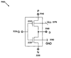
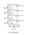
- FIG. 1 is a simplified block diagram of a logic circuit.
- the logic circuit which uses a previously proposed GDI design, is based upon two complementary transistor networks, which connect to the previously proposed GDI circuit logic inputs and outputs, and implement the desired logic function.
- the relationship between the structures of the two transistor networks and the overall function of the previously proposed GDI circuit is discussed below, for the general case and for specific transistor network configurations.
- Logic circuit 100 contains P logic block 110 , N logic block 120 , first and second logic inputs, 130 and 140 , and three logic terminals: first and second dedicated logic terminals, 150 and 160 , and common diffusion logic terminal 170 .
- the first and second dedicated logic terminals, 150 and 160 , and the common diffusion logic terminal 170 can each serve as either a logic signal input terminal or a logic signal output terminal, depending upon the specific logic circuit implementation.
- the examples given below illustrate several logic circuit terminal configurations.
- the P logic block 110 contains a network of p-type transistors 180 which are interconnected to implement a given logic function.
- the P logic block 110 has three logic connections: an outer diffusion connection 181 (at an outer diffusion node of one of the p-type transistors), a gate connection 182 (at the gate of one of the p-type transistors), and an inner diffusion connection 183 (at the second inner diffusion node of one of the p-type transistors).
- Outer diffusion connection 181 connects to the first dedicated logic terminal 150
- gate terminal 182 connects to the first logic input 130 .
- the N logic block 120 contains a network of n-type transistors 190 which implement the complementary logic function, and is structured similarly to the P logic block 110 .
- the inner diffusion nodes of the P and N logic blocks, 183 and 193 are connected together to form the common diffusion logic terminal 170 .
- the p-type and n-type transistors may be field effect transistors (FET), CMOS transistors (p-well, n-well, or twin-well), SOI transistors, SOS transistors, or the like.
- FET field effect transistors
- CMOS transistors p-well, n-well, or twin-well
- SOI transistors SOI transistors
- SOS transistors SOS transistors
- p-well and n-well CMOS transistors may be used only for a limited number of logic circuit configurations. Note that the customary distinction between the source and drain of the transistor can not be made with the previously proposed GDI structure, since for any given transistor the relative voltages between the transistor diffusion nodes changes depending upon the logic input and output voltages. This is in contrast with the standard complementary CMOS structure in which the source or drain is tied to a constant voltage.
- one of the two transistor diffusion nodes (not the gate) is arbitrarily selected to serve for the inner diffusion connection, and the other to serve for the outer diffusion connection.
- Many of the previously proposed GDI cell topologies can be implemented in standard p-well or n-well CMOS technology, due to interference of bulk effects under certain input/output conditions.
- Previously proposed GDI logic circuits are therefore preferably implemented in either twin-well CMOS or silicon-on-insulator/silicon-on-sapphire (SOI/SOS) technologies, which do not suffer from these limitations.
- the common logic terminals are connected together to form a common logic input 196 .
- a logic signal at the common logic input 196 is applied to both the P and N logic blocks, 110 and 120 .
- the logic input terminals, 130 and 140 are not connected, and each logic block has an independent logic input.
- the previously proposed GDI* circuit is discussed in greater detail below (see FIG. 8 ).
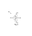
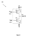
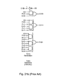
- FIG. 2 is a simplified circuit diagram of a standard previously proposed GDI logic cell.
- the p-type and n-type transistor networks each contain a single transistor, 210 and 220 respectively.
- the previously proposed GDI cell has a common input terminal (G) 230 connected to the gates of both the NMOS and PMOS transistors, a first dedicated logic terminal (P) 240 at the outer diffusion node of the PMOS transistor, and a second dedicated logic terminal (N) 250 at the outer diffusion node of the NMOS transistor 220 .
- G common input terminal
- P first dedicated logic terminal
- N second dedicated logic terminal
- the common diffusion logic terminal (D) 260 is connected to the inner diffusion nodes of both transistors.
- the first and second dedicated logic terminals, 240 and 250 , and the common diffusion logic terminal 260 may be used as either input or output ports, depending on the circuit structure.
- FIG. 2 omits bulk connections, although such connections may be required for some transistor technologies, including CMOS.
- the circuit diagrams for the previously proposed GDI logic circuits presented below have transistor bulk connections, and are therefore appropriate only for technologies with four-terminal transistors (i.e. transistors having gate, drain, source and bulk terminals), such as twin-well CMOS and SOI. Bulk connections may not be needed for some transistor technologies, such as floating bulk SOI.
- Table 1 shows six logic functions which can be implemented with a single previously proposed GDI logic cell.
- the most general case is the multiplexer (MUX), where logic signal A is applied to the common input 230 .
- Signal A selects one of the dedicated logic terminals, 240 or 250 , and the logic cell outputs the selected logic signal at the common diffusion logic terminal 260 .
- Other configurations listed in the table implement OR, AND, and inverter logic gates.
- the logic cell also implements the F1 function ( ⁇ B) and the F2 function ( ⁇ +B). Both the F1 and F2 functions are complete logic families, which can be used to realize any possible logic function.
- F1 and F2 are complete logic families.
- F1 is the only GDI function that can be used for higher level circuit design that can be realized in a standard n-well CMOS process.
- the bulks of all NMOS transistors are constantly and equally biased, since the N terminal (first dedicated logic terminal) is tied low for all logic input levels.
- the N terminal is either tied high (OR gate), or varies according to the logic input levels (F2, AND, and MUX).
- F2 can be realized in p-well CMOS.
- the previously proposed GDI cell 200 differs significantly from the standard CMOS inverter, which it resembles structurally.
- Dedicated logic inputs 240 and 250 serve as logic signal inputs, not for applying pull-up and pull-down voltages as in the CMOS case.
- a simple change of the input configuration of the previously proposed GDI cell 200 corresponds to different Boolean functions. Most of these functions are complex (6-12 transistors) in CMOS, as well as in standard PTL implementations, but require only 2 transistors as a previously proposed GDI logic circuit.
- the bulks of transistors 210 and 220 may be connected to dedicated logic terminals 240 and 250 respectively, so that the transistors 210 and 220 can be arbitrarily biased. This is in contrast with a CMOS inverter, which cannot be biased.
- the previously proposed GDI cell structure provides advantages over both CMOS and PTL logic circuits in design complexity, transistor count and power dissipation.
- An operational analysis of the previously proposed GDI logic cell is now presented, in which previously proposed GDI circuit transient behavior, swing restoration, and switching characteristics are analyzed.
- the voltage level of F1 is V Tp (instead of the expected 0V), because of the poor high-to-low transition characteristics of PMOS pass-transistors (see W. Al-Assadi, A. P. Jayasumana and Y. K. Malaiya, “Pass-transistor logic design”, International Journal of Electronics, 1991, vol. 70, no. 4, pp. 739-749, contents of which are hereby incorporated by reference).
- the previously proposed GDI cell operates as a regular CMOS inverter, which is widely used as a digital buffer for logic level restoration.
- the previously proposed GDI cell functions as an inverter buffer and recovers the voltage swing.
- the previously proposed GDI logic circuits shown below assume worst-case swing effects, and contain additional circuitry for swing restoration.
- I D ⁇ I D0 ⁇ ( W L ) ⁇ ⁇ ( q ⁇ V GS KT ) ( V GS ⁇ V TH ⁇ : ⁇ sub-threshold region ) K ⁇ ⁇ ( V GS - V TH ) ⁇ V DS - 0.5 ⁇ V DS 2 ⁇ ( V DS ⁇ V GS - V TH ⁇ : ⁇ linear ⁇ ⁇ region ) 0.5 ⁇ K ⁇ ( V GS - V TH ) 2 ( V DS ⁇ V GS - V TH ⁇ : saturation ⁇ ⁇ region ) ⁇ ( 1 )
- K is a drivability factor
- V TH is a threshold voltage
- W is a channel width
- L is a channel length.
- V GS is used as an input voltage
- V DS the voltage input variable to the Shockley model
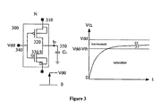
- FIG. 3 shows the previously proposed GDI circuit diagram and transient response when a step signal is supplied to the first dedicated logic terminal 310 of the previously proposed GDI cell 300 .
- the applied step signal causes a response, during which the NMOS transistor 330 passes from the saturation to the sub-threshold region, and a swing drop in output occurs.
- the transient analysis assumes a fast input transition, so that the linear region is ignored.
- Analytical expressions that describe the transient response can be derived from (1), for a capacitive load, C L 350 , at the output.
- the capacitive current is:
- C is the output capacitance
- V S is the voltage across the capacitance C L
- I C is the current charging the capacitor, which is equal to I D , the drain current through the N-channel device.
- the capacitance C includes both diffusion and well capacitances of the driven cell.
- t + k 1 1 b 2 - 4 ⁇ a ⁇ ⁇ c ⁇ ln ⁇ ( 2 ⁇ aV s + b - b 2 ⁇ 4 ⁇ a ⁇ ⁇ c 2 ⁇ aV s + b + b 2 ⁇ 4 ⁇ a ⁇ ⁇ c ) ( 7 )
- t time in saturation region
- the solution of (7) is obtained numerically (e.g. in MATLAB) for specific values of a, b, and c.
- V S After entering the sub-threshold region, V S continues rising while the output capacitance is charged by I D according to (1):
- the analysis of propagation delay of a basic previously proposed GDI cell given by equations (2-7) can be refined by taking into account the effect of the diode between the NMOS source and body. This diode is forward biased during the transient (see FIG. 2 ). By conducting an additional current, the diode contributes to charging the output capacitance C L .
- the I BS current should be added to equation (2) to derive an improved propagation delay, indicating a faster transient operation of previously proposed GDI cell.
- the swing restoration performance of previously proposed GDI circuits is calculated taking into account the area (power) and circuit frequency (delay) constraints.
- the simplest method of swing restoration is to add a buffer stage after every previously proposed GDI cell.
- the addition of a buffer stage prevents the voltage drop, but requires greater previously proposed GDI circuit area and increases circuit delay and power dissipation, making such a simplified method highly inefficient.
- Various buffering techniques are presented in the literature.
- N 1 0.3 ⁇ V DD V drop ( 14 )
- V drop As shown in FIG. 3 , after exiting the saturation area, the value of V drop is equal to V TH , and decreases with time as follows, using (9):
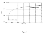
- FIG. 4 presents Cadence Spectre simulation results of the response of a previously proposed GDI AND gate to a 0-3.3 V step input, for a gate operating in the sub-threshold region with a V DD of 3.3 V.
- Interconnection effects can cause a drop in signal potential level, particularly over long interconnects. Where maintaining signal levels is essential, expression (15) may be extended to take into account the interconnection drop IR (where R is the interconnect resistance and I is the current through the interconnect).
- the resistance of the interconnect wire is given by:
- R ⁇ square ⁇ L wire W wire ( 16 ) where ⁇ square is a metal sheet resistance per square.
- I wire V DD - V drain R ( 17 )
- V drain is determined by the equalization between the wire and NMOS transistor currents as follows:
- Scaling namely V DD reduction and threshold non-scalability, influences the number of required buffers for previously proposed GDI circuit architecture according to (14).
- additional buffers may be required.
- the direct impact of adding buffers is primarily on circuit area and the number of gates.
- Buffer insertion need be considered only when linking previously proposed GDI cells through diffusion inputs. No buffers are needed before gate inputs of previously proposed GDI cells. Due to this feature, the “mixed path” topology can be used as an efficient method for buffer insertion. The number of buffers may be reduced by alternately involving diffusion and gate inputs in a given signal path. The circuit designer can trade off between buffer insertion, and delay, area and power consumption, to achieve efficient swing restoration.
- FIG. 5 shows a previously proposed GDI cascade represented as an RC tree, where R i are the effective resistances of the conducting transistors, and Ci are the capacitive loads caused by following devices.
- a resistance R ii is defined as the resistance of the path between the input and the output (for an RC tree without side branches).
- R kk is the resistance between the input and node k.
- C k is the capacitance at node k.
- T D ⁇ k ⁇ ⁇ R kk ⁇ C ( 22 )
- T R ( ⁇ k ⁇ ⁇ R kk 2 ⁇ C k ) / R ii ( 23 )
- the maximal delay of the RC tree can be derived numerically from the bounds on the time of equations (22) and (23), and is given by the following equation: t ⁇ T D ⁇ T R ⁇ T D ln[1 ⁇ i ( t )] (24)
- the number of stages between buffers should be limited to satisfy both the successive swing restoration and the maximal delay requirements.
- the maximal number of stages in cascade between two buffers is therefore the minimal value between N1 (given by (14)) and N2.
- FIG. 6 shows the structure of a previously proposed GDI (or prior-art CMOS) inverter 600 , along with its equivalent digital model 610 .
- the digital model of the previously proposed GDI inverter consists of three parallel branches between V DD and ground. Two of the branches each consist of two capacitors in series (C inn and C inp for the first branch, and C outn and C outp for the second branch), with an inverter input between C inn and C inp .
- the third branch consists of two resistors (R n and R p ) in series, with the inverter output between the two resistors.
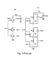
- FIG. 7 shows a circuit diagram of a CMOS NAND gate 700 , along with its equivalent digital model 710 .
- the NAND gate consists of identical n-channel metal-oxide-semiconductor FETs (MOSFETs), 720 . 1 to 720 . n , connected in series.
- MOSFETs metal-oxide-semiconductor FETs
- this ratio improves if the effect of the body-source diode in previously proposed GDI cell is considered (14), and if the delay formula in (7) is refined by including a bulk-source conduction current in (13).
- GDI cell For the analysis of fan-out bounds, the dual-transistor previously proposed GDI cell is compared to CMOS gates with equivalent functional complexity. This approach allows definition of fan-out bounds using the logic-effort concept of I. Sutherland, B. Sproull and D. Harris, “Logical Effort—Designing Fast CMOS Circuits”, Morgan Kaufmann Publishers, p. 7, contents of which are hereby incorporated by reference.
- the above fan-out improvement values are correct for the gate input of a previously proposed GDI cell, for which the previously proposed GDI cell characteristics are similar to those of the CMOS inverter. If the diffusion input is considered, an additional factor is applied to represent the capacitance ratio between the gate and diffusion inputs, and the factors given above are multiplied by C Gate /C Diff . Both capacitance parameters are defined by the design technology.
- the GDI logic cell shows improvement over comparable CMOS logic in terms of delay, number of transistors, area, and power consumption.
- GDI logic circuits have certain drawbacks, which are primarily related to input connections to MOSFET wells. Firstly, GDI logic circuits may experience a threshold drop, and, in some cases, an increased diffusion input capacitance. Both effects exist in PTL techniques as well, and were considered in the simulations and analysis presented herein. Secondly, there is a relative increase of circuit area due to separated MOSFET wells (comparisons based on actual logic gate layouts are presented below).
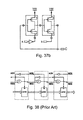
- the previously proposed GDI cell shown in FIG. 2 has a connection between the two common logic terminals connection.
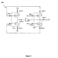
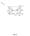
- FIG. 8 is a circuit diagram of a logic circuit having separate common logic terminals.
- the logic cell of FIG. 8 is designated herein as a double-gate-input previously proposed GDI cell (prior-art GDI*).
- the previously proposed GDI* logic cell 800 has two transistor networks, p-type networks 810 and n-type transistor network 820 , which each contain a single transistor.
- the previously proposed GDI* cell has two logic input terminals, I ( 830 . 1 ) and I* ( 830 .
- the common diffusion logic terminal (D) 850 is connected to the drains of both transistors.
- I and I′ are provided with mutually exclusive signals. Ensuring that the input signals are mutually exclusive can be achieved by an appropriate circuit environment, as in a previously proposed GDI-latch, or by applying an inverter to one of the inputs.
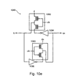
- FIG. 9 shows the structure of a latch based upon the previously proposed GDI* cell of FIG. 8 .
- the latch consists of two previously proposed GDI* cells, 910 and 920 , and inverter 930 , with logic inputs at logic terminals 920 . 1 and 920 . 2 respectively.
- the logic output is at the common diffusion terminal 920 . 5 of previously proposed GDI* cell 920 .
- the two cells are connected by inverter 930 , through which the common diffusion outputs, 910 . 5 and 920 . 5 , of the two cells are connected.
- previously proposed GDI* cell 920 are respectively connected to logic inputs 910 . 1 and 910 . 2 of the previously proposed GDI* cell 910 .
- Dedicated logic terminals, 910 . 3 and 910 . 4 , of previously proposed GDI* cell 910 are tied to V DD and ground respectively.
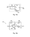
- FIGS. 10 a - 10 e are simplified diagrams of previously proposed GDI latches.
- FIG. 10 a shows a T-latch based upon the previously proposed GDI* latch of FIG. 9 .
- T-Latch 1000 consists of a previously proposed GDI flip-flop 1012 and inverter 1014 .
- the logic signal is input at terminal T 1013 , and is fed through inverter 1014 to input A 1015 of TFF 1000 , and directly to input B 1016 of flip-flop 1012 .
- the inputs of the T-Latch are connected through inverter 1014 , so that an efficient 8-transistors implementation is achieved.
- FIG. 10 b shows a T-latch 1020 based on the standard previously proposed GDI cell.
- FIG. 10 b is a circuit diagram of a previously proposed GDI T-latch.
- T-latch 1020 consists of previously proposed GDI cell 1030 , and three inverters 1041 to 1043 .
- the logic signal is input to the common logic input (G) of previously proposed GDI cell 1030 .
- the output at the common diffusion terminal (D) of previously proposed GDI cell 1030 is connected to the T-Latch output Q via inverter 1043 .
- Inverters 1041 and 1042 feed back the output signal to the dedicated logic terminals (P and N) of previously proposed GDI cell 1030 . Note that in FIG.
- inverters INV 2 1042 and INV 3 1043 are added for swing restoration and can be eliminated in zero-V TH technologies. In any case the implementation is effective, and more compact than CMOS alternatives.
- the presented circuit can be extended to TFF by adding an edge detector circuit containing two previously proposed GDI cells (NOT and AND).
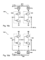
- FIGS. 10 c , 10 d , and 10 e Three previously proposed GDI D latches are shown FIGS. 10 c , 10 d , and 10 e .
- FIG. 10 c shows the structure of a previously proposed GDI F1-based D-latch 1050 .
- D-latch 1050 consists of two previously proposed GDI cells, 1060 and 1062 , AND gates, 1070 and 1072 , and inverter 1074 .
- the common diffusion terminal of previously proposed GDI cell 1060 is connected to the common logic input of previously proposed GDI cell 1062 .
- the D and CLK latch inputs are connected via AND gates 1070 and 1072 , and inverter 1074 to the first dedicated logic terminals of the previously proposed GDI cells, 1060 and 1062 .
- the second dedicated logic terminals of the previously proposed GDI cells, 1060 and 1062 are tied to ground.
- FIG. 10 d shows the structure of a previously proposed GDI F2-based D-latch 1070 .
- D-latch 1070 is structured similarly to D-latch 1050 of FIG. 10 c , but has the AND gate outputs connected to the second dedicated logic terminals of the two previously proposed GDI cells, and the first dedicated logic terminals tied high.
- D-latch 1090 consists of two previously proposed GDI cells, 1092 and 1093 , and inverters, 1094 and 1095 .
- Inverter 1094 is connected between the common diffusion output of previously proposed GDI cell 1093 and the second dedicated logic terminal of previously proposed GDI cell 1092 .
- Inverter 1095 is connected between the common diffusion terminal of previously proposed GDI cell 1092 and the second dedicated logic terminal of previously proposed GDI cell 1093 .
- the D-latch inputs and outputs are at the first dedicated logic terminals of the two previously proposed GDI cells, 1092 and 1093 , and the inverter inputs.
- D-latch 1050 and D-latch 1080 latch on the falling edge of the clock
- D-latch 1090 latches on the rising edge of the clock.
- the edge used to latch the data is selected by the circuit designer by providing the proper logic at the clock input.
- FIGS. 2-10 are based on a dual-transistor previously proposed GDI (or previously proposed GDI*) logic cell, which has a single transistor in each of the two logic blocks.
- the multi-transistor previously proposed GDI logic circuit each logic block contains a transistor network composed of multiple transistors.
- the logic blocks may have more than one common logic input, where each additional common logic terminal is connected to the gates of complementary transistors in both of the transistor networks.
- Table 1 lists the various logic functions which can be provided by a single previously proposed GDI cell.
- the previously proposed GDI cell is an extension of a single-input CMOS inverter structure a triple-input logic structure.
- the two additional inputs of the previously proposed GDI cell are provided by the first and second dedicated logic terminals, which in the CMOS cell do not serve as logic terminals but instead are tied to a fixed voltage.
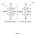
- FIG. 11 is a simplified block diagram of a comparison between an n-input CMOS logic gate and an (n+2)-input previously proposed GDI logic circuit.
- Previously proposed GDI circuit 1100 consists of two n-input logic blocks, 1110 and 1120 , with additional logic inputs at the P and N terminals, yielding a total of n+2 logic inputs.
- CMOS circuit 1140 is similarly composed of two n-input logic blocks, 1150 and 1160 , however the P and N terminals are tied to V DD and V SS respectively, and do not serve as logic terminals.
- Extension of any n-input CMOS structure to an (n+2)-input previously proposed GDI cell can be done by introducing a logic input at the first dedicated logic terminal (P) of the PMOS block 1110 (instead of the supply voltage V DD ), and a second logic input at the second dedicated logic terminal (N) in the NMOS block 1120 (instead of V SS ).
- a previously proposed GDI circuit having more than one transistor in the P and N logic blocks, 1120 and 1130 is designated herein as a multi-transistor GDI circuit. (A comparable extension can be made to any complementary transistor structure, and is not limited to CMOS.)
- FIG. 12 shows a previously proposed GDI circuit 1200 , having logic blocks 1210 and 1220 , consisting of triple-input transistor networks (inputs A, B, and C). The two logic blocks implementing complementary logic functions. Since the P and N terminals previously proposed GDI logic circuit 1200 serve as logic inputs, there are five logic terminals in all. A complementary CMOS logic circuit having the same structure would have only three logic inputs (A, B, and C).
- Equation (32) can be used to implement a Shannon expansion (see E. Shannon, W. Weaver, “The Mathematical Theory of Information”, University of Illinois Press, Urbana—Champaign, Ill., 1969, contents of which are hereby incorporated by reference).
- x 1 0 (34)
- Extended previously proposed GDI circuit 1300 consists of an n-input switching block 1330 (which may be either a previously proposed GDI cell or a multi-transistor previously proposed GDI circuit). Further logic inputs are provided to logic gates 1310 and 1320 . The logic output of logic gate 1310 is connected to the first dedicated input of switching block 1330 , and the logic output of logic gate 1320 is connected to the second dedicated input of switching block 1330 . Extended previously proposed GDI circuit 1300 operates essentially as a multiplexer, selecting between logic gate A 1310 and logic gate B 1310 .
- Logic gates 1310 and 1320 implement functions A(Xn+1 . . . Xp) and B(Xp+1 . . . Xr) respectively, in any technologically compatible manner.
- Switching block 1330 connects between the logic gates and the following logic block C 1340 .
- F(x1 . . . xn) only one of the functions will drive the data computed as a result of its input transitions, while the data transitions from the other function are prevented from propagating to the next logic block C.
- the previously proposed GDI logic circuits (i.e. previously proposed GDI cell, previously proposed GDI* cell, multi-transistor previously proposed GDI circuit, and extended previously proposed GDI circuit) described above can serve as building blocks for more complex logic circuits.
- the applicability of the Shannon expansion (33 and 34) to any logic function allows a previously proposed GDI implementation of any digital circuit, thereby achieving a low power implementation of the logic function. Due to their special properties, previously proposed GDI logic circuits can be used for design of low-power combinatorial circuits.
- Two or more previously proposed GDI logic circuits are interconnected to form a higher order previously proposed GDI logic circuit.
- Several higher order logic circuits composed of interconnected previously proposed GDI logic cells are given below, along with performance data.
- FIG. 14 is a simplified flowchart of a recursive algorithm for implementing logic functions by previously proposed GDI cells.
- the algorithm synthesizes any combinatorial function by means of 3-input previously proposed GDI cells.
- the algorithm's steps may be summarized as follows:
- G stands for previously proposed GDI and ‘NG’ for an inverted previously proposed GDI cell that is inserted post-process in order to maintain signal integrity.
- This approach can be used in combination with existing cell library-based synthesis tools to achieve an optimized design.
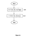
- FIG. 15 is a simplified flowchart of a method for designing a logic circuit.
- FIG. 15 presents the method of FIG. 14 in more detail, but essentially involves the same recursion, to progressively simplify the logic function.
- Each recursion reduces the number of function variables by one, until eventually the required function can be represented as an interconnected network of simple previously proposed GDI multiplexing cells. Once a single variable representation has been reached, the recursion cycles end, combining the previously proposed GDI cells into a structure that performs the specified logic function.
- the method thus provides a logic circuit design consisting of interconnected previously proposed GDI logic cells.
- the logic cells are dual-transistor previously proposed GDI cells, as shown in FIG. 2 .
- step 1500 a logic function having at least one logic variable is received.
- the logic function to be synthesized, F is set equal to the received logic function in step 1510 .
- the synthesis recursion cycle begins at step 1515 .
- step 1520 the synthesized function is checked to determine if it is a non-inverted single logic variable X. If so, a connection for a logic input is provided in step 1525 . The synthesis recursion cycle is then discontinued.
- step 1530 the synthesized function is checked to determine if it is a high logic level. If so, a logic design consisting of a connection to a high logic level is provided in step 1535 . The synthesis recursion cycle is then discontinued.
- step 1540 the synthesized function is checked to determine if it is a low logic level. If so, a logic design consisting of a connection to a low logic level is provided in step 1545 . The synthesis recursion cycle is then discontinued.
- a Shannon expansion of F is performed to reduce the number of logic variables by one.
- a first logic function H a second logic function J are extracted from a Shannon expansion of the synthesized function for a selected logic variable Xn.
- a recursion cycle is then performed for each of the extracted functions, to obtain a circuit design for functions H and J.
- the recursion cycle for function H involves setting the synthesized function to H in step 1560 , and entering a new recursion cycle at step 1515 .
- a sub-circuit design of interconnected previously proposed GDI cells is provided for function H.
- step 1570 the synthesized function is set to Z, and a new recursion cycle is entered at step 1515 .
- a sub-circuit design of interconnected previously proposed GDI cells is provided for function J.
- step 1580 the sub-circuit designs obtained for functions H and J are combined using a previously proposed GDI cell.
- a final logic circuit design is provided consisting of a logic element with the selected logic variable at the common logic terminal G, the output of the first sub-circuit connected to the first dedicated logic terminal P, and the output of the second sub-circuit connected to a second dedicated logic terminal N.
- the logic circuit output is at the logic element common diffusion terminal.
- step 1550 The Shannon expansion of the logic function being synthesized is performed in step 1550 .
- FIG. 16 is a simplified flowchart of a method for extracting the first and second logic functions (H and J) from the synthesized function.
- Xn 1 ⁇ .
- Xn 0 ⁇ .
- the previously proposed circuit design method includes the further step of inserting buffers into the logic circuit design.
- Equations (14) and (25) are used to calculate the values of N1 and N2, and the maximal number of stages which can be cascaded between two buffers equals the minimal value between N1 and N2.
- the resulting value indicates that a buffer is required after every two cascaded previously proposed GDI cells.
- Buffer elements are inserted between previously proposed GDI cells to prevent the occurrence of chains that exceed a specified length.
- the buffer elements may consist of one or more inverters.
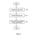
- FIG. 17 is a simplified flowchart of a method for providing a previously proposed GDI logic circuit.
- a previously proposed GDI logic circuit is designed for a specified function by the method of FIG. 15 .
- the required previously proposed GDI cells are provided, and in step 1720 the previously proposed GDI cells are connected as specified by the circuit design.
- One advantage of the abovedescribed methods is the ability to calculate the maximal number of transistors needed for implementation of an n-input function, before the actual logic circuit design.
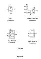
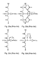
- FIGS. 18 a , 18 b , and 18 c show previously proposed GDI XOR, AND, and OR gates respectively, and their equivalents in CMOS, TG, and NMOS Pass-Gate (N-PG) technologies.
- the cells were designed for a minimal number of transistors for each technique.
- a buffer was added to the N-PG cells, because of low swing of output voltage (V drop >0.3 V DD ).
- Most circuits were implemented with a W/L ratio of 3, to achieve the best power-delay performance.
- the circuits were simulated using Cadence Spectre at 3.3V, 40 Mhz and 27° C., with a load capacitance of 100 fF. In the simulations the well capacitance and other parasitic parameters were taken into account.
- Each set of comparisons includes a logic cell implemented in the four logic techniques: previously proposed GDI, CMOS, Transmission Gate and n-MOS Pass Gate. The same logic value transitions were supplied to the inputs of the test circuits for each technique. Measured values apply to the transitions of inputs connected to the transistor gates, in order to achieve a consistent comparison.
- the measured power is that of the DUT, including the power consumed by driving the next stage, thus accounting for the input power consumption, and not just the power directly consumed from supply.
- This configuration gives more realistic environment conditions for test circuit, instead of the ideal input transitions of simulator's voltage sources.
- Results are given for power dissipation in different gates.
- the MUX gate has the largest power consumption of all the logic gates, because of its complicated implementation (particularly in CMOS) and the presence of an additional input.
- the AND gate's power dissipation is the minimal amongst all the gates.
- Most of previously proposed GDI logic gates prove to be the most power efficient in comparison with the four other design techniques (only for the F2 gate is there an advantage of N-PG over the previously proposed GDI gate).
- previously proposed GDI proves to have the best performance values and the lowest transistor count. Even in the cases where the power or delay parameters of some previously proposed GDI gates are inferior, relative to TG or N-PG, the power-delay products and transistor count of previously proposed GDI are lower. Only the TG design method is a viable alternative to previously proposed GDI if a high frequency operation is of concern.
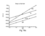
- FIG. 19 shows power and delay results for OR and AND cells under different load conditions, for the previously proposed GDI (F1 configuration), CMOS and PTL techniques.
- the simulations were carried out in SPECTRE to compare previously proposed GDI NOR and AND cells implemented in CMOS, N-PG, and TG, in 0.24 ⁇ m CMOS technology.
- a regular CMOS inverter was used as a load for the DUT, with dimensions of 2.4 ⁇ m/0.24 ⁇ m for PFET and 0.9 ⁇ m/0.24 ⁇ m for NFET.
- load size applies a load capacitance of about 1 fF.
- load size was multiplied by a scaling parameter, PS, varying from 1 to 3.
- PS scaling parameter
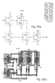
- FIG. 20 shows GDI circuits and layouts for basic functions for a regular p-well process.
- CLA Carry-Lookahead Adder
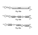
- FIG. 21 shows examples of generic carry-lookahead adders.
- FIG. 21 a is a basic scheme
- FIG. 21 b is a 3-bit carry generator.
- the PG generation and SUM generation circuits surround a carry-generate block.
- the circuit presented is 4-bit adder that can be replicated in order to create 8-bit adder, due to fan-in and size limitations of the gates.
- FIG. 22 shows a four-bit ripple comparator consisting of a cascade of 4 identical basic units, while the comparison data is transmitted through the units. Comparison of the MSB digit is done first, proceeding down to the LSB. The outcome of comparison in every unit is represented by two signals C and D according to Table 6.
- Every basic unit includes two inputs of comparison data from previous units.
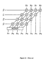
- FIG. 23 shows the structure of a 4-bit multiplier.
- the multiplier contains an array of interconnected basic cells.
- the multiplier circuit is based on the generation of partial products and their addition, thereby creating a final product.
- the following equations represent both the multiplied numbers and the product:
- Each multiplier cell represents one bit of partial product and is responsible for:
- the cell consists of two components—an AND gate to generate the partial product bit, and an adder to add this bit to the previous sum.
- Simulation results were used to make performance comparisons of some of the higher order digital circuits mentioned above. All given measurements were carried out on a representative pattern of possible input transitions, with the worst case assumption used to find a maximal delay of the circuit, and the power dissipation was calculated as an average over the pattern.
- Results are now presented for an eight-bit CLA adder.
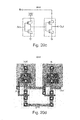
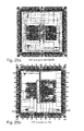
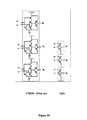
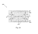
- An eight-bit adder was realized in a 1.6 ⁇ m CMOS process. Two chips were designed, and their layouts are shown in FIG. 25 .
- FIG. 25 a shows a CLA in previously proposed GDI and CMOS
- FIG. 25 b shows a CLA in previously proposed GDI and TG.
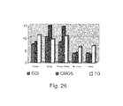
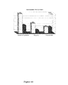
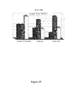
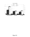
- Several parameters were measured: average power, maximal delay, power-delay product, number of transistors and circuit area. The results are assembled in Table 7 and FIG. 26 .
- the previously proposed GDI Adder proves to be the most power efficient circuit. Power dissipation in previously proposed GDI is less than in CMOS and in TG, yet the delay of TG is less than that of previously proposed GDI.
- the CMOS circuit has the highest delay, 44.9% more than previously proposed GDI.
- the power-delay product of previously proposed GDI is less than both TG and CMOS. Because of the use of limited previously proposed GDI cell library in p-well CMOS process, the number of transistors and area of CMOS and previously proposed GDI circuits are close, but much less than in the TG Adder implementation.
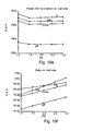
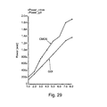
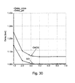
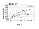
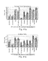
- FIGS. 29-31 show the changing of power ( FIG. 29 ), delay ( FIG. 30 ), and power-delay product ( FIG.
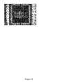
- An 8-bit Adder designed in previously proposed GDI and CMOS was fabricated in 1.6 ⁇ m CMOS technology (MOSIS). The voltage supplies of the two circuits were separated in order to enable a separate power measurement. After the post-processing, three types of ICs were available: previously proposed GDI Adder, CMOS Adder, and ICs containing both circuits connected. Measurements of the dynamic power of the circuits could thus be carried out, while eliminating the static power dissipation and power dissipation of output pads, which contain buffers and additional circuitry. A photograph of the test chip is shown in FIG. 32 .
- Dynamic power measurements were performed for various frequencies, respectively to the voltage supply level. For a 5V supply, the measurements were performed at 12.5 MHz; for a 4.5V supply at 10 MHz; and for other supply voltages at 4 MHz.
- the normalized power-delay product Due to the equal delay values in both circuits (see Table 10), the normalized power-delay product has about the same values as those of power measurements. For power and power-delay product, improvements in the range of 11% to 45% were measured.
- Previously proposed GDI implementations were also analyzed for the class of asynchronous circuits. The results presented above show that combinational previously proposed GDI circuits are fast and low power relative to CMOS and PTL implementations. C-elements and SR latches are compared with a variety of CMOS state holding circuits. A bundled-data controller and two qDI combinational logic circuits (a XOR gate and a full adder) demonstrate that systems employing previously proposed GDI components outperform standard CMOS implementations in area, power, and speed. Furthermore, previously proposed GDI components provide some enhanced hazard tolerance. All designs were validated and compared using SpectreS simulations.
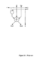
- C-elements are frequently used in asynchronous design.
- the C-element changes its output only when both inputs are identical.
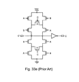
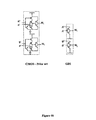
- the previously proposed GDI C-element was compared to the five CMOS C-element circuits shown in FIG. 33 : dynamic ( FIG. 33 a ), conventional ( FIG. 33 b ), weak feedback ( FIG. 33 c ), static ( FIG. 33 d ), and symmetric ( FIG. 33 e ) circuits.
- the symmetric circuit ( FIG. 33 d ) has been identified by Al-Assadi et al. as the most energy-efficient and high-speed implementation from amongst the dynamic, conventional, weak feedback, and symmetric circuits.
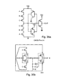
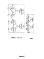
- FIG. 34 shows three previously proposed GDI implementations of the C-element.
- the truth table for the C-element is given in Table 12.
- the dynamic previously proposed GDI C-element ( FIG. 34 a ) comprises two previously proposed GDI cells with cross-connected diffusion areas.
- the common diffusion terminal of the previously proposed GDI cell is used both as input (B) and output (C).
- the outer diffusion connections of each previously proposed GDI cell are used as bi-directional terminals.
- the dynamic previously proposed GDI C-element employs only four transistors, as compared to six transistors in the CMOS dynamic circuit ( FIG. 33 a ).
- the static previously proposed GDI C-element ( FIG. 34 b ) employs eight transistors, including four in a keeper, as compared with 10 in the static CMOS circuit ( FIG. 33 d ).
- the conducting path from input B to the output is connected and the signal B propagates to the output.
- a ⁇ B the B-to-C path is disconnected and the output is left unchanged.
- CMOS C-elements contain pull-up paths that traverse two PMOS transistors in series. This difference contributes to the lower delay of the dynamic previously proposed GDI C-element.
- the B input does not drive any gates of the previously proposed GDI cells; rather, it is only gated to the output through pass transistors.
- the signal path to the output is double-controlled, by the other input (A) and by the output (C). This double-control reduces the probability of output hazards.
- This advantage is extremely useful in asynchronous design, where the C-element is often assumed an atomic, hazard free building block (see J. Spars ⁇ and S. Furber (eds.), Principles of asynchronous circuit design—A systems perspective, Kluwer Academic Publishers, 2001).
- the B signal degrades by at least one V T .
- the signal needs to drive not only the load, but also the feedback inverter. Consequently, the B ⁇ C path becomes critical in the C-element.
- the B signal presents an increased load on the previous stage (which sources B).
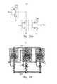
- FIGS. 35 a and 35 b Previously proposed GDI and CMOS three-input C-elements are shown in FIGS. 35 a and 35 b respectively.
- the three-input C-element is useful in qDI combinational logic, as will be discussed below.
- the problem of a high PMOS stack in CMOS C-elements is somewhat mitigated in the previously proposed GDI circuit.
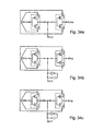
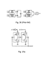
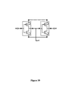
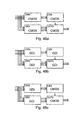
- a C-element can be replaced by an SR latch when the inputs are mutually exclusive, as shown in FIG. 36 .
- Previously proposed GDI implementations of the C-element by SR latch are presented in FIGS. 37 a and 37 b (F1 and F2 based respectively).
- FIG. 36 the A input is inverted, as is typically useful in asynchronous circuits.
- the implementation is area-efficient: The SR latch requires only two previously proposed GDI cells (four transistors).
- the mutual exclusivity of the SR inputs contributes to the fact that no V T drop is observed in the circuit.
- the drop can occur only when 0 is applied to the diffusion input of one of the previously proposed GDI cells in the F1-SR latch, or when 1 is applied to one of the previously proposed GDI cells in the F2 circuit.
- the second previously proposed GDI is biased as a simple inverter, and restores the voltage swing.
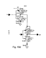
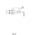
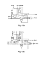
- FIG. 40 illustrates the simulation environment.
- the C-element is driven by two inverters, which are driven by ideal sources, to imitate the real environment and signals.
- the inverters are also useful for measuring the current flow from V DD that is caused by transitions in the diffusion inputs in previously proposed GDI which sink current from the previous logic stage.
- the C-element drives a 100 fF load capacitor.
- Other transistors are 1 ⁇ m/1 ⁇ m for NMOS and 4 ⁇ m/1 ⁇ m for PMOS.
- the weak inverter size is 1 ⁇ m/4 ⁇ m. Simulation results are presented below.
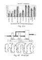
- the dynamic previously proposed GDI C-element is the fastest circuit, showing up to 89% maximal delay decrease compared to standard CMOS techniques, and a 63% improvement compared to the symmetric C-element, which is the fastest technique among CMOS circuits.
- Dynamic and SR-based previously proposed GDI circuits are the most area efficient (requiring up to 33% fewer transistors than CMOS).
- Buffered previously proposed GDI requires the highest number of transistors amongst the previously proposed GDI circuits (12 transistors).
- CMOS C-elements are preferred over previously proposed GDI for some static circuits, but in other cases the dynamic previously proposed GDI C-element or the previously proposed GDI SR latch may offer a superior solution.
- SR-F1, SR-F2 and the dynamic previously proposed GDI demonstrate the shortest delay among all circuits.
- the delay improvement in previously proposed GDI is in the 22%-82% range compared to CMOS.
- the inverted input previously proposed GDI C-element is slower than the non-inverted input one. This is due to the fact that while in the non-inverted previously proposed GDI each path through the pass-transistors contains one NMOS and one PMOS transistors, in the inverted input previously proposed GDI one of the paths goes through two PMOS transistors.
- inverted-input CMOS circuits are bigger than non-inverted ones, and the opposite is true for the SR-based previously proposed GDI circuits.
- Other previously proposed GDI circuits have the same size in both cases.
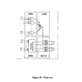
- FIG. 42 shows the filter structure and the STG flow for a Bundled-Data Filter Controller (see J. Cortadella, M. Kishinevsky, A. Kondratyev and L. Lavagno, “Introduction to asynchronous circuit design: specification and synthesis,” Tutorial, Async. Conference, 2000, contents of which are hereby incorporated by reference).
- the Petrify CMOS implementation of the controller is shown in FIG. 43 a .
- a CMOS Symmetric C-element is used in this comparison to obtain a low-power circuit.
- FIG. 43 a shows a CMOS-based Bundled-Data Controller.
- the inverted-input AND gates is replaced by previously proposed GDI OR gates and inverters.
- the previously proposed GDI OR element resulted in a reduced number of transistors, and the inverters help with swing-restoration.
- the inputs of the C-element are mutually exclusive, and hence it has been replaced by the smaller, faster, and lower power previously proposed GDI SR latch.
- the previously proposed GDI implementation requires only 20 transistors, as opposed to 50 in CMOS.
- the previously proposed GDI controller is approximately three times faster than the CMOS circuit, consuming about the same power.
- the reduced circuit complexity and the superior properties of the abovedescribed previously proposed GDI SR-F2 are the main contributors to the advantages of the previously proposed GDI controller.
- n-input, m-output DR-ST circuit comprises four interconnected subnets (see FIG. 45 ): ORN and CEN detect when all the inputs become defined or undefined.
- DRN is a monotonic implementation of the dual rail combinational functions, and OUTN enforces the strong conditions (all outputs remain undefined until all inputs become defined, and all outputs remain defined as long as not all inputs have become undefined).
- Other qDI techniques include Delay Insensitive Minterm Synthesis (DIMS) (see R. O. Ozdag and P. A. Beerel, “High-speed QDI asynchronous pipelines,” in Proc. International Symposium on Advanced Research in Asynchronous Circuits and Systems, pp. 13-22, April 2002, contents of which are hereby incorporated by reference) and RSPCFB (see J. Spars ⁇ and J. Straunstrup, “Delay insensitive multi-ring structures,” Integration, the VLSI journal, 15(3), 313-340, October 1993, contents of which are hereby incorporated by reference).
- DIMS Delay Insensitive Minterm Synthesis
- RSPCFB see J. Spars ⁇ and J. Straunstrup, “Delay insensitive multi-ring structures,” Integration, the
- a simple XOR gate is used as an example.
- the CMOS and previously proposed GDI implementations of the ORN and DRN subnets of the XOR DR-ST gate are presented in FIG. 46 and FIG. 47 respectively.
- Symmetric C-elements are used for the CMOS CEN and OUTN subnets, while the previously proposed GDI implementation is based on the buffered previously proposed GDI C-element.
- FIG. 48 a shows a CMOS implementation, with all four subnets as CMOS circuits.
- FIG. 48 b shows a previously proposed GDI implementation, with all four subnets as previously proposed GDI cells.
- FIG. 48 c shows a hybrid implementation, with the ORN and DRN subnets as previously proposed GDI cells, and the CEN and OUTN subnets as CMOS circuits.
- the previously proposed GDI and hybrid circuits are 38% smaller than the CMOS one.
- the previously proposed GDI circuit is slower and consumes more power than the CMOS circuit, due to the use of buffered previously proposed GDI C-elements, which are required in this case for their drive capability.
- the hybrid circuit consumes only half the power as CMOS while being just as fast. When hazard immunity and low supply voltage tolerance are critical, such as in low noise, low power applications, an all-previously proposed GDI circuit should be considered.
- CMOS and Hybrid circuits of a full adder are designed and compared.
- the ORN and DRN subnets are presented in FIG. 50 and FIG. 51 respectively, and are either previously proposed GDI or CMOS based. (In the DRN subnet Full Adder each gate may be implemented with either CMOS or previously proposed GDI.)
- the CEN subnet is based on a 3-input static CMOS C-element, while OUTN comprises 2-input symmetric CMOS C-elements.
- Decoder 5300 contains only two previously proposed GDI cells, 5310 and 5320 .
- the two previously proposed GDI cells have their logic inputs ( 5312 and 5322 ) connected together to form the decoder logic input, their first dedicated logic terminals ( 5314 and 5324 ) tied together to form Out 1 , and their second dedicated logic terminals ( 5316 and 5326 ) tied together to form Out 2 .
- Decoder 5300 is a four-transistor structure that can be used as an efficient basis for implementation of low-power area-efficient decoders. Table 13 gives the decoder truth table.
- the previously proposed GDI technology is not generally applicable to standard CMOS transistors.
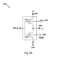
- the basic previously proposed GDI cell shown in FIG. 2 omits bulk connections, and is therefore useful as shown only for floating-bulk transistor technologies.
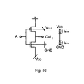
- the bulk node of PMOS transistor is connected to the node P and the bulk of NMOS transistor is connected to the node N, as shown in FIG. 54 .
- Such circuits require four-terminal transistors, and are therefore not implementable in standard n-well (or p-well) CMOS technology.
- Only certain special cases of GDI circuits, such as F1 and F2 (see Table 1), can be implemented with standard CMOS technologies (n-well CMOS and p-well CMOS technology respectively).
- a complementary logic cell contains a first logic input, a second logic input, a first dedicated logic terminal, a second dedicated logic terminal, a high-voltage terminal configured for connection to a high constant voltage a low-voltage terminal configured for connection to a low constant voltage, a p-type transistor, and an n-type transistor.
- the p-type transistor has an outer diffusion connection, a gate connection, an inner diffusion connection, and a bulk connection.
- the n-type transistor has an outer diffusion connection, a gate connection, an inner diffusion connection, and a bulk connection.
- the first dedicated logic terminal is connected to the outer diffusion connection of the p-type transistor
- the second dedicated logic terminal is connected to the outer diffusion connection of the n-type transistor
- the inner diffusion connection of the p-type transistor and the inner diffusion connection of the n-type transistor is connected to form a common diffusion logic terminal
- the high-voltage terminal is connected to the bulk connection of the p-type transistor
- the low-voltage terminal is connected to the bulk connection of the n-type transistor.
- a complementary logic circuit containing a first logic input, a second logic input, a first dedicated logic terminal, a second dedicated logic terminal, a high-voltage terminal configured for connection to a high constant voltage, a low-voltage terminal configured for connection to a low constant voltage, a first logic block, and a second logic block.
- the first logic block consists of a network of p-type transistors for implementing a predetermined logic function.
- the p-type transistor network has an outer diffusion connection, a first network gate connection, an inner diffusion connection, and a bulk connection.
- the outer diffusion connection of the p-type transistor network is connected to the first dedicated logic terminal, and the first network gate connection of the p-type transistor network is connected to the first logic input.
- the second logic block consists of a network of n-type transistors which implements a logic function complementary to the logic function implemented by the first logic block.
- the n-type transistor network has an outer diffusion connection, a first network gate connection, an inner diffusion connection, and a bulk connection.
- the outer diffusion connection of the n-type transistor network is connected to the second dedicated logic terminal, and the first network gate connection of the n-type transistor network is connected to the second logic input.
- the bulk connection of the p-type transistor network is connected to the high-voltage terminal, and the bulk connection of the n-type transistor network is connected to the low-voltage terminal.
- the inner diffusion connections of the p-type network and of the n-type network are connected together to form a common diffusion logic terminal.
- the first and second logic inputs are connected to form a first common logic input.
- each of the logic terminals is separately configurable to serve as a logic input.
- each of the logic terminals is separately configurable to serve as a logic output.
- the logic circuit further contains a third logic input connected to a second network gate connection of the p-type transistor network.
- the logic circuit further contains a fourth logic input connected to a second network gate connection of the n-type transistor network.
- the third and fourth logic inputs are connected to form a second common logic input.
- the p-type transistor network comprises a single p-type transistor.
- the n-type transistor network comprises a single n-type transistor.
- the network of p-type transistors comprises one of a group of networks comprising: a network of p-type field effect transistors (FET), a network of p-type p-well complementary metal-oxide semiconductor (CMOS) transistors, a network of p-type n-well complementary metal-oxide semiconductor (CMOS) transistors, a network of p-type twin-well complementary metal-oxide semiconductor (CMOS) transistors, a network of p-type silicon on insulator (SOI) transistors, and a network of p-type silicon on sapphire (SOS) transistors.
- FET field effect transistors
- CMOS complementary metal-oxide semiconductor
- CMOS complementary metal-oxide semiconductor
- CMOS complementary metal-oxide semiconductor
- CMOS twin-well complementary metal-oxide semiconductor
- SOI silicon on insulator
- SOS silicon on sapphire
- the network of n-type transistors comprises one of a group of networks comprising: a network of n-type FETs, a network of n-type p-well CMOS transistors, a network of n-type n-well CMOS transistors, a network of n-type twin-well CMOS transistors, a network of n-type SOI transistors, and a network of n-type SOS transistors.
- the logic circuit comprises one of a group of the following logic circuits: an OR gate, an inverted OR (NOR) gate, an AND gate, a multiplexer gate, an inverter gate, and an exclusive OR (XOR) gate.
- the logic circuit is operable to implement a ((NOT A) OR B) logic operation upon logic inputs A and B.
- the logic circuit is operable to implement a ((NOT A) AND B) logic operation upon logic inputs A and B.
- a logic circuit consisting of interconnected logic elements.
- Each of the logic elements contains a first logic input, a second logic input, a first dedicated logic terminal, a second dedicated logic terminal, a high-voltage terminal configured for connection to a high constant voltage, a low-voltage terminal configured for connection to a low constant voltage, a p-type transistor having an outer diffusion connection, a gate connection, an inner diffusion connection, and a bulk connection, and an n-type transistor having an outer diffusion connection, a gate connection, an inner diffusion connection, and a bulk connection.
- the outer diffusion connection of the p-type transistor is connected to the first dedicated logic terminal, and the gate connection of the p-type transistor is connected to the first logic input.
- the outer diffusion connection of the n-type transistor is connected to the second dedicated logic terminal, and the gate connection of the n-type transistor network is connected to the second logic input.
- the inner diffusion connections of the p-type and the n-type transistors are connected together to form a common diffusion logic terminal.
- the bulk connection of the p-type transistor is connected to the high-voltage terminal, and the bulk connection of the n-type transistor is connected to the low-voltage terminal.
- the first and second logic inputs are connected to form a common logic input.
- each of the logic terminals is separately configurable to serve as a logic input.
- each of the logic terminals is separately configurable to serve as a logic output.
- the type of the p-type transistors comprises one of a group of transistor types comprising: p-type FET transistors, p-type p-well CMOS transistors, p-type n-well CMOS transistors, p-type twin-well CMOS transistors, p-type SOI transistors, and p-type SOS transistors.
- the logic circuit is one of a group of logic circuits including: an OR gate, an inverted OR (NOR) gate, an AND gate, a multiplexer gate, an inverter gate, and an exclusive OR (XOR) gate.
- the logic circuit is operable to implement a ((NOT A) OR B) logic operation upon logic inputs A and B.
- the logic circuit is operable to implement a ((NOT A) AND B) logic operation upon logic inputs A and B.
- the logic circuit further contains at least one stabilizing buffer element.
- the logic circuit further contains at least one inverter.
- the logic circuit comprises a C-element.
- the logic circuit comprises a latch.
- the logic circuit is one of a group of logic circuits including: an SR latch, a D latch, a T latch, and a toggle flip-flop (TFF).
- SR latch SR latch
- D latch D latch
- T latch T latch
- TFF toggle flip-flop
- the logic circuit comprises a bundle data filter controller.
- the logic circuit comprises a one to two decoder.
- the logic circuit is one of a group of logic circuits including: a carry-lookahead adder (CLA), a ripple adder, a combined ripple-CLA adder, a ripple comparator, a multiplier, and a counter.
- CLA carry-lookahead adder
- ripple adder ripple adder
- ripple comparator ripple comparator
- multiplier multiplier
- counter counter
- a logic circuit consisting of interconnected logic elements.
- Each of the logic elements contains a first logic input, a second logic input, a first dedicated logic terminal, a second dedicated logic terminal, a high-voltage terminal configured for connection to a high constant voltage, a low-voltage terminal configured for connection to a low constant voltage, a first logic block, and a second logic block.
- the first logic block consists of a network of p-type transistors for implementing a predetermined logic function.
- the p-type transistor network has an outer diffusion connection, a first network gate connection, an inner diffusion connection, and a bulk connection.
- the outer diffusion connection of the p-type transistor network is connected to the first dedicated logic terminal, and the first network gate connection of the p-type transistor network is connected to the first logic input.
- the second logic block consists of a network of n-type transistors which implements a logic function complementary to the logic function implemented by the first logic block.
- the n-type transistor network has an outer diffusion connection, a first network gate connection, an inner diffusion connection, and a bulk connection.
- the outer diffusion connection of the n-type transistor network is connected to the second dedicated logic terminal, and the first network gate connection of the n-type transistor network is connected to the second logic input.
- the inner diffusion connections of the p-type network and of the n-type network are connected together to form a common diffusion logic terminal.
- the bulk connection of the p-type transistor network is connected to the high-voltage terminal, and the bulk connection of the n-type transistor network is connected to the low-voltage terminal.
- the first and second logic inputs are connected to form a first common logic input.
- each of the logic terminals is separately configurable to serve as a logic input.
- each of the logic terminals is separately configurable to serve as a logic output.
- the logic circuit further contains a third logic input connected to a second network gate connection of the p-type transistor network.
- the logic circuit further contains a fourth logic input connected to a second network gate connection of the n-type transistor network.
- the third and fourth logic inputs are connected to form a second common logic input.
- the p-type transistor network comprises a single p-type transistor.
- the n-type transistor network comprises a single n-type transistor.
- the network of p-type transistors comprises one of a group of networks comprising: a network of p-type field effect transistors (FET), a network of p-type p-well complementary metal-oxide semiconductor (CMOS) transistors, a network of p-type n-well complementary metal-oxide semiconductor (CMOS) transistors, a network of p-type twin-well complementary metal-oxide semiconductor (CMOS) transistors, a network of p-type silicon on insulator (SOI) transistors, and a network of p-type silicon on sapphire (SOS) transistors.
- FET field effect transistors
- CMOS complementary metal-oxide semiconductor
- CMOS complementary metal-oxide semiconductor
- CMOS complementary metal-oxide semiconductor
- CMOS twin-well complementary metal-oxide semiconductor
- SOI silicon on insulator
- SOS silicon on sapphire
- the network of n-type transistors comprises one of a group of networks comprising: a network of n-type FETs, a network of n-type p-well CMOS transistors, a network of n-type n-well CMOS transistors, a network of n-type twin-well CMOS transistors, a network of n-type SOI transistors, and a network of n-type SOS transistors.
- the logic circuit further contains at least one buffer element.
- the logic circuit further contains at least one inverter.
- a method for designing a logic circuit for performing a given logic function The logic circuit to be constructed from interconnected logic elements.
- Each of the logic elements contains a first logic input, a second logic input, a first dedicated logic terminal, a second dedicated logic terminal, a high-voltage terminal configured for connection to a high constant voltage, a low-voltage terminal configured for connection to a low constant voltage, a p-type transistor having an outer diffusion connection, a gate connection, an inner diffusion connection, and a bulk connection, and an n-type transistor having an outer diffusion connection, a gate connection, an inner diffusion connection, and a bulk connection.
- the outer diffusion connection of the p-type transistor is connected to the first dedicated logic terminal, and the gate connection of the p-type transistor is connected to the first logic input.
- the outer diffusion connection of the n-type transistor is connected to the second dedicated logic terminal, and the gate connection of the n-type transistor is connected to the second logic input.
- the inner diffusion connections of the p-type and the n-type transistors are connected together to form a common diffusion logic terminal.
- the bulk connection of the p-type transistor is connected to the high-voltage terminal, and the bulk connection of the n-type transistor is connected to the low-voltage terminal.
- the method is performed by setting a synthesized function equal to the given logic function, and performing a synthesis recursion cycle.
- the synthesis recursion cycle consists of the following steps: if the synthesized function comprises a single non-inverted logic variable, providing a logic circuit design comprising an input terminal for the non-inverted logic variable and discontinuing the synthesis recursion cycle; if the synthesized function comprises a high logic signal, providing a logic circuit design comprising a connection to a high logic level, and discontinuing the synthesis recursion cycle; if the synthesized function comprises a low logic signal, providing a logic circuit design comprising a connection to a low logic level, and discontinuing the synthesis recursion cycle; and if the synthesized function comprises either an inverted single variable or a multi-variable function, performing the following sequence of steps.
- the sequence of steps is: extracting a first logic function, and a second logic function from a Shannon expansion of the synthesized function for a selected logic variable; setting the synthesized function to the first logic function; performing a synthesis recursion cycle to obtain a circuit design for a first sub-circuit; setting the synthesized function to the second logic function; performing a synthesis recursion cycle to obtain a circuit design for a second sub-circuit; providing a logic circuit design comprising a logic element having an input terminal for the selected logic variable at a common terminal of a logic element, an output of the first sub-circuit connected to the first dedicated logic terminal of the logic element, an output of the second sub-circuit connected to the second dedicated logic terminal of the logic element, and a circuit output at the common diffusion logic terminal of the logic element; and discontinuing the synthesis recursion cycle.
- extracting a first logic function, and a second logic function from a Shannon expansion of the synthesized function for a selected logic variable consists of: extracting the first logic function from the synthesized function by setting the selected variable to a logic high in the synthesized function; and extracting the second logic function from the synthesized function by setting the selected variable to a logic low in the synthesized function.
- the method contains the further step of adding a buffer to the circuit design to provide stabilization for a logic signal.
- the method contains the further step of adding an inverter to the circuit design to provide stabilization for a logic signal.
- Each of the logic elements contains a first logic input, a second logic input, a first dedicated logic terminal, a second dedicated logic terminal, a high-voltage terminal configured for connection to a high constant voltage, a low-voltage terminal configured for connection to a low constant voltage, a p-type transistor having an outer diffusion connection, a gate connection, an inner diffusion connection, and a bulk connection, and an n-type transistor having an outer diffusion connection, a gate connection, an inner diffusion connection, and a bulk connection.
- the outer diffusion connection of the p-type transistor is connected to the first dedicated logic terminal, and the gate connection of the p-type transistor is connected to the first logic input.
- the outer diffusion connection of the n-type transistor is connected to the second dedicated logic terminal, and the gate connection of the n-type transistor is connected to the second logic input.
- the inner diffusion connections of the p-type and the n-type transistors are connected together to form a common diffusion logic terminal.
- the bulk connection of the p-type transistor is connected to the high-voltage terminal, and the bulk connection of the n-type transistor is connected to the low-voltage terminal.
- the synthesis recursion cycle consists of the following steps: if the synthesized function comprises a single non-inverted logic variable, providing a logic circuit design comprising an input terminal for the non-inverted logic variable and discontinuing the synthesis recursion cycle; if the synthesized function comprises a high logic signal, providing a logic circuit design comprising a connection to a high logic level, and discontinuing the synthesis recursion cycle; if the synthesized function comprises a low logic signal, providing a logic circuit design comprising a connection to a low logic level, and discontinuing the synthesis recursion cycle; and if the synthesized function comprises either an inverted single variable or a multi-variable function, performing the following sequence of steps.
- the sequence of steps is: extracting a first logic function, and a second logic function from a Shannon expansion of the synthesized function for a selected logic variable; setting the synthesized function to the first logic function; performing a synthesis recursion cycle to obtain a circuit design for a first sub-circuit; setting the synthesized function to the second logic function; performing a synthesis recursion cycle to obtain a circuit design for a second sub-circuit; providing a logic circuit design comprising a logic element having an input terminal for the selected logic variable at a common terminal of a logic element, an output of the first sub-circuit connected to the first dedicated logic terminal of the logic element, an output of the second sub-circuit connected to the second dedicated logic terminal of the logic element, and a circuit output at the common diffusion logic terminal of the logic element; and discontinuing the synthesis recursion cycle.
- the logic elements are connected in accordance with the obtained design.
- extracting a first logic function, and a second logic function from a Shannon expansion of the synthesized function for a selected logic variable consists of: extracting the first logic function from the synthesized function by setting the selected variable to a logic high in the synthesized function; and extracting the second logic function from the synthesized function by setting the selected variable to a logic low in the synthesized function.
- the method contains the further step of adding a buffer to the circuit design to provide stabilization for a logic signal.
- the method contains the further step of adding an inverter to the circuit design to provide stabilization for a logic signal.
- the present invention successfully addresses the shortcomings of the presently known configurations by providing a fast and versatile logic circuit, with reduced area and power requirements, and capable of implementing a wide variety of logic functions and utilizing a wide variety of transistor technologies.
- Implementation of the method and system of the present invention involves performing or completing selected tasks or steps manually, automatically, or a combination thereof.
- several selected steps could be implemented by hardware or by software on any operating system of any firmware or a combination thereof.
- selected steps of the invention could be implemented as a chip or a circuit.
- selected steps of the invention could be implemented as a plurality of software instructions being executed by a computer using any suitable operating system.
- selected steps of the method and system of the invention could be described as being performed by a data processor, such as a computing platform for executing a plurality of instructions.
- FIG. 1 is a simplified block diagram of a previously proposed logic circuit.
- FIG. 2 is a simplified circuit diagram of a previously proposed Gate Diffusion Input (GDI) logic cell.
- GDI Gate Diffusion Input
- FIG. 3 is a previously proposed GDI circuit diagram and transient response when a step signal is applied to the outer diffusion node of an NMOS transistor.
- FIG. 4 shows Cadence Spectre simulation results for sub-threshold operation of a previously proposed GDI AND gate.
- FIG. 5 is a representation of a previously proposed GDI cascade as an RC tree.
- FIG. 6 is a circuit diagram of a previously proposed GDI inverter along with its equivalent digital model.
- FIG. 7 is a circuit diagram of a prior-art CMOS NAND gate, along with its equivalent digital model.
- FIG. 8 is a simplified circuit diagram of a previously proposed logic cell having separate common logic terminals.
- FIG. 9 is a simplified circuit diagram of a latch based upon the previously proposed GDI* cell.
- FIGS. 10 a - 10 e are simplified circuit diagrams of previously proposed GDI based latches.
- FIG. 11 is a simplified block diagram of a previously proposed multi-transistor GDI logic circuit.
- FIG. 12 shows a prior-art 3-input CMOS structure and the corresponding previously proposed 5-input GDI cell.
- FIG. 13 is a simplified block diagram of a previously proposed extended GDI cell.
- FIG. 14 is a simplified flowchart of a recursive algorithm for implementing any logic function by GDI cells.
- FIG. 15 is a simplified flowchart of a method for designing a logic circuit.
- FIG. 16 is a simplified flowchart of a method for extracting the first and second logic functions from a given function.
- FIG. 17 is a simplified flowchart of a method for providing a GDI logic circuit.
- FIGS. 18 a , 18 b , and 18 c show previously proposed GDI XOR, AND, and OR gates respectively, and their prior-art equivalents in CMOS, TG, and NMOS Pass-Gate (N-PG) technologies.
- FIGS. 19 ( a - f ) shows power and delay results for previously proposed GDI OR and AND gates, and for prior-art CMOS, and PTL gates.
- FIGS. 20 ( a - f ) shows implemented previously proposed GDI cells and cell layouts for basic functions for a regular p-well process.
- FIGS. 21 a and 21 b shows generic prior-art carry-lookahead adders.
- FIG. 22 shows a prior-art four-bit ripple comparator consisting of a cascade of 4 identical basic units.
- FIG. 23 shows the structure of a prior-art 4-bit multiplier.
- FIG. 24 shows a prior-art basic multiplier cell.
- FIGS. 25 a and 25 b shows layouts for a previously proposed GDI 8-bit CLA adder circuits, and prior-art TG and CMOS circuits.
- FIG. 26 shows simulation results for a previously proposed GDI 8-bit adder vs. prior-art CMOS and TG.
- FIG. 27 shows a layout of a previously proposed GDI 8-bit comparator chip.
- FIG. 28 shows simulation results for a previously proposed GDI 8-bit comparator.
- FIG. 29 shows power, results as function of a for a previously proposed GDI 4-bit comparator.
- FIG. 30 shows delay results as function of a for a previously proposed GDI 4-bit comparator.
- FIG. 31 shows power-delay results as function of a for a previously proposed GDI 4-bit comparator.
- FIG. 32 is a photograph of a previously proposed GDI test chip.
- FIGS. 33 a - 33 e shows five prior-art CMOS C-element circuits.
- FIG. 34 a - 34 c shows three previously proposed GDI implementations of the C-element.
- FIGS. 35 a and 35 b show implementations of a three-input C-element for prior-art CMOS and previously proposed GDI architectures respectively.
- FIG. 36 shows a prior-art representation of a C-element by an SR-latch.
- FIGS. 37 a and 37 b shows previously proposed GDI SR-latch circuits.
- FIG. 38 shows the prior-art Muller pipeline structure.
- FIG. 39 shows a previously proposed GDI implementation of a dynamic C-element with inverted input.
- FIG. 40 shows the simulation environment for a previously proposed GDI C-element.
- FIG. 41 ( a - c ) shows the simulation results for prior-art and previously proposed GDI C-elements.
- FIG. 42 shows prior-art filter structure and the STG flow for a Bundled-Data Filter Controller.
- FIGS. 43 a and 43 b show prior-art implementations of a Bundled-Data Filter Controller.
- FIG. 44 shows simulation results for previously proposed GDI and CMOS Bundled-Data Filter Controller.
- FIG. 45 shows the general structure of a prior-art DR-ST implementation of a qDI combinational logic circuit.
- FIG. 46 shows prior-art CMOS and previously proposed GDI implementations of the ORN subnet.
- FIG. 47 shows prior-art CMOS and previously proposed GDI implementations of the XOR DRN subnet.
- FIG. 48 a - c shows three simulated previously proposed GDI circuits based on different combinations of ORN and DRN subnets.
- FIG. 49 shows simulation results for previously proposed GDI DR-ST XOR circuits.
- FIG. 50 shows circuit diagrams for previously proposed GDI ORN subnet Full Adders.
- FIG. 51 shows prior-art logic diagrams for DRN subnet Full Adders.
- FIG. 52 shows performance results for previously proposed GDI DR-ST Full Adders.
- FIG. 53 is a circuit diagram of a previously proposed GDI 1-to-2 Decoder.
- FIG. 54 shows a previously proposed GDI cell with bulk connections.
- FIG. 55 is a simplified circuit diagram of a GDI + logic cell, according to a preferred embodiment of the present invention.
- FIG. 56 shows possible voltage drops in the GDI + cell for good input voltage levels at input A.
- FIG. 57 shows GDI + cells connected through the diffusion inputs.
- FIG. 58 shows GDI + cells connected through both gate and diffusion inputs.
- FIG. 59 shows F1 + and F2 + functions connected through the gate inputs.
- FIG. 60 shows a generalized GDI + cell followed by a buffer GDI + cell for signal restoration.
- FIG. 61 shows a logic circuit with GDI + cells with different threshold voltages.
- FIG. 62 shows an example of a circuit configured in accordance with the present methodology.
- FIG. 63 is a circuit diagram of a GDI + 1-to-2 Decoder, according to a preferred embodiment of the present invention.
- FIG. 64 is a circuit diagram of a GDI + 3-to-8 decoder, according to a preferred embodiment of the present invention.
- FIG. 65 a shows a logic path driving a long interconnect wire.
- FIG. 65 b shows repeater insertion on the long interconnect.
- FIG. 65 c illustrates Logic Gates as Repeaters (LGR) concept with distributed logic gates over the interconnect.
- FIG. 66 shows a circuit using GDI + cells as repeaters.
- the rapid development of digital applications has created a demand for faster logic circuits, having compact implementation and low power dissipation.
- Traditional CMOS methods, and other technologies, such as PTL, have been unable to satisfy this demand.
- the present invention is of a low area, power-efficient logic circuit design, referred to below as generalized gate-diffusion input (GDI + ), which can be used to implement a wide variety of logic functions.
- GDI + generalized gate-diffusion input
- the bulk node of PMOS transistor is connected to the high constant voltage (referred to herein as supply voltage or V DD ) and the bulk of NMOS transistor is connected to low constant voltage (referred to herein as GND).
- V DD supply voltage
- GND low constant voltage
- the GDI + cell uses standard four-terminal NMOS and PMOS transistors and can be easily implemented in any kind of standard CMOS technology.
- the GDI + cell can also be implemented in all kinds of non-standard technologies, like twin-well CMOS technology, Silicon on Insulator (SOI) technology and Silicon on Sapphire (SOS) technology.
- FIG. 55 is a simplified circuit diagram of a GDI + logic cell, according to a preferred embodiment of the present invention.
- GDI + cell 5500 includes a low-voltage terminal 5580 configured to be connected to a high constant voltage (i.e. supply voltage) and a high-voltage terminal 5570 configured to be connected to a low constant voltage (i.e. Ground).
- Including terminals 5570 and 5580 ensures that the GDI + cell can be implemented with all current CMOS technologies.
- Logic circuit 5500 contains p-type transistor 5510 , n-type transistor 5520 , common logic input (G) 5530 , first dedicated logic terminal (P) 5540 , second dedicated logic terminal (N) 5550 , common diffusion logic terminal (D) 5560 , low-voltage terminal 5580 , and high-voltage terminal 5570 .
- the p-type transistor 5510 has four connections: an outer diffusion connection, a gate connection, an inner diffusion connection, and a bulk connection.
- the n-type transistor 5520 has four connections: an outer diffusion connection, a gate connection, an inner diffusion connection, and a bulk connection.
- the GDI + cell has a common input terminal (G) 5530 connected to the gates of both the n-type and p-type transistors, a first dedicated logic terminal (P) 5540 at the outer diffusion node of the p-type transistor, and a second dedicated logic terminal (N) 5550 at the outer diffusion node of the n-type transistor 5520 .
- the common diffusion logic terminal (D) 5560 is connected to the inner diffusion nodes of both transistors.
- GDI + cell 5500 the low-voltage terminal 5580 is connected to the bulk connection of p-type transistor 5510 and high-voltage terminal 5570 is connected to the bulk connection of n-type transistor 5520 .
- the first and second dedicated logic terminals, 5550 and 5540 , and the common diffusion logic terminal 5560 can each serve as either a logic signal input terminal or a logic signal output terminal, depending upon the specific logic circuit implementation.
- a first logic input is connected to the gate of the p-type transistor network and a second logic input is connected to the gate of the n-type transistor network forming a GDI* + cell parallel to the previously proposed GDI* cell shown in FIG. 8 .
- GDI circuit configurations and methods described above may be implemented by substituting GDI + cells for the previously proposed GDI (or GDI*) cell.
- An abovedescribed GDI circuit implemented with GDI + cells is indicated herein as a “generalized” GDI circuit.
- the generalized GDI + allows effective buffer insertion between GDI + cells.
- the direct profit of the reduced number of buffers are area saving and cost reduction.
- buffer insertion between GDI + cells is required to restore signal levels causing by threshold voltage (V TH ) dropping.
- V TH threshold voltage
- the buffer should be inserted in each case, where logic signal dropping is expected to be larger than allowed.
- the voltage drop at the output Out 1 can be caused by two reasons:
- FIG. 57 shows a possible connection between GDI + cells through the diffusion inputs.
- the outputs of GDI + 1 and GDI + 2 are connected to the diffusion inputs of GDI + 3 .
- the voltage ranges of output signals Out 1 and Out 2 are the same as was described for GDI + cell in FIG. 55 .
- the output levels at Out 1 and Out 2 serve as the input levels to the GDI + 3 diffusion inputs.
- the output voltage levels of the GDI + 3 cell range between V TH and VDD ⁇ V TH , similar to the outputs of GDI + 1 and GDI + 2 cells.
- the maximum voltage drop at the output of the last cell equals to V TH , both in the case of low digital levels (denoted herein ‘0’) and in the case of a high digital levels (denoted herein ‘1’).
- FIG. 58 shows a possible interconnection between GDI + cells through both gate and diffusion inputs.
- the outputs of GDI + 1 and GDI + 2 are connected to the diffusion inputs of GDI + 3 and the output of GDI + 4 is connected to the gate input of GDI + 3 .
- the voltage ranges of output signals Out 1 , Out 2 , and Out 4 are the same as was described for the GDI + cell in FIG. 56 , and all of them are input signals of the GDI + 3 cell.
- the output voltage level of the GDI + 4 cell ranges between 2*V TH and V DD ⁇ 2*V TH .
- N GDI + cells are connected together through the Gate inputs, and assuming the diffusion inputs to these GDI + cells are connected to other GDI + cells (meaning that they may be influenced by voltage drop as well), the maximum possible voltage drop is N*V TH , both for low digital level inputs and for high digital level inputs.
- N GDI + cells can be connected through all diffusion inputs (of both NMOS transistors and PMOS transistors) without buffer insertion, assuming that all inputs to gates are good digital levels (i.e. not affected by voltage drop).
- N generalized F1 + functions (for a prior art F 1 circuit see FIG. 2 ) connected through only the diffusion inputs and using only PMOS transistors, and assuming that all inputs to gates are good digital levels (i.e. not affected by voltage drop) yield a single V TH voltage drop for a low digital signal (a high digital signal is not affected).
- N generalized F2 + functions (for a prior art F 2 circuit see FIG. 2 ) connected through only the diffusion inputs and using only NMOS transistors, and assuming that all inputs to gates are good digital levels (i.e. not affected by voltage drop) yield a single V TH voltage drop for a high digital signal level (a low digital signal is not affected).
- the F1 + and F2 + functions can be connected through the gate inputs (see FIG. 59 ).
- N F1 + and F2 + functions can be connected through the diffusion inputs without buffer insertion and M F1 + and F2 + cells can be connected through the gates without buffer insertion, when each F1 + cell is followed by an F2 + cell.
- M can be any number (if not limited by short circuit currents).
- N F1 + cells connected through diffusion inputs
- M F2 + cells connected through diffusion inputs
- N F2 + cells connected through diffusion inputs
- M F1 + cells connected through diffusion inputs
- the following is a preferred embodiment of a methodology for the reduction of short-circuit current using high threshold buffers.
- the short-circuit current is caused by the threshold voltage drop at the gate input to the GDI + cell.
- the current methodology is mostly suitable for advanced fabrication technologies (0.18 um and less), where at least two threshold voltages are available.
- FIG. 60 shows a generalized GDI + 1 cell followed by a buffer GDI + 2 for signal restoration.
- the input signal levels to the buffer gate range between V TH to V DD ⁇ V TH , where the V TH level is the low digital level at the buffer input and V DD ⁇ V TH is the high digital level at the buffer input.
- the short circuit current is caused in the current circuit because NMOS transistors (with a low digital level larger than 0V at the gate) and PMOS transistors (with a high digital level lower than V DD at the gate) conduct current, according to the difference between the gate-source voltage V GS and the threshold voltage V TH .
- of both the NMOS and PMOS transistors is equal to 0V, resulting in the operation of all transistors in the subthreshold region (
- voltages of the NMOS and PMOS transistors can reach
- the path of the short circuit current is shown as I SC in FIG. 60 .
- the short current can be eliminated by using different V TH voltages for the different GDI + cells.
- All GDI + cells that are used as buffers (inverters) are given a high threshold voltage V TH-high .
- All the other GDI + cells, which have good input voltage levels at their gates, should have a low threshold voltage V TH-low as shown in FIG. 61 .
- of the PMOS transistors operate in the subthreshold region, eliminating short circuit current in steady state.
- the leakage current flowing in steady state decreases as V TH increases.
- the following is a preferred embodiment of a methodology for short circuit current reduction using multiple threshold F1 + and F2 + cells and high threshold buffers.
- the present methodology is suitable for all processes where at least three different threshold voltages are available.
- F1 + and F2 + cells can be connected through the gates without buffer insertion (when each F1 + cell is followed by an F2 + cell) resulting in only a single V TH drop (given V TH instead of ‘0’ at the F1 + output and V DD instead of ‘1’ at the F2 + output). This V TH drop causes short circuit currents in steady state.
- the steady state currents exist due to the fact that the V GS voltages of the NMOS transistors of the F2 + gates equals V TH instead of 0V when 0V is driven through the NMOS transistors to the F2 + outputs, and also due to the fact that the
- the short current may be eliminated using different V TH voltages for different F1 + /F2 + cells in the following way: all F1 + /F2 + cells having at their gate inputs signals that are outputs from other F2 + /F1 + gates (and not from the buffers) should have threshold voltage larger than the threshold voltage of the previous F2 + /F1 + stage.
- GDI + cells that are used as buffers (inverters) should have the highest threshold voltage V TH-high .
- FIG. 62 shows an example of a circuit configured in accordance with the present methodology.
- V GS V TH (k-1)
- the buffer can be inserted both after the F1 + cell (like in FIG. 62 ) and after the F2 + cell.
- the following is a preferred embodiment of a methodology for short circuit current reduction using multiple threshold GDI + cells and high V TH buffers.
- the present methodology for short circuit current reduction is suitable for all processes where at least three different threshold voltages are available. This methodology is similar to the methodology presented above for F1 + and F2 + cells, where GDI + cells are used instead of F1 + and F2 + cells.
- V drop V TH GDI + 1 +V TH GDI + 2 +V TH GDI + 3 + . . . +V TH GDI + k
- V TH n the threshold voltage of the GDI + n cell.
- the buffer compensates for the voltage drop, and restores signal levels.
- the voltage drop after each GDI + cell causes short circuit currents in steady state, as was explained in sections I and II of the methodology detailed above. The short current may be eliminated using different threshold voltages for different the GDI + cells in the following way.
- the threshold voltage V TH GDI + k of the GDI + k cell should be larger than the sum of the threshold voltages of all previous GDI + cells, i.e. V TH GDI + 1 +V TH GDI + 2 + . . . +V TH GDI + (k-1) ⁇ V TH GDI+k .
- V TH GDI + 1 +V TH GDI + 2 + . . . +V TH GDI + (k-1) ⁇ V TH(k) ) ⁇ V TH ⁇ 0.
- two or more GDI + logic circuits are interconnected to form a higher order GDI logic circuit.
- Preferred embodiments of decoder circuits composed of interconnected GDI + logic cells are given below
- FIG. 63 is a circuit diagram of a GDI + 1-to-2 Decoder, according to a preferred embodiment of the present invention.
- the GDI + implementation extends the previously proposed GDI 1-to-2 Decoder (shown in FIG. 12 ) to a GDI + 1-to-2 Decoder, which is generalizable to an N-to-2 N Decoder (shown in FIG. 64 ).
- the difference between the GDI + decoder to the previously proposed decoder is suitability for implementation in a standard CMOS technology.
- the preferred embodiment of the GDI + decoder contains only two GDI + cells.
- the 4-transistor structure can be used as an efficient basis for implementation of area-efficient decoders.
- GDI + 1-to-2 Decoder 6300 has one variable input 6310 , two outputs 6320 and 6330 , and two constant nodes (A and B).
- node A is connected to ground and node B is connected to V DD .
- Table 14 shows the truth table of the GDI + 1-to-2 Decoder.
- FIG. 63 is a circuit diagram of a GDI + 3-to-8 decoder, according to a preferred embodiment of the present invention.
- GDI + 3-to-8 Decoder 6400 is implemented using six 1-to-2 Decoders and a single inverter.
- An N-to-2 N Decoder can be built in the same way by connecting the outputs from a given stage to the B inputs of the following stage, and connecting the In inputs of all the 1-to-2 decoders in the same stage.
- Table 15 gives the truth table of the 3-to-8 Decoder, shown in FIG. 63
- GDI + cells are also useful as repeaters (GCR) for area-efficient timing optimization.
- Interconnect optimization has become a major design consideration in state-of-the-art nanometer CMOS VLSI systems. The growth of die size together with decreased line width make wire delays more significant, compared with the active devices delay. Traditional design procedures have been developed assuming capacitive interconnect with negligible resistance. However, in resistive wires propagation delay increases quadratically with interconnect length, because both capacitance and resistance of the interconnect increase linearly with length. In order to handle resistive interconnect, post-routing design steps have been added, involving wire segmentation and repeater insertion, such that every segment resistance is significantly smaller than the on-resistance of the driver. FIG.
- FIG. 65 a illustrates a logic path driving a long interconnect wire
- FIG. 65 b shows repeater insertion on the long interconnect.
- Wire sizing and gate sizing have also been applied at this stage.
- Numerous studies explored various facets of the repeater insertion problem, adding inverters or buffers (double inverters) for amplifying logic signals on resistive wires between stages in a logic path. Besides speed optimization, this amplification reduces noise and restores logic levels.
- the usage of repeaters implies a significant cost in power and area, without contributing to the logical computation performed by the circuit.
- LGR Logic Gates as Repeaters
- FIG. 66 shows a circuit configuration which uses GDI + cells as repeaters, denoted herein the GCR technique.
- the GDI + cells are distributed over the interconnect and serve as repeaters.
- the advantage of the GCR technique over a conventional LGR technique is the homogenous property of GDI + cells. All cells have the same structure, and consist of only two transistors, and thus have a small size allowing easy insertion on the interconnect line.
- the “strong” logic property of GDI + cells allows implementing very complicated functions.
- GDI + Another advantage of the GDI + technique, is that it enables Subthreshold leakage component reduction and leakage through transistors gates. Subthreshold leakage component reduction does not depend linearly on the number of devices (transistors) in the circuit. In GDI + this component is significantly reduced because of the unique connections used for GDI + . Leakage through transistors gates is linearly depends on the number of devices (transistors) in the circuit and thus is significantly smaller in GDI + comparing to other circuit design techniques.
- Subthreshold leakage is the current that flows between the source and the drain of a MOS transistor when gate voltage is below V TH .
- the subthreshold leakage is given by the following expression:
- I sub w eff L eff ⁇ ⁇ ⁇ q ⁇ ⁇ ⁇ si ⁇ N cheff 2 ⁇ ⁇ s ⁇ v T 2 ⁇ exp ⁇ ( V gs - V th nv T ) ⁇ ( 1 - exp ⁇ ( - V ds v T ) ) ( 56 )
- the subthreshold current is exponentially related to the gate source voltage and to the transistor threshold voltage.
- the subthreshold current can be decreased by gate source voltage reduction and/or by threshold voltage increase.
- the following analysis is of subthreshold leakage for the GDI + cell shown in FIG. 56 .
- the gate input of the GDI + cell (A) is at a low digital level (i.e. ‘0’)
- the NMOS transistor is “off” and subthreshold leakage through the NMOS transistor can occur.
- a good level for the digital low input to input A This assumption corresponds to the buffer insertion methodology, where a buffer is inserted between two GDI cells connected through gate inputs.
- GDI + technology includes but are not limited to: a complementary logic circuit having a first logic block consisting of a p-type transistor network and a second logic block consisting of an n-type transistor network, a logic circuit consisting of interconnected GDI + cells, a methodology for designing a logic circuit constructed from interconnected GDI + cells, and a method for providing a logic circuit constructed from interconnected GDI + cells.
- GDI + logic technique described above provides a low-power, area efficient alternative to existing logic circuit techniques, which is implementable in all current CMOS transistor technologies.
- GDI + is suitable for design of fast, low power circuits, using reduced number of transistors, while improving logic level swing and static power characteristics, and allowing simple top-down design by using a small cell library.
- GDI + is suitable for implementation of a wide spectrum of logic circuits, using a variety of transistor technologies.
- GDI + logic circuit performance is testable, so that automatic design and verification tools for GDI + circuits can be readily developed. Accurate simulations of designed logic circuits can be performed prior to manufacture.
- GDI + logic and logic circuit design methodology are therefore a promising new approach to logic circuit design.
Landscapes
- Engineering & Computer Science (AREA)
- Power Engineering (AREA)
- Physics & Mathematics (AREA)
- Computer Hardware Design (AREA)
- Computing Systems (AREA)
- General Engineering & Computer Science (AREA)
- Mathematical Physics (AREA)
- Metal-Oxide And Bipolar Metal-Oxide Semiconductor Integrated Circuits (AREA)
- Design And Manufacture Of Integrated Circuits (AREA)
- Logic Circuits (AREA)
Abstract
Description
| TABLE 1 | ||||||
| N (1st | P (2nd | G | ||||
| dedicat.) | dedicat.) | (Cmn.) | D | Function | ||
| Low | B | A | ĀB | F1 | ||
| B | High | A | Ā + B | F2 | ||
| High | B | A | A + B | OR | ||
| B | Low | A | AB | AND | ||
| C | B | A | ĀB + AC | MUX | ||
| Low | High | A | Ā | NOT | ||
| TABLE 2 | |||||
| G | | Functionality | D | ||
| 0 | 0 | PMOS | V | Tp | |
| 0 | 1 | |
1 | ||
| 1 | 0 | |
0 | ||
| 1 | 1 | |
0 | ||
where K is a drivability factor, VTH is a threshold voltage, W is a channel width and L is a channel length.
where C is the output capacitance, VS is the voltage across the capacitance CL. IC is the current charging the capacitor, which is equal to ID, the drain current through the N-channel device.
where, in the case of previously proposed GDI cells linked through diffusion inputs, the capacitance C includes both diffusion and well capacitances of the driven cell.
a, b and c in (6) are constants of the process or the given circuit. The final expression for the transient response in the saturation region is:
where t is time in saturation region, and k1 is a constant of integration and is calculated for initial conditions (t=0, VS=0). The solution of (7) is obtained numerically (e.g. in MATLAB) for specific values of a, b, and c.
where T is the temperature in degrees Kelvin, k is Boltzmann's constant, q is the charge of an electron, and A is a constant:
where k2 is a constant of integration defined by the initial conditions, A is calculated in (10), and VT is the threshold voltage.
I BS =I 0(λq[V
where IBS is the diode current, I0 is the reverse current, and n is a factor between 1 and 2. The IBS current should be added to equation (2) to derive an improved propagation delay, indicating a faster transient operation of previously proposed GDI cell.
Equation (15) applies to the sub-threshold region only, namely for VS<VDD.
where ρsquare is a metal sheet resistance per square.
where ID(Vdrain) is found from (1) according to the operation region of the transistor. Equation (18) can be solved numerically, and its contribution to the final voltage drop expression is given by:
V drop =V drop+(V DD −V drain) (19)
where Vdrop is given by (15).
where Vdrop is given by (19).
t≦T D −T R −T D ln[1−νi(t)] (24)
T cycle −T setup ≧T delay (25)
t PHL =R n ·C tot =R n·(C out +C load) (26)
where Ctot is the total capacitance on the output of the inverter, that is the sum of the output capacitance of the inverter, any capacitance of interconnecting lines, and the input capacitance of the following gate(s).
The first term in (27) represents the intrinsic switching time of the series connection of N MOSFETs, while the second term represents the RC delay caused by Rn charging Cinn.
t PHL=1.52·R n ·C out+2·R n ·C load (28)
The ratio of the delay of a CMOS NAND to the delay of a previously proposed GDI cell is
and is approximated by:
The delay ratio is bounded above by 2 for a high load, and is bounded below at 1.52 for a low load.
f=g·h (30)
where f is the effort delay, g is the logic effort, and h represents the fan-out of the gate. For a desired delay, reducing the logic effort results in an improved fan-out by the same ratio.
Fan-inGDI=Fan-inCMOIS+2 (31)
| TABLE 3 | |||
| A | | Q | |
| 0 | 0 | no |
|
| 0 | 1 | Q′ | |
| 1 | 0 | no |
|
| 1 | 1 | no change | |
Out=
where F(x1 . . . xn) is the logic function of the n-MOS block (not of the whole original n-input CMOS structure). An example of such an extension can be seen in
Z(x 1 . . . x n)=H(x 2 . . . x n)x 1 +J(x 2 . . . x n)
where the functions H and J are:
H=Z| x
As shown above, the output function of a previously proposed GDI cell (where A, B and C are inputs to G, P and N respectively) is:
Out=AC+ĀB (36)
The similarity of form between equations (35) and (36), makes the standard previously proposed GDI cell suitable for implementation of any logic function, which can be written by Shannon expansion. Thus:
If A=x1 ,C=F(1,x 1 . . . x n),B=F(0,x 1 . . . x n) then
Out=F(x 1 . . . x n)=x 1 F(1,x 2 . . . x n)+
-
-
Step 1400 Check, if function F is equal to 1, 0 or a non-inverted single variable. -
Step 1410 If F is equal, provide a connection to a high logic signal, a connection to a low logic signal, or a logic input. -
Step 1420 If F is not equal, expand F into two functions H and J according to the Shannon expansion (35) of F for a selected variable Xn. -
Step 1430 Go to step 1400 to find previously proposed GDI implementation for both H and G. -
Step 1440 Use a previously proposed GDI cell MUX for F function implementation, with variable Xn at common input, and the H and J implementations each connected to a separate dedicated logic terminal.
The algorithm ofFIG. 14 can also be expressed in pseudo-code as follows, where G(d1,g,d2)=not(g)*d1+g*d2:
-
-
- If (f==1) then return(‘1’)
- else if (f==0) then return(‘0’)
- else return(G(SyntGDI(f|xn=1),xn, SyntGDI(f|xn=0)));
- else if (f==0) then return(‘0’)
- If (f==1) then return(‘1’)
M=2·2n-1=2·N=2n (38)
where M is the maximal number of transistors that are needed to implement the function, N is the maximal count of previously proposed GDI cells and n is the number of variables in the given function. Knowledge of the maximal number of previously proposed GDI cells required firmly determines the final maximal area of the circuit.
| TABLE 4 | |||||
| Previously | |||||
| proposed GDI | CMOS | TG | N-PG | ||
| Gate type | Logic | Power | Delay | # | Power | Delay | # | Power | Delay | # | Power | Delay | # |
| in series | expression | (μW) | (nsec) | tr. | (μW) | (nsec) | tr. | (μW) | (nsec) | tr. | (μW) | (nsec) | tr. |
| MUX | ĀB + AC | 35.7 | 1.1 | 8 | 49.7 | 2.1 | 24 | 44.9 | 1.0 | 16 | 47.5 | 3.1 | 16 |
| OR | A + B | 26.3 | 1.2 | 8 | 32.9 | 1.7 | 12 | 36.2 | 1.3 | 16 | 32.6 | 2.7 | 16 |
| AND | AB | 25.7 | 0.9 | 8 | 34.1 | 1.4 | 12 | 30.8 | 0.8 | 16 | 30.1 | 2.8 | 16 |
| F1 | ĀB | 31.2 | 0.8 | 8 | 45.2 | 1.5 | 12 | 31.8 | 1.1 | 16 | 31.8 | 2.5 | 16 |
| F2 | Ā + B | 32.0 | 1.3 | 8 | 43.1 | 1.9 | 12 | 33.2 | 1.4 | 16 | 29.6 | 3.5 | 16 |
| TABLE 5 | ||
| Process Technology | ||
| Circuit type | 0.35 μm | 0.5 μm | 0.8 μm | 1.6 μm |
| Adder | CLA | — | G, C | G*, C*, P | — |
| Ripple | — | G, C | — | — | |
| Combined | — | G, C | — | — |
| Comparator | — | — | G, C, P | G, C, P |
| Multiplier | — | G, C | — | — |
| Counter** | G, C | — | — | — |
| G - previously proposed GDI | ||||
| C—CMOS | ||||
| P—PTL | ||||
| *Fabricated circuits | ||||
| **0.35 twin-well technology | ||||
C i =G i +P i ·C i-1 (39)
where
G i =A i ·B i generate signal (40)
P i =A i +B i propagate signal (41)
Expanding this yields
C i =G i +P i G i-1 +P i P i-1 G i-2 + . . . +P i . . . P 1 C 0 (42)
The sum Si is generated by
S=Ci-1⊕Ai⊕Bi
or Ci-1⊕Pi(if Pi=Ai⊕Bi) (43)
For four stages of lookahead, the appropriate terms are
C 0 =G 0 +P 0 CI (44)
C 1 =G 1 +P 1 G 0 +P 1 P 0 CI (45)
C 2 =G 2 +P 2 G 1 +P 2 P 1 G 0 +P 2 P 1 P 0 CI (46)
C 3 =G 3 +P 3 G 2 +P 3 P 2 G 1 +P 3 P 2 P 1 G 0 +P 3 P 2 P 1 P 0 CI (47)
| TABLE 6 | ||||
| | D | Result | ||
| 1 | 0 | A > |
||
| 0 | 1 | A < |
||
| 0 | 0 | A = B | ||
D out =D in +ĀB
C out =C in +A
| TABLE 7 | |||||
| Power | Delay | Power- | Number | Area | |
| Logic style | [mW] | [nsec] | Delay | of tran. | [μm2] |
| Previously | 7.33 | 10.24 | 81.53 | 366 | 375200 |
| proposed | |||||
| GDI | |||||
| CMOS | 8.26 | 14.84 | 144.36 | 392 | 330120 |
| TG | 10.96 | 9.34 | 105.72 | 624 | 668812 |
| TABLE 8 | |||||
| Power | Delay | Power- | Number | Area | |
| Logic style | [mW] | [nsec] | Delay | of tran. | [μm2] |
| Previously | 1.41 | 4.21 | 6.82 | 96 | 198000 |
| proposed | |||||
| GDI | |||||
| CMOS | 1.82 | 5.16 | 10.51 | 96 | 178980 |
| N_PG | 3.87 | 7.37 | 28.48 | 96 | 148990 |
| TABLE 9 | |||
| Previously proposed GDI | CMOS | ||
| Area | Power | Power- | Area | Power | Power- | ||
| [μm2] | [mW] | Delay | [μm2] | [mW] | Delay | ||
| 333 | 0.3079 | 0.9297 | 1503 | 1.265 | 1.09 | ||
| TABLE 10 | ||
| Delay (nsec) vs. Voltage Supply | ||
| Logic Style |
| 5 | 4 Volt | 3.5 | 3 Volt | 2.5 Volt | |
| Previously | 76 | 100 | 116 | 153 | 234 |
| proposed | |||||
| GDI | |||||
| CMOS | 77 | 100 | 117 | 154 | 235 |
Note that for the given implementation and the output load, defined by the testing system, both circuits were designed to have equal delays.
| TABLE 11 | ||
| Absolute (mWatt) and Normalized (mWatt/MHz) Power | ||
| vs. Voltage Supply | ||
| Logic Style |
| 5 Volt | 4.5 | 4 Volt | 3.5 | 3 Volt | 2.5 Volt | |
| Previously | 15.2 | 9.8 | 3.3 | 3.1 | 2.9 | 2.5 |
| proposed | (1.22) | (0.98) | (0.83) | (0.78) | (0.73) | (0.63) |
| GDI | ||||||
| CMOS | 21.5 | 15.5 | 6.0 | 5.3 | 4.8 | 2.8 |
| (1.72) | (1.55) | (1.5) | (1.33) | (1.2) | (0.7) | |
The values in parentheses are normalized by frequencies of measurements.
c=ĉ·(a+b)+a·b (55)
| TABLE 12 | ||||
| | B | C | ||
| 0 | 0 | 0 | ||
| 0 | 1 | no |
||
| 1 | 0 | no |
||
| 1 | 1 | 1 | ||
-
- Simulation results are shown in
FIG. 52 . In the DR-ST combinational logic circuit, which is relatively large compared to the circuits described above, the hybrid implementation outperforms CMOS in all aspects. The hybrid circuit is about half the size and consumes only about ⅔ the power, while being 10% faster than the CMOS one.
- Simulation results are shown in
| TABLE 13 | ||
| In | Out1 | Out2 |
| ‘0’ | ‘1’ | ‘0’ |
| ‘1’ | ‘0’ | ‘1’ |
-
- a. When A=‘1’ and VDD is driven to Out1 through the NMOS transistor, the maximum value that Out1 can reach is Out1˜VDD−VTH (instead of the desired Out1=VDD). Generally, the maximum value of Out1 in this case is determined by: ˜min {VDD, VA−VTH}, where VA is the voltage value at node A. In the case of A=VDD, the maximum value of Out1=VDD−VTH. Note, that in this case the Out1 node represents the source node of the NMOS transistor (and not as in the regular CMOS design methodology, where the output node usually represents the drain of the NMOS transistor).
- b. When A=‘0’ and GND is driven to Out1 through the PMOS transistor, the minimum value that Out1 can reach is Out1˜VTH. Generally, the minimum value of Out1 in this case is determined by: ˜max {GND, VA+VTH}, where VA is the voltage value at node A. In the case of A=GND, the minimum value of Out1=VTH. Note, that in this case the node. Out1 represents the source node of PMOS transistor (and not as in the regular CMOS design methodology, where the output node usually represents the drain of the PMOS transistor).
-
- a. A3=‘1’ and the worst low level is obtained at Out2 (A2=‘0’=>Out2=VTH): VTH is driven to Out3 through the NMOS transistor of GDI+ 3. This is a “natural” case where the low signal level is driven through the NMOS transistor (like in a standard CMOS methodology). In this case, the minimum level of Out3 is determined by the level of Out2, resulting in Out3=VTH.
- b. A3=‘1’ and the worst high level is obtained at Out2 (A2=‘1’=>Out2=VDD−VTH): VDD−VTH is driven to Out3 through the NMOS transistor of GDI+ 3. The maximum level of Out3 in this case is determined by: ˜min {Out2, VA−VTH}, where VA is the voltage level at node A. When A=VDD, Out2=VDD−VTH, so that the maximum level of Out3 is determined by: ˜min {VDD−VTH, VDD−VTH}, resulting in Out3=VDD−VTH. Note, that in this case Out3 represents the source node of the NMOS transistor of the GDI+ 3 cell (and not as in the regular CMOS design methodology, where the output node usually represents the drain of the NMOS transistor).
- c. A3=‘0’ and the worst high level is obtained at Out1 (A1=‘1’=>Out1=VDD−VTH): VDD−VTH is driven to Out3 through the PMOS transistor of GDI+ 3. This is a “natural” case where the high signal level is driven through the PMOS transistor (like in a standard CMOS methodology). In this case, the maximum level of Out3 is determined by the level of Out1, resulting in Out3=VDD−VTH.
- d. A3=‘0’ and the worst low level is obtained at Out1 (A1=‘0’=>Out1=VTH): VTH is driven to Out3 through the PMOS transistor of GDI+ 3. The minimum level of Out3 in this case is determined by: ˜max {Out1, VA+VTH} where VA is the voltage level at node A. When A=GND, Out1=VTH, so that the minimum level of Out3 is determined by: ˜max {VTH, VTH}, resulting in Out1=VTH. Note, that in this case Out3 represents the source node of the PMOS transistor of the GDI+ 3 cell (and not as in the regular CMOS design methodology, where the output node usually represents the drain of the PMOS transistor).
-
- a. Out4 has a high digital level (which is affected by the voltage drop, giving Out4=VDD−VTH) and Out2 is at the worst low level (A2=‘0’=>Out2=VTH): VTH is driven to Out3 through the NMOS transistor of GDI+ 3. This is a “natural” case where the low signal level is driven through the NMOS transistor (like in a standard CMOS methodology). In this case, minimum level of Out3 is determined by the level of Out2, resulting in Out3=VTH.
- b. Out4 has a high digital level (which is affected by the voltage drop, giving Out4=VDD−VTH) and Out2 is at the worst high level (A2=‘1’=>Out2=VDD−VTH): VDD−VTH is driven to Out3 through the NMOS transistor of GDI+ 3. The maximum level of Out3 in this case is determined by: ˜min {Out2, Out4−VTH}. In this case Out4=VDD−VTH, Out2=VDD−VTH, so the maximum level of Out4 is determined by: ˜min {VDD−VTH, VDD−2*VTH}, resulting in Out1=VDD−2*VTH. Note that in this case the Out3 node represents the source node of the NMOS transistor of GDI+ 3 (and not as in the regular CMOS design methodology, where the output node usually represents the drain of the NMOS transistor).
- c. Out4 has a low digital level (which is affected by the voltage drop, giving Out4=VTH) and Out1 is at the worst high level (A1=‘1’=>Out1=VDD−VTH): VDD−VTH is driven to Out3 through the PMOS transistor of GDI+ 3. This is a “natural” case where the high signal level is driven through the PMOS transistor (like in a standard CMOS methodology). In this case, maximum level of Out3 is determined by the level of Out1, resulting in Out4=VDD−VTH.
- d. Out4 has a low digital level (which is affected by the voltage drop, giving Out4=VTH) and Out1 is at the worst low level (A1=‘0’=>Out1=VTH): VTH is driven to Out3 through the PMOS transistor of GDI+ 3. The minimum level of Out4 in this case is determined by: ˜max {Out1, Out4+VTH}. When Out4=VTH and Out1=VTH, the minimum level of Out4 is determined by: ˜max {VTH, 2*VTH}, resulting in Out1=2*VTH. Note, that in this case Out3 represents the source node of the PMOS transistor of GDI+ 3 (and not as in the regular CMOS design methodology, where the output node usually represents the drain of the PMOS transistor).
-
- i. Every logic function f can be implemented using a number of GDI+ cells, where all the GDI+ cells are connected through the diffusion inputs. Buffer insertion is required only to repair input levels to the gate inputs.
- ii. Every logic function f can be implemented using blocks of F1+ and F2+ functions (both of which are whole logic families), as described in VI and VII.
- iii. Every logic function f can be implemented using combination of i and ii.
| TABLE 14 | ||
| In | Out1 | Out2 |
| ‘0’ | ‘1’ | ‘0’ |
| ‘1’ | ‘0’ | ‘1’ |
| TABLE 15 | ||||||||||
| In1 | In2 | In3 | Out1 | Out2 | Out3 | Out4 | Out5 | Out6 | Out7 | Out8 |
| ‘0’ | ‘0’ | ‘0’ | ‘1’ | ‘0’ | ‘0’ | ‘0’ | ‘0’ | ‘0’ | ‘0’ | ‘0’ |
| ‘0’ | ‘0’ | ‘1’ | ‘0’ | ‘1’ | ‘0’ | ‘0’ | ‘0’ | ‘0’ | ‘0’ | ‘0’ |
| ‘0’ | ‘1’ | ‘0’ | ‘0’ | ‘0’ | ‘1’ | ‘0’ | ‘0’ | ‘0’ | ‘0’ | ‘0’ |
| ‘0’ | ‘1’ | ‘1’ | ‘0’ | ‘0’ | ‘0’ | ‘1’ | ‘0’ | ‘0’ | ‘0’ | ‘0’ |
| ‘1’ | ‘0’ | ‘0’ | ‘0’ | ‘0’ | ‘0’ | ‘0’ | ‘1’ | ‘0’ | ‘0’ | ‘0’ |
| ‘1’ | ‘0’ | ‘1’ | ‘0’ | ‘0’ | ‘0’ | ‘0’ | ‘0’ | ‘1’ | ‘0’ | ‘0’ |
| ‘1’ | ‘1’ | ‘0’ | ‘0’ | ‘0’ | ‘0’ | ‘0’ | ‘0’ | ‘0’ | ‘1’ | ‘0’ |
| ‘1’ | ‘1’ | ‘1’ | ‘0’ | ‘0’ | ‘0’ | ‘0’ | ‘0’ | ‘0’ | ‘0’ | ‘1’ |
-
- 1. A “good” low digital level at the N input (OV)—In this case VGS=0V and VBS=0V (like in the case of a standard CMOS inverter). Thus the subthreshold leakage current in similar to the case of a standard CMOS.
- 2. A “bad” low digital level at the N input (>OV)—The problematic input level may be caused by the VTH voltage drop in the previous GDI cell. In this case VGS<0V and VBS<0V. Thus the subthreshold leakage current is reduced for two reasons: the gate source voltage is reduced and the threshold voltage is increased (VBS<0V).
- 3. A “good” high digital level at the N input (VDD):
- a. Output=‘1’—In this case VGS<0V (VGS=−VDD) and VBS<0V (VBS=−VDD). Thus the subthreshold leakage current is eliminated for two reasons: gate source voltage is reduced and threshold voltage is increased (VBS<0V).
- b. Output=‘0’—In this case the output GDI cell serves as the source of the NMOS transistor and the N node serves as the drain. A ‘0’ output signal is driven by the PMOS transistor, so that the output voltage level is >=VTH. In this case VGS<0V and VBS<0V. Thus the subthreshold leakage current is reduced due to reasons: the gate source voltage is reduced and the threshold voltage is increased (VBS<0V).
- 4. A “bad” high digital level at the N input (<VDD): The problematic input level may be caused by the VTH voltage drop in the previous GDI cell.
- a. Output=‘1’—VGS<0V and VBS<0V. Thus the subthreshold leakage current is significantly reduced or eliminated for two reasons: the gate source voltage is reduced and the threshold voltage is increased (VBS<0V).
- b. Output=‘0’—In this case the output GDI cell serves as the source of the NMOS transistor and the N node serves as the drain. A ‘0’ output signal is driven by the PMOS transistor, so that the output voltage level is >=VTH. In this case VGS<0V and VBS<0V. Thus the subthreshold leakage current is reduced due to reasons: A ‘0’ output signal is driven by the gate source voltage is reduced and A ‘0’ output signal is driven by the threshold voltage is increased (VBS<0V).
Claims (50)
Priority Applications (3)
| Application Number | Priority Date | Filing Date | Title |
|---|---|---|---|
| US11/884,374 US8004316B2 (en) | 2005-02-16 | 2006-02-01 | Logic circuit and method of logic circuit design |
| US13/177,582 US8188767B2 (en) | 2005-02-16 | 2011-07-07 | Logic circuit and method of logic circuit design |
| US13/439,949 US20120194219A1 (en) | 2005-02-16 | 2012-04-05 | Logic circuit and method of logic circuit design |
Applications Claiming Priority (3)
| Application Number | Priority Date | Filing Date | Title |
|---|---|---|---|
| US65311505P | 2005-02-16 | 2005-02-16 | |
| PCT/IL2006/000129 WO2006087698A2 (en) | 2005-02-16 | 2006-02-01 | Logic circuit and method of logic circuit design |
| US11/884,374 US8004316B2 (en) | 2005-02-16 | 2006-02-01 | Logic circuit and method of logic circuit design |
Related Parent Applications (1)
| Application Number | Title | Priority Date | Filing Date |
|---|---|---|---|
| PCT/IL2006/000129 A-371-Of-International WO2006087698A2 (en) | 2005-02-16 | 2006-02-01 | Logic circuit and method of logic circuit design |
Related Child Applications (1)
| Application Number | Title | Priority Date | Filing Date |
|---|---|---|---|
| US13/177,582 Division US8188767B2 (en) | 2005-02-16 | 2011-07-07 | Logic circuit and method of logic circuit design |
Publications (2)
| Publication Number | Publication Date |
|---|---|
| US20100231263A1 US20100231263A1 (en) | 2010-09-16 |
| US8004316B2 true US8004316B2 (en) | 2011-08-23 |
Family
ID=36829688
Family Applications (3)
| Application Number | Title | Priority Date | Filing Date |
|---|---|---|---|
| US11/884,374 Expired - Fee Related US8004316B2 (en) | 2005-02-16 | 2006-02-01 | Logic circuit and method of logic circuit design |
| US13/177,582 Active US8188767B2 (en) | 2005-02-16 | 2011-07-07 | Logic circuit and method of logic circuit design |
| US13/439,949 Abandoned US20120194219A1 (en) | 2005-02-16 | 2012-04-05 | Logic circuit and method of logic circuit design |
Family Applications After (2)
| Application Number | Title | Priority Date | Filing Date |
|---|---|---|---|
| US13/177,582 Active US8188767B2 (en) | 2005-02-16 | 2011-07-07 | Logic circuit and method of logic circuit design |
| US13/439,949 Abandoned US20120194219A1 (en) | 2005-02-16 | 2012-04-05 | Logic circuit and method of logic circuit design |
Country Status (3)
| Country | Link |
|---|---|
| US (3) | US8004316B2 (en) |
| EP (1) | EP1854215A2 (en) |
| WO (1) | WO2006087698A2 (en) |
Cited By (4)
| Publication number | Priority date | Publication date | Assignee | Title |
|---|---|---|---|---|
| US20110077882A1 (en) * | 2009-09-29 | 2011-03-31 | International Business Machines Corporation | System and method for estimating leakage current of an electronic circuit |
| US20120194219A1 (en) * | 2005-02-16 | 2012-08-02 | Technion Research & Development Foundation Ltd. | Logic circuit and method of logic circuit design |
| US8975952B2 (en) * | 2012-11-13 | 2015-03-10 | Honeywell International Inc. | CMOS logic circuit using passive internal body tie bias |
| US10950299B1 (en) | 2014-03-11 | 2021-03-16 | SeeQC, Inc. | System and method for cryogenic hybrid technology computing and memory |
Families Citing this family (30)
| Publication number | Priority date | Publication date | Assignee | Title |
|---|---|---|---|---|
| US7345511B2 (en) | 2002-08-29 | 2008-03-18 | Technion Research & Development Foundation Ltd. | Logic circuit and method of logic circuit design |
| US7784013B2 (en) * | 2007-01-03 | 2010-08-24 | PDF Acquisition Corp | Method for the definition of a library of application-domain-specific logic cells |
| US8418091B2 (en) | 2009-02-24 | 2013-04-09 | Syphermedia International, Inc. | Method and apparatus for camouflaging a standard cell based integrated circuit |
| US9735781B2 (en) | 2009-02-24 | 2017-08-15 | Syphermedia International, Inc. | Physically unclonable camouflage structure and methods for fabricating same |
| US10691860B2 (en) | 2009-02-24 | 2020-06-23 | Rambus Inc. | Secure logic locking and configuration with camouflaged programmable micro netlists |
| US8510700B2 (en) | 2009-02-24 | 2013-08-13 | Syphermedia International, Inc. | Method and apparatus for camouflaging a standard cell based integrated circuit with micro circuits and post processing |
| US8111089B2 (en) * | 2009-05-28 | 2012-02-07 | Syphermedia International, Inc. | Building block for a secure CMOS logic cell library |
| US8516409B2 (en) * | 2010-11-11 | 2013-08-20 | International Business Machines Corporation | Implementing vertical die stacking to distribute logical function over multiple dies in through-silicon-via stacked semiconductor device |
| US8901965B2 (en) | 2011-08-03 | 2014-12-02 | Ben-Gurion University Of The Negev Research And Development Authority | Device and method for dual-mode logic |
| WO2013118119A1 (en) * | 2012-02-09 | 2013-08-15 | B.G. Negev Technologies & Applications Ltd. | Design of dual mode logic circuits |
| US8954917B1 (en) * | 2011-12-21 | 2015-02-10 | Cadence Design Systems, Inc. | Method and system for performing fast electrical analysis and simulation of an electronic design for power gates |
| US8595677B1 (en) * | 2011-12-21 | 2013-11-26 | Cadence Design Systems, Inc. | Method and system for performing voltage-based fast electrical analysis and simulation of an electronic design |
| CN102571064B (en) * | 2012-01-05 | 2015-09-09 | 福州大学 | Based on the binary code-gray code converter of SET/MOS mixed structure |
| CN102571068B (en) * | 2012-02-29 | 2014-04-09 | 福州大学 | Mixed single-electron transistor/complementary metal oxide semiconductor (SET/CMOS) circuit with negative differential resistance (NDR) characteristic |
| US8762904B2 (en) * | 2012-03-28 | 2014-06-24 | Synopsys, Inc. | Optimizing logic synthesis for environmental insensitivity |
| US8904322B2 (en) * | 2013-03-26 | 2014-12-02 | International Business Machines Corporation | Structure for stacked CMOS circuits |
| US8826208B1 (en) * | 2013-03-27 | 2014-09-02 | International Business Machines Corporation | Computational thermal analysis during microchip design |
| US9009642B1 (en) | 2013-10-22 | 2015-04-14 | International Business Machines Corporation | Congestion estimation techniques at pre-synthesis stage |
| US9122823B2 (en) | 2013-12-20 | 2015-09-01 | International Business Machines Corporation | Stacked multiple-input delay gates |
| US10097182B2 (en) | 2014-12-31 | 2018-10-09 | Stmicroelectronics, Inc. | Integrated circuit layout wiring for multi-core chips |
| US10102327B2 (en) | 2014-12-31 | 2018-10-16 | Stmicroelectronics, Inc. | Integrated circuit layout wiring for multi-core chips |
| US9569570B2 (en) * | 2015-04-01 | 2017-02-14 | Freescale Semiconductor, Inc. | Configurable delay cell |
| JP6864456B2 (en) | 2015-10-15 | 2021-04-28 | 株式会社半導体エネルギー研究所 | Semiconductor device |
| CN109478883A (en) * | 2016-07-19 | 2019-03-15 | 株式会社半导体能源研究所 | Semiconductor device |
| WO2018122658A1 (en) | 2016-12-27 | 2018-07-05 | Semiconductor Energy Laboratory Co., Ltd. | Semiconductor device |
| US10826498B2 (en) * | 2019-03-07 | 2020-11-03 | Purdue Research Foundation | Low power logic family |
| US10923596B2 (en) | 2019-03-08 | 2021-02-16 | Rambus Inc. | Camouflaged FinFET and method for producing same |
| CN110995238B (en) * | 2019-11-26 | 2023-04-25 | 宁波大学 | Full adder based on swing recovery transmission pipe logic |
| CN111654280B (en) * | 2020-05-08 | 2023-09-22 | 深圳市元视芯智能科技有限公司 | One-bit full adder based on three-input TFET device |
| CN113395067B (en) * | 2021-05-12 | 2022-04-08 | 宁波大学科学技术学院 | Logic gate circuit based on MOS tube stacking extension structure |
Citations (8)
| Publication number | Priority date | Publication date | Assignee | Title |
|---|---|---|---|---|
| US3986042A (en) | 1974-12-23 | 1976-10-12 | Rockwell International Corporation | CMOS Boolean logic mechanization |
| US5412599A (en) | 1991-09-26 | 1995-05-02 | Sgs-Thomson Microelectronics, S.R.L. | Null consumption, nonvolatile, programmable switch |
| US5917758A (en) | 1996-11-04 | 1999-06-29 | Micron Technology, Inc. | Adjustable output driver circuit |
| US6084437A (en) | 1995-09-22 | 2000-07-04 | Kawasaki Steel Corporation | Logic circuit utilizing pass transistors and logic gate |
| US6124736A (en) | 1997-11-28 | 2000-09-26 | Hitachi, Ltd. | Logic circuit and its forming method |
| US6185719B1 (en) | 1997-06-06 | 2001-02-06 | Kawasaki Steel Corporation | Pass-transistor logic circuit and a method of designing thereof |
| US20040130349A1 (en) * | 2002-08-29 | 2004-07-08 | Arkadiy Morgenshtein | Logic circuit and method of logic circuit design |
| US7305650B1 (en) | 2004-06-21 | 2007-12-04 | C2 Design Automation | Data path synthesis apparatus and method for optimizing a behavioral design description being processed by a behavioral synthesis tool |
Family Cites Families (4)
| Publication number | Priority date | Publication date | Assignee | Title |
|---|---|---|---|---|
| US6313666B1 (en) * | 1996-04-16 | 2001-11-06 | Hitachi, Ltd. | Logic circuit including combined pass transistor and CMOS circuit and a method of synthesizing the logic circuit |
| US6591402B1 (en) | 1999-03-19 | 2003-07-08 | Moscape, Inc. | System and method for performing assertion-based analysis of circuit designs |
| US7398503B2 (en) * | 2002-01-31 | 2008-07-08 | Cadence Design Systems, Inc | Method and apparatus for pre-tabulating sub-networks |
| EP1854215A2 (en) | 2005-02-16 | 2007-11-14 | Technion Research & Development Foundation Limited | Logic circuit and method of logic circuit design |
-
2006
- 2006-02-01 EP EP06701841A patent/EP1854215A2/en not_active Withdrawn
- 2006-02-01 US US11/884,374 patent/US8004316B2/en not_active Expired - Fee Related
- 2006-02-01 WO PCT/IL2006/000129 patent/WO2006087698A2/en active Application Filing
-
2011
- 2011-07-07 US US13/177,582 patent/US8188767B2/en active Active
-
2012
- 2012-04-05 US US13/439,949 patent/US20120194219A1/en not_active Abandoned
Patent Citations (11)
| Publication number | Priority date | Publication date | Assignee | Title |
|---|---|---|---|---|
| US3986042A (en) | 1974-12-23 | 1976-10-12 | Rockwell International Corporation | CMOS Boolean logic mechanization |
| US5412599A (en) | 1991-09-26 | 1995-05-02 | Sgs-Thomson Microelectronics, S.R.L. | Null consumption, nonvolatile, programmable switch |
| US6084437A (en) | 1995-09-22 | 2000-07-04 | Kawasaki Steel Corporation | Logic circuit utilizing pass transistors and logic gate |
| US5917758A (en) | 1996-11-04 | 1999-06-29 | Micron Technology, Inc. | Adjustable output driver circuit |
| US6185719B1 (en) | 1997-06-06 | 2001-02-06 | Kawasaki Steel Corporation | Pass-transistor logic circuit and a method of designing thereof |
| US6124736A (en) | 1997-11-28 | 2000-09-26 | Hitachi, Ltd. | Logic circuit and its forming method |
| US6486708B2 (en) | 1997-11-28 | 2002-11-26 | Hitachi, Ltd. | Logic circuit and its forming method |
| US20040130349A1 (en) * | 2002-08-29 | 2004-07-08 | Arkadiy Morgenshtein | Logic circuit and method of logic circuit design |
| US20070261015A1 (en) | 2002-08-29 | 2007-11-08 | Technion Research & Development Foundation Ltd. | Logic circuit and method of logic circuit design |
| US7345511B2 (en) | 2002-08-29 | 2008-03-18 | Technion Research & Development Foundation Ltd. | Logic circuit and method of logic circuit design |
| US7305650B1 (en) | 2004-06-21 | 2007-12-04 | C2 Design Automation | Data path synthesis apparatus and method for optimizing a behavioral design description being processed by a behavioral synthesis tool |
Non-Patent Citations (23)
| Title |
|---|
| Al-Assadi et al. "Pass-Transistor Logic Design", International Journal of Electronics, 70(4): 739-749, 1991. |
| Alidina et al. "Precomputation-Based Sequential Logic Optimization for Low Power", IEEE Transactions on Very Large Scale Integration (VLSI) Systems, 2(4): 426-435, 1994. |
| Casans et al. "Circuit Provides Constant Current for ISFETs/MEMFETs", Design Ideas, EDN, p. 164/166, 2000. Article Is Complete! |
| Chandrakasan et al. "Low-Power CMOS Digital Design", IEEE Journal of Solid-State Circuits, 27(4): 473-484, 1992. |
| Chandrakasan et al. "Minimizing Power Consumption in Digital CMOS Circuits", Proceedings of the IEEE, 83(4): 498-523, 1995. |
| David et al. "An Efficient Implementation of Boolean Functions As Self-Timed Circuits", IEEE Trans. on Computers, 41(1): 2-11, 1992. |
| International Preliminary Report on Patentability Dated Aug. 30, 2007 From the International Bureau of WIPO Re.: Application No. PCT/IL2006/000129. |
| Morgenshtein et al. "Asynchronous Gate-Diffusion-Input (GDI) Circuits", ISCAS 2002 IEEE International Symposium on Circuits and Systems, p. 1-8, 2002. |
| Morgenshtein et al. "Gate-Diffusion Input (GDI)-A Novel Power Efficient Method for Digital Circuits: A Design Methodology", 14th Annual IEEE International ASIC/SOC Conference, USA, p. 39-43, 2001. |
| Morgenshtein et al. "Gate-Diffusion Input (GDI)-A Novel Power Efficient Method for Digital Circuits: A Detailed Methodology", 14th Annual IEEE International ASIC/SOC Conference, USA, p. 39-43, 2001. |
| Morgenshtein et al. "Gate-Diffusion Input (GDI)-A Technique for Low Power Design of Digital Circuits: Analysis and Characterization", IEEE, p. I-477-I-480, 2002. |
| Morgenshtein et al. "Gate-Diffusion Input (GSI): A Power Efficient Method for Digital Combinatorial Circuits", IEEE Transactions on Very Large Scale Integration (VLSI) Systems, 10(5): 566-581, 2002. |
| Notice of Allowance Dated Dec. 17, 2009 From the US Patent and Trademark Office Re.: U.S. Appl. No. 11/826,281. |
| Office Action Dated Oct. 24, 2010 From the Israel Patent Office Re. Application No. 185323 and Its Translation Into English. |
| Official Action Dated Apr. 4, 2006 From the US Patent and Trademark Office Re.: U.S. Appl. No. 10/648,474. |
| Official Action Dated Feb. 7, 2005 From the US Patent and Trademark Office Re.: U.S. Appl. No. 10/648,474. |
| Official Action Dated May 20, 2005 From the US Patent and Trademark Office Re.: U.S. Appl. No. 10/648,474. |
| Official Action Dated Oct. 20, 2006 From the US Patent and Trademark Office Re.: U.S. Appl. No. 10/648,474. |
| Ozdag et al. "High-Speed QDI Asynchronous Pipelines", Proc. 8th Int. Symposium on Asynchronous Circuits and Systems (ASYNC'02), p. 1-10, 2002. |
| Ozdag et al. "High-Speed QDI Asynchronous Pipelines", Proceedings of the 8th International Symposium on Advanced Research in Asynchronous Circuits and Systems (ASYNC'02), p. 13-22, 2002. |
| SparsØ et al. "Delay-Intensitive Multi-Ring Structures", Interigation, the VLSI Journal, vol. 15 (3): p. 313-340, 1993. Abstract. |
| Yano et al. "Top-Down Pass-Transistor Logic Design", IEEE J. Solid-State Circuits, 31(6): 792-803, 1996. |
| Zimmermann et al. "Low-Power Logic Styles: CMOS Versus Pass-Transistor Logic", IEEE Journal of Solid-State Circuits, 32(7): 1079-1090, 1997. |
Cited By (7)
| Publication number | Priority date | Publication date | Assignee | Title |
|---|---|---|---|---|
| US20120194219A1 (en) * | 2005-02-16 | 2012-08-02 | Technion Research & Development Foundation Ltd. | Logic circuit and method of logic circuit design |
| US20110077882A1 (en) * | 2009-09-29 | 2011-03-31 | International Business Machines Corporation | System and method for estimating leakage current of an electronic circuit |
| US8239794B2 (en) * | 2009-09-29 | 2012-08-07 | International Business Machines Corporation | System and method for estimating leakage current of an electronic circuit |
| US8975952B2 (en) * | 2012-11-13 | 2015-03-10 | Honeywell International Inc. | CMOS logic circuit using passive internal body tie bias |
| US10950299B1 (en) | 2014-03-11 | 2021-03-16 | SeeQC, Inc. | System and method for cryogenic hybrid technology computing and memory |
| US11406583B1 (en) | 2014-03-11 | 2022-08-09 | SeeQC, Inc. | System and method for cryogenic hybrid technology computing and memory |
| US11717475B1 (en) | 2014-03-11 | 2023-08-08 | SeeQC, Inc. | System and method for cryogenic hybrid technology computing and memory |
Also Published As
| Publication number | Publication date |
|---|---|
| US20120005639A1 (en) | 2012-01-05 |
| US20120194219A1 (en) | 2012-08-02 |
| WO2006087698A2 (en) | 2006-08-24 |
| WO2006087698A3 (en) | 2006-11-02 |
| EP1854215A2 (en) | 2007-11-14 |
| US8188767B2 (en) | 2012-05-29 |
| US20100231263A1 (en) | 2010-09-16 |
Similar Documents
| Publication | Publication Date | Title |
|---|---|---|
| US8004316B2 (en) | Logic circuit and method of logic circuit design | |
| US8161427B2 (en) | Logic circuit and method of logic circuit design | |
| Zimmermann et al. | Low-power logic styles: CMOS versus pass-transistor logic | |
| Morgenshtein et al. | Gate-diffusion input (GDI): a power-efficient method for digital combinatorial circuits | |
| Parameswar et al. | A swing restored pass-transistor logic-based multiply and accumulate circuit for multimedia applications | |
| US5942917A (en) | High speed ratioed CMOS logic structures for a pulsed input environment | |
| Chuang et al. | Constant delay logic style | |
| Navarro-Botello et al. | Analysis of high-performance fast feedthrough logic families in CMOS | |
| JP3433405B2 (en) | Logic block mixing low threshold voltage MOSFET devices and normal threshold voltage MOSFET devices for deep sub-micron VLSI design | |
| EP1236278A4 (en) | Method and apparatus for an n-nary logic circuit | |
| US7659751B2 (en) | Multiple-output transistor logic circuit | |
| Rjoub et al. | Low-power/low-swing domino CMOS logic | |
| Kandpal et al. | Design of low power and high speed XOR/XNOR circuit using 90 nm CMOS technology | |
| Uma et al. | New low power adders in self resetting logic with gate diffusion input technique | |
| Kumre et al. | Analysis of GDI Technique for digital circuit design | |
| Lee et al. | Low power null convention logic circuit design based on DCVSL | |
| Haulmark et al. | Comprehensive comparison of null convention logic threshold gate implementations | |
| Lu et al. | A high-speed CMOS full-adder cell using a new circuit design technique-adaptively-biased pseudo-NMOS logic | |
| Amirabadi et al. | Clock delayed domino logic with efficient variable threshold voltage keeper | |
| Ponnian et al. | Introducing a New Mux Based Signal Connectivity and Delay-Power Model for Gate Diffusion Input Technique | |
| Arunkumar et al. | A novel low power single phase clocking flipflop design for biomedical applications | |
| Ponnian et al. | A Unified Power-Delay Model for GDI Library Cell Created Using New Mux Based Signal Connectivity Algorithm | |
| Moisiadis et al. | A static differential double edge-triggered flip–flop based on clock racing | |
| Hobson | Refinements to the regenerative carry scheme | |
| Vu et al. | Multiple-input and-output OR/AND circuits for VLSI GaAs IC's |
Legal Events
| Date | Code | Title | Description |
|---|---|---|---|
| AS | Assignment |
Owner name: TECHNION RESEARCH & DEVELOPMENT FOUNDATION LTD., I Free format text: ASSIGNMENT OF ASSIGNORS INTEREST;ASSIGNORS:FISH, ALEXANDER;MORGENSHTEIN, ARKADIY;SIGNING DATES FROM 20070810 TO 20070812;REEL/FRAME:020474/0102 |
|
| STCF | Information on status: patent grant |
Free format text: PATENTED CASE |
|
| FEPP | Fee payment procedure |
Free format text: PAYOR NUMBER ASSIGNED (ORIGINAL EVENT CODE: ASPN); ENTITY STATUS OF PATENT OWNER: SMALL ENTITY |
|
| FPAY | Fee payment |
Year of fee payment: 4 |
|
| FEPP | Fee payment procedure |
Free format text: MAINTENANCE FEE REMINDER MAILED (ORIGINAL EVENT CODE: REM.); ENTITY STATUS OF PATENT OWNER: SMALL ENTITY |
|
| LAPS | Lapse for failure to pay maintenance fees |
Free format text: PATENT EXPIRED FOR FAILURE TO PAY MAINTENANCE FEES (ORIGINAL EVENT CODE: EXP.); ENTITY STATUS OF PATENT OWNER: SMALL ENTITY |
|
| STCH | Information on status: patent discontinuation |
Free format text: PATENT EXPIRED DUE TO NONPAYMENT OF MAINTENANCE FEES UNDER 37 CFR 1.362 |
|
| FP | Lapsed due to failure to pay maintenance fee |
Effective date: 20190823 |