US8008183B2 - Dual capillary IC wirebonding - Google Patents
Dual capillary IC wirebonding Download PDFInfo
- Publication number
- US8008183B2 US8008183B2 US11/867,228 US86722807A US8008183B2 US 8008183 B2 US8008183 B2 US 8008183B2 US 86722807 A US86722807 A US 86722807A US 8008183 B2 US8008183 B2 US 8008183B2
- Authority
- US
- United States
- Prior art keywords
- bond
- capillary
- wire
- wires
- dual
- Prior art date
- Legal status (The legal status is an assumption and is not a legal conclusion. Google has not performed a legal analysis and makes no representation as to the accuracy of the status listed.)
- Active, expires
Links
Images


Classifications
-
- H—ELECTRICITY
- H01—ELECTRIC ELEMENTS
- H01L—SEMICONDUCTOR DEVICES NOT COVERED BY CLASS H10
- H01L23/00—Details of semiconductor or other solid state devices
- H01L23/48—Arrangements for conducting electric current to or from the solid state body in operation, e.g. leads, terminal arrangements ; Selection of materials therefor
- H01L23/488—Arrangements for conducting electric current to or from the solid state body in operation, e.g. leads, terminal arrangements ; Selection of materials therefor consisting of soldered or bonded constructions
- H01L23/495—Lead-frames or other flat leads
- H01L23/49517—Additional leads
- H01L23/4952—Additional leads the additional leads being a bump or a wire
-
- B—PERFORMING OPERATIONS; TRANSPORTING
- B23—MACHINE TOOLS; METAL-WORKING NOT OTHERWISE PROVIDED FOR
- B23K—SOLDERING OR UNSOLDERING; WELDING; CLADDING OR PLATING BY SOLDERING OR WELDING; CUTTING BY APPLYING HEAT LOCALLY, e.g. FLAME CUTTING; WORKING BY LASER BEAM
- B23K20/00—Non-electric welding by applying impact or other pressure, with or without the application of heat, e.g. cladding or plating
- B23K20/002—Non-electric welding by applying impact or other pressure, with or without the application of heat, e.g. cladding or plating specially adapted for particular articles or work
- B23K20/004—Wire welding
- B23K20/005—Capillary welding
- B23K20/007—Ball bonding
-
- H—ELECTRICITY
- H01—ELECTRIC ELEMENTS
- H01L—SEMICONDUCTOR DEVICES NOT COVERED BY CLASS H10
- H01L24/00—Arrangements for connecting or disconnecting semiconductor or solid-state bodies; Methods or apparatus related thereto
- H01L24/01—Means for bonding being attached to, or being formed on, the surface to be connected, e.g. chip-to-package, die-attach, "first-level" interconnects; Manufacturing methods related thereto
- H01L24/42—Wire connectors; Manufacturing methods related thereto
- H01L24/47—Structure, shape, material or disposition of the wire connectors after the connecting process
- H01L24/49—Structure, shape, material or disposition of the wire connectors after the connecting process of a plurality of wire connectors
-
- H—ELECTRICITY
- H01—ELECTRIC ELEMENTS
- H01L—SEMICONDUCTOR DEVICES NOT COVERED BY CLASS H10
- H01L24/00—Arrangements for connecting or disconnecting semiconductor or solid-state bodies; Methods or apparatus related thereto
- H01L24/74—Apparatus for manufacturing arrangements for connecting or disconnecting semiconductor or solid-state bodies
- H01L24/78—Apparatus for connecting with wire connectors
-
- H—ELECTRICITY
- H01—ELECTRIC ELEMENTS
- H01L—SEMICONDUCTOR DEVICES NOT COVERED BY CLASS H10
- H01L24/00—Arrangements for connecting or disconnecting semiconductor or solid-state bodies; Methods or apparatus related thereto
- H01L24/80—Methods for connecting semiconductor or other solid state bodies using means for bonding being attached to, or being formed on, the surface to be connected
- H01L24/85—Methods for connecting semiconductor or other solid state bodies using means for bonding being attached to, or being formed on, the surface to be connected using a wire connector
-
- H—ELECTRICITY
- H01—ELECTRIC ELEMENTS
- H01L—SEMICONDUCTOR DEVICES NOT COVERED BY CLASS H10
- H01L24/00—Arrangements for connecting or disconnecting semiconductor or solid-state bodies; Methods or apparatus related thereto
- H01L24/91—Methods for connecting semiconductor or solid state bodies including different methods provided for in two or more of groups H01L24/80 - H01L24/90
- H01L24/92—Specific sequence of method steps
-
- B—PERFORMING OPERATIONS; TRANSPORTING
- B23—MACHINE TOOLS; METAL-WORKING NOT OTHERWISE PROVIDED FOR
- B23K—SOLDERING OR UNSOLDERING; WELDING; CLADDING OR PLATING BY SOLDERING OR WELDING; CUTTING BY APPLYING HEAT LOCALLY, e.g. FLAME CUTTING; WORKING BY LASER BEAM
- B23K2101/00—Articles made by soldering, welding or cutting
- B23K2101/36—Electric or electronic devices
- B23K2101/40—Semiconductor devices
-
- H—ELECTRICITY
- H01—ELECTRIC ELEMENTS
- H01L—SEMICONDUCTOR DEVICES NOT COVERED BY CLASS H10
- H01L2224/00—Indexing scheme for arrangements for connecting or disconnecting semiconductor or solid-state bodies and methods related thereto as covered by H01L24/00
- H01L2224/01—Means for bonding being attached to, or being formed on, the surface to be connected, e.g. chip-to-package, die-attach, "first-level" interconnects; Manufacturing methods related thereto
- H01L2224/02—Bonding areas; Manufacturing methods related thereto
- H01L2224/04—Structure, shape, material or disposition of the bonding areas prior to the connecting process
- H01L2224/05—Structure, shape, material or disposition of the bonding areas prior to the connecting process of an individual bonding area
- H01L2224/0554—External layer
- H01L2224/0555—Shape
- H01L2224/05552—Shape in top view
- H01L2224/05554—Shape in top view being square
-
- H—ELECTRICITY
- H01—ELECTRIC ELEMENTS
- H01L—SEMICONDUCTOR DEVICES NOT COVERED BY CLASS H10
- H01L2224/00—Indexing scheme for arrangements for connecting or disconnecting semiconductor or solid-state bodies and methods related thereto as covered by H01L24/00
- H01L2224/01—Means for bonding being attached to, or being formed on, the surface to be connected, e.g. chip-to-package, die-attach, "first-level" interconnects; Manufacturing methods related thereto
- H01L2224/42—Wire connectors; Manufacturing methods related thereto
- H01L2224/44—Structure, shape, material or disposition of the wire connectors prior to the connecting process
- H01L2224/45—Structure, shape, material or disposition of the wire connectors prior to the connecting process of an individual wire connector
- H01L2224/45001—Core members of the connector
- H01L2224/4501—Shape
- H01L2224/45012—Cross-sectional shape
- H01L2224/45015—Cross-sectional shape being circular
-
- H—ELECTRICITY
- H01—ELECTRIC ELEMENTS
- H01L—SEMICONDUCTOR DEVICES NOT COVERED BY CLASS H10
- H01L2224/00—Indexing scheme for arrangements for connecting or disconnecting semiconductor or solid-state bodies and methods related thereto as covered by H01L24/00
- H01L2224/01—Means for bonding being attached to, or being formed on, the surface to be connected, e.g. chip-to-package, die-attach, "first-level" interconnects; Manufacturing methods related thereto
- H01L2224/42—Wire connectors; Manufacturing methods related thereto
- H01L2224/44—Structure, shape, material or disposition of the wire connectors prior to the connecting process
- H01L2224/45—Structure, shape, material or disposition of the wire connectors prior to the connecting process of an individual wire connector
- H01L2224/45001—Core members of the connector
- H01L2224/45099—Material
- H01L2224/451—Material with a principal constituent of the material being a metal or a metalloid, e.g. boron (B), silicon (Si), germanium (Ge), arsenic (As), antimony (Sb), tellurium (Te) and polonium (Po), and alloys thereof
- H01L2224/45138—Material with a principal constituent of the material being a metal or a metalloid, e.g. boron (B), silicon (Si), germanium (Ge), arsenic (As), antimony (Sb), tellurium (Te) and polonium (Po), and alloys thereof the principal constituent melting at a temperature of greater than or equal to 950°C and less than 1550°C
- H01L2224/45144—Gold (Au) as principal constituent
-
- H—ELECTRICITY
- H01—ELECTRIC ELEMENTS
- H01L—SEMICONDUCTOR DEVICES NOT COVERED BY CLASS H10
- H01L2224/00—Indexing scheme for arrangements for connecting or disconnecting semiconductor or solid-state bodies and methods related thereto as covered by H01L24/00
- H01L2224/01—Means for bonding being attached to, or being formed on, the surface to be connected, e.g. chip-to-package, die-attach, "first-level" interconnects; Manufacturing methods related thereto
- H01L2224/42—Wire connectors; Manufacturing methods related thereto
- H01L2224/44—Structure, shape, material or disposition of the wire connectors prior to the connecting process
- H01L2224/45—Structure, shape, material or disposition of the wire connectors prior to the connecting process of an individual wire connector
- H01L2224/45001—Core members of the connector
- H01L2224/45099—Material
- H01L2224/451—Material with a principal constituent of the material being a metal or a metalloid, e.g. boron (B), silicon (Si), germanium (Ge), arsenic (As), antimony (Sb), tellurium (Te) and polonium (Po), and alloys thereof
- H01L2224/45138—Material with a principal constituent of the material being a metal or a metalloid, e.g. boron (B), silicon (Si), germanium (Ge), arsenic (As), antimony (Sb), tellurium (Te) and polonium (Po), and alloys thereof the principal constituent melting at a temperature of greater than or equal to 950°C and less than 1550°C
- H01L2224/45147—Copper (Cu) as principal constituent
-
- H—ELECTRICITY
- H01—ELECTRIC ELEMENTS
- H01L—SEMICONDUCTOR DEVICES NOT COVERED BY CLASS H10
- H01L2224/00—Indexing scheme for arrangements for connecting or disconnecting semiconductor or solid-state bodies and methods related thereto as covered by H01L24/00
- H01L2224/01—Means for bonding being attached to, or being formed on, the surface to be connected, e.g. chip-to-package, die-attach, "first-level" interconnects; Manufacturing methods related thereto
- H01L2224/42—Wire connectors; Manufacturing methods related thereto
- H01L2224/44—Structure, shape, material or disposition of the wire connectors prior to the connecting process
- H01L2224/45—Structure, shape, material or disposition of the wire connectors prior to the connecting process of an individual wire connector
- H01L2224/4554—Coating
-
- H—ELECTRICITY
- H01—ELECTRIC ELEMENTS
- H01L—SEMICONDUCTOR DEVICES NOT COVERED BY CLASS H10
- H01L2224/00—Indexing scheme for arrangements for connecting or disconnecting semiconductor or solid-state bodies and methods related thereto as covered by H01L24/00
- H01L2224/01—Means for bonding being attached to, or being formed on, the surface to be connected, e.g. chip-to-package, die-attach, "first-level" interconnects; Manufacturing methods related thereto
- H01L2224/42—Wire connectors; Manufacturing methods related thereto
- H01L2224/47—Structure, shape, material or disposition of the wire connectors after the connecting process
- H01L2224/48—Structure, shape, material or disposition of the wire connectors after the connecting process of an individual wire connector
- H01L2224/481—Disposition
- H01L2224/48151—Connecting between a semiconductor or solid-state body and an item not being a semiconductor or solid-state body, e.g. chip-to-substrate, chip-to-passive
- H01L2224/48221—Connecting between a semiconductor or solid-state body and an item not being a semiconductor or solid-state body, e.g. chip-to-substrate, chip-to-passive the body and the item being stacked
- H01L2224/48245—Connecting between a semiconductor or solid-state body and an item not being a semiconductor or solid-state body, e.g. chip-to-substrate, chip-to-passive the body and the item being stacked the item being metallic
- H01L2224/48247—Connecting between a semiconductor or solid-state body and an item not being a semiconductor or solid-state body, e.g. chip-to-substrate, chip-to-passive the body and the item being stacked the item being metallic connecting the wire to a bond pad of the item
-
- H—ELECTRICITY
- H01—ELECTRIC ELEMENTS
- H01L—SEMICONDUCTOR DEVICES NOT COVERED BY CLASS H10
- H01L2224/00—Indexing scheme for arrangements for connecting or disconnecting semiconductor or solid-state bodies and methods related thereto as covered by H01L24/00
- H01L2224/01—Means for bonding being attached to, or being formed on, the surface to be connected, e.g. chip-to-package, die-attach, "first-level" interconnects; Manufacturing methods related thereto
- H01L2224/42—Wire connectors; Manufacturing methods related thereto
- H01L2224/47—Structure, shape, material or disposition of the wire connectors after the connecting process
- H01L2224/49—Structure, shape, material or disposition of the wire connectors after the connecting process of a plurality of wire connectors
- H01L2224/4901—Structure
- H01L2224/4903—Connectors having different sizes, e.g. different diameters
-
- H—ELECTRICITY
- H01—ELECTRIC ELEMENTS
- H01L—SEMICONDUCTOR DEVICES NOT COVERED BY CLASS H10
- H01L2224/00—Indexing scheme for arrangements for connecting or disconnecting semiconductor or solid-state bodies and methods related thereto as covered by H01L24/00
- H01L2224/01—Means for bonding being attached to, or being formed on, the surface to be connected, e.g. chip-to-package, die-attach, "first-level" interconnects; Manufacturing methods related thereto
- H01L2224/42—Wire connectors; Manufacturing methods related thereto
- H01L2224/47—Structure, shape, material or disposition of the wire connectors after the connecting process
- H01L2224/49—Structure, shape, material or disposition of the wire connectors after the connecting process of a plurality of wire connectors
- H01L2224/4905—Shape
- H01L2224/49051—Connectors having different shapes
-
- H—ELECTRICITY
- H01—ELECTRIC ELEMENTS
- H01L—SEMICONDUCTOR DEVICES NOT COVERED BY CLASS H10
- H01L2224/00—Indexing scheme for arrangements for connecting or disconnecting semiconductor or solid-state bodies and methods related thereto as covered by H01L24/00
- H01L2224/01—Means for bonding being attached to, or being formed on, the surface to be connected, e.g. chip-to-package, die-attach, "first-level" interconnects; Manufacturing methods related thereto
- H01L2224/42—Wire connectors; Manufacturing methods related thereto
- H01L2224/47—Structure, shape, material or disposition of the wire connectors after the connecting process
- H01L2224/49—Structure, shape, material or disposition of the wire connectors after the connecting process of a plurality of wire connectors
- H01L2224/491—Disposition
- H01L2224/4912—Layout
- H01L2224/49171—Fan-out arrangements
-
- H—ELECTRICITY
- H01—ELECTRIC ELEMENTS
- H01L—SEMICONDUCTOR DEVICES NOT COVERED BY CLASS H10
- H01L2224/00—Indexing scheme for arrangements for connecting or disconnecting semiconductor or solid-state bodies and methods related thereto as covered by H01L24/00
- H01L2224/74—Apparatus for manufacturing arrangements for connecting or disconnecting semiconductor or solid-state bodies and for methods related thereto
- H01L2224/78—Apparatus for connecting with wire connectors
- H01L2224/7825—Means for applying energy, e.g. heating means
- H01L2224/783—Means for applying energy, e.g. heating means by means of pressure
- H01L2224/78301—Capillary
-
- H—ELECTRICITY
- H01—ELECTRIC ELEMENTS
- H01L—SEMICONDUCTOR DEVICES NOT COVERED BY CLASS H10
- H01L2224/00—Indexing scheme for arrangements for connecting or disconnecting semiconductor or solid-state bodies and methods related thereto as covered by H01L24/00
- H01L2224/74—Apparatus for manufacturing arrangements for connecting or disconnecting semiconductor or solid-state bodies and for methods related thereto
- H01L2224/78—Apparatus for connecting with wire connectors
- H01L2224/788—Means for moving parts
- H01L2224/78821—Upper part of the bonding apparatus, i.e. bonding head, e.g. capillary or wedge
- H01L2224/78822—Rotational mechanism
-
- H—ELECTRICITY
- H01—ELECTRIC ELEMENTS
- H01L—SEMICONDUCTOR DEVICES NOT COVERED BY CLASS H10
- H01L2224/00—Indexing scheme for arrangements for connecting or disconnecting semiconductor or solid-state bodies and methods related thereto as covered by H01L24/00
- H01L2224/80—Methods for connecting semiconductor or other solid state bodies using means for bonding being attached to, or being formed on, the surface to be connected
- H01L2224/85—Methods for connecting semiconductor or other solid state bodies using means for bonding being attached to, or being formed on, the surface to be connected using a wire connector
- H01L2224/85009—Pre-treatment of the connector or the bonding area
- H01L2224/8503—Reshaping, e.g. forming the ball or the wedge of the wire connector
- H01L2224/85035—Reshaping, e.g. forming the ball or the wedge of the wire connector by heating means, e.g. "free-air-ball"
- H01L2224/85045—Reshaping, e.g. forming the ball or the wedge of the wire connector by heating means, e.g. "free-air-ball" using a corona discharge, e.g. electronic flame off [EFO]
-
- H—ELECTRICITY
- H01—ELECTRIC ELEMENTS
- H01L—SEMICONDUCTOR DEVICES NOT COVERED BY CLASS H10
- H01L2224/00—Indexing scheme for arrangements for connecting or disconnecting semiconductor or solid-state bodies and methods related thereto as covered by H01L24/00
- H01L2224/80—Methods for connecting semiconductor or other solid state bodies using means for bonding being attached to, or being formed on, the surface to be connected
- H01L2224/85—Methods for connecting semiconductor or other solid state bodies using means for bonding being attached to, or being formed on, the surface to be connected using a wire connector
- H01L2224/852—Applying energy for connecting
- H01L2224/85201—Compression bonding
- H01L2224/85205—Ultrasonic bonding
-
- H—ELECTRICITY
- H01—ELECTRIC ELEMENTS
- H01L—SEMICONDUCTOR DEVICES NOT COVERED BY CLASS H10
- H01L24/00—Arrangements for connecting or disconnecting semiconductor or solid-state bodies; Methods or apparatus related thereto
- H01L24/01—Means for bonding being attached to, or being formed on, the surface to be connected, e.g. chip-to-package, die-attach, "first-level" interconnects; Manufacturing methods related thereto
- H01L24/42—Wire connectors; Manufacturing methods related thereto
- H01L24/44—Structure, shape, material or disposition of the wire connectors prior to the connecting process
- H01L24/45—Structure, shape, material or disposition of the wire connectors prior to the connecting process of an individual wire connector
-
- H—ELECTRICITY
- H01—ELECTRIC ELEMENTS
- H01L—SEMICONDUCTOR DEVICES NOT COVERED BY CLASS H10
- H01L24/00—Arrangements for connecting or disconnecting semiconductor or solid-state bodies; Methods or apparatus related thereto
- H01L24/01—Means for bonding being attached to, or being formed on, the surface to be connected, e.g. chip-to-package, die-attach, "first-level" interconnects; Manufacturing methods related thereto
- H01L24/42—Wire connectors; Manufacturing methods related thereto
- H01L24/47—Structure, shape, material or disposition of the wire connectors after the connecting process
- H01L24/48—Structure, shape, material or disposition of the wire connectors after the connecting process of an individual wire connector
-
- H—ELECTRICITY
- H01—ELECTRIC ELEMENTS
- H01L—SEMICONDUCTOR DEVICES NOT COVERED BY CLASS H10
- H01L2924/00—Indexing scheme for arrangements or methods for connecting or disconnecting semiconductor or solid-state bodies as covered by H01L24/00
- H01L2924/01—Chemical elements
- H01L2924/01005—Boron [B]
-
- H—ELECTRICITY
- H01—ELECTRIC ELEMENTS
- H01L—SEMICONDUCTOR DEVICES NOT COVERED BY CLASS H10
- H01L2924/00—Indexing scheme for arrangements or methods for connecting or disconnecting semiconductor or solid-state bodies as covered by H01L24/00
- H01L2924/01—Chemical elements
- H01L2924/01006—Carbon [C]
-
- H—ELECTRICITY
- H01—ELECTRIC ELEMENTS
- H01L—SEMICONDUCTOR DEVICES NOT COVERED BY CLASS H10
- H01L2924/00—Indexing scheme for arrangements or methods for connecting or disconnecting semiconductor or solid-state bodies as covered by H01L24/00
- H01L2924/01—Chemical elements
- H01L2924/01029—Copper [Cu]
-
- H—ELECTRICITY
- H01—ELECTRIC ELEMENTS
- H01L—SEMICONDUCTOR DEVICES NOT COVERED BY CLASS H10
- H01L2924/00—Indexing scheme for arrangements or methods for connecting or disconnecting semiconductor or solid-state bodies as covered by H01L24/00
- H01L2924/01—Chemical elements
- H01L2924/01033—Arsenic [As]
-
- H—ELECTRICITY
- H01—ELECTRIC ELEMENTS
- H01L—SEMICONDUCTOR DEVICES NOT COVERED BY CLASS H10
- H01L2924/00—Indexing scheme for arrangements or methods for connecting or disconnecting semiconductor or solid-state bodies as covered by H01L24/00
- H01L2924/01—Chemical elements
- H01L2924/01079—Gold [Au]
-
- H—ELECTRICITY
- H01—ELECTRIC ELEMENTS
- H01L—SEMICONDUCTOR DEVICES NOT COVERED BY CLASS H10
- H01L2924/00—Indexing scheme for arrangements or methods for connecting or disconnecting semiconductor or solid-state bodies as covered by H01L24/00
- H01L2924/01—Chemical elements
- H01L2924/01082—Lead [Pb]
-
- H—ELECTRICITY
- H01—ELECTRIC ELEMENTS
- H01L—SEMICONDUCTOR DEVICES NOT COVERED BY CLASS H10
- H01L2924/00—Indexing scheme for arrangements or methods for connecting or disconnecting semiconductor or solid-state bodies as covered by H01L24/00
- H01L2924/10—Details of semiconductor or other solid state devices to be connected
- H01L2924/11—Device type
- H01L2924/14—Integrated circuits
-
- H—ELECTRICITY
- H01—ELECTRIC ELEMENTS
- H01L—SEMICONDUCTOR DEVICES NOT COVERED BY CLASS H10
- H01L2924/00—Indexing scheme for arrangements or methods for connecting or disconnecting semiconductor or solid-state bodies as covered by H01L24/00
- H01L2924/20—Parameters
- H01L2924/207—Diameter ranges
- H01L2924/20751—Diameter ranges larger or equal to 10 microns less than 20 microns
-
- H—ELECTRICITY
- H01—ELECTRIC ELEMENTS
- H01L—SEMICONDUCTOR DEVICES NOT COVERED BY CLASS H10
- H01L2924/00—Indexing scheme for arrangements or methods for connecting or disconnecting semiconductor or solid-state bodies as covered by H01L24/00
- H01L2924/20—Parameters
- H01L2924/207—Diameter ranges
- H01L2924/20753—Diameter ranges larger or equal to 30 microns less than 40 microns
-
- Y—GENERAL TAGGING OF NEW TECHNOLOGICAL DEVELOPMENTS; GENERAL TAGGING OF CROSS-SECTIONAL TECHNOLOGIES SPANNING OVER SEVERAL SECTIONS OF THE IPC; TECHNICAL SUBJECTS COVERED BY FORMER USPC CROSS-REFERENCE ART COLLECTIONS [XRACs] AND DIGESTS
- Y10—TECHNICAL SUBJECTS COVERED BY FORMER USPC
- Y10S—TECHNICAL SUBJECTS COVERED BY FORMER USPC CROSS-REFERENCE ART COLLECTIONS [XRACs] AND DIGESTS
- Y10S228/00—Metal fusion bonding
- Y10S228/904—Wire bonding
Definitions
- the invention relates to microelectronic semiconductor chips, manufacturing equipment, and manufacturing processes. More particularly, the invention relates to wirebonding methods and apparatus for the manufacture of IC (integrated circuit) packages.
- Wirebonding is a widely used technique for electrically connecting contacts within a semiconductor package.
- a precious metal wire normally gold within the range of approximately 0.0010 and 0.0015 inches in diameter, has one end ball-bonded to a bond pad on an IC, and another end stitch (or wedge) bonded to a lead on a leadframe.
- the wire is fed through a capillary associated with a moveable bond head.
- a ball is formed on the exposed end of the wire using an electronic flame off (EFO) mechanism.
- EFO electronic flame off
- the ball is pulled against the end of the capillary and is then pressed into position on a pre-heated bond pad where a combination of heat, pressure, and ultrasonic vibration is used to cause the ball to adhere to the surface of the bond pad.
- the gold wire is payed out through the capillary as the bond head moves into position at the appropriate lead.
- a stitch bond is formed on the lead, and a tail wire is payed out through the capillary, clamped, and severed. A new ball is then formed readying the wire end for the next ball bond, and the cycle is repeated.
- Bond head machinery typically includes a fixed ultrasonic horn, which includes the capillary and is equipped for movement along the z-axis.
- Associated wire handling machinery typically includes a spool, tensioner, clamp, ball detector, and gas-powered venturi for feeding wire to the capillary. Movement in the x- and y-axes is implemented primarily by moving the bond head assembly in order to position the horn over the bond target.
- dual bond head systems and techniques are sometimes used.
- two separate bond heads are oriented for making bonds perpendicular to one another.
- each bond head independently performs wirebonding with a capillary on a horn in a fixed orientation. Supposing, for instance, that a 20-pin IC required fourteen bonds oriented in one direction and six oriented in a direction perpendicular relative to the others.
- each head may perform the first six of its bond wire installations simultaneously. One bond head would then be idled, while the other completed the remaining, in this case eight, bond wires.
- Such workload imbalances are relatively common among dual head bonding systems and methods using apparatus known in the arts. Thus, inefficiency is a problem with the dual bond head approach current in the art.
- IC package manufacturing costs is due to the expense of precious metals, thus there are ongoing efforts to reduce the precious metal content of IC packages.
- Many IC package applications may be characterized as having at least two clearly separable groups of bond wires that, in theory, may employ significantly different wire gauges and still maintain reliable function.
- a buffer function is readily separable into supply and output stages with high current demands, while input stages operate at current demands that are very small in comparison.
- predominant applications commonly deploy the same wire size throughout an assembly, using the wire gauge demanded by the worst-case current path.
- Previous attempts to reduce gold content by use of dual head tandem arrangements have found little acceptance because such arrangements tend to reduce overall throughput due to the workload imbalance between the heads.
- the present invention is directed to overcoming, or at least reducing, problems present in the prior art, and also contributes one or more heretofore unforeseen advantages indicated herein.
- the invention provides apparatus and methods useful for forming bond wires using two or more separate wires with a single bond head.
- the separate wires may be identical, or may differ in size and/or composition.
- a preferred method for wirebonding in an IC package includes steps for bringing a first capillary of a dual capillary bond head to bear on bond targets, dispensing a wire from the first capillary, and attaching bond wires to selected bond targets.
- steps for bringing a first capillary of a dual capillary bond head to bear on bond targets dispensing a wire from the first capillary, and attaching bond wires to selected bond targets.
- a second capillary of the dual capillary bond head is brought to bear on bond targets and a second wire is dispensed from the second capillary and is attached to selected bond targets to form bond wires.
- a method for IC wirebonding includes providing a bond head having two capillaries adapted for dispensing wire for bonding to bond targets on an IC assembly. Each of the capillaries is operable in a bonding mode and an idle mode. In further steps, one of the capillaries is operated in a bonding mode and the other capillary is contemporaneously maintained in an idle mode.
- dual capillary bond head apparatus includes a horizontally moveable bond head assembly positioned on a bonding table.
- An ultrasonic horn extends over the bonding table with a pair of capillaries for selectably dispensing separate strands of wire and for forming bond wires on bond targets.
- a dual capillary bond head assembly in a preferred embodiment includes a horizontally moveable bond head assembly positioned on a bonding table with an ultrasonic horn extending over the bonding table as described above.
- a pair of capillaries offset at an acute angle to one another are provided on an ultrasonic horn adapted for rotating either of the capillaries into position for wirebonding on a bond target.
- a method for dual capillary IC wirebonding includes steps for using two dual capillary bond heads for contemporaneously attaching bond wires to selected bond targets on one or more IC package assemblies.
- an IC assembly manufactured using apparatus and methods of the invention includes both insulated and un-insulated bond wires.
- the invention has advantages including but not limited to one or more of the following: improved wirebonding methods and apparatus; improved wire deployment equipment and techniques, particularly in applications where it is desirable to use two or more wires having different characteristics; improved wirebonding process throughput; precious metal conservation; and decreased costs.
- FIG. 1 is a schematic diagram illustrating examples of preferred embodiments of methods and apparatus implementing dual capillary wirebonding according to the invention
- FIG. 2 is a partial cutaway side view of an example of apparatus in an implementation of a preferred embodiment of the invention
- FIGS. 3A and 3B are cutaway side views of a portion of the apparatus shown in FIG. 2 in an example of a preferred embodiment of the invention
- FIGS. 4A and 4B are cutaway side views of another portion of the apparatus shown in FIG. 2 in an example of a preferred embodiment of the invention
- FIG. 5 is a cutaway side view of another portion of exemplary apparatus implementing the invention as shown in the embodiment of FIG. 2 ;
- FIGS. 6A through 6C provide simplified top views depicting an example of the implementation of a preferred embodiment of the invention.
- FIG. 7 is a combined simplified top view and process flow diagram depicting an example of the implementation of a preferred embodiment of the invention.
- the invention provides novel and useful methods and apparatus for IC wirebonding whereby two separate wires may be dispensed and installed using a single bond head.
- Alternative embodiments of the invention may be implemented, either using identical wires, or wires of various compositions. Methods and apparatus of the invention may also be combined in order to provide multiple bond head wirebonding with advantageous gains in productivity and cost savings.
- FIG. 1 an overview of an example of the operation of preferred embodiments of the invention is shown in a schematic diagram.
- the operation of the invention is shown with reference to a first capillary 102 and second capillary 104 .
- either of the first or second capillaries 102 , 104 may be active while the other is idle, as indicated by the alternative states 106 , 108 , respectively, of the capillary selection loop 110 .
- a wire 120 is held in position (a) with a ball 122 formed at its end by exposure to a ball-forming mechanism, such as an electronic flame-off (EFO) electrode 124 .
- the ball 122 is bonded (b) to a first bond target surface, e.g., a bond pad 126 on an IC.
- a first bond target surface e.g., a bond pad 126 on an IC.
- the capillary 102 , 104 is moved (c) in order to form (d) a bond wire spanning between the ball bond 128 and a second bond target, e.g., a lead 130 on a package leadframe.
- a stitch bond 132 is formed (e) at the second bond target 130 , the wire 120 is payed out (f) through the capillary, 102 , 104 , clamped and pulled (g).
- the pulling (g) severs the wire 120 between the stitch bond 132 and the capillary 102 , 104 , and the tail of wire protruding (h) from the capillary 102 , 104 , is then presented to the EFO electrode 124 for the formation of a new ball 122 (i) at the end of the wire 120 so that the cycle 100 may be repeated.
- a bond head assembly housing 202 preferably moveable in the x-y axis, resides on a bonding table 204 .
- the bonding table 204 also preferably supports a workpiece such as a partially assembled IC package 206 having an IC 208 affixed to a leadframe 210 .
- the IC 208 and leadframe 210 each have bond targets, such as bond pads and leads.
- An ultrasonic horn 212 extends from the housing 202 , accompanied by a boom 214 .
- a mechanism is provided for raising and lowering the horn 212 , preferably a galvo arm 216 and pivot 218 , although suitable alternatives may also be used.
- the horn 212 has two capillaries 102 , 104 , for positioning above the bond targets of the workpiece 206 .
- Suitable duplicate bond system components such as wire clamps 220 , venturi 222 , wire spools (not shown), and possibly other associated components are preferably provided in order to accommodate independent feed control of each of the wires (e.g., FIG. 1 , 120 ).
- FIG. 2 depicts an example of the general placement of these peripheral components provided to support the operations of each of the independent capillaries 102 , 104 .
- capillaries of various materials, dimensions, and configurations may be used in various combinations depending upon the requirements of the application at hand. For example, in some instances it may be desirable to use identical capillaries, while in other instances it may be preferable to use a combination of standard, fine pitch, ultra-fine pitch, bottlenose, ceramic, ruby, and or alumina capillaries having different hole diameters, tip diameters, chamfer diameters, and so forth. Capillary selection may be made based on factors such as bond pad pitch, wire diameter, space available, and durability. The selectability of the capillaries during wirebonding operations, preferably by rotation of the ultrasonic horn as further described, provides advantages heretofore unavailable in the art.
- FIGS. 3A-3B , and 4 A- 4 B show additional details of aspects of the horn 212 in this example of a preferred embodiment of the invention.
- a rotating mechanism 300 is provided for rotating the ultrasonic horn 212 in order to bring the capillaries 102 , 104 into alignment with the workpiece 206 as desired.
- Rotating mechanisms such as stepper motors or other mechanical, electromechanical, pneumatic, or other means for rotating the horn 212 to align the capillaries 102 , 104 may be used.
- horn 212 rotation is accomplished using a stator winding 302 with four poles 304 that may be used to apply torque to a permanent magnet 306 , rotating the horn 212 into a desired position.
- the stator windings 304 and switch 308 arrangements are configured such that only one pair of opposing poles are energized at a time, and the active pair produces a north pole at one side and a south pole at the other.
- Such a configuration causes the permanent magnet 306 to align itself with the electromagnetic field, and so causes the horn 212 to rotate the capillaries into the desired positions.
- Positioning of the electromagnet poles 304 is such that each pair may rotate its respective capillary 102 , 104 into a bonding position, preferably providing ultrasonic horn 212 rotation for two possible stationary alignments. The range of rotation is sufficient to position the capillaries 102 , 104 , to avoid interference with one another during bonding, while avoiding excessive rotation to prevent excessive wire deformation.
- the axes of the capillaries 102 , 104 form an acute angle to one another, preferably about 45 degrees.
- rotation of the ultrasonic horn 212 serves to move one capillary into an active bonding position, e.g., FIG. 4A , 102 , while the other 104 simultaneously rotates to an idle position.
- the rotation preferably is performed with the horn 212 in an ‘up’ state, lifted by suitable mechanisms.
- FIGS. 4A and 4B An example of a preferred capillary configuration is shown in FIGS. 4A and 4B .
- the first capillary 102 and second capillary 104 are oriented at an acute angle, preferably about 45 degrees apart from one another.
- Rotation of the ultrasonic horn 212 causes one or the other of the capillaries 102 , 104 to align with a bond target.
- the rotatable ultrasonic horn 212 of the invention is also capable of being locked into position during use of either of the capillaries 102 , 104 for bond formation. It should be recognized by those reasonably skilled in the arts that various rotating and locking mechanisms may be used within the scope of the invention. For example, as shown in the bearing lock mechanism 500 of FIG.
- solenoids 502 or hydraulically-driven arrestor pins, or an electromagnet mechanism, may be used to firmly hold the horn 212 at a desired position during wirebonding.
- the ultrasonic horn 212 is preferably fitted into a dual-race 504 , 506 , bearing 508 .
- This bearing 508 is fitted into the bond head assembly housing 202 , so that the horn 212 is laterally fixed, but is free to rotate about its axis upon the inner race 504 .
- the axes of the capillaries preferably form an acute angle to one another, as shown in FIGS. 4A and 4B .
- each arrestor pin 510 is preferably an extended solenoid 502 plunger, with sufficient travel for full engagement of the inner race 504 .
- each solenoid plunger 510 is loaded against a light spring 514 , so that in a deactivated state, each spring 514 decompresses and retracts the arrestor pins 510 fully from the inner race 504 , allowing free horn 212 rotation.
- each arrestor pin 510 is tapered so that constraints of initial horn 212 orientation are less critical, and upon activation of the rotation mechanism, e.g., FIGS. 3A-3B , 300 , precise capillary alignment occurs.
- the solenoids 502 energize, overcoming the spring 514 force and engaging the arrestor pins 510 , the current source to stator the windings 304 is deactivated, thus the stator 302 has no influence on ultrasonic horn 212 performance during wirebonding.
- the bearing lock 500 solenoids 502 remain activated throughout a bonding cycle, and ball-and-stitch operations then continue with the selected capillary in a manner similar to that used with conventional wire bond machinery.
- the disclosed rotatable ultrasonic horn enables installation of dual capillaries oriented as desired in a single horn.
- the dual capillary arrangement of the invention has flexibility inherent in its design. It may be used for single-wire bonding, for example, as with a conventional bond head. In this mode of operation, the rotatable horn is locked in a single position and the second wire is held in an idle state. Considering that some wirebonding applications do not require the use of dual capillaries, this capability may be an important feature in some instances. Some noteworthy advantages in efficiency may nevertheless be achieved in such applications using the invention.
- changing from one capillary to another provides a rapid means of replenishing the wire supply, or of changing wire sizes when switching production between packages requiring different gauge wires.
- throughput interruption occurs only during the selection of the active capillary, accompanied by a short x-y table move to align the bond target.
- Changing the active capillary requires only a ‘z-up’ operation, preferably accompanied by this sequence: unlock horn; rotate horn; lock horn; deactivate stator. In a single bond head operation, this selection cycle may occur twice as bonding progresses from one IC assembly to another, but in order to minimize interruption, one of the capillary changes may be made during the transport index cycle.
- An aspect of the invention is the potential for conserving precious metals used in the wire bonds of an IC package.
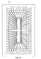
- An example is shown in FIGS. 6A though 6 C, in which an IC assembly 600 has a sixteen-bit driver IC 602 affixed to a leadframe 604 , with forty eight pins 606 requiring wirebonding to the leads 608 of the leadframe 604 .
- the IC 602 includes twelve supply pins 610 , sixteen output pins 612 , and twenty input pins 614 .
- the twenty input pins 614 are preferably wirebonded using one capillary of a bond head, in this case using gold bond wire 616 of approximately 0.6 mils in diameter in order to provide the capability of carrying up to approximately 18 mA of current.
- the output 612 and supply pins 610 are preferably wirebonded with 1.3 mil diameter gold bond wires 618 using the other capillary of the bond head.
- the resulting wirebonded IC assembly 620 shown in FIG. 6C prepared for encapsulation into an IC package, thus realizes a nearly one-third reduction in gold bond wire content compared to methods for using one wire gauge.
- the invention may be used with numerous types of IC assemblies with particular advantages in assemblies in which it is desirable to use wires of different sizes or composition. To cite a few more examples, the advantages of the invention may also be exploited further by using wires of different compositions according to application requirements, such as, gold and copper, or various alloys (e.g., different levels of gold purity), or combinations of insulated and un-insulated wires.
- an IC package assembly may be partitioned into two bond wire groups, such as a small bond wire group and a large bond wire group, or one alloy group and another, or insulated and un-insulated bond wires.
- the different wirebonds may be made without significantly slowing throughput compared to common single bond head techniques, and significant advantages may be realized in terms of reducing precious metal content. Further advantages may be realized in packages for which the IC dimensions are influenced by the minimum bond pad size. In some cases, using the invention to reduce bond wire sizes for some of the bond pads may enable the use of smaller bond pads spaced more closely. As a result, smaller ICs and smaller packages may in turn be realized by implementing the invention.
- a conventional dual bond head approach for producing the IC assembly 620 of FIG. 6C would introduce a workload imbalance; the bond head installing the twenty smaller bond wires would run continuously while the bond head installing the larger bond wires would remain idle during the time that four of the small bond wires were being bonded.
- the greater the disparity in the number of each type of bond wire required the greater the inefficiency.
- the nonproductive bond head time is limited to the minimal time required to rotate the horn in order to change the active capillary.
- the invention provides further new and unique aspects of improved work flow in wirebonding processes, such as that denominated “interlaced” wirebonding herein. It has been determined during the course of developing the invention, that by using two rotatable ultrasonic horn bond head assemblies in a dual bond head configuration, additional advantages may be obtained.
- FIG. 7 an example of dual capillary, dual bond head, interlaced wirebonding according to the invention is shown.
- the workflow 700 in a preferred embodiment of an interlaced bonding method is shown in terms of three time slots 702 , 704 , 706 for showing the progression of the process.
- the activities of two dual capillary bond heads 708 , 710 may be seen as follows.
- each dual capillary bond head possesses the capability of installing both wire gauges, as further described herein, each dual capillary bond head is preferably used to perform alternating small wire and large wire bonds while indexing from one IC assembly to another, e.g., from IC assembly 712 , to IC assembly 714 .
- both bond heads, 708 , 710 perform identical bonding operations at any given time.
- the first bond head 708 is brought to bear on the first IC assembly 712 .
- the first bond head 708 initially installs bond wires of a first gauge 716 , for example large output wires, on the first IC chip 718 , then a bond wire of a second gauge 720 , e.g., a reference pin bond with a single small wire, on the next IC 722 , and alternately repeating this sequence thereafter.
- the second bond head 710 remains idle.
- the first bond head 708 alternately installs bond wires of two gauges 716 , 720 on a second IC assembly 714 , but in this example, in reverse order compared to the sequence it used in the first time slot 702 .
- the second bond head 710 preferably performs identical operations on the first IC assembly 712 , alternately bonding large wires 716 ′ and small wires 720 ′ at the bond targets bypassed by the first bond head 708 during the previous timeslot 702 .
- the first IC assembly 712 has now been completed and may be ejected, as indicted by arrow 722 , for further manufacturing processes such as encapsulation, and the second IC assembly 714 takes its position for further bonding by the second bond head 710 .
- a third IC assembly 724 is moved into a position accessible to the first bond head 708 .
- the first bond head 708 completes large wire 716 and small wire 720 bonds on the third IC assembly 724 .
- the second bond head 710 completes the wire bonds 716 ′, 720 ′ on the second IC assembly 714 , but in an order opposite to the previous, i.e., second, time slot 704 sequence.
- interlaced wirebonding may be used to provide balanced throughput wirebonding workloads with any combination of differing wire sizes, wire compositions, and pin counts. It should be noted that the changes between capillaries of the dual capillary bond heads are preferably performed during the transport index, or x-y table move to an adjacent IC, making such changes transparent to throughput.
Abstract
Description
Claims (11)
Priority Applications (2)
| Application Number | Priority Date | Filing Date | Title |
|---|---|---|---|
| US11/867,228 US8008183B2 (en) | 2007-10-04 | 2007-10-04 | Dual capillary IC wirebonding |
| US13/187,223 US8225982B2 (en) | 2007-10-04 | 2011-07-20 | Dual capillary IC wirebonding |
Applications Claiming Priority (1)
| Application Number | Priority Date | Filing Date | Title |
|---|---|---|---|
| US11/867,228 US8008183B2 (en) | 2007-10-04 | 2007-10-04 | Dual capillary IC wirebonding |
Related Child Applications (1)
| Application Number | Title | Priority Date | Filing Date |
|---|---|---|---|
| US13/187,223 Division US8225982B2 (en) | 2007-10-04 | 2011-07-20 | Dual capillary IC wirebonding |
Publications (2)
| Publication Number | Publication Date |
|---|---|
| US20090091006A1 US20090091006A1 (en) | 2009-04-09 |
| US8008183B2 true US8008183B2 (en) | 2011-08-30 |
Family
ID=40522552
Family Applications (2)
| Application Number | Title | Priority Date | Filing Date |
|---|---|---|---|
| US11/867,228 Active 2029-08-19 US8008183B2 (en) | 2007-10-04 | 2007-10-04 | Dual capillary IC wirebonding |
| US13/187,223 Active US8225982B2 (en) | 2007-10-04 | 2011-07-20 | Dual capillary IC wirebonding |
Family Applications After (1)
| Application Number | Title | Priority Date | Filing Date |
|---|---|---|---|
| US13/187,223 Active US8225982B2 (en) | 2007-10-04 | 2011-07-20 | Dual capillary IC wirebonding |
Country Status (1)
| Country | Link |
|---|---|
| US (2) | US8008183B2 (en) |
Families Citing this family (52)
| Publication number | Priority date | Publication date | Assignee | Title |
|---|---|---|---|---|
| CN101053079A (en) | 2004-11-03 | 2007-10-10 | 德塞拉股份有限公司 | Stacked packaging improvements |
| US8058101B2 (en) | 2005-12-23 | 2011-11-15 | Tessera, Inc. | Microelectronic packages and methods therefor |
| US8459530B2 (en) * | 2009-10-29 | 2013-06-11 | Asm Technology Singapore Pte Ltd | Automatic wire feeding method for wire bonders |
| US9159708B2 (en) | 2010-07-19 | 2015-10-13 | Tessera, Inc. | Stackable molded microelectronic packages with area array unit connectors |
| US8482111B2 (en) | 2010-07-19 | 2013-07-09 | Tessera, Inc. | Stackable molded microelectronic packages |
| KR101075241B1 (en) | 2010-11-15 | 2011-11-01 | 테세라, 인코포레이티드 | Microelectronic package with terminals on dielectric mass |
| US20120146206A1 (en) | 2010-12-13 | 2012-06-14 | Tessera Research Llc | Pin attachment |
| KR101128063B1 (en) | 2011-05-03 | 2012-04-23 | 테세라, 인코포레이티드 | Package-on-package assembly with wire bonds to encapsulation surface |
| US8618659B2 (en) | 2011-05-03 | 2013-12-31 | Tessera, Inc. | Package-on-package assembly with wire bonds to encapsulation surface |
| US8404520B1 (en) | 2011-10-17 | 2013-03-26 | Invensas Corporation | Package-on-package assembly with wire bond vias |
| US8946757B2 (en) | 2012-02-17 | 2015-02-03 | Invensas Corporation | Heat spreading substrate with embedded interconnects |
| US9349706B2 (en) | 2012-02-24 | 2016-05-24 | Invensas Corporation | Method for package-on-package assembly with wire bonds to encapsulation surface |
| US8372741B1 (en) | 2012-02-24 | 2013-02-12 | Invensas Corporation | Method for package-on-package assembly with wire bonds to encapsulation surface |
| US8835228B2 (en) | 2012-05-22 | 2014-09-16 | Invensas Corporation | Substrate-less stackable package with wire-bond interconnect |
| US9391008B2 (en) | 2012-07-31 | 2016-07-12 | Invensas Corporation | Reconstituted wafer-level package DRAM |
| US9502390B2 (en) | 2012-08-03 | 2016-11-22 | Invensas Corporation | BVA interposer |
| US8975738B2 (en) | 2012-11-12 | 2015-03-10 | Invensas Corporation | Structure for microelectronic packaging with terminals on dielectric mass |
| US8878353B2 (en) | 2012-12-20 | 2014-11-04 | Invensas Corporation | Structure for microelectronic packaging with bond elements to encapsulation surface |
| US8767351B1 (en) * | 2013-01-31 | 2014-07-01 | Seagate Technology Llc | Ambient temperature ball bond |
| US9136254B2 (en) | 2013-02-01 | 2015-09-15 | Invensas Corporation | Microelectronic package having wire bond vias and stiffening layer |
| US9034696B2 (en) | 2013-07-15 | 2015-05-19 | Invensas Corporation | Microelectronic assemblies having reinforcing collars on connectors extending through encapsulation |
| US8883563B1 (en) | 2013-07-15 | 2014-11-11 | Invensas Corporation | Fabrication of microelectronic assemblies having stack terminals coupled by connectors extending through encapsulation |
| US9023691B2 (en) | 2013-07-15 | 2015-05-05 | Invensas Corporation | Microelectronic assemblies with stack terminals coupled by connectors extending through encapsulation |
| US9167710B2 (en) | 2013-08-07 | 2015-10-20 | Invensas Corporation | Embedded packaging with preformed vias |
| US9685365B2 (en) | 2013-08-08 | 2017-06-20 | Invensas Corporation | Method of forming a wire bond having a free end |
| US20150076714A1 (en) | 2013-09-16 | 2015-03-19 | Invensas Corporation | Microelectronic element with bond elements to encapsulation surface |
| US9082753B2 (en) | 2013-11-12 | 2015-07-14 | Invensas Corporation | Severing bond wire by kinking and twisting |
| US9087815B2 (en) | 2013-11-12 | 2015-07-21 | Invensas Corporation | Off substrate kinking of bond wire |
| US9583456B2 (en) | 2013-11-22 | 2017-02-28 | Invensas Corporation | Multiple bond via arrays of different wire heights on a same substrate |
| US9379074B2 (en) | 2013-11-22 | 2016-06-28 | Invensas Corporation | Die stacks with one or more bond via arrays of wire bond wires and with one or more arrays of bump interconnects |
| US9263394B2 (en) | 2013-11-22 | 2016-02-16 | Invensas Corporation | Multiple bond via arrays of different wire heights on a same substrate |
| US9583411B2 (en) | 2014-01-17 | 2017-02-28 | Invensas Corporation | Fine pitch BVA using reconstituted wafer with area array accessible for testing |
| US9214454B2 (en) | 2014-03-31 | 2015-12-15 | Invensas Corporation | Batch process fabrication of package-on-package microelectronic assemblies |
| US10381326B2 (en) | 2014-05-28 | 2019-08-13 | Invensas Corporation | Structure and method for integrated circuits packaging with increased density |
| US9646917B2 (en) | 2014-05-29 | 2017-05-09 | Invensas Corporation | Low CTE component with wire bond interconnects |
| US9412714B2 (en) | 2014-05-30 | 2016-08-09 | Invensas Corporation | Wire bond support structure and microelectronic package including wire bonds therefrom |
| US9165904B1 (en) * | 2014-06-17 | 2015-10-20 | Freescale Semiconductor, Inc. | Insulated wire bonding with EFO before second bond |
| US9735084B2 (en) | 2014-12-11 | 2017-08-15 | Invensas Corporation | Bond via array for thermal conductivity |
| US9888579B2 (en) | 2015-03-05 | 2018-02-06 | Invensas Corporation | Pressing of wire bond wire tips to provide bent-over tips |
| US9502372B1 (en) | 2015-04-30 | 2016-11-22 | Invensas Corporation | Wafer-level packaging using wire bond wires in place of a redistribution layer |
| US9761554B2 (en) | 2015-05-07 | 2017-09-12 | Invensas Corporation | Ball bonding metal wire bond wires to metal pads |
| US9490222B1 (en) | 2015-10-12 | 2016-11-08 | Invensas Corporation | Wire bond wires for interference shielding |
| US10490528B2 (en) | 2015-10-12 | 2019-11-26 | Invensas Corporation | Embedded wire bond wires |
| US10332854B2 (en) | 2015-10-23 | 2019-06-25 | Invensas Corporation | Anchoring structure of fine pitch bva |
| US10181457B2 (en) | 2015-10-26 | 2019-01-15 | Invensas Corporation | Microelectronic package for wafer-level chip scale packaging with fan-out |
| US9911718B2 (en) | 2015-11-17 | 2018-03-06 | Invensas Corporation | ‘RDL-First’ packaged microelectronic device for a package-on-package device |
| US9659848B1 (en) | 2015-11-18 | 2017-05-23 | Invensas Corporation | Stiffened wires for offset BVA |
| US9984992B2 (en) | 2015-12-30 | 2018-05-29 | Invensas Corporation | Embedded wire bond wires for vertical integration with separate surface mount and wire bond mounting surfaces |
| US9935075B2 (en) | 2016-07-29 | 2018-04-03 | Invensas Corporation | Wire bonding method and apparatus for electromagnetic interference shielding |
| US10299368B2 (en) | 2016-12-21 | 2019-05-21 | Invensas Corporation | Surface integrated waveguides and circuit structures therefor |
| WO2019232718A1 (en) | 2018-06-06 | 2019-12-12 | Texas Instruments Incorporated | Ball bond attachment for semiconductor die |
| WO2021155537A1 (en) | 2020-02-06 | 2021-08-12 | Texas Instruments Incorporated | Copper wire bond on gold bump on semiconductor die bond pad |
Citations (41)
| Publication number | Priority date | Publication date | Assignee | Title |
|---|---|---|---|---|
| US3641660A (en) * | 1969-06-30 | 1972-02-15 | Texas Instruments Inc | The method of ball bonding with an automatic semiconductor bonding machine |
| US3781613A (en) * | 1972-10-10 | 1973-12-25 | Collins Radio Co | Rf transistor carrier |
| US3780926A (en) * | 1972-06-02 | 1973-12-25 | Dukane Corp | Ultrasonic rigid horn assembly |
| US3840169A (en) * | 1971-01-27 | 1974-10-08 | Inforex | Automatic bonding apparatus with multiple bonding heads |
| US4142288A (en) * | 1976-02-28 | 1979-03-06 | Licentia Patent-Verwaltungs-G.M.B.H. | Method for contacting contact areas located on semiconductor bodies |
| JPS6178133A (en) * | 1984-09-25 | 1986-04-21 | Toshiba Corp | Wire bonding device |
| GB2177639A (en) * | 1985-07-08 | 1987-01-28 | Philips Electronic Associated | Ultrasonic wire bonder and method of manufacturing a semiconductor therewith |
| JPS62156828A (en) * | 1985-12-28 | 1987-07-11 | Toshiba Corp | Wire bonding device |
| JPS62176138A (en) * | 1986-01-29 | 1987-08-01 | Toshiba Corp | Wire bonding device |
| JPS6328043A (en) * | 1986-07-21 | 1988-02-05 | Nec Yamagata Ltd | Wire bonding apparatus |
| US4860433A (en) * | 1984-10-18 | 1989-08-29 | Sanyo Electric Co., Ltd. | Method of manufacturing an inductance element |
| JPH0228339A (en) * | 1988-07-18 | 1990-01-30 | Mitsubishi Electric Corp | Method and apparatus for wire bonding |
| US5080276A (en) | 1989-03-27 | 1992-01-14 | Kabushiki Kaisha Toshiba | Motor-driving circuit and wire-bonding apparatus |
| US5110032A (en) * | 1988-11-28 | 1992-05-05 | Hitachi, Ltd., | Method and apparatus for wire bonding |
| JPH04267353A (en) * | 1991-02-22 | 1992-09-22 | Hitachi Ltd | Wire bonder |
| US5201454A (en) * | 1991-09-30 | 1993-04-13 | Texas Instruments Incorporated | Process for enhanced intermetallic growth in IC interconnections |
| JPH05102223A (en) * | 1991-10-07 | 1993-04-23 | Seiko Epson Corp | Manufacture of semiconductor device |
| JPH05102232A (en) * | 1991-10-07 | 1993-04-23 | Seiko Epson Corp | Semiconductor manufacturing device |
| JPH0653268A (en) * | 1992-07-31 | 1994-02-25 | Nec Corp | Wire bonding device |
| US5544804A (en) * | 1994-06-08 | 1996-08-13 | Texas Instruments Incorporated | Capillary designs and process for fine pitch ball bonding |
| JPH0945717A (en) * | 1995-05-22 | 1997-02-14 | Rohm Co Ltd | Wire bonding method and capillary used for it |
| US5839640A (en) * | 1996-10-23 | 1998-11-24 | Texas Instruments Incorporated | Multiple-tool wire bonder |
| US5904288A (en) * | 1996-04-08 | 1999-05-18 | Texas Instruments Incorporated | Wire bond clamping method |
| US5944249A (en) * | 1996-12-12 | 1999-08-31 | Texas Instruments Incorporated | Wire bonding capillary with bracing component |
| US5947364A (en) * | 1995-10-20 | 1999-09-07 | Harness System Technologies Research, Ltd. | Ultrasonic welding apparatus |
| US5979743A (en) * | 1994-06-08 | 1999-11-09 | Texas Instruments Incorporated | Method for making an IC device using a single-headed bonder |
| US6112973A (en) * | 1997-10-31 | 2000-09-05 | Texas Instruments Incorporated | Angled transducer-dual head bonder for optimum ultrasonic power application and flexibility for tight pitch leadframe |
| US6322659B1 (en) * | 1998-07-24 | 2001-11-27 | Texas Instruments Incorporated | System and method for dual head bonding |
| KR20020057253A (en) * | 2000-12-30 | 2002-07-11 | 박종섭 | An apparatus for multi-bonding of wire |
| US6564115B1 (en) * | 2000-02-01 | 2003-05-13 | Texas Instruments Incorporated | Combined system, method and apparatus for wire bonding and testing |
| US20030098333A1 (en) | 2001-11-27 | 2003-05-29 | Nec Corporation | Wire bonding device and wire bonding method |
| US6749100B2 (en) * | 2001-11-28 | 2004-06-15 | Asm Technology Singapore Pte Ltd. | Multiple-head wire-bonding system |
| US20050051600A1 (en) * | 2003-09-10 | 2005-03-10 | Texas Instruments Incorporated | Method and system for stud bumping |
| KR20060094438A (en) * | 2005-02-24 | 2006-08-29 | 삼성테크윈 주식회사 | Ultrasonic transducer for wire bonding |
| US20070000878A1 (en) * | 2005-06-30 | 2007-01-04 | Kabushiki Kaisha Shinkawa | Bonding apparatus and method |
| US20070228110A1 (en) * | 1993-11-16 | 2007-10-04 | Formfactor, Inc. | Method Of Wirebonding That Utilizes A Gas Flow Within A Capillary From Which A Wire Is Played Out |
| US7320423B2 (en) * | 2002-11-19 | 2008-01-22 | Kulicke And Soffa Industries, Inc. | High speed linear and rotary split-axis wire bonder |
| US20080035706A1 (en) * | 2006-08-14 | 2008-02-14 | Advanced Semiconductor Engineering, Inc. | Wire-bonding apparatus and wire-bonding method thereof |
| US7371675B2 (en) * | 2004-03-11 | 2008-05-13 | Samsung Electronics Co., Ltd. | Method and apparatus for bonding a wire |
| US7568606B2 (en) * | 2006-10-19 | 2009-08-04 | Asm Technology Singapore Pte Ltd. | Electronic device handler for a bonding apparatus |
| US7677431B2 (en) * | 2006-10-19 | 2010-03-16 | Asm Technology Singapore Pte Ltd. | Electronic device handler for a bonding apparatus |
Family Cites Families (1)
| Publication number | Priority date | Publication date | Assignee | Title |
|---|---|---|---|---|
| KR20080067518A (en) | 2007-01-16 | 2008-07-21 | 삼성전자주식회사 | Apparatus and method for wirebonding |
-
2007
- 2007-10-04 US US11/867,228 patent/US8008183B2/en active Active
-
2011
- 2011-07-20 US US13/187,223 patent/US8225982B2/en active Active
Patent Citations (43)
| Publication number | Priority date | Publication date | Assignee | Title |
|---|---|---|---|---|
| US3641660A (en) * | 1969-06-30 | 1972-02-15 | Texas Instruments Inc | The method of ball bonding with an automatic semiconductor bonding machine |
| US3840169A (en) * | 1971-01-27 | 1974-10-08 | Inforex | Automatic bonding apparatus with multiple bonding heads |
| US3780926A (en) * | 1972-06-02 | 1973-12-25 | Dukane Corp | Ultrasonic rigid horn assembly |
| US3781613A (en) * | 1972-10-10 | 1973-12-25 | Collins Radio Co | Rf transistor carrier |
| US4142288A (en) * | 1976-02-28 | 1979-03-06 | Licentia Patent-Verwaltungs-G.M.B.H. | Method for contacting contact areas located on semiconductor bodies |
| JPS6178133A (en) * | 1984-09-25 | 1986-04-21 | Toshiba Corp | Wire bonding device |
| US4860433A (en) * | 1984-10-18 | 1989-08-29 | Sanyo Electric Co., Ltd. | Method of manufacturing an inductance element |
| GB2177639A (en) * | 1985-07-08 | 1987-01-28 | Philips Electronic Associated | Ultrasonic wire bonder and method of manufacturing a semiconductor therewith |
| JPS62156828A (en) * | 1985-12-28 | 1987-07-11 | Toshiba Corp | Wire bonding device |
| US4765526A (en) * | 1986-01-29 | 1988-08-23 | Kabushiki Kaisha Toshiba | Wire bonding apparatus |
| JPS62176138A (en) * | 1986-01-29 | 1987-08-01 | Toshiba Corp | Wire bonding device |
| JPS6328043A (en) * | 1986-07-21 | 1988-02-05 | Nec Yamagata Ltd | Wire bonding apparatus |
| JPH0228339A (en) * | 1988-07-18 | 1990-01-30 | Mitsubishi Electric Corp | Method and apparatus for wire bonding |
| US5110032A (en) * | 1988-11-28 | 1992-05-05 | Hitachi, Ltd., | Method and apparatus for wire bonding |
| US5080276A (en) | 1989-03-27 | 1992-01-14 | Kabushiki Kaisha Toshiba | Motor-driving circuit and wire-bonding apparatus |
| JPH04267353A (en) * | 1991-02-22 | 1992-09-22 | Hitachi Ltd | Wire bonder |
| US5201454A (en) * | 1991-09-30 | 1993-04-13 | Texas Instruments Incorporated | Process for enhanced intermetallic growth in IC interconnections |
| JPH05102223A (en) * | 1991-10-07 | 1993-04-23 | Seiko Epson Corp | Manufacture of semiconductor device |
| JPH05102232A (en) * | 1991-10-07 | 1993-04-23 | Seiko Epson Corp | Semiconductor manufacturing device |
| JPH0653268A (en) * | 1992-07-31 | 1994-02-25 | Nec Corp | Wire bonding device |
| US20070228110A1 (en) * | 1993-11-16 | 2007-10-04 | Formfactor, Inc. | Method Of Wirebonding That Utilizes A Gas Flow Within A Capillary From Which A Wire Is Played Out |
| US5544804A (en) * | 1994-06-08 | 1996-08-13 | Texas Instruments Incorporated | Capillary designs and process for fine pitch ball bonding |
| US5979743A (en) * | 1994-06-08 | 1999-11-09 | Texas Instruments Incorporated | Method for making an IC device using a single-headed bonder |
| JPH0945717A (en) * | 1995-05-22 | 1997-02-14 | Rohm Co Ltd | Wire bonding method and capillary used for it |
| US5947364A (en) * | 1995-10-20 | 1999-09-07 | Harness System Technologies Research, Ltd. | Ultrasonic welding apparatus |
| US5904288A (en) * | 1996-04-08 | 1999-05-18 | Texas Instruments Incorporated | Wire bond clamping method |
| US5839640A (en) * | 1996-10-23 | 1998-11-24 | Texas Instruments Incorporated | Multiple-tool wire bonder |
| US5944249A (en) * | 1996-12-12 | 1999-08-31 | Texas Instruments Incorporated | Wire bonding capillary with bracing component |
| US6112973A (en) * | 1997-10-31 | 2000-09-05 | Texas Instruments Incorporated | Angled transducer-dual head bonder for optimum ultrasonic power application and flexibility for tight pitch leadframe |
| US6182882B1 (en) * | 1997-10-31 | 2001-02-06 | Texas Instruments Incorporated | Angled transducer-dual head bonder for optimum ultrasonic power application and flexibility for tight pitch leadframe |
| US6322659B1 (en) * | 1998-07-24 | 2001-11-27 | Texas Instruments Incorporated | System and method for dual head bonding |
| US6564115B1 (en) * | 2000-02-01 | 2003-05-13 | Texas Instruments Incorporated | Combined system, method and apparatus for wire bonding and testing |
| KR20020057253A (en) * | 2000-12-30 | 2002-07-11 | 박종섭 | An apparatus for multi-bonding of wire |
| US20030098333A1 (en) | 2001-11-27 | 2003-05-29 | Nec Corporation | Wire bonding device and wire bonding method |
| US6749100B2 (en) * | 2001-11-28 | 2004-06-15 | Asm Technology Singapore Pte Ltd. | Multiple-head wire-bonding system |
| US7320423B2 (en) * | 2002-11-19 | 2008-01-22 | Kulicke And Soffa Industries, Inc. | High speed linear and rotary split-axis wire bonder |
| US20050051600A1 (en) * | 2003-09-10 | 2005-03-10 | Texas Instruments Incorporated | Method and system for stud bumping |
| US7371675B2 (en) * | 2004-03-11 | 2008-05-13 | Samsung Electronics Co., Ltd. | Method and apparatus for bonding a wire |
| KR20060094438A (en) * | 2005-02-24 | 2006-08-29 | 삼성테크윈 주식회사 | Ultrasonic transducer for wire bonding |
| US20070000878A1 (en) * | 2005-06-30 | 2007-01-04 | Kabushiki Kaisha Shinkawa | Bonding apparatus and method |
| US20080035706A1 (en) * | 2006-08-14 | 2008-02-14 | Advanced Semiconductor Engineering, Inc. | Wire-bonding apparatus and wire-bonding method thereof |
| US7568606B2 (en) * | 2006-10-19 | 2009-08-04 | Asm Technology Singapore Pte Ltd. | Electronic device handler for a bonding apparatus |
| US7677431B2 (en) * | 2006-10-19 | 2010-03-16 | Asm Technology Singapore Pte Ltd. | Electronic device handler for a bonding apparatus |
Non-Patent Citations (1)
| Title |
|---|
| Derwent English abstract and one clipped image from KrR724065 B1, Apr. 6, 2007, pgs. * |
Also Published As
| Publication number | Publication date |
|---|---|
| US20090091006A1 (en) | 2009-04-09 |
| US20110272449A1 (en) | 2011-11-10 |
| US8225982B2 (en) | 2012-07-24 |
Similar Documents
| Publication | Publication Date | Title |
|---|---|---|
| US8008183B2 (en) | Dual capillary IC wirebonding | |
| US6774494B2 (en) | Semiconductor device and manufacturing method thereof | |
| JPH08181162A (en) | Method and equipment for doing wire bonding of pitch that issmall by using shaved capillary | |
| US4527730A (en) | Wire bonding apparatus | |
| KR20050023972A (en) | Wire bonding method of semiconductor device | |
| JP2007535820A (en) | Low loop wire bonding systems and methods | |
| US6564989B2 (en) | Wire bonding method and wire bonding apparatus | |
| US5153981A (en) | Universal apparatus for forming lead wires | |
| US20090078743A1 (en) | Wire bonding system utilizing multiple positioning tables | |
| WO2010042117A1 (en) | Dual capillary wirebonding | |
| JPH0917819A (en) | Connection method in manufacturing of microelectronics device | |
| WO2005018864A2 (en) | Capillary with contained inner chamfer | |
| US7159751B2 (en) | Wire bonder | |
| US20050200009A1 (en) | Method and apparatus for bonding a wire | |
| TWI435396B (en) | Dual capillary icwirebonding | |
| WO2008048262A1 (en) | Improved conductive bumps, wire loops including the improved conductive bumps, and methods of forming the same | |
| US6006981A (en) | Wirefilm bonding for electronic component interconnection | |
| CN1678424A (en) | Wedge-bonding of wires in electronic device manufacture with a reversible wedge bonding tool | |
| JP2007012642A (en) | Wire bonding method | |
| JP2500655B2 (en) | Wire-bonding method and device | |
| WO2009148450A1 (en) | Bonding tool with improved working face | |
| US20110121053A1 (en) | Z-axis motion system for a wire bonding machine | |
| US11289446B2 (en) | Multiple actuator wire bonding apparatus | |
| JP3363812B2 (en) | Semiconductor device, wire bonding method for the semiconductor device, and wire bonder | |
| JPH10125710A (en) | Wire bonding |
Legal Events
| Date | Code | Title | Description |
|---|---|---|---|
| AS | Assignment |
Owner name: TEXAS INSTRUMENTS INCORPORATED, TEXAS Free format text: ASSIGNMENT OF ASSIGNORS INTEREST;ASSIGNORS:PIRKLE, REX WARREN;MALOLEPSZY, SEAN MICHAEL;BON, DAVID JOSEPH;REEL/FRAME:020081/0201;SIGNING DATES FROM 20071029 TO 20071030 Owner name: TEXAS INSTRUMENTS INCORPORATED, TEXAS Free format text: ASSIGNMENT OF ASSIGNORS INTEREST;ASSIGNORS:PIRKLE, REX WARREN;MALOLEPSZY, SEAN MICHAEL;BON, DAVID JOSEPH;SIGNING DATES FROM 20071029 TO 20071030;REEL/FRAME:020081/0201 |
|
| STCF | Information on status: patent grant |
Free format text: PATENTED CASE |
|
| FPAY | Fee payment |
Year of fee payment: 4 |
|
| MAFP | Maintenance fee payment |
Free format text: PAYMENT OF MAINTENANCE FEE, 8TH YEAR, LARGE ENTITY (ORIGINAL EVENT CODE: M1552); ENTITY STATUS OF PATENT OWNER: LARGE ENTITY Year of fee payment: 8 |
|
| MAFP | Maintenance fee payment |
Free format text: PAYMENT OF MAINTENANCE FEE, 12TH YEAR, LARGE ENTITY (ORIGINAL EVENT CODE: M1553); ENTITY STATUS OF PATENT OWNER: LARGE ENTITY Year of fee payment: 12 |