US8023319B2 - Phase change memory - Google Patents

Phase change memory Download PDF

Info

Publication number
US8023319B2
US8023319B2 US12/457,319 US45731909A US8023319B2 US 8023319 B2 US8023319 B2 US 8023319B2 US 45731909 A US45731909 A US 45731909A US 8023319 B2 US8023319 B2 US 8023319B2
Authority
US
United States
Prior art keywords
local
global
redundant
address
conductor line
Prior art date
Legal status (The legal status is an assumption and is not a legal conclusion. Google has not performed a legal analysis and makes no representation as to the accuracy of the status listed.)
Expired - Fee Related, expires
Application number
US12/457,319
Other versions
US20090316474A1 (en
Inventor
Beak-Hyung Cho
Byung-Gil Choi
Joon-Min Park
Current Assignee (The listed assignees may be inaccurate. Google has not performed a legal analysis and makes no representation or warranty as to the accuracy of the list.)
Samsung Electronics Co Ltd
Original Assignee
Samsung Electronics Co Ltd
Priority date (The priority date is an assumption and is not a legal conclusion. Google has not performed a legal analysis and makes no representation as to the accuracy of the date listed.)
Filing date
Publication date
Application filed by Samsung Electronics Co Ltd filed Critical Samsung Electronics Co Ltd
Assigned to SAMSUNG ELECTRONICS CO., LTD. reassignment SAMSUNG ELECTRONICS CO., LTD. ASSIGNMENT OF ASSIGNORS INTEREST (SEE DOCUMENT FOR DETAILS). Assignors: CHO, BEAK-HYUNG, CHOI, BYUNG-GIL, PARK, JOON-MIN
Publication of US20090316474A1 publication Critical patent/US20090316474A1/en
Application granted granted Critical
Publication of US8023319B2 publication Critical patent/US8023319B2/en
Expired - Fee Related legal-status Critical Current
Adjusted expiration legal-status Critical

Links

Images

Classifications

    • GPHYSICS
    • G11INFORMATION STORAGE
    • G11CSTATIC STORES
    • G11C29/00Checking stores for correct operation ; Subsequent repair; Testing stores during standby or offline operation
    • G11C29/70Masking faults in memories by using spares or by reconfiguring
    • G11C29/78Masking faults in memories by using spares or by reconfiguring using programmable devices
    • G11C29/80Masking faults in memories by using spares or by reconfiguring using programmable devices with improved layout
    • G11C29/808Masking faults in memories by using spares or by reconfiguring using programmable devices with improved layout using a flexible replacement scheme
    • GPHYSICS
    • G11INFORMATION STORAGE
    • G11CSTATIC STORES
    • G11C13/00Digital stores characterised by the use of storage elements not covered by groups G11C11/00, G11C23/00, or G11C25/00
    • G11C13/0002Digital stores characterised by the use of storage elements not covered by groups G11C11/00, G11C23/00, or G11C25/00 using resistive RAM [RRAM] elements
    • G11C13/0004Digital stores characterised by the use of storage elements not covered by groups G11C11/00, G11C23/00, or G11C25/00 using resistive RAM [RRAM] elements comprising amorphous/crystalline phase transition cells
    • HELECTRICITY
    • H10SEMICONDUCTOR DEVICES; ELECTRIC SOLID-STATE DEVICES NOT OTHERWISE PROVIDED FOR
    • H10NELECTRIC SOLID-STATE DEVICES NOT OTHERWISE PROVIDED FOR
    • H10N70/00Solid-state devices without a potential-jump barrier or surface barrier, and specially adapted for rectifying, amplifying, oscillating or switching
    • H10N70/20Multistable switching devices, e.g. memristors
    • H10N70/231Multistable switching devices, e.g. memristors based on solid-state phase change, e.g. between amorphous and crystalline phases, Ovshinsky effect

Definitions

  • Example embodiments of the present invention relate to a semiconductor memory device, for example, to a phase change memory device.
  • a semiconductor memory device is a memory device that stores data and from which stored data may be read.
  • the semiconductor memory device may be divided into a volatile memory device and a nonvolatile memory device.
  • the volatile memory device is a memory device in which retained data is erased when a power supply is cut off. Some examples of the volatile memory device are SRAM, DRAM and SDRAM.
  • the nonvolatile memory device is a memory device in which retained data is not erased even when power supply is cut off. Some examples of the nonvolatile memory device are ROM, PROM, EPROM, EEPROM, flash memory device, PRAM, MRAM, RRAM, and FRAM.
  • a phase change memory is a memory device that stores data using a material of which a resistance varies with temperature, for example, chalcogenide.
  • a temperature higher than the melting point of chalcogenide is applied to the chalcogenide for a relatively shorter period of time, the chalcogenide becomes an amorphous state.
  • a temperature lower than the melting point of chalcogenide is applied to the chalcogenide for a longer period of time, the chalcogenide becomes a crystalline state.
  • a resistance of the chalcogenide in the crystalline state is lower than a resistance of the chalcogenide in the amorphous state.
  • the phase change memory device may store data by changing chalcogenide into a crystalline state or an amorphous state.
  • a phase change memory device includes a plurality of memory banks, a plurality of local conductor lines connected to the plurality of memory banks, at least one global conductor line connected to the plurality of local conductor lines, and at least one repair control circuit configured to selectively replace at least one of the at least one global conductor line with at least one redundant global conductor line and configured to selectively replace at least one of the plurality of local conductor lines with at least one redundant local conductor line.
  • a phase change memory device includes a plurality of memory banks each including a plurality of address groups and at least one redundant address group, a plurality of local conductor lines connected to each of the address groups and at least one redundant local conductor line connected to the at least one redundant address group, at least one global conductor line connected to the plurality of local conductor lines of each of the address groups, at least one redundant global conductor line connected to the at least redundant local conductor line of the at least one redundant address group, and at least one repair control circuit configured to selectively replace at least one of the at least one global conductor line with the at least one redundant global conductor line and configured to selectively replace at least one of the plurality of local conductor lines with the at least one redundant local conductor line.
  • a phase change memory device includes at least one global conductor line connected to a plurality of local conductor lines, and at least one repair control circuit configured to selectively replace at least one of the at least one global conductor line with at least one redundant global conductor line and configured to selectively replace at least one of the plurality of local conductor lines with at least one redundant local conductor line
  • the at least one repair control circuit includes a master repair circuit including a plurality of fuses corresponding to the at least one global conductor line and receiving a column address, where the master repair circuit activates a first active signal in response to an output of at least one of the plurality of fuses of the master repair circuit, a first slave repair circuit including a plurality of fuses corresponding to a plurality of memory banks and receiving a bank address, where the first slave repair circuit activates a second active signal in response to an output of at least one of the plurality of fuses of the first slave repair circuit, and a second slave repair circuit including a plurality of fuses corresponding to the plurality
  • An example embodiment may further include a controller that controls the phase change memory device.
  • FIG. 1 is a block diagram depicting a memory system according to an example embodiment of the present invention
  • FIG. 2 is a block diagram depicting an example embodiment of the phase change memory device of FIG. 1 ;
  • FIG. 3 is a block diagram depicting memory banks of the memory cell array of FIG. 2 ;
  • FIG. 4 is a circuit diagram depicting address groups of FIG. 3 ;
  • FIG. 5A is a block diagram depicting an example embodiment of a repair control circuit shown in FIGS. 2 and 3 ;
  • FIG. 5B is a block diagram depicting an example embodiment of a master repair circuit shown in FIG. 5A ;
  • FIG. 5C is a block diagram depicting an example embodiment of a first slave repair circuit shown in FIG. 5A ;
  • FIG. 5D is a block diagram depicting an example embodiment of a second slave repair circuit shown in FIG. 5A ;
  • FIG. 5E is a diagram depicting an example embodiment of an output circuit shown in FIG. 5A ;
  • FIGS. 6 to 9 are block diagrams depicting a repairing method according to an example embodiment of the present invention.
  • FIG. 10 is a block diagram depicting one of the memory banks of FIG. 3 ;
  • FIGS. 11 to 13 are block diagrams depicting another repairing method according to an example embodiment of the present invention.
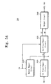
  • FIG. 14 is a block diagram depicting a computing system that includes the memory system of FIG. 1 .
  • first, second, third etc. may be used herein to describe various elements, components, regions, layers and/or sections, these elements, components, regions, layers and/or sections should not be limited by these terms. These terms are only used to distinguish one element, component, region, layer or section from another region, layer or section. Thus, a first element, component, region, layer or section discussed below could be termed a second element, component, region, layer or section without departing from the teachings of the present invention.
  • spatially relative terms such as “beneath”, “below”, “bottom”, “lower”, “above”, “top”, “upper” and the like, may be used herein for ease of description to describe one element or feature's relationship to another element(s) or feature(s) as illustrated in the figures. It will be understood that the spatially relative terms are intended to encompass different orientations of the device in use or operation in addition to the orientation depicted in the figures. For example, if the device in the figures is turned over, elements described as “below” or “beneath” other elements or features would then be oriented “above” the other elements or features. Thus, the exemplary term “below” can encompass both an orientation of above and below. The device may be otherwise oriented (rotated 90 degrees or at other orientations) and the spatially relative descriptors used herein interpreted accordingly. Also, as used herein, “lateral” refers to a direction that is substantially orthogonal to a vertical direction.
  • Example embodiments of the present invention are described herein with reference to cross-section illustrations that are schematic illustrations of idealized embodiments (and intermediate structures) of the invention. As such, variations from the shapes of the illustrations as a result, for example, of manufacturing techniques and/or tolerances, are to be expected. Thus, embodiments of the present invention should not be construed as limited to the particular shapes of regions illustrated herein but are to include deviations in shapes that result, for example, from manufacturing. For example, an implanted region illustrated as a rectangle will, typically, have rounded or curved features and/or a gradient of implant concentration at its edges rather than a binary change from implanted to non-implanted region.
  • a buried region formed by implantation may result in some implantation in the region between the buried region and the surface through which the implantation takes place.
  • the regions illustrated in the figures are schematic in nature and their shapes are not intended to illustrate the actual shape of a region of a device and are not intended to limit the scope of the present invention.
  • FIG. 1 is a block diagram depicting a memory system 10 according to an example embodiment of the present invention.
  • the memory system 10 according to an example embodiment of the present invention includes a controller 100 and a phase change memory device 200 .
  • the controller 100 is connected to a host (not shown) and the phase change memory device 200 .
  • the controller 100 transfers data read from the phase change memory device 200 to the host, or stores data transmitted from the host in the phase change memory device 200 .
  • the controller 100 may include a RAM (not shown), a processing unit (not shown), a host interface (not shown), and a memory interface (not shown).
  • the RAM is used as an operation memory of the processing unit.
  • the processing unit controls the entire operations of the controller 100 .
  • the host interface includes a protocol that performs data exchange between the host and the controller 100 .
  • the controller 10 may be configured to communicate with an external device (host) through one of the various interface protocols, for example, a USB, MMC, PCI-E, Advanced Technology Attachment (ATA), Serial-ATA, Parallel-ATA, SCSI, ESDI, and Integrated Drive Electronics (IDE).
  • the memory interface interfaces with a phase change memory device 200 .
  • the controller 100 may further include an error correction block.
  • the error correction block detects and corrects error in the data read from the phase change memory device 200 .
  • the controller 100 and the phase change memory device 200 may be integrated into one semiconductor device.
  • the controller 100 and the phase change memory device 200 are integrated into one semiconductor device to form a memory card.
  • the controller 100 and the phase change memory device 200 may be integrated into one semiconductor device to form a Solid State Disk/Drive (SSD).
  • SSD Solid State Disk/Drive
  • FIG. 2 is a block diagram depicting an example embodiment of the phase change memory device 200 of FIG. 1 .
  • the phase change memory device 200 includes a memory cell array 210 , a column selector 220 , a sense amplifier/write drive circuit 230 , a multiplexer 240 , a data input/output circuit 250 , a row decoder 260 , a column decoder 270 , a repair control circuit 280 , and a control logic 290 .
  • the memory cell array 210 includes a plurality of phase change memory cells (not shown).
  • the phase change memory cells may have a resistance that varies according to an applied temperature.
  • the phase change memory cells may include chalcogenide in which the resistance varies according to the applied temperature.
  • the chalcogenide may change into an amorphous state when a temperature higher than the melting point of the chalcogenide is applied to the chalcogenide for a shorter period of time.
  • the chalcogenide may change into a crystalline state when a temperature lower than the melting point of the chalcogenide is applied to the chalcogenide for a longer period of time.
  • the resistance of the chalcogenide in the crystalline state is lower than the resistance of the chalcogenide in the amorphous state.
  • the phase change memory device may store data by changing the chalcogenide into a crystalline state or an amorphous state.
  • phase change memory cells are connected to bitlines and wordlines formed in a layer structure.
  • bitlines consist of local bitlines and global bitlines
  • wordlines consist of local wordlines and global wordlines.
  • the memory cell array 210 will be described in further detail with reference to FIGS. 3 and 4 .
  • the column selector 220 is connected to the memory cell array 210 via the bitlines.
  • the column selector 220 selects the bitlines in response to a control by the column decoder 270 .
  • the column selector 220 selects redundant bitlines in response to control signals transmitted from the repair control circuit 280 .
  • the selected bitlines/redundant bitlines are electrically connected to the sense amplifier/write drive circuit 230 via the column selector 220 .
  • the sense amplifier/write drive circuit 230 is electrically connected to the selected bitlines by the column selector 220 .
  • the sense amplifier/write drive circuit 230 detects data stored in the memory cell connected to the selected bitline, and writes data in the memory cell connected to the selected bitline.
  • the sense amplifier/write drive circuit 230 includes a plurality of sense amplifiers/write drivers (not shown) and a plurality of redundant sense amplifier/write drivers (not shown).
  • the respective sense amplifier/write drivers and the respective redundant sense amplifier/write drivers sense data stored in the memory cell that is connected to the corresponding bitline/redundant bitline, or sense write data in the memory cell connected to the corresponding bitline.
  • the sense amplifier/write drive circuit 230 is connected to the multiplexer 240 .
  • the multiplexer 240 selects sense amplifier/write drivers of the sense amplifier/write drive circuit 230 .
  • redundant flag signal (RAI) is transmitted from the repair control circuit 280 , the multiplexer 240 selects the redundant sense amplifier/write driver(s).
  • the selected sense amplifier/write driver(s) are electrically connected to the data input/output circuit 250 via the multiplexer 240 .
  • the data input/output circuit 250 exchanges data with an external device (not shown).
  • the data input/output circuit 250 may exchange data with the controller 100 of FIG. 1 .
  • Write data transmitted from an external device to the data input/output circuit 250 is transmitted to the sense amplifier/write driver circuit 230 via data lines DL and the multiplexer 240 , and written in the memory cells connected to the selected bitline via the column selector 220 .
  • the data read from the memory cell array 210 is transmitted to an external device via the column selector 220 , sense amplifier/write driver circuit 230 , multiplexer 240 , and/or data input/output circuit 250 .
  • a row decoder 260 receives a row address RA from an external device (not shown). The row decoder 260 decodes the row address RA, and selects wordlines of the cell array 210 in response to the decoded row address DRA.
  • the row address RA may be provided from the controller 100 of FIG. 1 .
  • the column decoder 270 receives a column address CA from an external device (not shown).
  • the column decoder 270 decodes the column address CA, and controls the column selector 220 so that bitlines may be selected in response to the decoded column address DCA.
  • the column address CA may be provided from the controller 100 of FIG. 1 .
  • the repair control circuit 280 also receives column address CA and block address BA from the external device.
  • the repair control circuit 280 stores repair information of the bitlines of the memory cell array 210 .
  • the repair control circuit 280 activates control signal RS and redundant flag signal RAI.
  • the column selector 220 selects redundant bitlines in response to the activated control signal RS.
  • the multiplexer 240 selects the redundant sense amplifier/write drivers of the sense amplifier/write driver circuit 230 , in response to the activated redundant flag signal RAI.
  • the repair control circuit 280 may store repair information by means of short-circuiting fuses.
  • the repair control circuit 280 is described in further detail with reference to FIGS. 5 a - 5 e.
  • a control logic 290 receives control signal CTRL from an external device (not shown).
  • the control logic 290 controls the entire operation of the phase change memory device 200 in response to the control signal.
  • CTRL is provided from the controller 100 of FIG. 1 .
  • FIG. 3 is a block diagram depicting memory banks of the memory cell array 210 of FIG. 2 .
  • the memory cell array 210 includes a plurality of memory banks BANK 1 to BANKm.
  • the memory banks BANK 1 to BANKm according to an example embodiment of the present invention are arranged in a stacked structure.
  • the memory banks BANK 1 to BANKm are arranged in a direction of the bitlines.
  • an example embodiment of the present invention is not limited to the memory banks BANK 1 to BANKm being arranged in the stacked structure.
  • the respective banks include a plurality of address groups AG 1 to AGn and a redundant address group RAG.
  • each of the banks includes one redundant address group RAG
  • the redundant address group RAG is not limited to being given one group for each bank.
  • each bank may include two or more redundant address groups RAG.
  • the respective address groups AG each include a plurality of phase change memory cells.
  • the phase change memory cells of each address group AG are connected to local conductor lines (not shown).
  • the phase change memory cells of the redundant address group RAG are connected to redundant local bitlines (not shown). For example, a plurality of local bitlines are connected to an address group AG 1 of the BANK 1 , and a plurality of local bitlines are also connected to an address group AG 2 of the BANK 2 .
  • phase change memory cells of the respective address groups AG are connected to local wordlines (not shown).
  • the phase change memory cells of the redundant address group RAG are connected to redundant local wordlines (not shown).
  • a plurality of local wordlines are connected to the address group AG 1 of the BANK 1
  • a plurality of local wordlines are also connected to the address group AG 2 of the BANK 2 .
  • the local conductor lines connected to the respective address groups AG are connected to at least one of the global conductor lines.
  • the local bitlines of each of the address groups AG are connected to a global bitline for reading GBLR and a global bitline for writing GBLW.
  • the redundant local bitlines of the redundant address group RAG are connected to redundant global bitline for reading RGBLR and redundant global bitline for writing RGBLW.
  • the global bitline for reading GBLR and the global bitline for writing GBLW are provided in at least one of the address groups AG.
  • the local wordlines of the respective address groups AG are connected to the global wordlines GWL.
  • the global wordlines GWL are connected to the local wordlines of the address groups AG 1 to AGm, RAG in the same BANK.
  • a local row decoder and a local column decoder are provided in the respective address groups AG.
  • the local row decoder selects local wordlines, and the local column decoder selects local bitlines.
  • the global bitline for reading GBLR and global bitline for writing GBLW are connected to the column selector 220 .
  • the column selector 220 includes a plurality of switching means. For example, the switching means are depicted as transistors in FIG. 3 .
  • the column selector 220 electrically connects the global bitlines for reading and writing GBLR and GBLW to the sense amplifier/write drive circuit 230 in response to a control by the column decoder 270 .
  • the column selector 220 electrically connects the redundant global bitlines RGBLR and RGBLW to the sense amplifier/write drive circuit 230 in response to the control signal RS provided from the repair control circuit 280 .
  • the sense amplifier/write drive circuit 230 includes a plurality of sense amplifier/write drivers 222 and a redundant sense amplifier/write driver 224 .
  • the respective sense amplifier/write drivers 222 are connected to the corresponding global bitlines for reading and writing GBLR and GBLW via the column selector 220 .
  • the redundant sense amplifier/write driver 224 is connected to the redundant global bitline for reading RGBLR and redundant global bitline for writing RGBLW via the column selector 220 .
  • FIG. 4 is a circuit diagram depicting address groups AG of FIG. 3 .
  • the respective address groups AG each include a local column decoder 212 , a local column selector 214 , and phase change memory cells MC.
  • the phase change memory cells MC are provided between each of the local bitlines LBL and the local wordlines LWL.
  • Each of the phase change memory cells MC is composed of one variable resistance and one diode.
  • the variable resistance includes a chalcogenide. If a temperature higher than the melting point of the chalcogenide is applied for a relatively shorter period of time, the chalcogenide becomes an amorphous state having a relatively high resistance. If a temperature lower than the melting point of the chalcogenide is applied for a relatively longer period of time, the chalcogenide becomes a crystalline state having a relatively low resistance.
  • the phase change memory cell MC may store data by changing the chalcogenide into an amorphous state or a crystalline state.
  • the phase change memory cells MC are connected between the local bitlines LBL and the local wordlines LWL, respectively.
  • the local bitlines LBL are electrically connected selectively to the global bitlines for reading and writing GBLR and GBLW via the local column selector 214 .
  • a local row decoder (not shown) may be provided for each of the address groups AG.
  • the local wordlines LWL of the respective row address groups AG are connected to the local row decoder.
  • the local row decoder receives the row address to select the local wordlines LWL.
  • the local wordlines LWL of the address groups AG 1 to AGm of the respective the memory banks BANK are connected to one or more global wordlines (not shown).
  • the local column selector 214 includes pluralities of a first switching means T 1 and a second switching means T 2 .
  • the pluralities of the first and second switching means T 1 and T 2 may be first transistors T 1 and second transistors T 2 .
  • the local bitlines LBL are connected to the global bitline for writing GBLW via the first transistors T 1 .
  • the local bitlines LBL are connected to the global bitlines for reading GBLR via the second transistors T 2 .
  • the first and second transistors T 1 and T 2 are controlled by the local column decoder 212 .
  • the local column decoder 212 receives the column address CA.
  • the local column decoder 212 decodes the column address CA, and controls the first and second transistors T 1 and T 2 in response to the decoded column address DCA.
  • the local column decoder 212 activates the first transistors T 1
  • the local bitlines LBL become connected to the global bitline for writing GBLW.
  • the local column decoder 212 activates the second transistors T 2
  • the local bitlines LBL become connected to the global bitline for reading GBLR.
  • the phase change memory device 200 of FIG. 2 includes global bitlines for reading and global bitlines for writing. Accordingly, a writing operation on one of the memory banks BANK 2 may be performed while a reading operation is performed on another of the memory banks BANK 1 , and an access speed of the phase change memory device maybe increased or accelerated.
  • the global bitlines for reading and writing GBLR and GBLW are shown adjacent to each other.
  • the global bitlines for reading and writing GBLR and GBLW are not limited to being adjacent to each other.
  • an interference due to coupling effect may occur between the global bitlines for reading and writing GBLR and GBLW.
  • the global bitlines for reading and writing GBLR and GBLW may be interposed for a distance there between.
  • the global bitlines for writing GBLW may be formed so that they are interposed for an interval from the global bitlines for reading GBLR.
  • the phase change memory device 200 may repair one of the local conductor line or the global conductor line. For example, if a defect occurs in the memory cells connected to the local bitline LBL, or a defect occurs in the local bitline LBL, the local bitline LBL may be repaired as a redundant local bitline. In another example embodiment, if defect occurs in the global bitlines for reading GBLR or the global bitlines for writing GBLW, the global bitlines for reading and writing GBLR and GBLW may be repaired into redundant global bitlines for reading and writing RGBLR and RGBLW. Information on the repaired local bitline LBL or the repaired global bitlines for reading and writing GBLR and GBLW are stored in the repair control circuit 280 .
  • FIG. 5A is a block diagram depicting an example embodiment of a repair control circuit 280 shown in FIGS. 2 and 3 .
  • the repair control circuit 280 includes a master repair circuit 2810 , a first slave repair circuit 2820 , a second slave repair circuit 2830 , and an output circuit 2840 .
  • the master repair circuit 2810 stores information on whether the global bitline for reading GBLR and the global bitline for writing GBLW are repaired into the redundant global bitline for reading RGBLR and a writing redundant global bitline GBLW, respectively.
  • the master repair circuit 2810 may include a plurality of fuses each corresponding to each of the reading and writing global bitlines GBLR and GBLW.
  • the master repair circuit 2810 stores information on whether the read and writing global bitlines GBLR and GBLW are repaired, depending on whether the plurality of fuses are cut.
  • the master repair circuit 2810 externally receives the column address CA.
  • the master repair circuit 2810 activates an active signal EN when a global bitline for reading GBLR and a global bitline for writing GBLW corresponding to the column address CA are repaired into a redundant global bitline for reading RGBLR and a redundant global bitline for writing RGBLW, respectively.
  • the active signal EN is transferred to the second slave repair circuit 2830 through a node N.
  • the master repair circuit 2810 will be described in more detail later with reference to FIG. 5B .
  • the first slave repair circuit 2820 stores information on whether bitlines (local bitlines or global bitlines) in a specific one of the banks BANK 1 -BANKm are repaired into redundant bitlines (redundant local bitlines or redundant global bitlines), respectively.
  • the first slave repair circuit 2820 may include a plurality of fuses each corresponding to each of the banks BANK 1 -BANKm.
  • the first slave repair circuit 2820 stores information on whether corresponding bitlines (local bitlines or global bitlines) are repaired into redundant bitlines (redundant local bitlines or redundant global bitlines), depending on whether the plurality of fuses are cut.
  • the first slave repair circuit 2820 externally receives a bank address BA.
  • bitlines (local bitlines or global bitlines) of a bank corresponding to the received bank address BA are repaired into redundant bitlines (local redundant bitlines or global redundant bitlines)
  • the first slave repair circuit 2820 activates the active signal EN.
  • the active signal EN is transferred to the second slave repair circuit 2830 through the node N.
  • the first slave repair circuit 2820 will be described in more detail later with reference to FIG. 5C .
  • the second slave repair circuit 2830 stores information on whether a local bitline is repaired into a redundant local bitline.
  • the second slave repair circuit 2830 may include a plurality of fuses.
  • the second slave repair circuit 2830 stores information on whether corresponding local bitlines are repaired, depending on the plurality of fuses are cut.
  • the second slave repair circuit 2830 externally receives the column address CA and the active signal EN.
  • the second slave repair circuit 2830 receives the active signal EN from the master repair circuit 2810 or the first slave repair circuit 2820 .
  • the second slave repair circuit 2830 operates in response to the active signal EN.
  • the fuses of the second slave repair circuit 2830 are activated in response to the active signal EN.
  • the second slave repair circuit 2830 When a local bitline corresponding to the received column address CA is repaired into a redundant local bitline, the second slave repair circuit 2830 activates a read flag RF or a write flag WF. For example, if the received column address CA is an address for a read operation and corresponds to a repaired local bitline, the second slave repair circuit 2830 activates the read flag RF. If the received column address CA is an address for a write operation and corresponds to a repaired local bitline, the second slave repair circuit 2830 activates the write flag WF. The read flag RF and the write flag WF are transferred to the output circuit 2840 .
  • the second slave repair circuit 2830 will be described in more detail later with reference to FIG. 5D .
  • the read flag RF and the write flag WF are represented by a solid line and a dotted line, respectively.
  • signal paths associated with an address for a read operation are represented by solid lines and signal paths associated with an address for a write operation are represented by dotted lines.
  • the output circuit 2840 receives the read flag RF and the write flag WF from the second slave repair circuit 2830 . In response to the read flag RF or the write flag WF, the output circuit 2840 activates a control signal RS and a redundant flag signal RAI. In an example embodiment, the output circuit 2840 activates a read control signal RS_R and a read redundant flag signal RAI_R or activates a write control signal RS_W and a write redundant flag signal RAI_W. The output circuit 2840 will be described in more detail later with reference to FIG. 5E .
  • FIG. 5B is a block diagram depicting an example embodiment of a master repair circuit 2810 shown in FIG. 5A .
  • the master repair circuit 2810 includes a plurality of fuse units FM 1 -FMn and a compare circuit 2811 .
  • the fuse units FM 1 -FMn correspond to global bitlines for reading GBLR and global bitlines for writing GBLW, respectively. For example, if there are n global bitlines for reading and n global bitlines for writing, there are also n fuse units FM 1 -FMn.
  • FIG. 3 it is assumed that the columns of the memory cell array 210 include n address groups AG 1 -Agn each including one global bitline for reading GBLR and one global bitline for writing GBLW. Therefore, there are n fuse units FM 1 -FMn shown in FIG. 5B .
  • a first fuse unit FM 1 corresponds to global bitlines for reading GBLR and global bitlines for writing GBLW of first address groups AG 1 in banks BANK 1 -BANKm. For example, when a fuse of the first fuse unit FM 1 is cut, the global bitlines for writing GBLR and the global bitlines for reading GBLW of the first address groups AG 1 in the banks BANK 1 -BANKm are repaired into redundant global bitlines for reading RGBLR and redundant global bitlines for writing RGBLW, respectively.
  • an nth fuse unit FMn corresponds to the global bitlines for reading GBLR and global bitlines for writing GBLW of nth address groups AGn in banks BANK 1 -BANKm.
  • the global bitlines for writing GBLR and the global bitlines for reading GBLW of the nth address groups AGn in the banks BANK 1 -BANKm are repaired into redundant global bitlines for reading RGBLR and redundant global bitlines for writing RGBLW, respectively.
  • the fuse units FM 1 -FMn are configured to operate in response to corresponding addresses GCA 1 _R-GCAn_R and GCA 1 _W-GCAn_W, respectively.
  • the addresses GCA 1 _R-GCAn_R are global bitline addresses for reading corresponding to the global bitlines GBLR for reading
  • the addresses GCA 1 _W-GCAn — W are global bitline addresses for writing corresponding to the global bitlines for writing GBLW.
  • the fuse units FM 1 -FMn may be configured to operate in response to a global bitline address among the received column addresses CA. In another example embodiment, the fuse units FM 1 -FMn may be configured to receive a global bitline address among the column addresses CA and to operate in response to the received global bitline address.
  • a fuse unit corresponding to the received address When an address of a specific global bitline (for reading or writing) is received and a fuse of a fuse unit corresponding to the received address is cut, the corresponding fuse unit outputs a signal indicating that a global bitline (for reading or writing) corresponding to the received address is repaired into a redundant global bitline (for reading or writing).
  • a corresponding fuse unit when an address of a specific global bitline (for reading or writing) is received and a fuse of a fuse unit corresponding to the received address is cut, a corresponding fuse unit may be configured to output a logic high.
  • the compare circuit 2811 receives outputs of the fuse units FM 1 -FMn. When at least one of the fuses FM 1 -FMn is cut, the compare circuit 2811 is configured to activate an active signal EN. For example, when at least one of the global bitlines for reading and writing GBLR and GBLW is repaired into redundant global bitlines for reading and writing RGBLR and RGBLW, the compare circuit 2811 is configured to active the active signal EN. In an example embodiment, when an output of at least one of the fuse units FM 1 -FMn is logic high, the compare circuit 2811 activates the active signal EN. As shown in FIG. 5B , the compare circuit includes an OR gate 2813 that receives the outputs of the fuse units FM 1 -FMn and outputs the active signal EN. While the compare circuit 2811 is described as including one OR gate 2813 , the example embodiments are not limited thereto.
  • the master repair circuit 2810 is configured to activate the active signal EN.
  • FIG. 5C is a block diagram depicting an example embodiment of a first slave repair circuit 2820 shown in FIG. 5A .
  • the first slave repair circuit 2820 includes a plurality of fuse units FSA 1 -FASm and a compare circuit 2821 .
  • the plurality of fuse units FSA 1 -FSAm correspond to a plurality of banks BANK 1 -BANKm, respectively. For example, if there are m banks BANK 1 -BANKm, there are also m fuse units FSA 1 -FSAm. In FIG. 3 , it is assumed that the memory cell array 210 includes m banks BANK 1 -BANKm. Accordingly, there are m fuse units FSA 1 -FSAm.
  • a first fuse unit FSA 1 corresponds to a first bank BANK 1 .
  • bitlines (local bitlines or global bitlines) of the first bank BANK 1 are repaired into redundant bitlines (redundant local bitlines or redundant global bitlines).
  • an mth fuse unit FSAm corresponds to an mth bank BANKm.
  • bitlines (local bitlines or global bitlines) of the mth bank BANKm are repaired into redundant bitlines (redundant local bitlines or redundant global bitlines).
  • the plurality of fuse units FSA 1 -FSAm are configured to operate in response to corresponding bank addresses BA 1 -Bam, respectively.
  • a corresponding fuse unit When a specific address is received and a fuse of a fuse unit corresponding to the received address is cut, a corresponding fuse unit outputs a signal indicating that at least one of bitlines (local bitlines or global bitlines) of a bank corresponding to the received address is repaired into a redundant bitline (a redundant local bitline or a redundant global bitline).
  • a fuse of a specific fuse unit when a fuse of a specific fuse unit is cut, a corresponding fuse unit is configured to output logic high.
  • the compare circuit 2821 receives outputs of the fuse units FSA 1 -FSAm. When at least one of the fuse units FSA 1 -FSAm is cut, the compare circuit 2821 is configured to active the active signal EN.
  • the compare circuit 2821 when at least one of the bitlines (local bitlines or global bitlines) of a bank corresponding to the received bank address is repaired, the compare circuit 2821 is configured to activate the active signal EN. In an example embodiment, if at least one output of the fuse units FSA 1 -FSAm is high, the compare circuit 2821 activates the active signal EN.
  • the first slave repair circuit 2820 is configured to activate the active signal EN.
  • the compare circuit 2821 includes at least two NOR gates two NOR gates 2823 and 2825 receiving the outputs of the fuse units FSA 1 -FSAm and a NAND gate 2827 receiving the outputs of the at the at least two NAND gates 2827 , where the NAND gates outputs the active signal EN. While the compare circuit 2821 is described as including two NOR gates 2823 and 2825 and one NAND gate 2827 , example embodiments are not limited thereto.
  • FIG. 5D is a block diagram depicting an example embodiment of a second slave repair circuit 2830 shown in FIG. 5A .
  • the second slave repair circuit 2830 includes a plurality of fuse units FSB 1 -FSBn and a compare circuit 2831 .
  • a second slave repair circuit 2830 corresponding to address groups AG 1 -AGn of only one (e.g., BANKM) of the banks BANK 1 -BANKm in the memory cell array shown in FIG. 3 .
  • the fuse units FSB 1 -FSBn correspond to the address groups AG 1 -AGn of the bank BANKm, respectively. For example, if there are n address groups AG 1 -AGn, there are also n fuse units FSB 1 -FSBn. In FIG. 3 , it is assumed that the memory cell array 210 includes n address groups AG 1 -AGn. Accordingly, there are n fuse units FSB 1 -FSBn shown in FIG. 5D .
  • a first fuse unit FSB 1 corresponds to a first address group AG 1 of an mth bank BANKm and receives the active signal EN from the node N. For example, when a fuse of the first fuse unit FSB 1 is cut, local bitlines of the first address group AG 1 of the mth bank BANKm are repaired into redundant local bitlines, respectively.
  • an nth fuse FSBn corresponds to an nth address group AGn of the mth bank BANKM and receives the active signal EN from the node N.
  • a fuse of the nth fuse unit FSBn is cut, local bitlines of the nth address group AGn of the mth bank BANKm are repaired into redundant local bitlines, respectively.
  • each of the fuse units FSB 1 -FSBn may be configured to operate in response to a corresponding column address for reading CAn_R, a corresponding column address for writing CAn_W, and the active signal EN.
  • a column address for reading CAn_R and a column address for writing CAn_W may be addresses corresponding to the address groups AG 1 -AGn.
  • a fuse of a fuse unit FSBn corresponding to the received address is cut and the corresponding fuse unit outputs a signal indicating that local bitlines of the address group AGn corresponding to the received address CAn are repaired in to redundant local bitlines, respectively.
  • a fuse of a specific fuse unit is cut, a corresponding fuse unit is configured to output logic high.
  • a corresponding fuse unit when a column address for reading CAn_R of a specific address group is received and the active signal EN is activated, a corresponding fuse unit is configured to output logic high as an output for reading.
  • a corresponding fuse unit is configured to output logic high for writing.
  • the compare circuit 2831 receives outputs of the fuse units FSB 1 -FSBn. When at least one fuse of the fuse units FSB 1 -FSBn is cut, the compare circuit 2831 is configured to activate a read flag RF or a write flag WF.
  • the compare circuit 2831 is configured to activate the read flag RF or the write flag WF. For example, when at least one output for reading of the fuse units FSB 1 -FSBn is high, the compare circuit 2831 activates the read flag RF, and when at least one output for writing of the fuse units FSB 1 -FSBn is high, the compare circuit 2831 activates the write flag WF.
  • the second slave repair circuit 2830 is configured to activate the corresponding read flag RF or write flag WF.
  • the outputs for reading of the fuses FSB 1 -FSBn are transferred to NOR gates 2832 and 2833 and outputs of the NOR gates 2832 and 2833 are transferred to a NAND gate 2836 , where the NAND gate 2836 outputs the read flag RF. It is also shown that outputs for writing of the fuses FSB 1 -FSBn are transferred to NOR gates 2834 and 2835 and outputs of the NOR gates 2834 and 2835 are transferred to a NAND gate 2837 , where the NAND gate 2837 outputs the write flag WF. While the compare circuit 2831 is described as including the NOR gates 2832 , 2833 , 2834 , and 2835 and NAND gates 2836 and 2837 , example embodiments are not limited thereto.
  • FIG. 5E is a diagram depicting an example embodiment of an output circuit 2840 shown in FIG. 5A .
  • the output circuit 2840 is configured to receive the read flag RF and the write flag WF.
  • the output circuit 2840 activates a control signal for reading RS_R and a redundant flag signal for reading RAI_R.
  • the control signal for reading RS_R is transferred to the column selector 220 .
  • the column selector 220 selects a redundant global bitline for reading RGBLR and a redundant local bitline.
  • the redundant flag signal for reading RAI_R is transferred to the multiplexer 240 .
  • the multiplexer 240 is configured to select a redundant sense amplifier and a write driver 224 .
  • the multiplexer 240 is configured to select a redundant sense amplifier in response to the redundant flag signal for reading RAI_R.
  • the output circuit 2840 activates a control signal for writing RS 13 W and a redundant flag signal for writing RAI_W.
  • the control signal for writing RS_W is transferred to the column selector 220 .
  • the column selector 220 selects a redundant global bitline for writing RGBLW and a redundant local bitline.
  • the redundant flag signal for writing RAI_W is transferred to the multiplexer 240 .
  • the multiplexer 240 is configured to select a redundant sense amplifier and a writer driver 224 .
  • the multiplexer 240 is configured to select a redundant writer driver in response to the redundant flag signal RAI_W.
  • the output circuit 2840 includes a plurality of inverters 2841 - 2846 .
  • the read flag RF is transferred to the inverter 2841 .
  • An output of the inverter 2841 is output through the inverters 2843 and 2844 as a control signal for reading RS_R and a redundant flag signal for reading RAI_R.
  • the write flag WF is transferred to the inverter 2842 .
  • An output of the inverter 2842 is output through the inverters 2845 and 2846 as a control signal RS_W for writing and a redundant flag signal for writing RAI_W. While the output circuit 2840 is described as including the inverters 2841 - 2846 , example embodiments are not limited thereto.
  • bitlines (local bitlines or global bitlines) of a bank corresponding to the received bank address BA are repaired, the active signal EN is activated.
  • bitlines (local bitlines or global bitlines) of an address group AG corresponding to the received column address CA are repaired, the control signal RS and the redundant flag signal RAI are activated.
  • a repair operation may be performed by unit of an address group AG of each bank.
  • the active signal EN is activated irrespective of the received bank address BA. Accordingly, when the global bitlines for reading and writing GBLR and GBLW are repaired, a repair operation is performed by cutting one fuse of the master repair circuit 2810 instead of cutting fuses of the first slave repair circuit 2820 . Although loss of a peripheral circuit may result from fuse cutting, fuse cutting time and the loss of a peripheral circuit may be reduced due to the repair operation.
  • fuses of the repair control circuit 280 may be made of polysilicon and may be laser fuses cut by laser. In another example embodiment, the fuses of the repair control circuit 280 may be electric fuses.
  • each fuse may include a switching means (e.g., a transistor) and a latch controlling the switching means. Data stored in the latch to control the switching means is stored nonvolatilely. For example, the data stored in the latch to control the switching means is stored in a memory cell array and read during a power-on reset operation to be stored in a latch.
  • the fuses of the repair control circuit 280 may include nonvolatile memory cells.
  • an erased nonvolatile memory cell may have a lower threshold voltage than a reference voltage and a programmed nonvolatile memory cell may have a higher threshold voltage than the reference voltage.
  • a threshold voltage of the nonvolatile memory cell it is determined whether a fuse is cut.
  • the nonvolatile memory cells may be, for example, a flash memory cell, a phase change memory cell, and a magnetoresistive memory cell.
  • the fuse units FSB 1 -FSBn of the second slave repair circuit 2830 correspond to the address groups AG 1 -AGn, respectively.
  • Each fuse unit e.g., FSBn
  • a column address CA corresponding to local wordlines may be provided to each fuse unit FSBn.
  • the repair control circuit 280 may be configured to perform a repair operation by unit of a local wordline.
  • FIGS. 6 to 9 are block diagrams depicting a repairing method according to an example embodiment of the present invention. Referring to FIG. 6 , a memory cell array 210 and a sense amplifier/write driver circuit 220 are depicted.
  • the memory cell array 210 includes a plurality of memory banks BANK 1 to BANKm. Each of the memory banks BANK includes a plurality of address groups AG 1 to AGn and a redundant address group RAG.
  • the respective address groups AG are connected to the plurality of local bitlines LBL (not shown).
  • the local bitlines of the respective address groups AG are connected to the global bitlines for reading and writing GBLR and GBLW.
  • the respective redundant address groups RAG are connected to the plurality of redundant local bitlines (not shown).
  • the redundant local bitlines of the respective redundant address groups RAG are connected to the redundant global bitlines for reading and writing R_GBLR and R_GBLW.
  • the address groups AG located in the same column are connected to the same global bitlines for reading and writing GBLR and GBLW.
  • the sense amplifier/write driver circuit 220 includes a sense amplifier/write driver 222 and a redundant sense amplifier/write driver 224 .
  • the global bitlines for reading and writing GBLR and GBLW are connected to the sense amplifier/write driver circuit 222 .
  • the redundant global bitlines for reading and writing GBLR and GBLW are connected to the redundant sense amplifier/write driver circuit 224 .
  • a test is performed on the portions shaded in slanted lines. For example, tests are performed on the address groups AG 1 of the banks BANK 1 to BANKm. The test is performed by performing the reading, writing and erase operations repeatedly. When a defect is detected in the phase change memory cells connected to the local bitlines LBL, or a defect is detected in the local bitlines LBL, the local bitlines LBL are repaired into redundant local bitlines by the repair control circuit 280 .
  • the global bitlines for reading and writing GBLR and GBLW are repaired into redundant global bitlines for reading and writing GBLR and GBLW by the repair control circuit 280 .
  • memory cells TG of the address group AG 1 of the BANK 2 are repaired into memory cells RG of the redundant address group RAG of the BANK 2 .
  • the local bitlines LBL connected to the address group AG 1 of the BANK 2 are repaired into local bitlines of the redundant address group RAG.
  • the redundant address group RAG of the BANK 2 may be selected instead of the address group AG 1 of the BANK 2 .
  • memory cells TG of the address groups AG 1 of the banks BANK 1 to BANKM are repaired into memory cells RG of the redundant address groups RAG.
  • the global bitlines for reading and writing GBLR and GBLW connected to the address groups AG 1 of the banks BANK 1 to BANKm are repaired into redundant global bitlines for reading and writing GBLR and GBLW.
  • redundant address groups RAG are selected instead of the address groups AG 1 of the banks BANK 1 to BANKm.
  • the phase change memory device repairs one of the local bitline or the global bitline. If a defect occurs in memory cells connected to a local bitline, or a defect occurs in the local bitline, the local bitline is repaired. If a defect occurs in memory cells connected to local bitlines of a plurality of banks, or a defect occurs in global bitline, the global bitline is repaired. Thus, redundancy efficiency may be improved.
  • local bitlines connected to one address group AG are repaired into redundant local bitlines connected to a redundant address group RAG.
  • an example embodiment of the present invention may be modified or applied into various forms.
  • the local bitlines connected to one address group AG may be repaired individually.
  • a repair may, for example, be performed in three units of the global bitline, local bitlines connected to one address group, and the respective local bitlines.
  • the local conductor line and the global conductor line are a local bitline and a global bitline, respectively.
  • the local conductor line and the global conductor line may be a local wordline and a global wordline, respectively.
  • FIG. 10 is a block diagram depicting one of the memory banks BANK of FIG. 3 .
  • the memory bank BANK consists of address groups AG arranged in a row direction.
  • the memory bank BANK is drawn as including four address groups AG.
  • the number of address groups AG of the memory bank BANK may be more than or less than four.
  • the memory bank BANK consists of a plurality of row address groups RAG 1 to RAGi and a redundant row address group RAG_R.
  • the respective row address groups RAG are connected to a plurality of local wordlines LWL.
  • the respective row address groups RAG are connected to four local wordlines LWL.
  • the number of local wordlines LWL connected to the respective row address groups RAG may be more than or less than four.
  • Each of the row address groups RAG and the local wordlines LWL are connected to one global wordline GWL.
  • one or more global wordlines GWL are provided for one memory bank BANK.
  • the row address groups RAG 1 to RAGi are connected to a row decoder 242 via the global wordlines GWL 1 to GWLi, and the redundant row address group RAG_R is connected a redundant row decoder 244 via a redundant global wordline GWL_R.
  • the result on which one of the local wordlines LWL or the global wordlines GWL 1 to GWLi of the row address groups RAG 1 to RAGi is repaired, is stored in a repair control circuit (not shown).
  • the repair control circuit may be configured in a similar way as the repair control circuit 280 depicted in FIG. 5 a .
  • the repair control circuit may receive a row address. If the received row address indicates a repaired local wordline LWL or a repaired global wordline GWL, the repair control circuit may activate a control signal that activates the redundant row decoder 244 .
  • FIG. 11 to FIG. 13 are block diagrams depicting another repairing method according to an example embodiment of the present invention.
  • tests are performed on a global wordline GWL 1 , local wordlines LWL, and phase change memory cells MC. The tests are done by performing reading, writing, and erase operations repeatedly.
  • memory cells TG connected to a defective local wordline LWL of the row address group RAG 1 are repaired into memory cells RG connected to a redundant local wordline LWL_R of a redundant row address group RAG_R. Afterwards, when an address that accesses the defective local wordline LWL of the row address group RAG 1 is transmitted, a redundant local wordline LWL_R of the redundant row address group RAG_R is selected instead of the defective local wordline LWL of the row address group RAG 1 .
  • memory cells TG connected to a defective global wordline GWL 1 of a row address group RAG 1 are repaired into memory cells RG connected to a redundant global wordline GWL_R of a redundant row address group RAG_R. Subsequently, when an address for accessing the row address group RAG 1 is transmitted, the redundant row address group RAG_R is selected instead of the row address group RAG 1 .
  • one of the local wordline LWL or global wordline GWL is repaired. If there are relatively less defective cells or a defect occurs in a local wordline LWL, the local wordline LWL is repaired. If there are more defective cells or a defect occurs in the global wordline GWL, the global wordline GWL is repaired. Accordingly, redundancy efficiency is improved.
  • the memory bank BANK is described as including one redundant row address group RAG_R.
  • the number of the redundant row address group RAG_R of the memory bank BANK according to an example embodiment of the present invention is unlimited.
  • the local wordlines LWL are repaired in units of rows of row address group RAG of the memory bank BANK.
  • a local row decoder is arranged in units address groups AG.
  • the local wordlines LWL are divided and disposed in units of address groups AG. Therefore, the repairing operation of the local wordline LWL of the phase change memory device according to an example embodiment of the present invention may be performed in units of address group AG.
  • phase change memory device repairs bitlines and wordlines.
  • the phase change memory device may have a repairing means for the bitlines and wordlines, and may selectively perform repairing on the bitlines and wordlines.
  • FIG. 14 is a block diagram depicting a computing system 300 that includes the memory system 10 of FIG. 1 .
  • the computing system 300 according to an example embodiment of the present invention includes a CPU 310 , a random access memory (RAM) 320 , a user interface 330 , a power supply 340 , a system bus 350 , and a memory system 10 .
  • RAM random access memory
  • the memory system 10 is electrically connected to the CPU 310 , RAM 320 , user interface 330 , and power supply 340 via the system bus 350 . Data provided through the user interface 330 , and processed by the CPU 310 is stored in the memory system 10 .
  • the memory system 10 includes a controller 100 and a phase change memory device 200 .
  • the phase change memory device 200 is connected to the system bus 350 through the controller 100 .
  • the phase change memory device 200 may be directly connected to the system bus 350 .
  • the booting speed of the computing system 300 may be increased or accelerated.
  • an application chipset, and/or a camera image processor may be further included in the system according to an example embodiment of the present invention.
  • the phase change memory device repairs one of a local conductor line, e.g., a local bitline or a local wordline, or a global conductor line, e.g., a global bitline or a global wordline. If there are relatively less defective cells or a defect occurs in a local conductor line, the local conductor line is repaired. If there are more defective cells or a defect occurs in the global conductor line, the global conductor line is repaired. Accordingly, redundancy efficiency is improved.
  • a local conductor line e.g., a local bitline or a local wordline
  • a global conductor line e.g., a global bitline or a global wordline.

Abstract

The phase change memory device includes a plurality of memory banks, a plurality of local conductor lines connected to the plurality of memory banks, at least one global conductor line connected to the plurality of local conductor lines, and at least one repair control circuit configured to selectively replace at least one of the at least one global conductor line with at least one redundant global conductor line and configured to selectively replace at least one of the plurality of local conductor lines with at least one redundant local conductor line.

Description

PRIORITY STATEMENT
This application claims priority under 35 U.S.C §119 to Korean Patent Application No. Korean Patent Application No. 10-2008-0059086, filed on Jun. 23, 2008, in the Korean Intellectual Property Office, the entire contents of which are incorporated by reference.
BACKGROUND
1. Technical Field
Example embodiments of the present invention relate to a semiconductor memory device, for example, to a phase change memory device.
2. Description of Related Art
A semiconductor memory device is a memory device that stores data and from which stored data may be read. The semiconductor memory device may be divided into a volatile memory device and a nonvolatile memory device.
The volatile memory device is a memory device in which retained data is erased when a power supply is cut off. Some examples of the volatile memory device are SRAM, DRAM and SDRAM. The nonvolatile memory device is a memory device in which retained data is not erased even when power supply is cut off. Some examples of the nonvolatile memory device are ROM, PROM, EPROM, EEPROM, flash memory device, PRAM, MRAM, RRAM, and FRAM.
A phase change memory (PRAM) is a memory device that stores data using a material of which a resistance varies with temperature, for example, chalcogenide. When a temperature higher than the melting point of chalcogenide is applied to the chalcogenide for a relatively shorter period of time, the chalcogenide becomes an amorphous state. When a temperature lower than the melting point of chalcogenide is applied to the chalcogenide for a longer period of time, the chalcogenide becomes a crystalline state. A resistance of the chalcogenide in the crystalline state is lower than a resistance of the chalcogenide in the amorphous state. Thus, the phase change memory device may store data by changing chalcogenide into a crystalline state or an amorphous state.
SUMMARY
According to an example embodiment, a phase change memory device includes a plurality of memory banks, a plurality of local conductor lines connected to the plurality of memory banks, at least one global conductor line connected to the plurality of local conductor lines, and at least one repair control circuit configured to selectively replace at least one of the at least one global conductor line with at least one redundant global conductor line and configured to selectively replace at least one of the plurality of local conductor lines with at least one redundant local conductor line.
In another example embodiment, a phase change memory device includes a plurality of memory banks each including a plurality of address groups and at least one redundant address group, a plurality of local conductor lines connected to each of the address groups and at least one redundant local conductor line connected to the at least one redundant address group, at least one global conductor line connected to the plurality of local conductor lines of each of the address groups, at least one redundant global conductor line connected to the at least redundant local conductor line of the at least one redundant address group, and at least one repair control circuit configured to selectively replace at least one of the at least one global conductor line with the at least one redundant global conductor line and configured to selectively replace at least one of the plurality of local conductor lines with the at least one redundant local conductor line.
In yet another example embodiment, a phase change memory device includes at least one global conductor line connected to a plurality of local conductor lines, and at least one repair control circuit configured to selectively replace at least one of the at least one global conductor line with at least one redundant global conductor line and configured to selectively replace at least one of the plurality of local conductor lines with at least one redundant local conductor line, where the at least one repair control circuit includes a master repair circuit including a plurality of fuses corresponding to the at least one global conductor line and receiving a column address, where the master repair circuit activates a first active signal in response to an output of at least one of the plurality of fuses of the master repair circuit, a first slave repair circuit including a plurality of fuses corresponding to a plurality of memory banks and receiving a bank address, where the first slave repair circuit activates a second active signal in response to an output of at least one of the plurality of fuses of the first slave repair circuit, and a second slave repair circuit including a plurality of fuses corresponding to the plurality of local conductor lines, the plurality of fuses of the second slave repair circuit receiving the column address and at least one of the first and second active signals, where the second slave repair circuit activates at least one flag in response to an output of at least one of the plurality of fuses of the second slave repair circuit.
An example embodiment may further include a controller that controls the phase change memory device.
BRIEF DESCRIPTION OF THE DRAWINGS
The above and other features and advantages will become more apparent by describing in detail example embodiments thereof with reference to the attached drawings in which:
FIG. 1 is a block diagram depicting a memory system according to an example embodiment of the present invention;
FIG. 2 is a block diagram depicting an example embodiment of the phase change memory device of FIG. 1;
FIG. 3 is a block diagram depicting memory banks of the memory cell array of FIG. 2;
FIG. 4 is a circuit diagram depicting address groups of FIG. 3;
FIG. 5A is a block diagram depicting an example embodiment of a repair control circuit shown in FIGS. 2 and 3;
FIG. 5B is a block diagram depicting an example embodiment of a master repair circuit shown in FIG. 5A;
FIG. 5C is a block diagram depicting an example embodiment of a first slave repair circuit shown in FIG. 5A;
FIG. 5D is a block diagram depicting an example embodiment of a second slave repair circuit shown in FIG. 5A;
FIG. 5E is a diagram depicting an example embodiment of an output circuit shown in FIG. 5A;
FIGS. 6 to 9 are block diagrams depicting a repairing method according to an example embodiment of the present invention;
FIG. 10 is a block diagram depicting one of the memory banks of FIG. 3;
FIGS. 11 to 13 are block diagrams depicting another repairing method according to an example embodiment of the present invention; and
FIG. 14 is a block diagram depicting a computing system that includes the memory system of FIG. 1.
DETAILED DESCRIPTION OF THE EMBODIMENTS
The present invention will now be described more fully hereinafter with reference to the accompanying drawings, in which example embodiments of the invention are shown. This invention, however, may be embodied in many different forms and should not be construed as limited to the embodiments set forth herein. Rather, these embodiments are provided so that this disclosure will be thorough and complete, and will fully convey the scope of the invention to those skilled in the art. In the drawings, the thicknesses of layers and regions are exaggerated for clarity. Like numbers refer to like elements throughout.
It will be understood that when an element or layer is referred to as being “on”, “connected to” or “coupled to” another element or layer, it can be directly on, connected or coupled to the other element, or layer or intervening elements or layers may be present. In contrast, when an element is referred to as being “directly on,” “directly connected to” or “directly coupled to” another element or layer, there are no intervening elements or layers present. As used herein, the term “and/or” includes any and all combinations of one or more of the associated listed items.
It will be understood that, although the terms first, second, third etc. may be used herein to describe various elements, components, regions, layers and/or sections, these elements, components, regions, layers and/or sections should not be limited by these terms. These terms are only used to distinguish one element, component, region, layer or section from another region, layer or section. Thus, a first element, component, region, layer or section discussed below could be termed a second element, component, region, layer or section without departing from the teachings of the present invention.
Spatially relative terms, such as “beneath”, “below”, “bottom”, “lower”, “above”, “top”, “upper” and the like, may be used herein for ease of description to describe one element or feature's relationship to another element(s) or feature(s) as illustrated in the figures. It will be understood that the spatially relative terms are intended to encompass different orientations of the device in use or operation in addition to the orientation depicted in the figures. For example, if the device in the figures is turned over, elements described as “below” or “beneath” other elements or features would then be oriented “above” the other elements or features. Thus, the exemplary term “below” can encompass both an orientation of above and below. The device may be otherwise oriented (rotated 90 degrees or at other orientations) and the spatially relative descriptors used herein interpreted accordingly. Also, as used herein, “lateral” refers to a direction that is substantially orthogonal to a vertical direction.
The terminology used herein is for the purpose of describing particular embodiments only, and is not intended to be limiting of the present invention. As used herein, the singular forms “a”, “an” and “the” are intended to include the plural forms as well, unless the context clearly indicates otherwise. It will be further understood that the terms “comprises” and/or “comprising,” when used in this specification, specify the presence of stated features, integers, steps, operations, elements, and/or components, but do not preclude the presence or addition of one or more other features, integers, steps, operations, elements, components, and/or groups thereof.
Example embodiments of the present invention are described herein with reference to cross-section illustrations that are schematic illustrations of idealized embodiments (and intermediate structures) of the invention. As such, variations from the shapes of the illustrations as a result, for example, of manufacturing techniques and/or tolerances, are to be expected. Thus, embodiments of the present invention should not be construed as limited to the particular shapes of regions illustrated herein but are to include deviations in shapes that result, for example, from manufacturing. For example, an implanted region illustrated as a rectangle will, typically, have rounded or curved features and/or a gradient of implant concentration at its edges rather than a binary change from implanted to non-implanted region. Likewise, a buried region formed by implantation may result in some implantation in the region between the buried region and the surface through which the implantation takes place. Thus, the regions illustrated in the figures are schematic in nature and their shapes are not intended to illustrate the actual shape of a region of a device and are not intended to limit the scope of the present invention.
Unless otherwise defined, all terms (including technical and scientific terms) used herein have the same meaning as commonly understood by one of ordinary skill in the art to which this invention belongs. Accordingly, these terms can include equivalent terms that are created after such time. It will be further understood that terms, such as those defined in commonly used dictionaries, should be interpreted as having a meaning that is consistent with their meaning in the present specification and in the context of the relevant art, and will not be interpreted in an idealized or overly formal sense unless expressly so defined herein.
FIG. 1 is a block diagram depicting a memory system 10 according to an example embodiment of the present invention. Referring to FIG. 1, the memory system 10 according to an example embodiment of the present invention includes a controller 100 and a phase change memory device 200.
The controller 100 is connected to a host (not shown) and the phase change memory device 200. The controller 100 transfers data read from the phase change memory device 200 to the host, or stores data transmitted from the host in the phase change memory device 200.
The controller 100 may include a RAM (not shown), a processing unit (not shown), a host interface (not shown), and a memory interface (not shown). The RAM is used as an operation memory of the processing unit. The processing unit controls the entire operations of the controller 100. The host interface includes a protocol that performs data exchange between the host and the controller 100. For example, the controller 10 may be configured to communicate with an external device (host) through one of the various interface protocols, for example, a USB, MMC, PCI-E, Advanced Technology Attachment (ATA), Serial-ATA, Parallel-ATA, SCSI, ESDI, and Integrated Drive Electronics (IDE). The memory interface interfaces with a phase change memory device 200. The controller 100 may further include an error correction block. The error correction block detects and corrects error in the data read from the phase change memory device 200.
The controller 100 and the phase change memory device 200 may be integrated into one semiconductor device. For example, the controller 100 and the phase change memory device 200 are integrated into one semiconductor device to form a memory card. In another example embodiment, the controller 100 and the phase change memory device 200 may be integrated into one semiconductor device to form a Solid State Disk/Drive (SSD). When the memory system 10 is used as an SSD, the operation speed of the host connected to the memory system 10 may be improved.
FIG. 2 is a block diagram depicting an example embodiment of the phase change memory device 200 of FIG. 1. Referring to FIG. 2, the phase change memory device 200 includes a memory cell array 210, a column selector 220, a sense amplifier/write drive circuit 230, a multiplexer 240, a data input/output circuit 250, a row decoder 260, a column decoder 270, a repair control circuit 280, and a control logic 290.
The memory cell array 210 includes a plurality of phase change memory cells (not shown). The phase change memory cells may have a resistance that varies according to an applied temperature. For example, the phase change memory cells may include chalcogenide in which the resistance varies according to the applied temperature.
The chalcogenide may change into an amorphous state when a temperature higher than the melting point of the chalcogenide is applied to the chalcogenide for a shorter period of time. The chalcogenide may change into a crystalline state when a temperature lower than the melting point of the chalcogenide is applied to the chalcogenide for a longer period of time. The resistance of the chalcogenide in the crystalline state is lower than the resistance of the chalcogenide in the amorphous state. Thus, the phase change memory device may store data by changing the chalcogenide into a crystalline state or an amorphous state.
The phase change memory cells are connected to bitlines and wordlines formed in a layer structure. For example, the bitlines consist of local bitlines and global bitlines, and the wordlines consist of local wordlines and global wordlines. The memory cell array 210 will be described in further detail with reference to FIGS. 3 and 4.
The column selector 220 is connected to the memory cell array 210 via the bitlines. The column selector 220 selects the bitlines in response to a control by the column decoder 270. The column selector 220 selects redundant bitlines in response to control signals transmitted from the repair control circuit 280. The selected bitlines/redundant bitlines are electrically connected to the sense amplifier/write drive circuit 230 via the column selector 220.
The sense amplifier/write drive circuit 230 is electrically connected to the selected bitlines by the column selector 220. The sense amplifier/write drive circuit 230 detects data stored in the memory cell connected to the selected bitline, and writes data in the memory cell connected to the selected bitline. The sense amplifier/write drive circuit 230 includes a plurality of sense amplifiers/write drivers (not shown) and a plurality of redundant sense amplifier/write drivers (not shown). The respective sense amplifier/write drivers and the respective redundant sense amplifier/write drivers sense data stored in the memory cell that is connected to the corresponding bitline/redundant bitline, or sense write data in the memory cell connected to the corresponding bitline. The sense amplifier/write drive circuit 230 is connected to the multiplexer 240.
The multiplexer 240 selects sense amplifier/write drivers of the sense amplifier/write drive circuit 230. When redundant flag signal (RAI) is transmitted from the repair control circuit 280, the multiplexer 240 selects the redundant sense amplifier/write driver(s). The selected sense amplifier/write driver(s) are electrically connected to the data input/output circuit 250 via the multiplexer 240.
The data input/output circuit 250 exchanges data with an external device (not shown). For example, the data input/output circuit 250 may exchange data with the controller 100 of FIG. 1. Write data transmitted from an external device to the data input/output circuit 250 is transmitted to the sense amplifier/write driver circuit 230 via data lines DL and the multiplexer 240, and written in the memory cells connected to the selected bitline via the column selector 220. The data read from the memory cell array 210 is transmitted to an external device via the column selector 220, sense amplifier/write driver circuit 230, multiplexer 240, and/or data input/output circuit 250.
A row decoder 260 receives a row address RA from an external device (not shown). The row decoder 260 decodes the row address RA, and selects wordlines of the cell array 210 in response to the decoded row address DRA. For example, the row address RA may be provided from the controller 100 of FIG. 1.
The column decoder 270 receives a column address CA from an external device (not shown). The column decoder 270 decodes the column address CA, and controls the column selector 220 so that bitlines may be selected in response to the decoded column address DCA. For example, the column address CA may be provided from the controller 100 of FIG. 1.
The repair control circuit 280 also receives column address CA and block address BA from the external device. The repair control circuit 280 stores repair information of the bitlines of the memory cell array 210. When the column address CA and the block address BA transmitted from the external device indicates the repaired bitlines, the repair control circuit 280 activates control signal RS and redundant flag signal RAI. The column selector 220 selects redundant bitlines in response to the activated control signal RS. The multiplexer 240 selects the redundant sense amplifier/write drivers of the sense amplifier/write driver circuit 230, in response to the activated redundant flag signal RAI. For example, the repair control circuit 280 may store repair information by means of short-circuiting fuses. The repair control circuit 280 is described in further detail with reference to FIGS. 5 a-5 e.
A control logic 290 receives control signal CTRL from an external device (not shown). The control logic 290 controls the entire operation of the phase change memory device 200 in response to the control signal. CTRL. For example, the control signal CTRL is provided from the controller 100 of FIG. 1.
FIG. 3 is a block diagram depicting memory banks of the memory cell array 210 of FIG. 2. Referring to FIG. 3, the memory cell array 210 includes a plurality of memory banks BANK1 to BANKm. The memory banks BANK1 to BANKm according to an example embodiment of the present invention are arranged in a stacked structure. For example, the memory banks BANK1 to BANKm are arranged in a direction of the bitlines. However, an example embodiment of the present invention is not limited to the memory banks BANK1 to BANKm being arranged in the stacked structure.
The respective banks include a plurality of address groups AG1 to AGn and a redundant address group RAG. In FIG. 3, although it is shown that each of the banks includes one redundant address group RAG, the redundant address group RAG, according to an example embodiment of the present invention, is not limited to being given one group for each bank. For example, each bank may include two or more redundant address groups RAG.
The respective address groups AG each include a plurality of phase change memory cells. The phase change memory cells of each address group AG are connected to local conductor lines (not shown). The phase change memory cells of the redundant address group RAG are connected to redundant local bitlines (not shown). For example, a plurality of local bitlines are connected to an address group AG1 of the BANK1, and a plurality of local bitlines are also connected to an address group AG2 of the BANK2.
In another example embodiment, phase change memory cells of the respective address groups AG are connected to local wordlines (not shown). The phase change memory cells of the redundant address group RAG are connected to redundant local wordlines (not shown). For example, a plurality of local wordlines are connected to the address group AG1 of the BANK1, and a plurality of local wordlines are also connected to the address group AG2 of the BANK2.
The local conductor lines connected to the respective address groups AG are connected to at least one of the global conductor lines. For example, the local bitlines of each of the address groups AG are connected to a global bitline for reading GBLR and a global bitline for writing GBLW. The redundant local bitlines of the redundant address group RAG are connected to redundant global bitline for reading RGBLR and redundant global bitline for writing RGBLW. Thus, the global bitline for reading GBLR and the global bitline for writing GBLW are provided in at least one of the address groups AG.
In another example embodiment, the local wordlines of the respective address groups AG are connected to the global wordlines GWL. In FIG. 3, two global wordlines GWL are shown to be provided for one address group AG. However, the number of the global wordlines GWL connected to the address group AG may be more or less than two. The global wordlines GWL are connected to the local wordlines of the address groups AG1 to AGm, RAG in the same BANK.
Although not shown in FIG. 3, a local row decoder and a local column decoder are provided in the respective address groups AG. The local row decoder selects local wordlines, and the local column decoder selects local bitlines.
The global bitline for reading GBLR and global bitline for writing GBLW are connected to the column selector 220. The column selector 220 includes a plurality of switching means. For example, the switching means are depicted as transistors in FIG. 3. The column selector 220 electrically connects the global bitlines for reading and writing GBLR and GBLW to the sense amplifier/write drive circuit 230 in response to a control by the column decoder 270. The column selector 220 electrically connects the redundant global bitlines RGBLR and RGBLW to the sense amplifier/write drive circuit 230 in response to the control signal RS provided from the repair control circuit 280.
The sense amplifier/write drive circuit 230 includes a plurality of sense amplifier/write drivers 222 and a redundant sense amplifier/write driver 224. The respective sense amplifier/write drivers 222 are connected to the corresponding global bitlines for reading and writing GBLR and GBLW via the column selector 220. The redundant sense amplifier/write driver 224 is connected to the redundant global bitline for reading RGBLR and redundant global bitline for writing RGBLW via the column selector 220.
FIG. 4 is a circuit diagram depicting address groups AG of FIG. 3. For example, two address groups are depicted in FIG. 4. Referring to FIG. 4, the respective address groups AG each include a local column decoder 212, a local column selector 214, and phase change memory cells MC.
The phase change memory cells MC are provided between each of the local bitlines LBL and the local wordlines LWL. Each of the phase change memory cells MC is composed of one variable resistance and one diode. For example, the variable resistance includes a chalcogenide. If a temperature higher than the melting point of the chalcogenide is applied for a relatively shorter period of time, the chalcogenide becomes an amorphous state having a relatively high resistance. If a temperature lower than the melting point of the chalcogenide is applied for a relatively longer period of time, the chalcogenide becomes a crystalline state having a relatively low resistance. Thus, the phase change memory cell MC may store data by changing the chalcogenide into an amorphous state or a crystalline state.
The phase change memory cells MC are connected between the local bitlines LBL and the local wordlines LWL, respectively. The local bitlines LBL are electrically connected selectively to the global bitlines for reading and writing GBLR and GBLW via the local column selector 214. A local row decoder (not shown) may be provided for each of the address groups AG. The local wordlines LWL of the respective row address groups AG are connected to the local row decoder. The local row decoder receives the row address to select the local wordlines LWL. The local wordlines LWL of the address groups AG1 to AGm of the respective the memory banks BANK are connected to one or more global wordlines (not shown).
The local column selector 214 includes pluralities of a first switching means T1 and a second switching means T2. For example, the pluralities of the first and second switching means T1 and T2 may be first transistors T1 and second transistors T2. The local bitlines LBL are connected to the global bitline for writing GBLW via the first transistors T1. The local bitlines LBL are connected to the global bitlines for reading GBLR via the second transistors T2. The first and second transistors T1 and T2 are controlled by the local column decoder 212.
The local column decoder 212 receives the column address CA. The local column decoder 212 decodes the column address CA, and controls the first and second transistors T1 and T2 in response to the decoded column address DCA. When the local column decoder 212 activates the first transistors T1, the local bitlines LBL become connected to the global bitline for writing GBLW. When the local column decoder 212 activates the second transistors T2, the local bitlines LBL become connected to the global bitline for reading GBLR.
The phase change memory device 200 of FIG. 2, according to an example embodiment of the present invention, includes global bitlines for reading and global bitlines for writing. Accordingly, a writing operation on one of the memory banks BANK2 may be performed while a reading operation is performed on another of the memory banks BANK1, and an access speed of the phase change memory device maybe increased or accelerated.
In FIG. 4, the global bitlines for reading and writing GBLR and GBLW are shown adjacent to each other. However, according to an example embodiment of the present invention, the global bitlines for reading and writing GBLR and GBLW are not limited to being adjacent to each other. In a case where a reading and writing operation is performed on the individual memory banks BANK, an interference due to coupling effect may occur between the global bitlines for reading and writing GBLR and GBLW. In order to prevent interference due to coupling, the global bitlines for reading and writing GBLR and GBLW may be interposed for a distance there between. For example, the global bitlines for writing GBLW may be formed so that they are interposed for an interval from the global bitlines for reading GBLR.
The phase change memory device 200 according to an example embodiment of the present invention may repair one of the local conductor line or the global conductor line. For example, if a defect occurs in the memory cells connected to the local bitline LBL, or a defect occurs in the local bitline LBL, the local bitline LBL may be repaired as a redundant local bitline. In another example embodiment, if defect occurs in the global bitlines for reading GBLR or the global bitlines for writing GBLW, the global bitlines for reading and writing GBLR and GBLW may be repaired into redundant global bitlines for reading and writing RGBLR and RGBLW. Information on the repaired local bitline LBL or the repaired global bitlines for reading and writing GBLR and GBLW are stored in the repair control circuit 280.
FIG. 5A is a block diagram depicting an example embodiment of a repair control circuit 280 shown in FIGS. 2 and 3. Referring to FIG. 5A, the repair control circuit 280 includes a master repair circuit 2810, a first slave repair circuit 2820, a second slave repair circuit 2830, and an output circuit 2840.
The master repair circuit 2810 stores information on whether the global bitline for reading GBLR and the global bitline for writing GBLW are repaired into the redundant global bitline for reading RGBLR and a writing redundant global bitline GBLW, respectively. In an example embodiment, the master repair circuit 2810 may include a plurality of fuses each corresponding to each of the reading and writing global bitlines GBLR and GBLW. For example, the master repair circuit 2810 stores information on whether the read and writing global bitlines GBLR and GBLW are repaired, depending on whether the plurality of fuses are cut.
The master repair circuit 2810 externally receives the column address CA. The master repair circuit 2810 activates an active signal EN when a global bitline for reading GBLR and a global bitline for writing GBLW corresponding to the column address CA are repaired into a redundant global bitline for reading RGBLR and a redundant global bitline for writing RGBLW, respectively. The active signal EN is transferred to the second slave repair circuit 2830 through a node N. The master repair circuit 2810 will be described in more detail later with reference to FIG. 5B.
The first slave repair circuit 2820 stores information on whether bitlines (local bitlines or global bitlines) in a specific one of the banks BANK1-BANKm are repaired into redundant bitlines (redundant local bitlines or redundant global bitlines), respectively. In an example embodiment, the first slave repair circuit 2820 may include a plurality of fuses each corresponding to each of the banks BANK1-BANKm. For example, the first slave repair circuit 2820 stores information on whether corresponding bitlines (local bitlines or global bitlines) are repaired into redundant bitlines (redundant local bitlines or redundant global bitlines), depending on whether the plurality of fuses are cut.
The first slave repair circuit 2820 externally receives a bank address BA. When bitlines (local bitlines or global bitlines) of a bank corresponding to the received bank address BA are repaired into redundant bitlines (local redundant bitlines or global redundant bitlines), the first slave repair circuit 2820 activates the active signal EN. The active signal EN is transferred to the second slave repair circuit 2830 through the node N. The first slave repair circuit 2820 will be described in more detail later with reference to FIG. 5C.
The second slave repair circuit 2830 stores information on whether a local bitline is repaired into a redundant local bitline. In an example embodiment, the second slave repair circuit 2830 may include a plurality of fuses. For example, the second slave repair circuit 2830 stores information on whether corresponding local bitlines are repaired, depending on the plurality of fuses are cut.
The second slave repair circuit 2830 externally receives the column address CA and the active signal EN. For example, the second slave repair circuit 2830 receives the active signal EN from the master repair circuit 2810 or the first slave repair circuit 2820. The second slave repair circuit 2830 operates in response to the active signal EN. For example, the fuses of the second slave repair circuit 2830 are activated in response to the active signal EN.
When a local bitline corresponding to the received column address CA is repaired into a redundant local bitline, the second slave repair circuit 2830 activates a read flag RF or a write flag WF. For example, if the received column address CA is an address for a read operation and corresponds to a repaired local bitline, the second slave repair circuit 2830 activates the read flag RF. If the received column address CA is an address for a write operation and corresponds to a repaired local bitline, the second slave repair circuit 2830 activates the write flag WF. The read flag RF and the write flag WF are transferred to the output circuit 2840. The second slave repair circuit 2830 will be described in more detail later with reference to FIG. 5D.
For the convenience of explanation, the read flag RF and the write flag WF are represented by a solid line and a dotted line, respectively. Hereinafter, signal paths associated with an address for a read operation are represented by solid lines and signal paths associated with an address for a write operation are represented by dotted lines.
The output circuit 2840 receives the read flag RF and the write flag WF from the second slave repair circuit 2830. In response to the read flag RF or the write flag WF, the output circuit 2840 activates a control signal RS and a redundant flag signal RAI. In an example embodiment, the output circuit 2840 activates a read control signal RS_R and a read redundant flag signal RAI_R or activates a write control signal RS_W and a write redundant flag signal RAI_W. The output circuit 2840 will be described in more detail later with reference to FIG. 5E.
FIG. 5B is a block diagram depicting an example embodiment of a master repair circuit 2810 shown in FIG. 5A. As shown in FIG. 5B, the master repair circuit 2810 includes a plurality of fuse units FM1-FMn and a compare circuit 2811.
The fuse units FM1-FMn correspond to global bitlines for reading GBLR and global bitlines for writing GBLW, respectively. For example, if there are n global bitlines for reading and n global bitlines for writing, there are also n fuse units FM1-FMn. In FIG. 3, it is assumed that the columns of the memory cell array 210 include n address groups AG1-Agn each including one global bitline for reading GBLR and one global bitline for writing GBLW. Therefore, there are n fuse units FM1-FMn shown in FIG. 5B.
A first fuse unit FM1 corresponds to global bitlines for reading GBLR and global bitlines for writing GBLW of first address groups AG1 in banks BANK1-BANKm. For example, when a fuse of the first fuse unit FM1 is cut, the global bitlines for writing GBLR and the global bitlines for reading GBLW of the first address groups AG1 in the banks BANK1-BANKm are repaired into redundant global bitlines for reading RGBLR and redundant global bitlines for writing RGBLW, respectively.
Similarly, an nth fuse unit FMn corresponds to the global bitlines for reading GBLR and global bitlines for writing GBLW of nth address groups AGn in banks BANK1-BANKm. For example, when a fuse of the nth fuse unit FMn is cut, the global bitlines for writing GBLR and the global bitlines for reading GBLW of the nth address groups AGn in the banks BANK1-BANKm are repaired into redundant global bitlines for reading RGBLR and redundant global bitlines for writing RGBLW, respectively.
The fuse units FM1-FMn are configured to operate in response to corresponding addresses GCA1_R-GCAn_R and GCA1_W-GCAn_W, respectively. In an example embodiment, the addresses GCA1_R-GCAn_R are global bitline addresses for reading corresponding to the global bitlines GBLR for reading, and the addresses GCA1_W-GCAnW are global bitline addresses for writing corresponding to the global bitlines for writing GBLW.
In an example embodiment, the fuse units FM1-FMn may be configured to operate in response to a global bitline address among the received column addresses CA. In another example embodiment, the fuse units FM1-FMn may be configured to receive a global bitline address among the column addresses CA and to operate in response to the received global bitline address.
When an address of a specific global bitline (for reading or writing) is received and a fuse of a fuse unit corresponding to the received address is cut, the corresponding fuse unit outputs a signal indicating that a global bitline (for reading or writing) corresponding to the received address is repaired into a redundant global bitline (for reading or writing). In an example embodiment, when an address of a specific global bitline (for reading or writing) is received and a fuse of a fuse unit corresponding to the received address is cut, a corresponding fuse unit may be configured to output a logic high.
The compare circuit 2811 receives outputs of the fuse units FM1-FMn. When at least one of the fuses FM1-FMn is cut, the compare circuit 2811 is configured to activate an active signal EN. For example, when at least one of the global bitlines for reading and writing GBLR and GBLW is repaired into redundant global bitlines for reading and writing RGBLR and RGBLW, the compare circuit 2811 is configured to active the active signal EN. In an example embodiment, when an output of at least one of the fuse units FM1-FMn is logic high, the compare circuit 2811 activates the active signal EN. As shown in FIG. 5B, the compare circuit includes an OR gate 2813 that receives the outputs of the fuse units FM1-FMn and outputs the active signal EN. While the compare circuit 2811 is described as including one OR gate 2813, the example embodiments are not limited thereto.
Thus, when a global bitline (for reading or writing) corresponding to the received address is repaired into a redundant global bitline (for reading or writing), the master repair circuit 2810 is configured to activate the active signal EN.
FIG. 5C is a block diagram depicting an example embodiment of a first slave repair circuit 2820 shown in FIG. 5A. As shown in FIG. 5C, the first slave repair circuit 2820 includes a plurality of fuse units FSA1-FASm and a compare circuit 2821.
The plurality of fuse units FSA1-FSAm correspond to a plurality of banks BANK1-BANKm, respectively. For example, if there are m banks BANK1-BANKm, there are also m fuse units FSA1-FSAm. In FIG. 3, it is assumed that the memory cell array 210 includes m banks BANK1-BANKm. Accordingly, there are m fuse units FSA1-FSAm.
A first fuse unit FSA1 corresponds to a first bank BANK1. For example, when a fuse of the first fuse unit FSA1 is cut, bitlines (local bitlines or global bitlines) of the first bank BANK1 are repaired into redundant bitlines (redundant local bitlines or redundant global bitlines).
Similarly, an mth fuse unit FSAm corresponds to an mth bank BANKm. For example, if a fuse of the mth fuse unit FSAm, bitlines (local bitlines or global bitlines) of the mth bank BANKm are repaired into redundant bitlines (redundant local bitlines or redundant global bitlines).
In an example embodiment, the plurality of fuse units FSA1-FSAm are configured to operate in response to corresponding bank addresses BA1-Bam, respectively.
When a specific address is received and a fuse of a fuse unit corresponding to the received address is cut, a corresponding fuse unit outputs a signal indicating that at least one of bitlines (local bitlines or global bitlines) of a bank corresponding to the received address is repaired into a redundant bitline (a redundant local bitline or a redundant global bitline). In an example embodiment, when a fuse of a specific fuse unit is cut, a corresponding fuse unit is configured to output logic high.
The compare circuit 2821 receives outputs of the fuse units FSA1-FSAm. When at least one of the fuse units FSA1-FSAm is cut, the compare circuit 2821 is configured to active the active signal EN.
For example, when at least one of the bitlines (local bitlines or global bitlines) of a bank corresponding to the received bank address is repaired, the compare circuit 2821 is configured to activate the active signal EN. In an example embodiment, if at least one output of the fuse units FSA1-FSAm is high, the compare circuit 2821 activates the active signal EN.
For example, when at least one of the bitlines (local bitlines or global bitlines) of a bank corresponding to the received bank address is repaired, the first slave repair circuit 2820 is configured to activate the active signal EN.
The compare circuit 2821 includes at least two NOR gates two NOR gates 2823 and 2825 receiving the outputs of the fuse units FSA1-FSAm and a NAND gate 2827 receiving the outputs of the at the at least two NAND gates 2827, where the NAND gates outputs the active signal EN. While the compare circuit 2821 is described as including two NOR gates 2823 and 2825 and one NAND gate 2827, example embodiments are not limited thereto.
FIG. 5D is a block diagram depicting an example embodiment of a second slave repair circuit 2830 shown in FIG. 5A. As shown in FIG. 5D, the second slave repair circuit 2830 includes a plurality of fuse units FSB1-FSBn and a compare circuit 2831. For the convenience of explanation, there is shown a second slave repair circuit 2830 corresponding to address groups AG1-AGn of only one (e.g., BANKM) of the banks BANK1-BANKm in the memory cell array shown in FIG. 3.
The fuse units FSB1-FSBn correspond to the address groups AG1-AGn of the bank BANKm, respectively. For example, if there are n address groups AG1-AGn, there are also n fuse units FSB1-FSBn. In FIG. 3, it is assumed that the memory cell array 210 includes n address groups AG1-AGn. Accordingly, there are n fuse units FSB1-FSBn shown in FIG. 5D.
A first fuse unit FSB1 corresponds to a first address group AG1 of an mth bank BANKm and receives the active signal EN from the node N. For example, when a fuse of the first fuse unit FSB1 is cut, local bitlines of the first address group AG1 of the mth bank BANKm are repaired into redundant local bitlines, respectively.
Similarly, an nth fuse FSBn corresponds to an nth address group AGn of the mth bank BANKM and receives the active signal EN from the node N. For example, when a fuse of the nth fuse unit FSBn is cut, local bitlines of the nth address group AGn of the mth bank BANKm are repaired into redundant local bitlines, respectively.
In an example embodiment, each of the fuse units FSB1-FSBn may be configured to operate in response to a corresponding column address for reading CAn_R, a corresponding column address for writing CAn_W, and the active signal EN. In an example embodiment, a column address for reading CAn_R and a column address for writing CAn_W may be addresses corresponding to the address groups AG1-AGn.
When an address CAn of a specific address group AGn is received and the active signal EN is activated (such as a logic high), a fuse of a fuse unit FSBn corresponding to the received address is cut and the corresponding fuse unit outputs a signal indicating that local bitlines of the address group AGn corresponding to the received address CAn are repaired in to redundant local bitlines, respectively. For example, when a fuse of a specific fuse unit is cut, a corresponding fuse unit is configured to output logic high.
In an example embodiment, when a column address for reading CAn_R of a specific address group is received and the active signal EN is activated, a corresponding fuse unit is configured to output logic high as an output for reading. When a column address for writing of the specific address group is received and the active signal EN is activated, a corresponding fuse unit is configured to output logic high for writing.
The compare circuit 2831 receives outputs of the fuse units FSB1-FSBn. When at least one fuse of the fuse units FSB1-FSBn is cut, the compare circuit 2831 is configured to activate a read flag RF or a write flag WF.
For example, when local bitlines of the address group AGn corresponding to the column address for reading or writing CAn_R or CAn_W are repaired, the compare circuit 2831 is configured to activate the read flag RF or the write flag WF. For example, when at least one output for reading of the fuse units FSB1-FSBn is high, the compare circuit 2831 activates the read flag RF, and when at least one output for writing of the fuse units FSB1-FSBn is high, the compare circuit 2831 activates the write flag WF.
For example, when local bitlines of the address group AGn corresponding to the received column address for reading or writing CAn_R or CAn_W are repaired into local bitlines, the second slave repair circuit 2830 is configured to activate the corresponding read flag RF or write flag WF.
For example, as shown in FIG. 5D, the outputs for reading of the fuses FSB1-FSBn are transferred to NOR gates 2832 and 2833 and outputs of the NOR gates 2832 and 2833 are transferred to a NAND gate 2836, where the NAND gate 2836 outputs the read flag RF. It is also shown that outputs for writing of the fuses FSB1-FSBn are transferred to NOR gates 2834 and 2835 and outputs of the NOR gates 2834 and 2835 are transferred to a NAND gate 2837, where the NAND gate 2837 outputs the write flag WF. While the compare circuit 2831 is described as including the NOR gates 2832, 2833, 2834, and 2835 and NAND gates 2836 and 2837, example embodiments are not limited thereto.
FIG. 5E is a diagram depicting an example embodiment of an output circuit 2840 shown in FIG. 5A. Referring to FIG. 5E, the output circuit 2840 is configured to receive the read flag RF and the write flag WF. When receiving the read flag RF, the output circuit 2840 activates a control signal for reading RS_R and a redundant flag signal for reading RAI_R.
The control signal for reading RS_R is transferred to the column selector 220. In response to the control signal for reading RS_R, the column selector 220 selects a redundant global bitline for reading RGBLR and a redundant local bitline. The redundant flag signal for reading RAI_R is transferred to the multiplexer 240. In response to the redundant flag signal for reading RAI_R, the multiplexer 240 is configured to select a redundant sense amplifier and a write driver 224. In an example embodiment, the multiplexer 240 is configured to select a redundant sense amplifier in response to the redundant flag signal for reading RAI_R.
When receiving the write flag WF, the output circuit 2840 activates a control signal for writing RS13 W and a redundant flag signal for writing RAI_W. The control signal for writing RS_W is transferred to the column selector 220. In response to the control signal for writing RS_W, the column selector 220 selects a redundant global bitline for writing RGBLW and a redundant local bitline. The redundant flag signal for writing RAI_W is transferred to the multiplexer 240. In response to the redundant flag signal for writing RAI_W, the multiplexer 240 is configured to select a redundant sense amplifier and a writer driver 224. In an example embodiment, the multiplexer 240 is configured to select a redundant writer driver in response to the redundant flag signal RAI_W.
As illustrated in FIG. 5E, the output circuit 2840 includes a plurality of inverters 2841-2846. The read flag RF is transferred to the inverter 2841. An output of the inverter 2841 is output through the inverters 2843 and 2844 as a control signal for reading RS_R and a redundant flag signal for reading RAI_R. The write flag WF is transferred to the inverter 2842. An output of the inverter 2842 is output through the inverters 2845 and 2846 as a control signal RS_W for writing and a redundant flag signal for writing RAI_W. While the output circuit 2840 is described as including the inverters 2841-2846, example embodiments are not limited thereto.
As described above, when bitlines (local bitlines or global bitlines) of a bank corresponding to the received bank address BA are repaired, the active signal EN is activated. When bitlines (local bitlines or global bitlines) of an address group AG corresponding to the received column address CA are repaired, the control signal RS and the redundant flag signal RAI are activated. Thus, a repair operation may be performed by unit of an address group AG of each bank.
When a fuse of the master repair circuit 2810 is cut, the active signal EN is activated irrespective of the received bank address BA. Accordingly, when the global bitlines for reading and writing GBLR and GBLW are repaired, a repair operation is performed by cutting one fuse of the master repair circuit 2810 instead of cutting fuses of the first slave repair circuit 2820. Although loss of a peripheral circuit may result from fuse cutting, fuse cutting time and the loss of a peripheral circuit may be reduced due to the repair operation.
In an example embodiment, fuses of the repair control circuit 280 may be made of polysilicon and may be laser fuses cut by laser. In another example embodiment, the fuses of the repair control circuit 280 may be electric fuses. For example, each fuse may include a switching means (e.g., a transistor) and a latch controlling the switching means. Data stored in the latch to control the switching means is stored nonvolatilely. For example, the data stored in the latch to control the switching means is stored in a memory cell array and read during a power-on reset operation to be stored in a latch.
In an example embodiment, the fuses of the repair control circuit 280 may include nonvolatile memory cells. In this case, an erased nonvolatile memory cell may have a lower threshold voltage than a reference voltage and a programmed nonvolatile memory cell may have a higher threshold voltage than the reference voltage. According to a threshold voltage of the nonvolatile memory cell, it is determined whether a fuse is cut. The nonvolatile memory cells may be, for example, a flash memory cell, a phase change memory cell, and a magnetoresistive memory cell.
As set forth above, the fuse units FSB1-FSBn of the second slave repair circuit 2830 correspond to the address groups AG1-AGn, respectively. Each fuse unit (e.g., FSBn) may include a plurality of fuses each corresponding to each of local bitlines of a corresponding address group AGn. A column address CA corresponding to local wordlines may be provided to each fuse unit FSBn. Depending on whether the fuses of the fuse unit FSBn are cut, it may be indicated whether local wordlines of the corresponding address group AGn are repaired. Thus, the repair control circuit 280 may be configured to perform a repair operation by unit of a local wordline.
FIGS. 6 to 9 are block diagrams depicting a repairing method according to an example embodiment of the present invention. Referring to FIG. 6, a memory cell array 210 and a sense amplifier/write driver circuit 220 are depicted.
The memory cell array 210 includes a plurality of memory banks BANK1 to BANKm. Each of the memory banks BANK includes a plurality of address groups AG1 to AGn and a redundant address group RAG. The respective address groups AG are connected to the plurality of local bitlines LBL (not shown). The local bitlines of the respective address groups AG are connected to the global bitlines for reading and writing GBLR and GBLW. The respective redundant address groups RAG are connected to the plurality of redundant local bitlines (not shown). The redundant local bitlines of the respective redundant address groups RAG are connected to the redundant global bitlines for reading and writing R_GBLR and R_GBLW. The address groups AG located in the same column are connected to the same global bitlines for reading and writing GBLR and GBLW.
The sense amplifier/write driver circuit 220 includes a sense amplifier/write driver 222 and a redundant sense amplifier/write driver 224. The global bitlines for reading and writing GBLR and GBLW are connected to the sense amplifier/write driver circuit 222. The redundant global bitlines for reading and writing GBLR and GBLW are connected to the redundant sense amplifier/write driver circuit 224.
Referring to FIG. 7, a test is performed on the portions shaded in slanted lines. For example, tests are performed on the address groups AG1 of the banks BANK1 to BANKm. The test is performed by performing the reading, writing and erase operations repeatedly. When a defect is detected in the phase change memory cells connected to the local bitlines LBL, or a defect is detected in the local bitlines LBL, the local bitlines LBL are repaired into redundant local bitlines by the repair control circuit 280.
When a defect is detected in the global bitlines for reading and writing GBLR and GBLW, the global bitlines for reading and writing GBLR and GBLW are repaired into redundant global bitlines for reading and writing GBLR and GBLW by the repair control circuit 280.
In order to describe an operation of an example embodiment of the present invention, it is assumed that a defect has occurred in the phase change memory cells connected to the local bitlines LBL of the address group AG2 of the BANK2, or a defect has occurred in the local bitlines LBL of the address group AG2.
Referring to FIG. 8, memory cells TG of the address group AG1 of the BANK2 are repaired into memory cells RG of the redundant address group RAG of the BANK2. Thus, the local bitlines LBL connected to the address group AG1 of the BANK2 are repaired into local bitlines of the redundant address group RAG. Afterwards, when the address for accessing the address group AG1 of the BANK2 is transmitted, the redundant address group RAG of the BANK2 may be selected instead of the address group AG1 of the BANK2.
In order to describe an operation of an example embodiment of the present invention in detail, it is assumed that a defect has occurred in the global bitlines for reading and writing GBLR and GBLW connected to the address groups AG1 of the banks BANK1 to BANKM.
Referring to FIG. 9, memory cells TG of the address groups AG1 of the banks BANK1 to BANKM are repaired into memory cells RG of the redundant address groups RAG. Thus, the global bitlines for reading and writing GBLR and GBLW connected to the address groups AG1 of the banks BANK1 to BANKm are repaired into redundant global bitlines for reading and writing GBLR and GBLW. Afterwards, when the address for accessing the address groups AG1 of the banks BANK1 to BANKm is transmitted, redundant address groups RAG are selected instead of the address groups AG1 of the banks BANK1 to BANKm.
As described above, the phase change memory device according to an example embodiment of the present invention repairs one of the local bitline or the global bitline. If a defect occurs in memory cells connected to a local bitline, or a defect occurs in the local bitline, the local bitline is repaired. If a defect occurs in memory cells connected to local bitlines of a plurality of banks, or a defect occurs in global bitline, the global bitline is repaired. Thus, redundancy efficiency may be improved.
In the above-described example embodiment, it is described that local bitlines connected to one address group AG are repaired into redundant local bitlines connected to a redundant address group RAG. However, an example embodiment of the present invention may be modified or applied into various forms. For example, the local bitlines connected to one address group AG may be repaired individually. Thus, a repair may, for example, be performed in three units of the global bitline, local bitlines connected to one address group, and the respective local bitlines.
The example embodiment of the present invention is described so that the local conductor line and the global conductor line are a local bitline and a global bitline, respectively. However, according to another example embodiment of the present invention, the local conductor line and the global conductor line may be a local wordline and a global wordline, respectively.
FIG. 10 is a block diagram depicting one of the memory banks BANK of FIG. 3. Referring to FIG. 10, the memory bank BANK consists of address groups AG arranged in a row direction. In FIG. 10, the memory bank BANK is drawn as including four address groups AG. However, the number of address groups AG of the memory bank BANK may be more than or less than four. As the address groups AG have already been described in detail with reference to FIGS. 6 to 9, further description will be omitted for brevity. The memory bank BANK consists of a plurality of row address groups RAG1 to RAGi and a redundant row address group RAG_R. The respective row address groups RAG are connected to a plurality of local wordlines LWL.
In FIG. 10, the respective row address groups RAG are connected to four local wordlines LWL. However, the number of local wordlines LWL connected to the respective row address groups RAG may be more than or less than four. Each of the row address groups RAG and the local wordlines LWL are connected to one global wordline GWL. Thus, one or more global wordlines GWL are provided for one memory bank BANK.
The row address groups RAG1 to RAGi are connected to a row decoder 242 via the global wordlines GWL1 to GWLi, and the redundant row address group RAG_R is connected a redundant row decoder 244 via a redundant global wordline GWL_R.
The result on which one of the local wordlines LWL or the global wordlines GWL1 to GWLi of the row address groups RAG1 to RAGi is repaired, is stored in a repair control circuit (not shown). The repair control circuit may be configured in a similar way as the repair control circuit 280 depicted in FIG. 5 a. For example, the repair control circuit may receive a row address. If the received row address indicates a repaired local wordline LWL or a repaired global wordline GWL, the repair control circuit may activate a control signal that activates the redundant row decoder 244.
FIG. 11 to FIG. 13 are block diagrams depicting another repairing method according to an example embodiment of the present invention. Referring to FIG. 1, tests are performed on a global wordline GWL1, local wordlines LWL, and phase change memory cells MC. The tests are done by performing reading, writing, and erase operations repeatedly.
In order to describe an operation of an example embodiment of the present invention, it is assumed that a defect has occurred in the phase change memory cells MC connected to a local wordline LWL of a row address group RAG1, and/or a defect has occurred in a local wordline LWL of a row address group RAG1 of FIG. 11.
Referring to FIG. 12, memory cells TG connected to a defective local wordline LWL of the row address group RAG1 are repaired into memory cells RG connected to a redundant local wordline LWL_R of a redundant row address group RAG_R. Afterwards, when an address that accesses the defective local wordline LWL of the row address group RAG1 is transmitted, a redundant local wordline LWL_R of the redundant row address group RAG_R is selected instead of the defective local wordline LWL of the row address group RAG1.
In order to describe an example embodiment of the present invention, it is assumed that a defect has occurred in a global wordline GWL1 of the row address group RAG1 of FIG. 13.
Referring to FIG. 13, memory cells TG connected to a defective global wordline GWL1 of a row address group RAG1 are repaired into memory cells RG connected to a redundant global wordline GWL_R of a redundant row address group RAG_R. Subsequently, when an address for accessing the row address group RAG1 is transmitted, the redundant row address group RAG_R is selected instead of the row address group RAG1.
According to an example embodiment of the present invention, one of the local wordline LWL or global wordline GWL is repaired. If there are relatively less defective cells or a defect occurs in a local wordline LWL, the local wordline LWL is repaired. If there are more defective cells or a defect occurs in the global wordline GWL, the global wordline GWL is repaired. Accordingly, redundancy efficiency is improved.
In the above-described example embodiment, the memory bank BANK is described as including one redundant row address group RAG_R. However, the number of the redundant row address group RAG_R of the memory bank BANK according to an example embodiment of the present invention is unlimited.
In the above described example embodiment, when repairing a local wordline LWL, it is described that the local wordlines LWL are repaired in units of rows of row address group RAG of the memory bank BANK. However, as described with reference to FIG. 4, a local row decoder is arranged in units address groups AG. Thus, the local wordlines LWL are divided and disposed in units of address groups AG. Therefore, the repairing operation of the local wordline LWL of the phase change memory device according to an example embodiment of the present invention may be performed in units of address group AG.
It is also described that the phase change memory device repairs bitlines and wordlines. However, the phase change memory device according to an example embodiment of the present invention may have a repairing means for the bitlines and wordlines, and may selectively perform repairing on the bitlines and wordlines.
FIG. 14 is a block diagram depicting a computing system 300 that includes the memory system 10 of FIG. 1. Referring to FIG. 14, the computing system 300 according to an example embodiment of the present invention includes a CPU 310, a random access memory (RAM) 320, a user interface 330, a power supply 340, a system bus 350, and a memory system 10.
The memory system 10 is electrically connected to the CPU 310, RAM 320, user interface 330, and power supply 340 via the system bus 350. Data provided through the user interface 330, and processed by the CPU 310 is stored in the memory system 10. The memory system 10 includes a controller 100 and a phase change memory device 200. In the drawing, the phase change memory device 200 is connected to the system bus 350 through the controller 100. However, in another example embodiment, the phase change memory device 200 may be directly connected to the system bus 350.
If the memory system 10 is mounted into a solid state disk/drive, the booting speed of the computing system 300 may be increased or accelerated. Although not shown in FIG. 14, it will be obvious to person having ordinary skill in the art that an application chipset, and/or a camera image processor may be further included in the system according to an example embodiment of the present invention.
The phase change memory device according to an example embodiment of the present invention repairs one of a local conductor line, e.g., a local bitline or a local wordline, or a global conductor line, e.g., a global bitline or a global wordline. If there are relatively less defective cells or a defect occurs in a local conductor line, the local conductor line is repaired. If there are more defective cells or a defect occurs in the global conductor line, the global conductor line is repaired. Accordingly, redundancy efficiency is improved.
Although the present invention has been described in connection with the example embodiments of the present invention illustrated in the accompanying drawings, it is not limited thereto. It will be apparent to those skilled in the art that various substitution, modifications and changes may be thereto without departing from the scope and spirit of the invention.

Claims (19)

1. A phase change memory device comprising:
a plurality of memory banks;
a plurality of local conductor lines connected to the plurality of memory banks;
at least one global conductor line connected to the plurality of local conductor lines; and
at least one repair control circuit configured to selectively replace at least one of the at least one global conductor line with at least one redundant global conductor line and configured to selectively replace at least one of the plurality of local conductor lines with at least one redundant local conductor line, wherein the at least one repair control circuit selectively replaces at least one of the plurality of local conductor lines with the at least one local redundant conductor line if a defect occurs in the at least one of the plurality of local conductor lines and the memory cells connected to the at least one of the plurality of local conductor lines.
2. The phase change memory device of claim 1, wherein,
the plurality of memory banks are arranged in a stacked structure, with each of the memory banks divided into a plurality of address groups,
each of the plurality of address groups includes at least one of the plurality of local conductor lines, and the at least one of the plurality of local conductor lines for each of the plurality of address groups is connected to the at least one global conductor line.
3. The phase change memory device of claim 2, wherein the at least one global redundant conductor line includes at least one redundant global bitline for reading and at least one redundant global bitline for writing, and the at least one local redundant conductor line is at least one redundant local bitline.
4. The phase change memory device of claim 2, wherein the at least one global conductor line is commonly connected to the plurality of local conductor lines of the address groups that correspond to each of the plurality of memory banks.
5. The phase change memory device of claim 2, wherein the at least one global conductor line is at least one global wordline and the at least one global redundant conductor line is at least one redundant global wordline.
6. The phase change memory device of claim 5, wherein each of the memory banks includes a row of the plurality of address groups and at least one redundant address group, with at least one of the rows of address groups commonly connected to a row decoder via the at least one global wordline and with the at least one redundant address group commonly connected to a redundant row decoder via the redundant global wordline.
7. The phase change memory device of claim 5, wherein the plurality of local conductor lines are a plurality of local wordlines and the at least one local redundant conductor line is at least one redundant local wordline, where each of the rows of address groups are connected to the at least one global wordline via the plurality of local wordlines.
8. A memory system comprising:
the phase change memory device of claim 1; and
a controller configured to control the phase change memory device.
9. The memory system of claim 8, wherein the phase change memory device and the controller are integrated into a semiconductor device.
10. A phase change memory device comprising:
a plurality of memory banks;
a plurality of local conductor lines connected to the plurality of memory banks, the plurality of memory banks being arranged in a stacked structure, with each of the memory banks divided into a plurality of address groups, each of the plurality of address groups including at least one of the plurality of local conductor lines;
at least one global conductor line connected to the plurality of local conductor lines, the at least one of the plurality of local conductor lines for each of the plurality of address groups being connected to the at least one global conductor line; and
at least one repair control circuit configured to selectively replace at least one of the at least one global conductor line with at least one redundant global conductor line and configured to selectively replace at least one of the plurality of local conductor lines with at least one redundant local conductor line, and wherein
the at least one repair control circuit substitutes the at least one global conductor line with the at least one global redundant conductor line if a defect occurs in the at least one global conductor line.
11. A phase change memory device comprising:
a plurality of memory banks;
a plurality of local conductor lines connected to the plurality of memory banks, the plurality of memory banks being arranged in a stacked structure, with each of the memory banks divided into a plurality of address groups, each of the plurality of address groups including at least one of the plurality of local conductor lines;
at least one global conductor line connected to the plurality of local conductor lines, the at least one of the plurality of local conductor lines for each of the plurality of address groups being connected to the at least one global conductor line; and
at least one repair control circuit configured to selectively replace at least one of the at least one global conductor line with at least one redundant global conductor line and configured to selectively replace at least one of the plurality of local conductor lines with at least one redundant local conductor line, and wherein
the at least one global conductor line includes global bitlines for reading and global bitlines for writing and the plurality of local conductor lines are a plurality of local bitlines.
12. The phase change memory device of claim 11, wherein the at least one repair circuit is further configured to store information for at least one of the at least one replaced global conductor line and the replaced at least one of the plurality of local conductor lines.
13. The phase change memory device of claim 12, wherein the at least one repair control circuit includes,
a master repair circuit including a plurality of fuses corresponding to the global bitlines for reading and writing and receiving a column address, where the master repair circuit activates a first active signal in response to an output of at least one of the plurality of fuses of the master repair circuit,
a first slave repair circuit including a plurality of fuses corresponding to the plurality of memory banks and receiving a bank address, where the first slave repair circuit activates a second active signal in response to an output of at least one of the plurality of fuses of the first slave repair circuit, and
a second slave repair circuit including a plurality of fuses corresponding to at least one of the plurality of local bitlines, the plurality of fuses of the second slave repair circuit receiving the column address and at least one of the first and second active signals, where the second slave repair circuit activates at least one flag in response to an output of at least one of the plurality of fuses of the second slave repair circuit.
14. The phase change memory device of claim 11, wherein each of memory banks includes a row of the plurality of address groups and at least one redundant address group, with the plurality of local bitlines of each of the address groups connected to at least one of the global bitlines for reading and at least one of the redundant global bitlines for writing.
15. The phase change memory device of claim 11, wherein the global bitlines for reading and global bitlines for writing are each commonly connected to a column of address groups, with each of the address groups corresponding to one of the plurality of memory banks.
16. The phase change memory device of claim 11, wherein the plurality of local bitlines are respectively connected to the global bitlines for reading and writing via a first switching unit and a second switching unit.
17. The phase change memory device of claim 16, wherein each of memory banks includes a row of the plurality of address groups and at least one redundant address group, with each of the at least one redundant address groups of each of the memory banks commonly connected to the at least one redundant global bitline for reading and the at least one redundant global bitline for writing via the at least one redundant local bitline of each of the at least one redundant address groups.
18. A phase change memory device comprising:
a plurality of memory banks each including a plurality of address groups and at least one redundant address group;
a plurality of local conductor lines connected to each of the address groups and at least one redundant local conductor line connected to the at least one redundant address group; and
at least one global conductor line connected to the plurality of local conductor lines of each of the address groups;
at least one redundant global conductor line connected to the at least redundant local conductor line of the at least one redundant address group; and at least one repair control circuit configured to selectively replace at least one of the at least one global conductor line with the at least one redundant global conductor line and configured to selectively replace at least one of the plurality of local conductor lines with the at least one redundant local conductor line, wherein the at least one repair control circuit selectively replaces at least one of the plurality of local conductor lines with the at least one local redundant conductor line if a defect occurs in the at least one of the plurality of local conductor lines and the memory cells connected to the at least one of the plurality of local conductor lines.
19. A phase change memory device comprising:
at least one global conductor line connected to a plurality of local conductor lines; and
at least one repair control circuit configured to selectively replace at least one of the at least one global conductor line with at least one redundant global conductor line and configured to selectively replace at least one of the plurality of local conductor lines with at least one redundant local conductor line, where the at least one repair control circuit includes,
a master repair circuit including a plurality of fuses corresponding to the at least one global conductor line and receiving a column address, where the master repair circuit activates a first active signal in response to an output of at least one of the plurality of fuses of the master repair circuit,
a first slave repair circuit including a plurality of fuses corresponding to a plurality of memory banks and receiving a bank address, where the first slave repair circuit activates a second active signal in response to an output of at least one of the plurality of fuses of the first slave repair circuit, and
a second slave repair circuit including a plurality of fuses corresponding to the plurality of local conductor lines, the plurality of fuses of the second slave repair circuit receiving the column address and at least one of the first and second active signals, where the second slave repair circuit activates at least one flag in response to an output of at least one of the plurality of fuses of the second slave repair circuit.
US12/457,319 2008-06-23 2009-06-08 Phase change memory Expired - Fee Related US8023319B2 (en)

Applications Claiming Priority (2)

Application Number Priority Date Filing Date Title
KR10-2008-0059086 2008-06-23
KR1020080059086A KR101407362B1 (en) 2008-06-23 2008-06-23 Phase change memory

Publications (2)

Publication Number Publication Date
US20090316474A1 US20090316474A1 (en) 2009-12-24
US8023319B2 true US8023319B2 (en) 2011-09-20

Family

ID=41431125

Family Applications (1)

Application Number Title Priority Date Filing Date
US12/457,319 Expired - Fee Related US8023319B2 (en) 2008-06-23 2009-06-08 Phase change memory

Country Status (2)

Country Link
US (1) US8023319B2 (en)
KR (1) KR101407362B1 (en)

Cited By (2)

* Cited by examiner, † Cited by third party
Publication number Priority date Publication date Assignee Title
US20120250437A1 (en) * 2011-03-28 2012-10-04 Elpida Memory, Inc. Semiconductor device, control method thereof and data processing system
US11056180B2 (en) * 2019-04-26 2021-07-06 Stmicroelectronics (Rousset) Sas Non-volatile memory data bus

Families Citing this family (24)

* Cited by examiner, † Cited by third party
Publication number Priority date Publication date Assignee Title
US7768812B2 (en) 2008-01-15 2010-08-03 Micron Technology, Inc. Memory cells, memory cell programming methods, memory cell reading methods, memory cell operating methods, and memory devices
US8034655B2 (en) 2008-04-08 2011-10-11 Micron Technology, Inc. Non-volatile resistive oxide memory cells, non-volatile resistive oxide memory arrays, and methods of forming non-volatile resistive oxide memory cells and memory arrays
US8211743B2 (en) 2008-05-02 2012-07-03 Micron Technology, Inc. Methods of forming non-volatile memory cells having multi-resistive state material between conductive electrodes
US8134137B2 (en) 2008-06-18 2012-03-13 Micron Technology, Inc. Memory device constructions, memory cell forming methods, and semiconductor construction forming methods
US9343665B2 (en) 2008-07-02 2016-05-17 Micron Technology, Inc. Methods of forming a non-volatile resistive oxide memory cell and methods of forming a non-volatile resistive oxide memory array
KR101548675B1 (en) 2009-08-11 2015-09-01 삼성전자주식회사 Variable resistive memory and memory system including the same
KR101095814B1 (en) * 2010-01-28 2011-12-21 주식회사 하이닉스반도체 Semiconductor memory device and control method thereof
US8411477B2 (en) 2010-04-22 2013-04-02 Micron Technology, Inc. Arrays of vertically stacked tiers of non-volatile cross point memory cells, methods of forming arrays of vertically stacked tiers of non-volatile cross point memory cells, and methods of reading a data value stored by an array of vertically stacked tiers of non-volatile cross point memory cells
US8427859B2 (en) * 2010-04-22 2013-04-23 Micron Technology, Inc. Arrays of vertically stacked tiers of non-volatile cross point memory cells, methods of forming arrays of vertically stacked tiers of non-volatile cross point memory cells, and methods of reading a data value stored by an array of vertically stacked tiers of non-volatile cross point memory cells
US8289763B2 (en) 2010-06-07 2012-10-16 Micron Technology, Inc. Memory arrays
US8533538B2 (en) * 2010-06-28 2013-09-10 Intel Corporation Method and apparatus for training a memory signal via an error signal of a memory
US8351242B2 (en) 2010-09-29 2013-01-08 Micron Technology, Inc. Electronic devices, memory devices and memory arrays
US8759809B2 (en) 2010-10-21 2014-06-24 Micron Technology, Inc. Integrated circuitry comprising nonvolatile memory cells having platelike electrode and ion conductive material layer
US8796661B2 (en) 2010-11-01 2014-08-05 Micron Technology, Inc. Nonvolatile memory cells and methods of forming nonvolatile memory cell
US8526213B2 (en) 2010-11-01 2013-09-03 Micron Technology, Inc. Memory cells, methods of programming memory cells, and methods of forming memory cells
US9454997B2 (en) 2010-12-02 2016-09-27 Micron Technology, Inc. Array of nonvolatile memory cells having at least five memory cells per unit cell, having a plurality of the unit cells which individually comprise three elevational regions of programmable material, and/or having a continuous volume having a combination of a plurality of vertically oriented memory cells and a plurality of horizontally oriented memory cells; array of vertically stacked tiers of nonvolatile memory cells
US8431458B2 (en) 2010-12-27 2013-04-30 Micron Technology, Inc. Methods of forming a nonvolatile memory cell and methods of forming an array of nonvolatile memory cells
US8791447B2 (en) 2011-01-20 2014-07-29 Micron Technology, Inc. Arrays of nonvolatile memory cells and methods of forming arrays of nonvolatile memory cells
US8488365B2 (en) 2011-02-24 2013-07-16 Micron Technology, Inc. Memory cells
US8537592B2 (en) 2011-04-15 2013-09-17 Micron Technology, Inc. Arrays of nonvolatile memory cells and methods of forming arrays of nonvolatile memory cells
US9053784B2 (en) 2012-04-12 2015-06-09 Micron Technology, Inc. Apparatuses and methods for providing set and reset voltages at the same time
WO2014175907A1 (en) * 2013-04-25 2014-10-30 Being Advanced Memory Corporation Phase change memory with flexible time-based cell decoding
US9570192B1 (en) * 2016-03-04 2017-02-14 Qualcomm Incorporated System and method for reducing programming voltage stress on memory cell devices
IT202000012070A1 (en) * 2020-05-22 2021-11-22 St Microelectronics Srl NON-VOLATILE STORAGE DEVICE WITH A PROGRAMMING DRIVE CIRCUIT INCLUDING A VOLTAGE LIMITER

Citations (8)

* Cited by examiner, † Cited by third party
Publication number Priority date Publication date Assignee Title
KR20010037512A (en) 1999-10-18 2001-05-07 윤종용 Semiconductor memory device and redundancy method thereof
US20030002364A1 (en) 2001-06-27 2003-01-02 Chou Jonathan Y.P. Modular memory structure having adaptable redundancy circuitry
US6996766B2 (en) * 2002-06-28 2006-02-07 Sun Microsystems, Inc. Error detection/correction code which detects and corrects a first failing component and optionally a second failing component
US20070070734A1 (en) 2005-09-29 2007-03-29 Pochang Hsu Reconfigurable memory block redundancy to repair defective input/output lines
KR20070093747A (en) 2006-03-15 2007-09-19 삼성전자주식회사 Phase change memory device
US7359261B1 (en) * 2005-05-23 2008-04-15 Marvell International Ltd. Memory repair system and method
US7746712B2 (en) * 2007-04-05 2010-06-29 Samsung Electronics Co., Ltd. Semiconductor memory device including post package repair control circuit and post package repair method
US7778070B2 (en) * 2007-06-29 2010-08-17 Qimonda Ag Memory with dynamic redundancy configuration

Family Cites Families (2)

* Cited by examiner, † Cited by third party
Publication number Priority date Publication date Assignee Title
JP2004348867A (en) 2003-05-22 2004-12-09 Toshiba Corp Nonvolatile semiconductor storage device, and electronic card, and electronic equipment using storage device
JP4421446B2 (en) 2004-11-01 2010-02-24 株式会社東芝 Nonvolatile semiconductor memory device

Patent Citations (9)

* Cited by examiner, † Cited by third party
Publication number Priority date Publication date Assignee Title
KR20010037512A (en) 1999-10-18 2001-05-07 윤종용 Semiconductor memory device and redundancy method thereof
US20030002364A1 (en) 2001-06-27 2003-01-02 Chou Jonathan Y.P. Modular memory structure having adaptable redundancy circuitry
US6996766B2 (en) * 2002-06-28 2006-02-07 Sun Microsystems, Inc. Error detection/correction code which detects and corrects a first failing component and optionally a second failing component
US7359261B1 (en) * 2005-05-23 2008-04-15 Marvell International Ltd. Memory repair system and method
US7751264B1 (en) * 2005-05-23 2010-07-06 Marvell International Ltd. Memory repair system and method
US20070070734A1 (en) 2005-09-29 2007-03-29 Pochang Hsu Reconfigurable memory block redundancy to repair defective input/output lines
KR20070093747A (en) 2006-03-15 2007-09-19 삼성전자주식회사 Phase change memory device
US7746712B2 (en) * 2007-04-05 2010-06-29 Samsung Electronics Co., Ltd. Semiconductor memory device including post package repair control circuit and post package repair method
US7778070B2 (en) * 2007-06-29 2010-08-17 Qimonda Ag Memory with dynamic redundancy configuration

Cited By (4)

* Cited by examiner, † Cited by third party
Publication number Priority date Publication date Assignee Title
US20120250437A1 (en) * 2011-03-28 2012-10-04 Elpida Memory, Inc. Semiconductor device, control method thereof and data processing system
US8670284B2 (en) * 2011-03-28 2014-03-11 Kyoichi Nagata Semiconductor device, control method thereof and data processing system
US8804395B2 (en) * 2011-03-28 2014-08-12 Ps4 Luxco S.A.R.L. Semiconductor device, control method thereof and data processing system
US11056180B2 (en) * 2019-04-26 2021-07-06 Stmicroelectronics (Rousset) Sas Non-volatile memory data bus

Also Published As

Publication number Publication date
KR20090132894A (en) 2009-12-31
US20090316474A1 (en) 2009-12-24
KR101407362B1 (en) 2014-06-16

Similar Documents

Publication Publication Date Title
US8023319B2 (en) Phase change memory
TWI533313B (en) Nonvolatile memory device and system performing repair operation for defective memory cell
US7936601B2 (en) Non-volatile memory devices and systems including multi-level cells using modified read voltages and methods of operating the same
US8050109B2 (en) Semiconductor memory with improved memory block switching
US9754678B2 (en) Method of programming one-time programmable (OTP) memory device and method of testing semiconductor integrated circuit including the same
US9202585B2 (en) Nonvolatile memory module, memory system including nonvolatile memory module, and controlling method of nonvolatile memory module
US8644072B2 (en) Three dimensionally stacked memory and the isolation of memory cell layer
US8780656B2 (en) Stacked memory device and method of repairing same
US10755795B2 (en) Storage device including nonvolatile memory device, nonvolatile memory device, operating method of storage device
US8614925B2 (en) Semiconductor memory device having a redundancy area
US10777233B1 (en) Nonvolatile memory device
US9251918B2 (en) Semiconductor memory device
US20140219000A1 (en) Otp cell array including protected area, semiconductor memory device including the same, and method of programming the same
JP2009146548A (en) Nonvolatile semiconductor storage device
US7848165B2 (en) Methods of operating phase-change random access memory devices
KR20210080581A (en) Cross-point memory architecture for high-bandwidth operation with small page buffers
JP5154391B2 (en) Replacement information storage element array and replacement information reading device using the same
US11468946B2 (en) Semiconductor storage device
US8416601B2 (en) Phase change random access memory apparatus for controlling data transmission
JP7157785B2 (en) Row Redundancy Using Distributed Sectors
US20190066782A1 (en) Semiconductor memory device
US10803936B2 (en) Semiconductor memory device
US20230393978A1 (en) Half latch level shifting circuit for non-volatile memory architectures
KR102468825B1 (en) Memory device and signal line layout thereof
US8811097B2 (en) Semiconductor device capable of block protection

Legal Events

Date Code Title Description
AS Assignment

Owner name: SAMSUNG ELECTRONICS CO., LTD., KOREA, REPUBLIC OF

Free format text: ASSIGNMENT OF ASSIGNORS INTEREST;ASSIGNORS:CHO, BEAK-HYUNG;CHOI, BYUNG-GIL;PARK, JOON-MIN;REEL/FRAME:022838/0858

Effective date: 20090602

ZAAA Notice of allowance and fees due

Free format text: ORIGINAL CODE: NOA

ZAAB Notice of allowance mailed

Free format text: ORIGINAL CODE: MN/=.

STCF Information on status: patent grant

Free format text: PATENTED CASE

FPAY Fee payment

Year of fee payment: 4

MAFP Maintenance fee payment

Free format text: PAYMENT OF MAINTENANCE FEE, 8TH YEAR, LARGE ENTITY (ORIGINAL EVENT CODE: M1552); ENTITY STATUS OF PATENT OWNER: LARGE ENTITY

Year of fee payment: 8

FEPP Fee payment procedure

Free format text: MAINTENANCE FEE REMINDER MAILED (ORIGINAL EVENT CODE: REM.); ENTITY STATUS OF PATENT OWNER: LARGE ENTITY

LAPS Lapse for failure to pay maintenance fees

Free format text: PATENT EXPIRED FOR FAILURE TO PAY MAINTENANCE FEES (ORIGINAL EVENT CODE: EXP.); ENTITY STATUS OF PATENT OWNER: LARGE ENTITY

STCH Information on status: patent discontinuation

Free format text: PATENT EXPIRED DUE TO NONPAYMENT OF MAINTENANCE FEES UNDER 37 CFR 1.362

FP Lapsed due to failure to pay maintenance fee

Effective date: 20230920