US8026788B2 - Thin-film resistor with a layer structure and method for manufacturing a thin-film resistor with a layer structure - Google Patents
Thin-film resistor with a layer structure and method for manufacturing a thin-film resistor with a layer structure Download PDFInfo
- Publication number
- US8026788B2 US8026788B2 US12/095,756 US9575608A US8026788B2 US 8026788 B2 US8026788 B2 US 8026788B2 US 9575608 A US9575608 A US 9575608A US 8026788 B2 US8026788 B2 US 8026788B2
- Authority
- US
- United States
- Prior art keywords
- layer
- thin
- film resistor
- tin
- resistor
- Prior art date
- Legal status (The legal status is an assumption and is not a legal conclusion. Google has not performed a legal analysis and makes no representation as to the accuracy of the status listed.)
- Expired - Fee Related, expires
Links
Images


Classifications
-
- H—ELECTRICITY
- H01—ELECTRIC ELEMENTS
- H01C—RESISTORS
- H01C7/00—Non-adjustable resistors formed as one or more layers or coatings; Non-adjustable resistors made from powdered conducting material or powdered semi-conducting material with or without insulating material
- H01C7/06—Non-adjustable resistors formed as one or more layers or coatings; Non-adjustable resistors made from powdered conducting material or powdered semi-conducting material with or without insulating material including means to minimise changes in resistance with changes in temperature
-
- H—ELECTRICITY
- H01—ELECTRIC ELEMENTS
- H01C—RESISTORS
- H01C17/00—Apparatus or processes specially adapted for manufacturing resistors
- H01C17/06—Apparatus or processes specially adapted for manufacturing resistors adapted for coating resistive material on a base
- H01C17/075—Apparatus or processes specially adapted for manufacturing resistors adapted for coating resistive material on a base by thin film techniques
-
- H—ELECTRICITY
- H01—ELECTRIC ELEMENTS
- H01C—RESISTORS
- H01C7/00—Non-adjustable resistors formed as one or more layers or coatings; Non-adjustable resistors made from powdered conducting material or powdered semi-conducting material with or without insulating material
- H01C7/10—Non-adjustable resistors formed as one or more layers or coatings; Non-adjustable resistors made from powdered conducting material or powdered semi-conducting material with or without insulating material voltage responsive, i.e. varistors
- H01C7/1013—Thin film varistors
-
- H—ELECTRICITY
- H01—ELECTRIC ELEMENTS
- H01L—SEMICONDUCTOR DEVICES NOT COVERED BY CLASS H10
- H01L23/00—Details of semiconductor or other solid state devices
- H01L23/52—Arrangements for conducting electric current within the device in operation from one component to another, i.e. interconnections, e.g. wires, lead frames
- H01L23/522—Arrangements for conducting electric current within the device in operation from one component to another, i.e. interconnections, e.g. wires, lead frames including external interconnections consisting of a multilayer structure of conductive and insulating layers inseparably formed on the semiconductor body
- H01L23/5228—Resistive arrangements or effects of, or between, wiring layers
-
- H—ELECTRICITY
- H01—ELECTRIC ELEMENTS
- H01L—SEMICONDUCTOR DEVICES NOT COVERED BY CLASS H10
- H01L27/00—Devices consisting of a plurality of semiconductor or other solid-state components formed in or on a common substrate
- H01L27/01—Devices consisting of a plurality of semiconductor or other solid-state components formed in or on a common substrate comprising only passive thin-film or thick-film elements formed on a common insulating substrate
- H01L27/016—Thin-film circuits
-
- H—ELECTRICITY
- H01—ELECTRIC ELEMENTS
- H01L—SEMICONDUCTOR DEVICES NOT COVERED BY CLASS H10
- H01L28/00—Passive two-terminal components without a potential-jump or surface barrier for integrated circuits; Details thereof; Multistep manufacturing processes therefor
- H01L28/20—Resistors
- H01L28/24—Resistors with an active material comprising a refractory, transition or noble metal, metal compound or metal alloy, e.g. silicides, oxides, nitrides
-
- H—ELECTRICITY
- H01—ELECTRIC ELEMENTS
- H01L—SEMICONDUCTOR DEVICES NOT COVERED BY CLASS H10
- H01L2924/00—Indexing scheme for arrangements or methods for connecting or disconnecting semiconductor or solid-state bodies as covered by H01L24/00
- H01L2924/0001—Technical content checked by a classifier
- H01L2924/0002—Not covered by any one of groups H01L24/00, H01L24/00 and H01L2224/00
Definitions
- the present invention relates to thin-film resistors, e.g. for employment in integrated circuits, but also as a discrete device.
- the electrical resistance of most materials has a relatively high temperature dependence. In metals, the resistance generally increases with increasing temperature, with semiconductors, it decreases.
- CMOS complementary metal oxide semiconductor
- FIG. 4 shows a schematic design of the wiring planes of a standard CMOS device, or process, by example of a three-sheet metallization.
- the CMOS device comprises four sheets, a first sheet 410 with polysilicon conductive traces 412 , a second sheet 420 with the first metal plane, or the first plane of metal conductive traces 422 , a third sheet 430 with the second metal plane 432 , or the second plane of metal conductive traces, and a fourth sheet 440 with a third metal plane 442 , or a third plane of metal conductive traces, the conductors, i.e.
- the polysilicon conductive traces 412 as well as the conductive traces of the first metal plane 422 , the second metal plane 432 and the third metal plane 442 being isolated by an isolator 450 of silicon oxide, and wherein the polysilicon conductive traces 412 are further connected to the conductive traces of the first metal plane 422 by a contact 414 and the conductive traces of the first metal plane 422 , the second metal plane 432 and the third metal plane 442 are connected to the respective next metal plane by contacts 424 and 434 .
- CMOS complementary metal-oxide-semiconductor
- TCR capacitive-semiconductor
- all the resistor layers used as a standard in the CMOS process have TCR values significantly too high, so that they cannot be used for highly precise applications.
- specially extended CMOS processes are employed, in which thin-film resistors are integrated with the above-mentioned materials.
- these materials have serious disadvantages.
- apparatuses for depositing and patterning these materials are not present in the common fabrication lines, only TaN is here an exception in processes with very small structure sizes. Therefore, their employment is associated with significant additional costs.
- most of the materials have a potentially negative influence on the CMOS devices. If contaminations which can be caused by these special materials come into the range of the devices, they can lead to significant parameter changes or even to a failure of the circuits.
- a thin-film resistor with a layer structure may have: a Ti layer; and a TiN layer; wherein a layer thickness of the Ti layer and a layer thickness of the TiN layer are selected such that a resulting temperature coefficient of resistance (TCR) is smaller than 1000 ppm/° C.
- TCR temperature coefficient of resistance
- a method for manufacturing a thin-film resistor with a layer structure with a Ti layer and a TiN layer may have the steps of: generating the Ti layer and the TiN layer; wherein a layer thickness of the Ti layer and a layer thickness of the TiN layer are selected such that a resulting temperature coefficient of resistance (TCR) is smaller than 1000 ppm/° C.
- the present invention is based on the knowledge that the temperature coefficient of resistance TCR of Ti/Tin layer systems, which is usually at several 1000 ppm/° C., may be significantly reduced by a suitable further reduction of the layer thickness, and may be further optimized by a subsequent thermal treatment, annealing, if necessitated.
- TCR values on the order of a few 100 ppm/° C. may already be realized with the same.
- TCR values may be reduced even further and brought almost to zero, so that highly precise resistors may thus be realized.
- TCR values in the range of approximately 200 ppm/° C. may be achieved by the reduced layer thicknesses alone, which are lower than 15 nm, advantageously, however, in the ranges of approximately 2-10 nm for Ti, and for TiN are lower than 50 nm, advantageously, however, in a range of approximately 2-30 nm.
- An exemplary layer stack is Ti 5 nm/TiN 15 nm.
- the layer stack Ti/TiN is generated, for example, by successive sputtering of the materials, however, the layers may also be deposited by vapor deposition.
- Methods comprise a annealing step at temperatures in a range of 650° C. to 750° C. with a duration in a range of 40 s to 20 s.
- a annealing step may also be made at a lower temperature and, instead, with an extended time in an oven, e.g.
- a diffusion oven at approximately 500° C. in a nitrogen atmosphere for approximately one hour, for example, to decrease the TCR value.
- advantageous temperatures are in a range of 300° to 500° C.
- the duration is in a range from 1.5 hours to 45 minutes.
- the inventive method may generally be applied at temperatures in a range of 300° to 800° and with durations in a range of 1.5 hours to 15 s, with the duration increasing with decreasing temperature.
- nitrogen atmosphere also other inert atmospheres, e.g. argon atmospheres, are possible.
- the invention provides the possibility to integrate a thin-film resistor with a very small temperature dependence into CMOS processes for manufacturing integrated circuits, wherein with Ti/TiN, a material system is used which is utilized in most processes anyway or which may be integrated without any problems, if necessitated.
- Ti/TiN thin titanium and titanium nitride layers
- these layers had a temperature coefficient of resistance of several 1000 ppm/° C. when employed as a resistor, which is too high for precision applications.
- the present invention is new and advantageous in that by a suitable reduction of the layer thickness, the temperature coefficient of resistance TCR of these Ti/TiN layers may be significantly decreased, and may further be reduced by subsequent annealing, for example.
- this thin-film resistor may of course be also manufactured and employed as a discrete device, according to exactly the same principles.
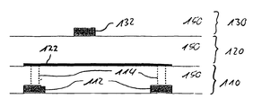
- FIG. 1 a is an exemplary inventive thin-film resistor layer as an additional intermediate plane, wherein contacting of the thin-film resistor layer is made by an underlying metal plane or polysilicon plane;
- FIG. 1 b is an exemplary inventive thin-film resistor layer as an additional intermediate layer, wherein contacting of the thin-film resistor layer is made by an overlying metal plane;
- FIG. 2 is an exemplary inventive thin-film resistor layer directly integrated into a corresponding metal plane
- FIG. 3 is an exemplary inventive thin-film resistor layer directly integrated into a corresponding metal plane, wherein conductive traces of the metal plane are deposited on the thin-film resistor layer and the metal is locally removed from the resistor layer for forming the resistor;
- FIG. 4 is a possible schematic design of wiring planes of a standard CMOS device, or process.
- the method for manufacturing, or the resulting device are each based on the previously described Ti/TiN layer order with suitable annealing, so as to realize the desired advantageous TCR values.
- the embodiments for the thin-film resistors of Ti/TiN layers set forth in the following show the diversity at different locations in which these Ti/TiN layers may be integrated in standard CMOS processes, or devices, however, they do not limit the invention to these embodiments.
- FIG 1 a shows an embodiment of an inventive thin-film resistor, or an inventive thin-film resistor layer, 122 in an exemplary CMOS device with three sheets, a first sheet 110 with a normal or common metal or polysilicon plane 112 , or conductive traces of normal metal or polysilicon, a second sheet 120 with the thin-film resistor 122 , and a third sheet 130 with a normal metal plane 132 , or conductive traces of normal metal.
- the sheets 110 , 120 , 130 further comprise an isolator 150 , e.g. of silicon oxide.
- the resistor layer has been introduced, as the second sheet 120 , as an additional intermediate plane, wherein contacting 114 of the thin-film resistor 122 is made by the underlying metal or polysilicon plane 112 .
- Typical materials for the contacting 114 include tungsten, for example.
- FIG. 1 b shows a further embodiment of an inventive thin-film resistor 122 , or an inventive thin-film resistor layer, wherein the thin-film resistor is inserted as an additional intermediate plane in an exemplary CMOS device with three sheets, with a first sheet 160 comprising a normal metal or polysilicon plane 162 , a second sheet 170 comprising the thin-film resistor 122 , and a third sheet 180 comprising a normal metal plane 182 , or conductive traces of normal metal.
- the conductive traces of normal metal, or polysilicon, and the thin-film resistor are separated by an isolator 150 .
- the thin-film resistor 122 is inserted as an additional intermediate plane, however, the contacting 172 is made via the overlying metal plane 182 .
- an isolating material typically silicon oxide
- Connecting the resistor layer is made by the underlying metal trace 112 , see FIG. 1 a , or the overlying metal trace 182 , see FIG. 1 b , for example.
- the contacting 114 may also be made via the polysilicon 112 , see FIG. 1 a , if necessitated.
- the TCR of the resistor layer 122 may be additionally decreased by suitable annealing. If this is permitted by the metallization layers, which may already be present, or if the resistor layer is annealed before depositing the first metallization layer, this annealing may be made at approximately 700° C. in nitrogen. If this high temperature is not compatible with the process, see aluminum metallization, it may be replaced with longer annealing at a lower temperature, if necessitated, as has been previously already explained.
- FIG. 2 shows an exemplary CMOS device with a further embodiment of an inventive thin-film resistor 122 , wherein the thin-film resistor 122 is directly integrated into a corresponding metal plane.
- FIG. 2 shows two sheets, a first sheet 210 with the thin-film resistor 122 and a normal metal plane 214 , and a second sheet 220 with further metal planes 224 , if necessitated.
- the sheets 210 and 220 further comprise an isolator 150 .
- the deposition of the resistor layer, its patterning and its annealing, if necessitated, are made directly before depositing one of the normal metallization layers 214 , which comprise aluminum as a material, for example.
- the metallization layer 214 is deposited and patterned.
- the metallization layer 214 is afterwards selectively etched to the Ti/TiN resistor layer 122 , so that the resistor is realized by a structure as depicted in FIG. 2 .
- the thin-film resistor 122 is contacted at the edge 122 R by the metallization layer 214 .
- the metallization layer 214 is selectively removed, so that only the resistor layer 122 remains there.
- the TCR of the resistor layer 122 may here also be optimized by suitable annealing.
- FIG. 3 shows a further exemplary CMOS device with a further embodiment of an inventive thin-film resistor 122 directly integrated into the corresponding metal plane.
- FIG. 3 shows a first sheet 310 with the thin-film resistor 122 and a normal metal plane 314 , and a second sheet 320 with further metal planes 324 , if necessitated.
- the sheets 310 and 320 further comprise an isolator 150 .
- deposition of the metallization layer 314 is made.
- This metallization layer 214 is then patterned together with the underlying resistor layer 122 .
- the metallization layer 314 is selectively removed in the resistor region 122 b .
- the resistor layer 122 in this metallization plane 310 remains under all metal traces 314 , unlike the variant shown in FIG. 2 .
- a Ti/TiN barrier layer which is already present in the process, may be used directly as a resistor layer if it has suitable layer thicknesses, which minimizes the additional expense needed for integrating the resistor 122 .
- an inventive thin-film resistor may comprise more than one Ti or TiN layer.
- Devices in which one or a plurality of inventive thin-film resistors are employed, are not limited to the numbers of layers, or sheets, shown in FIGS. 1 a , 1 b , 2 or 3 .
- devices comprising one or a plurality of inventive thin-film resistors are not limited to polysilicon or aluminum, for example, as conductive materials, but may comprise any conductive materials.
- corresponding devices may comprise different isolators or isolator materials in the individual sheets, or materials other than silicon oxide.
- inventive thin-film resistor or the method for manufacturing a thin-film resistor, are not limited to CMOS devices or processes only, but may also be applied in other technologies.
- Ti and TiN as volume crystals, comprise TCR values of several 1000 ppm/° C., which renders them unsuitable for highly precise applications.
- the material properties may be significantly modified, and, in particular, the temperature coefficient of resistance TCR may be significantly decreased.
- An additional possibility of modification results from a suitable temperature treatment, or annealing, of the layers, so that TCR values of almost zero, and, thus, temperature-independent resistors, or highly precise resistors, for integrated circuits with most demanding requirements may be provided for the inventive Ti/TiN thin-film resistors.
- Ti/TiN thin-film resistor lies in the fact that this material system is already used in most processes, and, thus, no additional investments in assemblies are needed and no contaminations come into the devices' range.
- microelectronical circuits integrated sensors and discrete, highly precise thin-film resistors, or fabrication processes employed in their manufacture, are fields of application for the invention described.
Abstract
Description
Claims (6)
Applications Claiming Priority (1)
| Application Number | Priority Date | Filing Date | Title |
|---|---|---|---|
| PCT/EP2005/013229 WO2007065460A1 (en) | 2005-12-09 | 2005-12-09 | Thin-film resistor having a layer structure and method for producing a thin-film resistor having a layer structure |
Publications (2)
| Publication Number | Publication Date |
|---|---|
| US20090206982A1 US20090206982A1 (en) | 2009-08-20 |
| US8026788B2 true US8026788B2 (en) | 2011-09-27 |
Family
ID=36693127
Family Applications (1)
| Application Number | Title | Priority Date | Filing Date |
|---|---|---|---|
| US12/095,756 Expired - Fee Related US8026788B2 (en) | 2005-12-09 | 2005-12-09 | Thin-film resistor with a layer structure and method for manufacturing a thin-film resistor with a layer structure |
Country Status (3)
| Country | Link |
|---|---|
| US (1) | US8026788B2 (en) |
| DE (1) | DE112005003768A5 (en) |
| WO (1) | WO2007065460A1 (en) |
Cited By (1)
| Publication number | Priority date | Publication date | Assignee | Title |
|---|---|---|---|---|
| US20160069758A1 (en) * | 2014-09-05 | 2016-03-10 | Piezocryst Advanced Sensorics Gmbh | Sensor element |
Families Citing this family (1)
| Publication number | Priority date | Publication date | Assignee | Title |
|---|---|---|---|---|
| JP5601566B2 (en) * | 2010-01-28 | 2014-10-08 | ルネサスエレクトロニクス株式会社 | Semiconductor device and manufacturing method thereof |
Citations (7)
| Publication number | Priority date | Publication date | Assignee | Title |
|---|---|---|---|---|
| US5723382A (en) * | 1992-06-12 | 1998-03-03 | Sandhu; Gurtej S. | Method of making a low-resistance contact to silicon having a titanium silicide interface, an amorphous titanium nitride barrier layer and a conductive plug |
| US6017789A (en) * | 1995-05-19 | 2000-01-25 | Micron Technology, Inc. | Method of forming a Ta2 O5 dielectric layer with amorphous diffusion barrier layer and method of forming a capacitor having a b. Ta.su2 O5 dielectric layer with amorphous diffusion barrier layer |
| US6028359A (en) * | 1997-03-12 | 2000-02-22 | Lucent Technologies Inc. | Integrated circuit having amorphous silicide layer in contacts and vias and method of manufacture therefor |
| US20010019301A1 (en) | 1998-06-12 | 2001-09-06 | Akinobu Shibuya | Thin-film resistor, wiring substrate, and method for manufacturing the same |
| US6313027B1 (en) * | 1995-08-07 | 2001-11-06 | Applied Materials, Inc. | Method for low thermal budget metal filling and planarization of contacts vias and trenches |
| US6607962B2 (en) * | 2001-08-09 | 2003-08-19 | Maxim Integrated Products, Inc. | Globally planarized backend compatible thin film resistor contact/interconnect process |
| US20050122207A1 (en) | 2003-12-04 | 2005-06-09 | Brian Vialpando | Thin film resistor structure and method of fabricating a thin film resistor structure |
-
2005
- 2005-12-09 DE DE112005003768T patent/DE112005003768A5/en not_active Ceased
- 2005-12-09 WO PCT/EP2005/013229 patent/WO2007065460A1/en active Application Filing
- 2005-12-09 US US12/095,756 patent/US8026788B2/en not_active Expired - Fee Related
Patent Citations (7)
| Publication number | Priority date | Publication date | Assignee | Title |
|---|---|---|---|---|
| US5723382A (en) * | 1992-06-12 | 1998-03-03 | Sandhu; Gurtej S. | Method of making a low-resistance contact to silicon having a titanium silicide interface, an amorphous titanium nitride barrier layer and a conductive plug |
| US6017789A (en) * | 1995-05-19 | 2000-01-25 | Micron Technology, Inc. | Method of forming a Ta2 O5 dielectric layer with amorphous diffusion barrier layer and method of forming a capacitor having a b. Ta.su2 O5 dielectric layer with amorphous diffusion barrier layer |
| US6313027B1 (en) * | 1995-08-07 | 2001-11-06 | Applied Materials, Inc. | Method for low thermal budget metal filling and planarization of contacts vias and trenches |
| US6028359A (en) * | 1997-03-12 | 2000-02-22 | Lucent Technologies Inc. | Integrated circuit having amorphous silicide layer in contacts and vias and method of manufacture therefor |
| US20010019301A1 (en) | 1998-06-12 | 2001-09-06 | Akinobu Shibuya | Thin-film resistor, wiring substrate, and method for manufacturing the same |
| US6607962B2 (en) * | 2001-08-09 | 2003-08-19 | Maxim Integrated Products, Inc. | Globally planarized backend compatible thin film resistor contact/interconnect process |
| US20050122207A1 (en) | 2003-12-04 | 2005-06-09 | Brian Vialpando | Thin film resistor structure and method of fabricating a thin film resistor structure |
Non-Patent Citations (2)
| Title |
|---|
| Official communication issued in counterpart International Application No. PCT/EP2005/013229, mailed on Oct. 8, 2006. |
| Wang et al.: "The Effect of Thermal Treatment on the Electrical Properties of Titanium Nitride Thiin Films by Filtered ARC Plasma Method," Ceramics International; vol. 30; No. 7; pp. 1921-1924; May 2004. |
Cited By (2)
| Publication number | Priority date | Publication date | Assignee | Title |
|---|---|---|---|---|
| US20160069758A1 (en) * | 2014-09-05 | 2016-03-10 | Piezocryst Advanced Sensorics Gmbh | Sensor element |
| US9618406B2 (en) * | 2014-09-05 | 2017-04-11 | Piezocryst Advanced Sensories Gmbh | Sensor element |
Also Published As
| Publication number | Publication date |
|---|---|
| DE112005003768A5 (en) | 2009-02-19 |
| US20090206982A1 (en) | 2009-08-20 |
| WO2007065460A1 (en) | 2007-06-14 |
Similar Documents
| Publication | Publication Date | Title |
|---|---|---|
| US7314786B1 (en) | Metal resistor, resistor material and method | |
| US7981761B2 (en) | Method of manufacturing semiconductor device having MIM capacitor | |
| US20090236689A1 (en) | Integrated passive device and method with low cost substrate | |
| CN101632174B (en) | Encapsulated metal resistor | |
| EP3391408B1 (en) | Oxidation resistant barrier metal for semiconductor devices and corresponding process | |
| US7669313B2 (en) | Method for fabricating a thin film resistor semiconductor structure | |
| WO2019245660A1 (en) | Semiconductor device with anti-deflection layers | |
| US9269579B2 (en) | Method for manufacturing silicon carbide semiconductor device | |
| US20050158910A1 (en) | Protective layer for use in packaging a semiconductor die and method for forming same | |
| US8026788B2 (en) | Thin-film resistor with a layer structure and method for manufacturing a thin-film resistor with a layer structure | |
| US6621404B1 (en) | Low temperature coefficient resistor | |
| CN109216320B (en) | Semiconductor device with a plurality of semiconductor chips | |
| US7193500B2 (en) | Thin film resistors of different materials | |
| US20140264865A1 (en) | Semiconductor device and manufacturing method thereof | |
| US7214295B2 (en) | Method for tantalum pentoxide moisture barrier in film resistors | |
| US20050277281A1 (en) | Compliant interconnect and method of formation | |
| JP5983024B2 (en) | Semiconductor device manufacturing method and semiconductor device | |
| US20060237724A1 (en) | Thin film transistor and method of forming the same | |
| US10978414B2 (en) | Semiconductor device and method of manufacturing a semiconductor device | |
| US7276777B2 (en) | Thin film resistor and method of making the same | |
| US20230134596A1 (en) | Metal stack to improve stack thermal stability | |
| US6153452A (en) | Method of manufacturing semiconductor devices having improved polycide integrity through introduction of a silicon layer within the polycide structure | |
| JP2003045983A (en) | Semiconductor device and its manufacturing method | |
| KR101100768B1 (en) | Method for forming polyresistor of semiconductor device | |
| JPH0428233A (en) | Manufacture of semiconductor device |
Legal Events
| Date | Code | Title | Description |
|---|---|---|---|
| AS | Assignment |
Owner name: FRAUNHOFER-GESELLSCHAFT ZUR FOERDERUNG DER ANGEWAN Free format text: ASSIGNMENT OF ASSIGNORS INTEREST;ASSIGNORS:DEITERS, HEINZ;LINNENBERG, SUSANNE;NACHRODT, DIRK;AND OTHERS;REEL/FRAME:021761/0829;SIGNING DATES FROM 20081013 TO 20081027 Owner name: UNIVERSITAET DULSBURG-ESSEN, GERMANY Free format text: ASSIGNMENT OF ASSIGNORS INTEREST;ASSIGNORS:DEITERS, HEINZ;LINNENBERG, SUSANNE;NACHRODT, DIRK;AND OTHERS;REEL/FRAME:021761/0829;SIGNING DATES FROM 20081013 TO 20081027 Owner name: FRAUNHOFER-GESELLSCHAFT ZUR FOERDERUNG DER ANGEWAN Free format text: ASSIGNMENT OF ASSIGNORS INTEREST;ASSIGNORS:DEITERS, HEINZ;LINNENBERG, SUSANNE;NACHRODT, DIRK;AND OTHERS;SIGNING DATES FROM 20081013 TO 20081027;REEL/FRAME:021761/0829 Owner name: UNIVERSITAET DULSBURG-ESSEN, GERMANY Free format text: ASSIGNMENT OF ASSIGNORS INTEREST;ASSIGNORS:DEITERS, HEINZ;LINNENBERG, SUSANNE;NACHRODT, DIRK;AND OTHERS;SIGNING DATES FROM 20081013 TO 20081027;REEL/FRAME:021761/0829 |
|
| AS | Assignment |
Owner name: FRAUNHOFER-GESELLSCHAFT ZUR FOERDERUNG DER ANGEWAN Free format text: CORRECTIVE ASSIGNMENT TO CORRECT THE NAME OF THE SECOND ASSIGNEE TO;ASSIGNORS:DEITERS, HEINZ;LINNENBERG, SUSANNE;NACHRODT, DIRK;AND OTHERS;REEL/FRAME:021914/0328;SIGNING DATES FROM 20081013 TO 20081027 Owner name: UNIVERSITAET DUISBURG-ESSEN, GERMANY Free format text: CORRECTIVE ASSIGNMENT TO CORRECT THE NAME OF THE SECOND ASSIGNEE TO;ASSIGNORS:DEITERS, HEINZ;LINNENBERG, SUSANNE;NACHRODT, DIRK;AND OTHERS;REEL/FRAME:021914/0328;SIGNING DATES FROM 20081013 TO 20081027 Owner name: FRAUNHOFER-GESELLSCHAFT ZUR FOERDERUNG DER ANGEWAN Free format text: CORRECTIVE ASSIGNMENT TO CORRECT THE NAME OF THE SECOND ASSIGNEE TO: UNIVERSITAET DUISBURG-ESSEN FORSTHAUSWEG 2 47057 DUISBURG, GERMANY PREVIOUSLY RECORDED ON REEL 021761 FRAME 0829. ASSIGNOR(S) HEREBY CONFIRMS THE ENTIRE INTEREST;ASSIGNORS:DEITERS, HEINZ;LINNENBERG, SUSANNE;NACHRODT, DIRK;AND OTHERS;SIGNING DATES FROM 20081013 TO 20081027;REEL/FRAME:021914/0328 Owner name: UNIVERSITAET DUISBURG-ESSEN, GERMANY Free format text: CORRECTIVE ASSIGNMENT TO CORRECT THE NAME OF THE SECOND ASSIGNEE TO: UNIVERSITAET DUISBURG-ESSEN FORSTHAUSWEG 2 47057 DUISBURG, GERMANY PREVIOUSLY RECORDED ON REEL 021761 FRAME 0829. ASSIGNOR(S) HEREBY CONFIRMS THE ENTIRE INTEREST;ASSIGNORS:DEITERS, HEINZ;LINNENBERG, SUSANNE;NACHRODT, DIRK;AND OTHERS;SIGNING DATES FROM 20081013 TO 20081027;REEL/FRAME:021914/0328 |
|
| FEPP | Fee payment procedure |
Free format text: PAYOR NUMBER ASSIGNED (ORIGINAL EVENT CODE: ASPN); ENTITY STATUS OF PATENT OWNER: LARGE ENTITY |
|
| REMI | Maintenance fee reminder mailed | ||
| LAPS | Lapse for failure to pay maintenance fees | ||
| STCH | Information on status: patent discontinuation |
Free format text: PATENT EXPIRED DUE TO NONPAYMENT OF MAINTENANCE FEES UNDER 37 CFR 1.362 |
|
| FP | Lapsed due to failure to pay maintenance fee |
Effective date: 20150927 |