US8030783B2 - Integrated circuit package with open substrate - Google Patents
Integrated circuit package with open substrate Download PDFInfo
- Publication number
- US8030783B2 US8030783B2 US12/582,587 US58258709A US8030783B2 US 8030783 B2 US8030783 B2 US 8030783B2 US 58258709 A US58258709 A US 58258709A US 8030783 B2 US8030783 B2 US 8030783B2
- Authority
- US
- United States
- Prior art keywords
- terminals
- conductive layer
- vias
- package
- forming
- Prior art date
- Legal status (The legal status is an assumption and is not a legal conclusion. Google has not performed a legal analysis and makes no representation as to the accuracy of the status listed.)
- Active
Links
Images


Classifications
-
- H—ELECTRICITY
- H01—ELECTRIC ELEMENTS
- H01L—SEMICONDUCTOR DEVICES NOT COVERED BY CLASS H10
- H01L25/00—Assemblies consisting of a plurality of individual semiconductor or other solid state devices ; Multistep manufacturing processes thereof
- H01L25/03—Assemblies consisting of a plurality of individual semiconductor or other solid state devices ; Multistep manufacturing processes thereof all the devices being of a type provided for in the same subgroup of groups H01L27/00 - H01L33/00, or in a single subclass of H10K, H10N, e.g. assemblies of rectifier diodes
- H01L25/04—Assemblies consisting of a plurality of individual semiconductor or other solid state devices ; Multistep manufacturing processes thereof all the devices being of a type provided for in the same subgroup of groups H01L27/00 - H01L33/00, or in a single subclass of H10K, H10N, e.g. assemblies of rectifier diodes the devices not having separate containers
- H01L25/065—Assemblies consisting of a plurality of individual semiconductor or other solid state devices ; Multistep manufacturing processes thereof all the devices being of a type provided for in the same subgroup of groups H01L27/00 - H01L33/00, or in a single subclass of H10K, H10N, e.g. assemblies of rectifier diodes the devices not having separate containers the devices being of a type provided for in group H01L27/00
- H01L25/0657—Stacked arrangements of devices
-
- H—ELECTRICITY
- H01—ELECTRIC ELEMENTS
- H01L—SEMICONDUCTOR DEVICES NOT COVERED BY CLASS H10
- H01L21/00—Processes or apparatus adapted for the manufacture or treatment of semiconductor or solid state devices or of parts thereof
- H01L21/02—Manufacture or treatment of semiconductor devices or of parts thereof
- H01L21/04—Manufacture or treatment of semiconductor devices or of parts thereof the devices having at least one potential-jump barrier or surface barrier, e.g. PN junction, depletion layer or carrier concentration layer
- H01L21/48—Manufacture or treatment of parts, e.g. containers, prior to assembly of the devices, using processes not provided for in a single one of the subgroups H01L21/06 - H01L21/326
- H01L21/4814—Conductive parts
- H01L21/4846—Leads on or in insulating or insulated substrates, e.g. metallisation
- H01L21/4857—Multilayer substrates
-
- H—ELECTRICITY
- H01—ELECTRIC ELEMENTS
- H01L—SEMICONDUCTOR DEVICES NOT COVERED BY CLASS H10
- H01L23/00—Details of semiconductor or other solid state devices
- H01L23/12—Mountings, e.g. non-detachable insulating substrates
- H01L23/13—Mountings, e.g. non-detachable insulating substrates characterised by the shape
-
- H—ELECTRICITY
- H01—ELECTRIC ELEMENTS
- H01L—SEMICONDUCTOR DEVICES NOT COVERED BY CLASS H10
- H01L23/00—Details of semiconductor or other solid state devices
- H01L23/48—Arrangements for conducting electric current to or from the solid state body in operation, e.g. leads, terminal arrangements ; Selection of materials therefor
- H01L23/488—Arrangements for conducting electric current to or from the solid state body in operation, e.g. leads, terminal arrangements ; Selection of materials therefor consisting of soldered or bonded constructions
- H01L23/498—Leads, i.e. metallisations or lead-frames on insulating substrates, e.g. chip carriers
- H01L23/49811—Additional leads joined to the metallisation on the insulating substrate, e.g. pins, bumps, wires, flat leads
- H01L23/49816—Spherical bumps on the substrate for external connection, e.g. ball grid arrays [BGA]
-
- H—ELECTRICITY
- H01—ELECTRIC ELEMENTS
- H01L—SEMICONDUCTOR DEVICES NOT COVERED BY CLASS H10
- H01L24/00—Arrangements for connecting or disconnecting semiconductor or solid-state bodies; Methods or apparatus related thereto
- H01L24/01—Means for bonding being attached to, or being formed on, the surface to be connected, e.g. chip-to-package, die-attach, "first-level" interconnects; Manufacturing methods related thereto
- H01L24/26—Layer connectors, e.g. plate connectors, solder or adhesive layers; Manufacturing methods related thereto
- H01L24/31—Structure, shape, material or disposition of the layer connectors after the connecting process
- H01L24/32—Structure, shape, material or disposition of the layer connectors after the connecting process of an individual layer connector
-
- H—ELECTRICITY
- H01—ELECTRIC ELEMENTS
- H01L—SEMICONDUCTOR DEVICES NOT COVERED BY CLASS H10
- H01L25/00—Assemblies consisting of a plurality of individual semiconductor or other solid state devices ; Multistep manufacturing processes thereof
- H01L25/03—Assemblies consisting of a plurality of individual semiconductor or other solid state devices ; Multistep manufacturing processes thereof all the devices being of a type provided for in the same subgroup of groups H01L27/00 - H01L33/00, or in a single subclass of H10K, H10N, e.g. assemblies of rectifier diodes
- H01L25/10—Assemblies consisting of a plurality of individual semiconductor or other solid state devices ; Multistep manufacturing processes thereof all the devices being of a type provided for in the same subgroup of groups H01L27/00 - H01L33/00, or in a single subclass of H10K, H10N, e.g. assemblies of rectifier diodes the devices having separate containers
- H01L25/105—Assemblies consisting of a plurality of individual semiconductor or other solid state devices ; Multistep manufacturing processes thereof all the devices being of a type provided for in the same subgroup of groups H01L27/00 - H01L33/00, or in a single subclass of H10K, H10N, e.g. assemblies of rectifier diodes the devices having separate containers the devices being of a type provided for in group H01L27/00
-
- H—ELECTRICITY
- H01—ELECTRIC ELEMENTS
- H01L—SEMICONDUCTOR DEVICES NOT COVERED BY CLASS H10
- H01L2224/00—Indexing scheme for arrangements for connecting or disconnecting semiconductor or solid-state bodies and methods related thereto as covered by H01L24/00
- H01L2224/01—Means for bonding being attached to, or being formed on, the surface to be connected, e.g. chip-to-package, die-attach, "first-level" interconnects; Manufacturing methods related thereto
- H01L2224/26—Layer connectors, e.g. plate connectors, solder or adhesive layers; Manufacturing methods related thereto
- H01L2224/31—Structure, shape, material or disposition of the layer connectors after the connecting process
- H01L2224/32—Structure, shape, material or disposition of the layer connectors after the connecting process of an individual layer connector
- H01L2224/321—Disposition
- H01L2224/32151—Disposition the layer connector connecting between a semiconductor or solid-state body and an item not being a semiconductor or solid-state body, e.g. chip-to-substrate, chip-to-passive
- H01L2224/32221—Disposition the layer connector connecting between a semiconductor or solid-state body and an item not being a semiconductor or solid-state body, e.g. chip-to-substrate, chip-to-passive the body and the item being stacked
- H01L2224/32225—Disposition the layer connector connecting between a semiconductor or solid-state body and an item not being a semiconductor or solid-state body, e.g. chip-to-substrate, chip-to-passive the body and the item being stacked the item being non-metallic, e.g. insulating substrate with or without metallisation
-
- H—ELECTRICITY
- H01—ELECTRIC ELEMENTS
- H01L—SEMICONDUCTOR DEVICES NOT COVERED BY CLASS H10
- H01L2224/00—Indexing scheme for arrangements for connecting or disconnecting semiconductor or solid-state bodies and methods related thereto as covered by H01L24/00
- H01L2224/01—Means for bonding being attached to, or being formed on, the surface to be connected, e.g. chip-to-package, die-attach, "first-level" interconnects; Manufacturing methods related thereto
- H01L2224/42—Wire connectors; Manufacturing methods related thereto
- H01L2224/47—Structure, shape, material or disposition of the wire connectors after the connecting process
- H01L2224/48—Structure, shape, material or disposition of the wire connectors after the connecting process of an individual wire connector
- H01L2224/4805—Shape
- H01L2224/4809—Loop shape
- H01L2224/48091—Arched
-
- H—ELECTRICITY
- H01—ELECTRIC ELEMENTS
- H01L—SEMICONDUCTOR DEVICES NOT COVERED BY CLASS H10
- H01L2224/00—Indexing scheme for arrangements for connecting or disconnecting semiconductor or solid-state bodies and methods related thereto as covered by H01L24/00
- H01L2224/01—Means for bonding being attached to, or being formed on, the surface to be connected, e.g. chip-to-package, die-attach, "first-level" interconnects; Manufacturing methods related thereto
- H01L2224/42—Wire connectors; Manufacturing methods related thereto
- H01L2224/47—Structure, shape, material or disposition of the wire connectors after the connecting process
- H01L2224/48—Structure, shape, material or disposition of the wire connectors after the connecting process of an individual wire connector
- H01L2224/481—Disposition
- H01L2224/48151—Connecting between a semiconductor or solid-state body and an item not being a semiconductor or solid-state body, e.g. chip-to-substrate, chip-to-passive
- H01L2224/48221—Connecting between a semiconductor or solid-state body and an item not being a semiconductor or solid-state body, e.g. chip-to-substrate, chip-to-passive the body and the item being stacked
- H01L2224/48225—Connecting between a semiconductor or solid-state body and an item not being a semiconductor or solid-state body, e.g. chip-to-substrate, chip-to-passive the body and the item being stacked the item being non-metallic, e.g. insulating substrate with or without metallisation
- H01L2224/48227—Connecting between a semiconductor or solid-state body and an item not being a semiconductor or solid-state body, e.g. chip-to-substrate, chip-to-passive the body and the item being stacked the item being non-metallic, e.g. insulating substrate with or without metallisation connecting the wire to a bond pad of the item
-
- H—ELECTRICITY
- H01—ELECTRIC ELEMENTS
- H01L—SEMICONDUCTOR DEVICES NOT COVERED BY CLASS H10
- H01L2224/00—Indexing scheme for arrangements for connecting or disconnecting semiconductor or solid-state bodies and methods related thereto as covered by H01L24/00
- H01L2224/01—Means for bonding being attached to, or being formed on, the surface to be connected, e.g. chip-to-package, die-attach, "first-level" interconnects; Manufacturing methods related thereto
- H01L2224/42—Wire connectors; Manufacturing methods related thereto
- H01L2224/47—Structure, shape, material or disposition of the wire connectors after the connecting process
- H01L2224/48—Structure, shape, material or disposition of the wire connectors after the connecting process of an individual wire connector
- H01L2224/481—Disposition
- H01L2224/48151—Connecting between a semiconductor or solid-state body and an item not being a semiconductor or solid-state body, e.g. chip-to-substrate, chip-to-passive
- H01L2224/48221—Connecting between a semiconductor or solid-state body and an item not being a semiconductor or solid-state body, e.g. chip-to-substrate, chip-to-passive the body and the item being stacked
- H01L2224/48225—Connecting between a semiconductor or solid-state body and an item not being a semiconductor or solid-state body, e.g. chip-to-substrate, chip-to-passive the body and the item being stacked the item being non-metallic, e.g. insulating substrate with or without metallisation
- H01L2224/48237—Connecting between a semiconductor or solid-state body and an item not being a semiconductor or solid-state body, e.g. chip-to-substrate, chip-to-passive the body and the item being stacked the item being non-metallic, e.g. insulating substrate with or without metallisation connecting the wire to a die pad of the item
-
- H—ELECTRICITY
- H01—ELECTRIC ELEMENTS
- H01L—SEMICONDUCTOR DEVICES NOT COVERED BY CLASS H10
- H01L2224/00—Indexing scheme for arrangements for connecting or disconnecting semiconductor or solid-state bodies and methods related thereto as covered by H01L24/00
- H01L2224/73—Means for bonding being of different types provided for in two or more of groups H01L2224/10, H01L2224/18, H01L2224/26, H01L2224/34, H01L2224/42, H01L2224/50, H01L2224/63, H01L2224/71
- H01L2224/732—Location after the connecting process
- H01L2224/73251—Location after the connecting process on different surfaces
- H01L2224/73265—Layer and wire connectors
-
- H—ELECTRICITY
- H01—ELECTRIC ELEMENTS
- H01L—SEMICONDUCTOR DEVICES NOT COVERED BY CLASS H10
- H01L2225/00—Details relating to assemblies covered by the group H01L25/00 but not provided for in its subgroups
- H01L2225/03—All the devices being of a type provided for in the same subgroup of groups H01L27/00 - H01L33/648 and H10K99/00
- H01L2225/04—All the devices being of a type provided for in the same subgroup of groups H01L27/00 - H01L33/648 and H10K99/00 the devices not having separate containers
- H01L2225/065—All the devices being of a type provided for in the same subgroup of groups H01L27/00 - H01L33/648 and H10K99/00 the devices not having separate containers the devices being of a type provided for in group H01L27/00
- H01L2225/06503—Stacked arrangements of devices
- H01L2225/0651—Wire or wire-like electrical connections from device to substrate
-
- H—ELECTRICITY
- H01—ELECTRIC ELEMENTS
- H01L—SEMICONDUCTOR DEVICES NOT COVERED BY CLASS H10
- H01L2225/00—Details relating to assemblies covered by the group H01L25/00 but not provided for in its subgroups
- H01L2225/03—All the devices being of a type provided for in the same subgroup of groups H01L27/00 - H01L33/648 and H10K99/00
- H01L2225/04—All the devices being of a type provided for in the same subgroup of groups H01L27/00 - H01L33/648 and H10K99/00 the devices not having separate containers
- H01L2225/065—All the devices being of a type provided for in the same subgroup of groups H01L27/00 - H01L33/648 and H10K99/00 the devices not having separate containers the devices being of a type provided for in group H01L27/00
- H01L2225/06503—Stacked arrangements of devices
- H01L2225/06541—Conductive via connections through the device, e.g. vertical interconnects, through silicon via [TSV]
-
- H—ELECTRICITY
- H01—ELECTRIC ELEMENTS
- H01L—SEMICONDUCTOR DEVICES NOT COVERED BY CLASS H10
- H01L2225/00—Details relating to assemblies covered by the group H01L25/00 but not provided for in its subgroups
- H01L2225/03—All the devices being of a type provided for in the same subgroup of groups H01L27/00 - H01L33/648 and H10K99/00
- H01L2225/04—All the devices being of a type provided for in the same subgroup of groups H01L27/00 - H01L33/648 and H10K99/00 the devices not having separate containers
- H01L2225/065—All the devices being of a type provided for in the same subgroup of groups H01L27/00 - H01L33/648 and H10K99/00 the devices not having separate containers the devices being of a type provided for in group H01L27/00
- H01L2225/06503—Stacked arrangements of devices
- H01L2225/06555—Geometry of the stack, e.g. form of the devices, geometry to facilitate stacking
-
- H—ELECTRICITY
- H01—ELECTRIC ELEMENTS
- H01L—SEMICONDUCTOR DEVICES NOT COVERED BY CLASS H10
- H01L2225/00—Details relating to assemblies covered by the group H01L25/00 but not provided for in its subgroups
- H01L2225/03—All the devices being of a type provided for in the same subgroup of groups H01L27/00 - H01L33/648 and H10K99/00
- H01L2225/04—All the devices being of a type provided for in the same subgroup of groups H01L27/00 - H01L33/648 and H10K99/00 the devices not having separate containers
- H01L2225/065—All the devices being of a type provided for in the same subgroup of groups H01L27/00 - H01L33/648 and H10K99/00 the devices not having separate containers the devices being of a type provided for in group H01L27/00
- H01L2225/06503—Stacked arrangements of devices
- H01L2225/06572—Auxiliary carrier between devices, the carrier having an electrical connection structure
-
- H—ELECTRICITY
- H01—ELECTRIC ELEMENTS
- H01L—SEMICONDUCTOR DEVICES NOT COVERED BY CLASS H10
- H01L2225/00—Details relating to assemblies covered by the group H01L25/00 but not provided for in its subgroups
- H01L2225/03—All the devices being of a type provided for in the same subgroup of groups H01L27/00 - H01L33/648 and H10K99/00
- H01L2225/04—All the devices being of a type provided for in the same subgroup of groups H01L27/00 - H01L33/648 and H10K99/00 the devices not having separate containers
- H01L2225/065—All the devices being of a type provided for in the same subgroup of groups H01L27/00 - H01L33/648 and H10K99/00 the devices not having separate containers the devices being of a type provided for in group H01L27/00
- H01L2225/06503—Stacked arrangements of devices
- H01L2225/06582—Housing for the assembly, e.g. chip scale package [CSP]
- H01L2225/06586—Housing with external bump or bump-like connectors
-
- H—ELECTRICITY
- H01—ELECTRIC ELEMENTS
- H01L—SEMICONDUCTOR DEVICES NOT COVERED BY CLASS H10
- H01L2225/00—Details relating to assemblies covered by the group H01L25/00 but not provided for in its subgroups
- H01L2225/03—All the devices being of a type provided for in the same subgroup of groups H01L27/00 - H01L33/648 and H10K99/00
- H01L2225/10—All the devices being of a type provided for in the same subgroup of groups H01L27/00 - H01L33/648 and H10K99/00 the devices having separate containers
- H01L2225/1005—All the devices being of a type provided for in the same subgroup of groups H01L27/00 - H01L33/648 and H10K99/00 the devices having separate containers the devices being of a type provided for in group H01L27/00
- H01L2225/1011—All the devices being of a type provided for in the same subgroup of groups H01L27/00 - H01L33/648 and H10K99/00 the devices having separate containers the devices being of a type provided for in group H01L27/00 the containers being in a stacked arrangement
- H01L2225/1047—Details of electrical connections between containers
- H01L2225/1058—Bump or bump-like electrical connections, e.g. balls, pillars, posts
-
- H—ELECTRICITY
- H01—ELECTRIC ELEMENTS
- H01L—SEMICONDUCTOR DEVICES NOT COVERED BY CLASS H10
- H01L24/00—Arrangements for connecting or disconnecting semiconductor or solid-state bodies; Methods or apparatus related thereto
- H01L24/01—Means for bonding being attached to, or being formed on, the surface to be connected, e.g. chip-to-package, die-attach, "first-level" interconnects; Manufacturing methods related thereto
- H01L24/42—Wire connectors; Manufacturing methods related thereto
- H01L24/47—Structure, shape, material or disposition of the wire connectors after the connecting process
- H01L24/48—Structure, shape, material or disposition of the wire connectors after the connecting process of an individual wire connector
-
- H—ELECTRICITY
- H01—ELECTRIC ELEMENTS
- H01L—SEMICONDUCTOR DEVICES NOT COVERED BY CLASS H10
- H01L24/00—Arrangements for connecting or disconnecting semiconductor or solid-state bodies; Methods or apparatus related thereto
- H01L24/73—Means for bonding being of different types provided for in two or more of groups H01L24/10, H01L24/18, H01L24/26, H01L24/34, H01L24/42, H01L24/50, H01L24/63, H01L24/71
-
- H—ELECTRICITY
- H01—ELECTRIC ELEMENTS
- H01L—SEMICONDUCTOR DEVICES NOT COVERED BY CLASS H10
- H01L2924/00—Indexing scheme for arrangements or methods for connecting or disconnecting semiconductor or solid-state bodies as covered by H01L24/00
- H01L2924/0001—Technical content checked by a classifier
- H01L2924/00014—Technical content checked by a classifier the subject-matter covered by the group, the symbol of which is combined with the symbol of this group, being disclosed without further technical details
-
- H—ELECTRICITY
- H01—ELECTRIC ELEMENTS
- H01L—SEMICONDUCTOR DEVICES NOT COVERED BY CLASS H10
- H01L2924/00—Indexing scheme for arrangements or methods for connecting or disconnecting semiconductor or solid-state bodies as covered by H01L24/00
- H01L2924/01—Chemical elements
- H01L2924/01013—Aluminum [Al]
-
- H—ELECTRICITY
- H01—ELECTRIC ELEMENTS
- H01L—SEMICONDUCTOR DEVICES NOT COVERED BY CLASS H10
- H01L2924/00—Indexing scheme for arrangements or methods for connecting or disconnecting semiconductor or solid-state bodies as covered by H01L24/00
- H01L2924/01—Chemical elements
- H01L2924/01027—Cobalt [Co]
-
- H—ELECTRICITY
- H01—ELECTRIC ELEMENTS
- H01L—SEMICONDUCTOR DEVICES NOT COVERED BY CLASS H10
- H01L2924/00—Indexing scheme for arrangements or methods for connecting or disconnecting semiconductor or solid-state bodies as covered by H01L24/00
- H01L2924/01—Chemical elements
- H01L2924/01029—Copper [Cu]
-
- H—ELECTRICITY
- H01—ELECTRIC ELEMENTS
- H01L—SEMICONDUCTOR DEVICES NOT COVERED BY CLASS H10
- H01L2924/00—Indexing scheme for arrangements or methods for connecting or disconnecting semiconductor or solid-state bodies as covered by H01L24/00
- H01L2924/01—Chemical elements
- H01L2924/01033—Arsenic [As]
-
- H—ELECTRICITY
- H01—ELECTRIC ELEMENTS
- H01L—SEMICONDUCTOR DEVICES NOT COVERED BY CLASS H10
- H01L2924/00—Indexing scheme for arrangements or methods for connecting or disconnecting semiconductor or solid-state bodies as covered by H01L24/00
- H01L2924/01—Chemical elements
- H01L2924/01076—Osmium [Os]
-
- H—ELECTRICITY
- H01—ELECTRIC ELEMENTS
- H01L—SEMICONDUCTOR DEVICES NOT COVERED BY CLASS H10
- H01L2924/00—Indexing scheme for arrangements or methods for connecting or disconnecting semiconductor or solid-state bodies as covered by H01L24/00
- H01L2924/01—Chemical elements
- H01L2924/01078—Platinum [Pt]
-
- H—ELECTRICITY
- H01—ELECTRIC ELEMENTS
- H01L—SEMICONDUCTOR DEVICES NOT COVERED BY CLASS H10
- H01L2924/00—Indexing scheme for arrangements or methods for connecting or disconnecting semiconductor or solid-state bodies as covered by H01L24/00
- H01L2924/01—Chemical elements
- H01L2924/01079—Gold [Au]
-
- H—ELECTRICITY
- H01—ELECTRIC ELEMENTS
- H01L—SEMICONDUCTOR DEVICES NOT COVERED BY CLASS H10
- H01L2924/00—Indexing scheme for arrangements or methods for connecting or disconnecting semiconductor or solid-state bodies as covered by H01L24/00
- H01L2924/01—Chemical elements
- H01L2924/01082—Lead [Pb]
-
- H—ELECTRICITY
- H01—ELECTRIC ELEMENTS
- H01L—SEMICONDUCTOR DEVICES NOT COVERED BY CLASS H10
- H01L2924/00—Indexing scheme for arrangements or methods for connecting or disconnecting semiconductor or solid-state bodies as covered by H01L24/00
- H01L2924/013—Alloys
- H01L2924/0132—Binary Alloys
-
- H—ELECTRICITY
- H01—ELECTRIC ELEMENTS
- H01L—SEMICONDUCTOR DEVICES NOT COVERED BY CLASS H10
- H01L2924/00—Indexing scheme for arrangements or methods for connecting or disconnecting semiconductor or solid-state bodies as covered by H01L24/00
- H01L2924/013—Alloys
- H01L2924/014—Solder alloys
-
- H—ELECTRICITY
- H01—ELECTRIC ELEMENTS
- H01L—SEMICONDUCTOR DEVICES NOT COVERED BY CLASS H10
- H01L2924/00—Indexing scheme for arrangements or methods for connecting or disconnecting semiconductor or solid-state bodies as covered by H01L24/00
- H01L2924/10—Details of semiconductor or other solid state devices to be connected
- H01L2924/11—Device type
- H01L2924/12—Passive devices, e.g. 2 terminal devices
- H01L2924/1204—Optical Diode
- H01L2924/12042—LASER
-
- H—ELECTRICITY
- H01—ELECTRIC ELEMENTS
- H01L—SEMICONDUCTOR DEVICES NOT COVERED BY CLASS H10
- H01L2924/00—Indexing scheme for arrangements or methods for connecting or disconnecting semiconductor or solid-state bodies as covered by H01L24/00
- H01L2924/10—Details of semiconductor or other solid state devices to be connected
- H01L2924/11—Device type
- H01L2924/14—Integrated circuits
-
- H—ELECTRICITY
- H01—ELECTRIC ELEMENTS
- H01L—SEMICONDUCTOR DEVICES NOT COVERED BY CLASS H10
- H01L2924/00—Indexing scheme for arrangements or methods for connecting or disconnecting semiconductor or solid-state bodies as covered by H01L24/00
- H01L2924/15—Details of package parts other than the semiconductor or other solid state devices to be connected
- H01L2924/151—Die mounting substrate
- H01L2924/1515—Shape
- H01L2924/15153—Shape the die mounting substrate comprising a recess for hosting the device
-
- H—ELECTRICITY
- H01—ELECTRIC ELEMENTS
- H01L—SEMICONDUCTOR DEVICES NOT COVERED BY CLASS H10
- H01L2924/00—Indexing scheme for arrangements or methods for connecting or disconnecting semiconductor or solid-state bodies as covered by H01L24/00
- H01L2924/15—Details of package parts other than the semiconductor or other solid state devices to be connected
- H01L2924/151—Die mounting substrate
- H01L2924/15165—Monolayer substrate
-
- H—ELECTRICITY
- H01—ELECTRIC ELEMENTS
- H01L—SEMICONDUCTOR DEVICES NOT COVERED BY CLASS H10
- H01L2924/00—Indexing scheme for arrangements or methods for connecting or disconnecting semiconductor or solid-state bodies as covered by H01L24/00
- H01L2924/15—Details of package parts other than the semiconductor or other solid state devices to be connected
- H01L2924/151—Die mounting substrate
- H01L2924/1517—Multilayer substrate
-
- H—ELECTRICITY
- H01—ELECTRIC ELEMENTS
- H01L—SEMICONDUCTOR DEVICES NOT COVERED BY CLASS H10
- H01L2924/00—Indexing scheme for arrangements or methods for connecting or disconnecting semiconductor or solid-state bodies as covered by H01L24/00
- H01L2924/15—Details of package parts other than the semiconductor or other solid state devices to be connected
- H01L2924/151—Die mounting substrate
- H01L2924/153—Connection portion
- H01L2924/1531—Connection portion the connection portion being formed only on the surface of the substrate opposite to the die mounting surface
- H01L2924/15311—Connection portion the connection portion being formed only on the surface of the substrate opposite to the die mounting surface being a ball array, e.g. BGA
-
- H—ELECTRICITY
- H01—ELECTRIC ELEMENTS
- H01L—SEMICONDUCTOR DEVICES NOT COVERED BY CLASS H10
- H01L2924/00—Indexing scheme for arrangements or methods for connecting or disconnecting semiconductor or solid-state bodies as covered by H01L24/00
- H01L2924/15—Details of package parts other than the semiconductor or other solid state devices to be connected
- H01L2924/151—Die mounting substrate
- H01L2924/153—Connection portion
- H01L2924/1532—Connection portion the connection portion being formed on the die mounting surface of the substrate
- H01L2924/1533—Connection portion the connection portion being formed on the die mounting surface of the substrate the connection portion being formed both on the die mounting surface of the substrate and outside the die mounting surface of the substrate
- H01L2924/15331—Connection portion the connection portion being formed on the die mounting surface of the substrate the connection portion being formed both on the die mounting surface of the substrate and outside the die mounting surface of the substrate being a ball array, e.g. BGA
-
- H—ELECTRICITY
- H01—ELECTRIC ELEMENTS
- H01L—SEMICONDUCTOR DEVICES NOT COVERED BY CLASS H10
- H01L2924/00—Indexing scheme for arrangements or methods for connecting or disconnecting semiconductor or solid-state bodies as covered by H01L24/00
- H01L2924/15—Details of package parts other than the semiconductor or other solid state devices to be connected
- H01L2924/181—Encapsulation
-
- H—ELECTRICITY
- H01—ELECTRIC ELEMENTS
- H01L—SEMICONDUCTOR DEVICES NOT COVERED BY CLASS H10
- H01L2924/00—Indexing scheme for arrangements or methods for connecting or disconnecting semiconductor or solid-state bodies as covered by H01L24/00
- H01L2924/30—Technical effects
- H01L2924/35—Mechanical effects
- H01L2924/351—Thermal stress
- H01L2924/3511—Warping
-
- Y—GENERAL TAGGING OF NEW TECHNOLOGICAL DEVELOPMENTS; GENERAL TAGGING OF CROSS-SECTIONAL TECHNOLOGIES SPANNING OVER SEVERAL SECTIONS OF THE IPC; TECHNICAL SUBJECTS COVERED BY FORMER USPC CROSS-REFERENCE ART COLLECTIONS [XRACs] AND DIGESTS
- Y10—TECHNICAL SUBJECTS COVERED BY FORMER USPC
- Y10S—TECHNICAL SUBJECTS COVERED BY FORMER USPC CROSS-REFERENCE ART COLLECTIONS [XRACs] AND DIGESTS
- Y10S438/00—Semiconductor device manufacturing: process
- Y10S438/928—Front and rear surface processing
Definitions
- the present invention relates generally to semiconductor packages, and more particularly to leadless and ball grid array chip scale packages.
- Semiconductor devices are constructed from a silicon (Si) or gallium-arsenide (Ga/As) wafer through a process that comprises a number of deposition, masking, diffusion, etching, and implanting steps. Usually, many individual devices are constructed on the same wafer. When the devices are separated into individual groups of units, each takes the form of an integrated circuit die.
- Si silicon
- Ga/As gallium-arsenide
- the dies are commonly mounted on a substrate that is surrounded by a number of lead fingers.
- Each die has bonding pads that are then individually connected in a wire bonding operation to the lead fingers and the assemblies are then packaged by individually encapsulating them in molded plastic, epoxy, or ceramic bodies.
- the lead fingers of the packages are then processed for attachment to a printed circuit board.
- quad flat no lead (QFN) package One type of package is the quad flat no lead (QFN) package.
- the QFN package has the die adhesively bonded to a lead paddle which, along with the lead fingers, is exposed.
- the QFN package has good electrical and thermal characteristics, however, to increase the number of input/outputs (I/O) for a given body size, it is necessary to reduce the width of the lead fingers and/or insert more rows of lead fingers. However, when the width of the lead fingers is decreased, handling problems are encountered during manufacturing.
- PLGA plastic land grid array
- a die is bonded to a paddle and the paddle is bonded to a substrate.
- the substrate has patterned metal on both sides and through vias connecting the patterned metal.
- LPI liquid photoimageable solder mask
- Adhesion between the LPI solder mask on large metal surfaces is poor, and the packages consistently have problems passing inspection, especially with regard to moisture resistance.
- solder mask registration and resolution cause problems because they affect bonding pad size.
- solder mask layer increases the thermal resistance from the chip to the printed circuit board resulting in inferior thermal dissipation compared to the QFN package.
- the PLGA package requires off-set vias requiring a connection between the via and the land.
- the present invention provides a method of manufacturing an integrated circuit package that includes: forming a substrate that includes: forming a core layer, forming vias in the core layer, and forming a conductive layer having a predetermined thickness on the core layer and having substantially twice the predetermined thickness in the vias; and forming connections between an integrated circuit die and the conductive layer.
- the present invention provides an integrated circuit package that includes: a substrate including a core layer having vias provided therein; a conductive layer having a predetermined thickness on the core layer and having substantially twice the predetermined thickness in the vias; an integrated circuit over the substrate; and connections between the integrated circuit die and the conductive layer.
- FIG. 1 is a cross-sectional side view of one embodiment of a thermally/electrically enhanced super thin die up chip scale package in accordance with the present invention.
- FIG. 2 is an isometric bottom side view of the structure of FIG. 1 including an encapsulant.
- FIG. 3 is an isometric topside view of the structure of FIG. 1 without an encapsulant.
- FIG. 4 is a cross-sectional side view of an embodiment of a thermally/electrically enhanced super thin die down chip scale package in accordance with the present invention.
- FIG. 5 is an isometric top side view of a first conductive layer of FIG. 4 .
- FIG. 6 is an isometric bottom side view of the structure of FIG. 4 including an encapsulant and solder balls.
- FIG. 7 is a bottom view of a chip scale package with rectangular-shaped dual rows of terminals.
- FIG. 8 is a view of a chip scale package with circular-shaped dual rows of terminals.
- FIG. 9 is a view of a package-to-package stack in accordance with an additional embodiment of the present invention.
- FIG. 10 is a view of a multi-package-to-package stack in accordance with a further embodiment of the present invention.
- FIG. 11 is an isometric top side view of the structure of FIG. 10 with an optional solder mask.
- FIG. 12 is an isometric topside view of the structure of FIG. 10 without a solder mask.
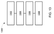
- FIG. 13 shows a method of manufacturing an integrated circuit package.
- the CSP 100 includes a core layer 102 having a first conductive layer 104 and a second conductive layer 106 on opposite sides.
- the core layer 102 can be a non-conductive material such as such as thin core glass (bismaleimide triazine (BT) resin), epoxy laminate, or polyimide and the first and second conductive layers 104 and 106 can be of conductive metals such as aluminum (Al), copper (Cu), and gold (Au).
- An integrated circuit die 108 is bonded with a die attach adhesive 110 to the second conductive layer 106 .
- the die attach adhesive 110 may be of thermally and/or electrically conductive or non-conductive material such as epoxy or glass. This increases the thermal dissipation capability of the present invention.
- the integrated circuit die 108 is connected by ground wires 112 and signal wires 114 to the second conductive layer 106 .
- the ground and signal wires 112 and 114 are of such conductive materials as aluminum, copper, or gold.
- horizontal as used herein is defined as a plane parallel to the conventional plane or surface of the integrated circuit die, regardless of its orientation.
- vertical refers to a direction perpendicular to the horizontal as just defined. Terms, such as “on”, “above”, “below”, “bottom”, “top”, “over”, and “under”, are defined with respect to the horizontal plane.
- processing includes deposition of material or photoresist, patterning, exposure, development, etching, cleaning, and/or removal of the material or photoresist as required in forming a described structure.
- the core layer 102 has a central opening 120 for containing the integrated circuit die 108 and a number of perimeter openings or vias 122 surrounding the central opening 120 .
- the central opening 120 and the perimeter vias 122 extend through the core layer 102 .
- the first conductive layer 104 is processed to form a ground or thermal pad 130 surrounded by terminals 132 .
- the ground or thermal pad 130 closes the central opening 120 in the core layer 102
- the terminals 132 close the perimeter vias 122 in the core layer 102 .
- the second conductive layer 106 is processed to form ground or thermal terminals 140 surrounded by a number of signal terminals 142 .
- the ground or thermal terminals 140 extend through the central opening 120 of the core layer 102 to be in contact with the ground or thermal pad 130 of the first conductive layer 104 .
- the ground or thermal terminals 140 further have an encircling ground ring 144 to which ground wires 112 are bonded.
- the signal wires 114 are bonded to the signal terminals 142 .
- the signal terminals 142 extend through the perimeter vias 122 in the core layer 102 to be in contact with the terminals 132 of the first conductive layer 104 . While the perimeter vias 122 and the central opening 120 extend through the core layer 102 , the signal terminals 142 and the ground or thermal terminal 140 effectively close off the openings to provide “blind” openings or “blind vias” so the openings effectively do not extend through the core layer 102 .
- no solder mask layer is required at the top and bottom layers, which results in better adhesion between the encapsulating material and the layers. This in turn means there is less moisture uptake. Further, because of the blind vias, there is no direct moisture pathway through to the integrated circuit die 108 .
- the integrated circuit die 108 is die up because of contact pads (not shown) on its top surface to which the ground wires 112 and the signal wires 114 are bonded.
- the CSP 100 further includes an encapsulant 150 , such as plastic or epoxy, encapsulating the second conductive layer 106 , the integrated circuit die 108 , the die attach adhesive 110 , the ground wires 112 , and the signal wires 114 .
- an encapsulant 150 such as plastic or epoxy, encapsulating the second conductive layer 106 , the integrated circuit die 108 , the die attach adhesive 110 , the ground wires 112 , and the signal wires 114 .
- FIG. 2 therein is shown an isometric bottom side view of the CSP 100 .
- the ground or thermal pad 130 and the terminals 132 are shown raised.
- terminals 132 which extend or protrude from the core layer 102 , improve surface mount yield and solder joint reliability. Further, solder formation is improved around the vertical sides of the terminals 132 .
- FIG. 3 therein is shown an isometric topside view of the CSP 100 without the encapsulant 150 .
- the integrated circuit die 108 is shown surrounded by the ground ring 144 and by the signal terminals 142 .
- the ground wires 112 may be bonded any place along the ground ring 144 thereby increasing the possibility of heat transfer as well as multiple ground paths.
- the CSP 400 includes a core layer 402 having a first conductive layer 404 and a second conductive layer 406 on opposite sides.
- the core layer 402 can be a non-conductive material such as such as thin core glass (bismaleimide triazine resin), epoxy laminate, or polyimide and the first and second conductive layers 404 and 406 can be of conductive metals such as aluminum, copper, or gold.
- An integrated circuit die 408 is bonded with a die attach adhesive 410 to the second conductive layer 406 .
- the die attach adhesive 410 may be of thermally and/or electrically conductive or non-conductive material such as epoxy or glass.
- the integrated circuit die 408 is connected by ground wires 412 and signal wires 414 to the second conductive layer 406 .
- the ground and signal wires 412 and 414 are of materials such as aluminum, copper, or gold.
- the core layer 402 has a central opening 420 for containing the integrated circuit die 408 and a number of perimeter openings or vias 422 surrounding the central opening 420 .
- the central opening 420 and the perimeter vias 422 extend through the core layer 402 .
- the first conductive layer 404 closes the central opening 420 and the perimeter vias 422 in the core layer 402 , and forms a ground or thermal pad.
- the second conductive layer 406 is processed to form ground or thermal terminals 440 and 442 with a number of signal terminals 444 in between.
- the ground or thermal terminals 440 extend through the central opening 420 of the core layer 402 to form a ground or thermal pad 446 in contact with the first conductive layer 404 . This means that no additional processes or material are required for a silicon substrate backside ground.
- the ground or thermal terminals 442 extend through the perimeter openings or vias 422 to form blind vias in contact with the first conductive layer 404 .
- the second conductive layer 406 can be of a predetermined thickness 407 , and when extending through the vias 422 , can fold on itself, so that the fold of the second conductive layer 406 has substantially twice the predetermined thickness 407 in the vias 422 . It will also be understood from this disclosure that, if the first conductive layer 404 is patterned, the ground or thermal terminals 442 can be used as signal terminals.
- the integrated circuit die 408 is die down because of contact pads on its top surface, which faces down, to which the ground wires 412 and the signal wires 414 are bonded.
- a solder mask 450 is formed on the second conductive layer 406 with a number of through openings 452 to the second conductive layer 406 .
- Solder balls 460 are formed in contact with the signal terminals 444 through the solder mask 450
- solder balls 462 are formed in contact with the ground terminals 462 through the solder mask 450 .
- the CSP 400 further includes an encapsulant 465 , such as plastic or epoxy, encapsulating the second conductive layer 406 , the integrated circuit die 408 , the die attach adhesive 410 , the ground wires 412 , and the signal wires 414 .
- an encapsulant 465 such as plastic or epoxy, encapsulating the second conductive layer 406 , the integrated circuit die 408 , the die attach adhesive 410 , the ground wires 412 , and the signal wires 414 .
- FIG. 5 therein is shown an isometric top side view of the first conductive substrate 404 as the ground or thermal pad.
- FIG. 6 therein is shown an isometric bottom side view of the CSP 400 showing the encapsulant 465 , the solder mask 450 , and the solder balls 460 and 462 .
- FIG. 7 therein is shown a bottom view of a CSP 700 having rectangular-shaped dual rows of terminals 702 .
- FIG. 8 therein is shown a CSP 800 having circular-shaped dual rows of terminals 802 .
- the package-to-package stack 900 by way of example and for ease of explanation includes a CSP package 100 ′ stacked on and surface mounted to a modified version of the CSP package 400 ′.
- the first conductive layer 404 is processed to form a central ground or thermal pad 902 surrounded by terminals 904 .
- the central ground or thermal pad 902 is separated by an insulator ring 906 from the terminals 904 .
- a solder paste 910 is used to bond the first conductive layer 104 of the CSP 100 ′ to the first conductive layer 404 of the CSP 400 ′.
- the multi-package-to-package stack 1000 by way of example and for ease of explanation includes a modified CSP packages 400 ′ on top of a modified CSP package 400 ′′.
- the first conductive layer 404 of the CSP package 400 ′′ is processed to form terminals 1002 , 1004 , and 1006 .
- the solder balls 460 and 462 of the CSP package 400 ′ are respectively ball-bonded to the terminals 1004 and 1006 of the CSP package 400 ′′.
- FIG. 11 therein is shown an isometric top side view of the multi-package-to-package stack 1000 in accordance with the present invention.
- the multi-package-to-package stack 1000 has an solder mask 1010 having openings through which the terminals 1004 and 1006 are accessed.
- FIG. 12 therein is shown an alternative isometric top side view of the multi-package-to-package stack 1000 .
- the multi-package-to-package stack 1000 is without a solder mask and shows a core layer 402 ′ and uses circular-shaped dual row of the solder pads 1002 ′, 1004 ′, and 1006 ′, which protrude outward for solder ball contact.
- the method 1300 includes: a block 1302 of forming a substrate by forming a core layer, forming a through opening and vias in the core layer, forming a first conductive layer on the core layer covering the through opening, and forming a second conductive layer on the core layer opposite the first conductive layer in the through opening and in the vias contacting the first conductive layer; a block 1304 of bonding an integrated circuit die to the second conductive layer and in the through opening; a block 1306 of forming connections between the integrated circuit die and the second conductive layer; and a block 1308 of encapsulating the integrated circuit die and the connections.
- thermal dissipation because of direct heat flow from the integrated circuit die to a printed circuit board or a lower integrated circuit package; e.g., low thermal resistance throughout.
- electrical performance with very short signal paths, direct wire bonding over the terminals by the lined vias in the pads, and extremely low electrical resistance where pure copper (Cu) and gold (Au) are used in bonding and in the terminals.
Abstract
Description
Claims (14)
Priority Applications (2)
| Application Number | Priority Date | Filing Date | Title |
|---|---|---|---|
| US12/582,587 US8030783B2 (en) | 2004-06-10 | 2009-10-20 | Integrated circuit package with open substrate |
| US13/247,890 US9034693B2 (en) | 2004-06-10 | 2011-09-28 | Integrated circuit package with open substrate and method of manufacturing thereof |
Applications Claiming Priority (3)
| Application Number | Priority Date | Filing Date | Title |
|---|---|---|---|
| US10/866,561 US7008820B2 (en) | 2004-06-10 | 2004-06-10 | Chip scale package with open substrate |
| US11/164,329 US7626277B2 (en) | 2004-06-10 | 2005-11-18 | Integrated circuit package with open substrate |
| US12/582,587 US8030783B2 (en) | 2004-06-10 | 2009-10-20 | Integrated circuit package with open substrate |
Related Parent Applications (1)
| Application Number | Title | Priority Date | Filing Date |
|---|---|---|---|
| US11/164,329 Continuation US7626277B2 (en) | 2004-06-10 | 2005-11-18 | Integrated circuit package with open substrate |
Related Child Applications (1)
| Application Number | Title | Priority Date | Filing Date |
|---|---|---|---|
| US13/247,890 Continuation US9034693B2 (en) | 2004-06-10 | 2011-09-28 | Integrated circuit package with open substrate and method of manufacturing thereof |
Publications (2)
| Publication Number | Publication Date |
|---|---|
| US20100038771A1 US20100038771A1 (en) | 2010-02-18 |
| US8030783B2 true US8030783B2 (en) | 2011-10-04 |
Family
ID=35461053
Family Applications (4)
| Application Number | Title | Priority Date | Filing Date |
|---|---|---|---|
| US10/866,561 Active 2024-06-17 US7008820B2 (en) | 2004-06-10 | 2004-06-10 | Chip scale package with open substrate |
| US11/164,329 Active 2025-03-07 US7626277B2 (en) | 2004-06-10 | 2005-11-18 | Integrated circuit package with open substrate |
| US12/582,587 Active US8030783B2 (en) | 2004-06-10 | 2009-10-20 | Integrated circuit package with open substrate |
| US13/247,890 Active 2024-10-22 US9034693B2 (en) | 2004-06-10 | 2011-09-28 | Integrated circuit package with open substrate and method of manufacturing thereof |
Family Applications Before (2)
| Application Number | Title | Priority Date | Filing Date |
|---|---|---|---|
| US10/866,561 Active 2024-06-17 US7008820B2 (en) | 2004-06-10 | 2004-06-10 | Chip scale package with open substrate |
| US11/164,329 Active 2025-03-07 US7626277B2 (en) | 2004-06-10 | 2005-11-18 | Integrated circuit package with open substrate |
Family Applications After (1)
| Application Number | Title | Priority Date | Filing Date |
|---|---|---|---|
| US13/247,890 Active 2024-10-22 US9034693B2 (en) | 2004-06-10 | 2011-09-28 | Integrated circuit package with open substrate and method of manufacturing thereof |
Country Status (2)
| Country | Link |
|---|---|
| US (4) | US7008820B2 (en) |
| SG (3) | SG136138A1 (en) |
Cited By (1)
| Publication number | Priority date | Publication date | Assignee | Title |
|---|---|---|---|---|
| US20120018886A1 (en) * | 2004-06-10 | 2012-01-26 | Il Kwon Shim | Integrated circuit package with open substrate and method of manufacturing thereof |
Families Citing this family (25)
| Publication number | Priority date | Publication date | Assignee | Title |
|---|---|---|---|---|
| TWI234860B (en) * | 2004-04-02 | 2005-06-21 | Advanced Semiconductor Eng | Chip package and process thereof |
| JP2006041438A (en) * | 2004-07-30 | 2006-02-09 | Shinko Electric Ind Co Ltd | Semiconductor chip built-in substrate, and its manufacturing method |
| US8125076B2 (en) * | 2004-11-12 | 2012-02-28 | Stats Chippac Ltd. | Semiconductor package system with substrate heat sink |
| TWI269359B (en) * | 2005-05-06 | 2006-12-21 | Harvatek Corp | Manufacturing method for two pieces substrate package structures of photoelectric chip with controlling chip |
| US7981702B2 (en) * | 2006-03-08 | 2011-07-19 | Stats Chippac Ltd. | Integrated circuit package in package system |
| US7838971B2 (en) * | 2006-07-11 | 2010-11-23 | Atmel Corporation | Method to provide substrate-ground coupling for semiconductor integrated circuit dice constructed from SOI and related materials in stacked-die packages |
| JP5186741B2 (en) * | 2006-08-18 | 2013-04-24 | 富士通セミコンダクター株式会社 | Circuit board and semiconductor device |
| US8148804B2 (en) * | 2008-01-15 | 2012-04-03 | Dai Nippon Printing Co., Ltd. | Wiring device for semiconductor device, composite wiring device for semiconductor device, and resin-sealed semiconductor device |
| US8492883B2 (en) * | 2008-03-14 | 2013-07-23 | Advanced Semiconductor Engineering, Inc. | Semiconductor package having a cavity structure |
| US7863732B2 (en) * | 2008-03-18 | 2011-01-04 | Stats Chippac Ltd. | Ball grid array package system |
| US8324723B2 (en) * | 2008-03-25 | 2012-12-04 | Bridge Semiconductor Corporation | Semiconductor chip assembly with bump/base heat spreader and dual-angle cavity in bump |
| US8129742B2 (en) * | 2008-03-25 | 2012-03-06 | Bridge Semiconductor Corporation | Semiconductor chip assembly with post/base heat spreader and plated through-hole |
| US8314438B2 (en) * | 2008-03-25 | 2012-11-20 | Bridge Semiconductor Corporation | Semiconductor chip assembly with bump/base heat spreader and cavity in bump |
| US20110042794A1 (en) * | 2008-05-19 | 2011-02-24 | Tung-Hsien Hsieh | Qfn semiconductor package and circuit board structure adapted for the same |
| US20100044850A1 (en) * | 2008-08-21 | 2010-02-25 | Advanced Semiconductor Engineering, Inc. | Advanced quad flat non-leaded package structure and manufacturing method thereof |
| US7871862B2 (en) * | 2008-09-08 | 2011-01-18 | Stats Chippac Ltd. | Ball grid array package stacking system |
| US8089145B1 (en) * | 2008-11-17 | 2012-01-03 | Amkor Technology, Inc. | Semiconductor device including increased capacity leadframe |
| US8124447B2 (en) | 2009-04-10 | 2012-02-28 | Advanced Semiconductor Engineering, Inc. | Manufacturing method of advanced quad flat non-leaded package |
| US8164199B2 (en) * | 2009-07-31 | 2012-04-24 | Alpha and Omega Semiconductor Incorporation | Multi-die package |
| US20110163430A1 (en) * | 2010-01-06 | 2011-07-07 | Advanced Semiconductor Engineering, Inc. | Leadframe Structure, Advanced Quad Flat No Lead Package Structure Using the Same, and Manufacturing Methods Thereof |
| CN103930987A (en) * | 2011-07-25 | 2014-07-16 | 兰克森法国公司 | Lead frameless hermetic circuit package |
| US9275877B2 (en) | 2011-09-20 | 2016-03-01 | Stats Chippac, Ltd. | Semiconductor device and method of forming semiconductor package using panel form carrier |
| CN103367351B (en) * | 2013-07-15 | 2015-12-30 | 广东洲明节能科技有限公司 | Based on silica-based LED module multiple-layer stacked structure and manufacture method |
| US9406531B1 (en) * | 2014-03-28 | 2016-08-02 | STATS ChipPAC Pte. Ltd. | Integrated circuit packaging system with photoimagable dielectric-defined trace and method of manufacture thereof |
| DE102019104841A1 (en) * | 2019-02-26 | 2020-08-27 | Endress+Hauser SE+Co. KG | Measuring device with a sensor element and a measuring and operating circuit |
Citations (14)
| Publication number | Priority date | Publication date | Assignee | Title |
|---|---|---|---|---|
| US5541450A (en) | 1994-11-02 | 1996-07-30 | Motorola, Inc. | Low-profile ball-grid array semiconductor package |
| US6110650A (en) | 1998-03-17 | 2000-08-29 | International Business Machines Corporation | Method of making a circuitized substrate |
| US6201266B1 (en) * | 1999-07-01 | 2001-03-13 | Oki Electric Industry Co., Ltd. | Semiconductor device and method for manufacturing the same |
| US6235554B1 (en) | 1995-11-27 | 2001-05-22 | Micron Technology, Inc. | Method for fabricating stackable chip scale semiconductor package |
| US20020140085A1 (en) | 2001-04-02 | 2002-10-03 | Lee Sang Ho | Semiconductor package including passive elements and method of manufacture |
| US6515356B1 (en) | 1999-05-07 | 2003-02-04 | Amkor Technology, Inc. | Semiconductor package and method for fabricating the same |
| US20030025199A1 (en) | 2001-08-01 | 2003-02-06 | Chi-Chuan Wu | Super low profile package with stacked dies |
| US6531337B1 (en) | 1998-08-28 | 2003-03-11 | Micron Technology, Inc. | Method of manufacturing a semiconductor structure having stacked semiconductor devices |
| US6537848B2 (en) | 2001-05-30 | 2003-03-25 | St. Assembly Test Services Ltd. | Super thin/super thermal ball grid array package |
| US6548330B1 (en) | 1999-11-17 | 2003-04-15 | Sony Corporation | Semiconductor apparatus and method of fabricating semiconductor apparatus |
| US6569712B2 (en) | 2001-10-19 | 2003-05-27 | Via Technologies, Inc. | Structure of a ball-grid array package substrate and processes for producing thereof |
| US6706564B2 (en) | 2001-12-18 | 2004-03-16 | Lg Electronics Inc. | Method for fabricating semiconductor package and semiconductor package |
| US6790710B2 (en) | 2002-01-31 | 2004-09-14 | Asat Limited | Method of manufacturing an integrated circuit package |
| US6833619B1 (en) | 2003-04-28 | 2004-12-21 | Amkor Technology, Inc. | Thin profile semiconductor package which reduces warpage and damage during laser markings |
Family Cites Families (1)
| Publication number | Priority date | Publication date | Assignee | Title |
|---|---|---|---|---|
| US7008820B2 (en) * | 2004-06-10 | 2006-03-07 | St Assembly Test Services Ltd. | Chip scale package with open substrate |
-
2004
- 2004-06-10 US US10/866,561 patent/US7008820B2/en active Active
-
2005
- 2005-05-13 SG SG200708450-2A patent/SG136138A1/en unknown
- 2005-05-13 SG SG200502894A patent/SG118322A1/en unknown
- 2005-05-13 SG SG201101811-6A patent/SG170113A1/en unknown
- 2005-11-18 US US11/164,329 patent/US7626277B2/en active Active
-
2009
- 2009-10-20 US US12/582,587 patent/US8030783B2/en active Active
-
2011
- 2011-09-28 US US13/247,890 patent/US9034693B2/en active Active
Patent Citations (16)
| Publication number | Priority date | Publication date | Assignee | Title |
|---|---|---|---|---|
| US5541450A (en) | 1994-11-02 | 1996-07-30 | Motorola, Inc. | Low-profile ball-grid array semiconductor package |
| US6235554B1 (en) | 1995-11-27 | 2001-05-22 | Micron Technology, Inc. | Method for fabricating stackable chip scale semiconductor package |
| US6110650A (en) | 1998-03-17 | 2000-08-29 | International Business Machines Corporation | Method of making a circuitized substrate |
| US6225028B1 (en) | 1998-03-17 | 2001-05-01 | International Business Machines Corporation | Method of making an enhanced organic chip carrier package |
| US6531337B1 (en) | 1998-08-28 | 2003-03-11 | Micron Technology, Inc. | Method of manufacturing a semiconductor structure having stacked semiconductor devices |
| US6531338B2 (en) | 1998-08-28 | 2003-03-11 | Micron Technology, Inc. | Method of manufacturing a semiconductor structure having stacked semiconductor devices |
| US6515356B1 (en) | 1999-05-07 | 2003-02-04 | Amkor Technology, Inc. | Semiconductor package and method for fabricating the same |
| US6201266B1 (en) * | 1999-07-01 | 2001-03-13 | Oki Electric Industry Co., Ltd. | Semiconductor device and method for manufacturing the same |
| US6548330B1 (en) | 1999-11-17 | 2003-04-15 | Sony Corporation | Semiconductor apparatus and method of fabricating semiconductor apparatus |
| US20020140085A1 (en) | 2001-04-02 | 2002-10-03 | Lee Sang Ho | Semiconductor package including passive elements and method of manufacture |
| US6537848B2 (en) | 2001-05-30 | 2003-03-25 | St. Assembly Test Services Ltd. | Super thin/super thermal ball grid array package |
| US20030025199A1 (en) | 2001-08-01 | 2003-02-06 | Chi-Chuan Wu | Super low profile package with stacked dies |
| US6569712B2 (en) | 2001-10-19 | 2003-05-27 | Via Technologies, Inc. | Structure of a ball-grid array package substrate and processes for producing thereof |
| US6706564B2 (en) | 2001-12-18 | 2004-03-16 | Lg Electronics Inc. | Method for fabricating semiconductor package and semiconductor package |
| US6790710B2 (en) | 2002-01-31 | 2004-09-14 | Asat Limited | Method of manufacturing an integrated circuit package |
| US6833619B1 (en) | 2003-04-28 | 2004-12-21 | Amkor Technology, Inc. | Thin profile semiconductor package which reduces warpage and damage during laser markings |
Cited By (2)
| Publication number | Priority date | Publication date | Assignee | Title |
|---|---|---|---|---|
| US20120018886A1 (en) * | 2004-06-10 | 2012-01-26 | Il Kwon Shim | Integrated circuit package with open substrate and method of manufacturing thereof |
| US9034693B2 (en) * | 2004-06-10 | 2015-05-19 | St Assembly Test Services Ltd. | Integrated circuit package with open substrate and method of manufacturing thereof |
Also Published As
| Publication number | Publication date |
|---|---|
| US20060055009A1 (en) | 2006-03-16 |
| SG170113A1 (en) | 2011-04-29 |
| US7626277B2 (en) | 2009-12-01 |
| US9034693B2 (en) | 2015-05-19 |
| US20100038771A1 (en) | 2010-02-18 |
| SG118322A1 (en) | 2006-01-27 |
| SG136138A1 (en) | 2007-10-29 |
| US7008820B2 (en) | 2006-03-07 |
| US20050277227A1 (en) | 2005-12-15 |
| US20120018886A1 (en) | 2012-01-26 |
Similar Documents
| Publication | Publication Date | Title |
|---|---|---|
| US8030783B2 (en) | Integrated circuit package with open substrate | |
| US6380048B1 (en) | Die paddle enhancement for exposed pad in semiconductor packaging | |
| US6781242B1 (en) | Thin ball grid array package | |
| US7768125B2 (en) | Multi-chip package system | |
| US6818980B1 (en) | Stacked semiconductor package and method of manufacturing the same | |
| US6201302B1 (en) | Semiconductor package having multi-dies | |
| US7595227B2 (en) | Integrated circuit device package having both wire bond and flip-chip interconnections and method of making the same | |
| US8035204B2 (en) | Large die package structures and fabrication method therefor | |
| US8878361B2 (en) | Leadless package system having external contacts | |
| US9269695B2 (en) | Semiconductor device assemblies including face-to-face semiconductor dice and related methods | |
| US6982485B1 (en) | Stacking structure for semiconductor chips and a semiconductor package using it | |
| US7115441B2 (en) | Semiconductor package with semiconductor chips stacked therein and method of making the package | |
| US20070176269A1 (en) | Multi-chips module package and manufacturing method thereof | |
| US7298026B2 (en) | Large die package and method for the fabrication thereof | |
| US20030082845A1 (en) | Package for multiple integrated circuits and method of making | |
| US8125076B2 (en) | Semiconductor package system with substrate heat sink | |
| US20070052082A1 (en) | Multi-chip package structure | |
| US20040188818A1 (en) | Multi-chips module package | |
| US7091623B2 (en) | Multi-chip semiconductor package and fabrication method thereof | |
| US6819565B2 (en) | Cavity-down ball grid array semiconductor package with heat spreader | |
| US6855573B2 (en) | Integrated circuit package and manufacturing method therefor with unique interconnector | |
| US6339253B1 (en) | Semiconductor package | |
| US20230215822A1 (en) | Electronic package | |
| KR100876876B1 (en) | Chip stack package | |
| KR20010056903A (en) | Chip scale stack package and manufacturing method thereof |
Legal Events
| Date | Code | Title | Description |
|---|---|---|---|
| STCF | Information on status: patent grant |
Free format text: PATENTED CASE |
|
| FPAY | Fee payment |
Year of fee payment: 4 |
|
| AS | Assignment |
Owner name: CITICORP INTERNATIONAL LIMITED, AS COMMON SECURITY AGENT, HONG KONG Free format text: SECURITY INTEREST;ASSIGNORS:STATS CHIPPAC, INC.;STATS CHIPPAC LTD.;REEL/FRAME:036288/0748 Effective date: 20150806 Owner name: STATS CHIPPAC LTD., SINGAPORE Free format text: CHANGE OF NAME;ASSIGNOR:ST ASSEMBLY TEST SERVICES LTD.;REEL/FRAME:036286/0590 Effective date: 20040608 Owner name: CITICORP INTERNATIONAL LIMITED, AS COMMON SECURITY Free format text: SECURITY INTEREST;ASSIGNORS:STATS CHIPPAC, INC.;STATS CHIPPAC LTD.;REEL/FRAME:036288/0748 Effective date: 20150806 |
|
| AS | Assignment |
Owner name: STATS CHIPPAC PTE. LTE., SINGAPORE Free format text: CHANGE OF NAME;ASSIGNOR:STATS CHIPPAC LTD.;REEL/FRAME:038378/0400 Effective date: 20160329 |
|
| MAFP | Maintenance fee payment |
Free format text: PAYMENT OF MAINTENANCE FEE, 8TH YEAR, LARGE ENTITY (ORIGINAL EVENT CODE: M1552); ENTITY STATUS OF PATENT OWNER: LARGE ENTITY Year of fee payment: 8 |
|
| AS | Assignment |
Owner name: STATS CHIPPAC, INC., CALIFORNIA Free format text: RELEASE BY SECURED PARTY;ASSIGNOR:CITICORP INTERNATIONAL LIMITED, AS COMMON SECURITY AGENT;REEL/FRAME:052950/0497 Effective date: 20190503 Owner name: STATS CHIPPAC PTE. LTD. FORMERLY KNOWN AS STATS CHIPPAC LTD., SINGAPORE Free format text: RELEASE BY SECURED PARTY;ASSIGNOR:CITICORP INTERNATIONAL LIMITED, AS COMMON SECURITY AGENT;REEL/FRAME:052950/0497 Effective date: 20190503 |
|
| MAFP | Maintenance fee payment |
Free format text: PAYMENT OF MAINTENANCE FEE, 12TH YEAR, LARGE ENTITY (ORIGINAL EVENT CODE: M1553); ENTITY STATUS OF PATENT OWNER: LARGE ENTITY Year of fee payment: 12 |
|
| AS | Assignment |
Owner name: STATS CHIPPAC PTE. LTD., DISTRICT OF COLUMBIA Free format text: CORRECTIVE ASSIGNMENT TO CORRECT THE ASSIGNEE'S NAME PREVIOUSLY RECORDED AT REEL: 038378 FRAME: 0400. ASSIGNOR(S) HEREBY CONFIRMS THE ASSIGNMENT;ASSIGNOR:STATS CHIPPAC LTD.;REEL/FRAME:064806/0593 Effective date: 20160329 |