US8039349B2 - Methods for fabricating non-planar semiconductor devices having stress memory - Google Patents
Methods for fabricating non-planar semiconductor devices having stress memory Download PDFInfo
- Publication number
- US8039349B2 US8039349B2 US12/512,814 US51281409A US8039349B2 US 8039349 B2 US8039349 B2 US 8039349B2 US 51281409 A US51281409 A US 51281409A US 8039349 B2 US8039349 B2 US 8039349B2
- Authority
- US
- United States
- Prior art keywords
- strain
- fin structures
- sacrificial
- semiconductor device
- layer
- Prior art date
- Legal status (The legal status is an assumption and is not a legal conclusion. Google has not performed a legal analysis and makes no representation as to the accuracy of the status listed.)
- Expired - Fee Related, expires
Links
- 239000004065 semiconductor Substances 0.000 title claims abstract description 73
- 238000000034 method Methods 0.000 title claims abstract description 71
- 239000000758 substrate Substances 0.000 claims abstract description 23
- 238000000137 annealing Methods 0.000 claims abstract description 15
- 239000000463 material Substances 0.000 claims description 26
- 238000005468 ion implantation Methods 0.000 claims description 24
- 150000004767 nitrides Chemical class 0.000 claims description 20
- 238000000151 deposition Methods 0.000 claims description 15
- 230000007935 neutral effect Effects 0.000 claims description 5
- 230000001154 acute effect Effects 0.000 claims description 4
- 238000009304 pastoral farming Methods 0.000 claims description 4
- ATJFFYVFTNAWJD-UHFFFAOYSA-N Tin Chemical group [Sn] ATJFFYVFTNAWJD-UHFFFAOYSA-N 0.000 claims 1
- XUIMIQQOPSSXEZ-UHFFFAOYSA-N Silicon Chemical compound [Si] XUIMIQQOPSSXEZ-UHFFFAOYSA-N 0.000 description 20
- 238000004519 manufacturing process Methods 0.000 description 18
- 229910052710 silicon Inorganic materials 0.000 description 15
- 239000010703 silicon Substances 0.000 description 15
- 229910052581 Si3N4 Inorganic materials 0.000 description 14
- HQVNEWCFYHHQES-UHFFFAOYSA-N silicon nitride Chemical compound N12[Si]34N5[Si]62N3[Si]51N64 HQVNEWCFYHHQES-UHFFFAOYSA-N 0.000 description 14
- 238000005530 etching Methods 0.000 description 10
- 239000012212 insulator Substances 0.000 description 9
- NBIIXXVUZAFLBC-UHFFFAOYSA-N Phosphoric acid Chemical compound OP(O)(O)=O NBIIXXVUZAFLBC-UHFFFAOYSA-N 0.000 description 8
- VYPSYNLAJGMNEJ-UHFFFAOYSA-N Silicium dioxide Chemical compound O=[Si]=O VYPSYNLAJGMNEJ-UHFFFAOYSA-N 0.000 description 8
- 239000013078 crystal Substances 0.000 description 7
- 150000002500 ions Chemical class 0.000 description 7
- 229920002120 photoresistant polymer Polymers 0.000 description 7
- 125000006850 spacer group Chemical group 0.000 description 7
- 230000015572 biosynthetic process Effects 0.000 description 6
- 230000008021 deposition Effects 0.000 description 6
- 229910052814 silicon oxide Inorganic materials 0.000 description 6
- 230000000295 complement effect Effects 0.000 description 5
- XKRFYHLGVUSROY-UHFFFAOYSA-N Argon Chemical compound [Ar] XKRFYHLGVUSROY-UHFFFAOYSA-N 0.000 description 4
- 229910000147 aluminium phosphate Inorganic materials 0.000 description 4
- 238000005229 chemical vapour deposition Methods 0.000 description 4
- 238000000623 plasma-assisted chemical vapour deposition Methods 0.000 description 4
- 229910000577 Silicon-germanium Inorganic materials 0.000 description 3
- 239000003989 dielectric material Substances 0.000 description 3
- 238000004518 low pressure chemical vapour deposition Methods 0.000 description 3
- 229910021420 polycrystalline silicon Inorganic materials 0.000 description 3
- QGZKDVFQNNGYKY-UHFFFAOYSA-N Ammonia Chemical compound N QGZKDVFQNNGYKY-UHFFFAOYSA-N 0.000 description 2
- IJGRMHOSHXDMSA-UHFFFAOYSA-N Atomic nitrogen Chemical compound N#N IJGRMHOSHXDMSA-UHFFFAOYSA-N 0.000 description 2
- OKTJSMMVPCPJKN-UHFFFAOYSA-N Carbon Chemical compound [C] OKTJSMMVPCPJKN-UHFFFAOYSA-N 0.000 description 2
- GWEVSGVZZGPLCZ-UHFFFAOYSA-N Titan oxide Chemical compound O=[Ti]=O GWEVSGVZZGPLCZ-UHFFFAOYSA-N 0.000 description 2
- 229910052786 argon Inorganic materials 0.000 description 2
- 229910052799 carbon Inorganic materials 0.000 description 2
- 238000001312 dry etching Methods 0.000 description 2
- CJNBYAVZURUTKZ-UHFFFAOYSA-N hafnium(iv) oxide Chemical compound O=[Hf]=O CJNBYAVZURUTKZ-UHFFFAOYSA-N 0.000 description 2
- 238000000206 photolithography Methods 0.000 description 2
- TXEYQDLBPFQVAA-UHFFFAOYSA-N tetrafluoromethane Chemical compound FC(F)(F)F TXEYQDLBPFQVAA-UHFFFAOYSA-N 0.000 description 2
- 238000012876 topography Methods 0.000 description 2
- 238000001039 wet etching Methods 0.000 description 2
- ZQXCQTAELHSNAT-UHFFFAOYSA-N 1-chloro-3-nitro-5-(trifluoromethyl)benzene Chemical compound [O-][N+](=O)C1=CC(Cl)=CC(C(F)(F)F)=C1 ZQXCQTAELHSNAT-UHFFFAOYSA-N 0.000 description 1
- VEXZGXHMUGYJMC-UHFFFAOYSA-M Chloride anion Chemical compound [Cl-] VEXZGXHMUGYJMC-UHFFFAOYSA-M 0.000 description 1
- MYMOFIZGZYHOMD-UHFFFAOYSA-N Dioxygen Chemical compound O=O MYMOFIZGZYHOMD-UHFFFAOYSA-N 0.000 description 1
- YCKRFDGAMUMZLT-UHFFFAOYSA-N Fluorine atom Chemical compound [F] YCKRFDGAMUMZLT-UHFFFAOYSA-N 0.000 description 1
- BLRPTPMANUNPDV-UHFFFAOYSA-N Silane Chemical compound [SiH4] BLRPTPMANUNPDV-UHFFFAOYSA-N 0.000 description 1
- NRTOMJZYCJJWKI-UHFFFAOYSA-N Titanium nitride Chemical compound [Ti]#N NRTOMJZYCJJWKI-UHFFFAOYSA-N 0.000 description 1
- MCMNRKCIXSYSNV-UHFFFAOYSA-N ZrO2 Inorganic materials O=[Zr]=O MCMNRKCIXSYSNV-UHFFFAOYSA-N 0.000 description 1
- LEVVHYCKPQWKOP-UHFFFAOYSA-N [Si].[Ge] Chemical compound [Si].[Ge] LEVVHYCKPQWKOP-UHFFFAOYSA-N 0.000 description 1
- TWRSDLOICOIGRH-UHFFFAOYSA-N [Si].[Si].[Hf] Chemical compound [Si].[Si].[Hf] TWRSDLOICOIGRH-UHFFFAOYSA-N 0.000 description 1
- ILCYGSITMBHYNK-UHFFFAOYSA-N [Si]=O.[Hf] Chemical compound [Si]=O.[Hf] ILCYGSITMBHYNK-UHFFFAOYSA-N 0.000 description 1
- 229910045601 alloy Inorganic materials 0.000 description 1
- 239000000956 alloy Substances 0.000 description 1
- 229910021529 ammonia Inorganic materials 0.000 description 1
- DKSMCEUSSQTGBK-UHFFFAOYSA-N bromous acid Chemical compound OBr=O DKSMCEUSSQTGBK-UHFFFAOYSA-N 0.000 description 1
- 150000001875 compounds Chemical class 0.000 description 1
- 239000004020 conductor Substances 0.000 description 1
- 238000005137 deposition process Methods 0.000 description 1
- 230000003628 erosive effect Effects 0.000 description 1
- 230000005669 field effect Effects 0.000 description 1
- 229910052731 fluorine Inorganic materials 0.000 description 1
- 239000011737 fluorine Substances 0.000 description 1
- 230000006870 function Effects 0.000 description 1
- 229910052732 germanium Inorganic materials 0.000 description 1
- GNPVGFCGXDBREM-UHFFFAOYSA-N germanium atom Chemical compound [Ge] GNPVGFCGXDBREM-UHFFFAOYSA-N 0.000 description 1
- 239000007943 implant Substances 0.000 description 1
- 238000002513 implantation Methods 0.000 description 1
- 229910052751 metal Inorganic materials 0.000 description 1
- 239000002184 metal Substances 0.000 description 1
- 150000002739 metals Chemical class 0.000 description 1
- NFFIWVVINABMKP-UHFFFAOYSA-N methylidynetantalum Chemical compound [Ta]#C NFFIWVVINABMKP-UHFFFAOYSA-N 0.000 description 1
- 239000000203 mixture Substances 0.000 description 1
- 229910052757 nitrogen Inorganic materials 0.000 description 1
- 239000001301 oxygen Substances 0.000 description 1
- 229910052760 oxygen Inorganic materials 0.000 description 1
- BPUBBGLMJRNUCC-UHFFFAOYSA-N oxygen(2-);tantalum(5+) Chemical compound [O-2].[O-2].[O-2].[O-2].[O-2].[Ta+5].[Ta+5] BPUBBGLMJRNUCC-UHFFFAOYSA-N 0.000 description 1
- RVTZCBVAJQQJTK-UHFFFAOYSA-N oxygen(2-);zirconium(4+) Chemical compound [O-2].[O-2].[Zr+4] RVTZCBVAJQQJTK-UHFFFAOYSA-N 0.000 description 1
- 238000000059 patterning Methods 0.000 description 1
- 238000001020 plasma etching Methods 0.000 description 1
- 238000001953 recrystallisation Methods 0.000 description 1
- 229910000077 silane Inorganic materials 0.000 description 1
- 239000000377 silicon dioxide Substances 0.000 description 1
- 235000012239 silicon dioxide Nutrition 0.000 description 1
- 239000002210 silicon-based material Substances 0.000 description 1
- 229910003468 tantalcarbide Inorganic materials 0.000 description 1
- MZLGASXMSKOWSE-UHFFFAOYSA-N tantalum nitride Chemical compound [Ta]#N MZLGASXMSKOWSE-UHFFFAOYSA-N 0.000 description 1
- PBCFLUZVCVVTBY-UHFFFAOYSA-N tantalum pentoxide Inorganic materials O=[Ta](=O)O[Ta](=O)=O PBCFLUZVCVVTBY-UHFFFAOYSA-N 0.000 description 1
- 239000004408 titanium dioxide Substances 0.000 description 1
- 238000005019 vapor deposition process Methods 0.000 description 1
- 229910052724 xenon Inorganic materials 0.000 description 1
- FHNFHKCVQCLJFQ-UHFFFAOYSA-N xenon atom Chemical compound [Xe] FHNFHKCVQCLJFQ-UHFFFAOYSA-N 0.000 description 1
Images


Classifications
-
- H—ELECTRICITY
- H01—ELECTRIC ELEMENTS
- H01L—SEMICONDUCTOR DEVICES NOT COVERED BY CLASS H10
- H01L21/00—Processes or apparatus adapted for the manufacture or treatment of semiconductor or solid state devices or of parts thereof
- H01L21/02—Manufacture or treatment of semiconductor devices or of parts thereof
- H01L21/04—Manufacture or treatment of semiconductor devices or of parts thereof the devices having at least one potential-jump barrier or surface barrier, e.g. PN junction, depletion layer or carrier concentration layer
- H01L21/18—Manufacture or treatment of semiconductor devices or of parts thereof the devices having at least one potential-jump barrier or surface barrier, e.g. PN junction, depletion layer or carrier concentration layer the devices having semiconductor bodies comprising elements of Group IV of the Periodic System or AIIIBV compounds with or without impurities, e.g. doping materials
- H01L21/26—Bombardment with radiation
- H01L21/263—Bombardment with radiation with high-energy radiation
- H01L21/265—Bombardment with radiation with high-energy radiation producing ion implantation
- H01L21/26586—Bombardment with radiation with high-energy radiation producing ion implantation characterised by the angle between the ion beam and the crystal planes or the main crystal surface
-
- H—ELECTRICITY
- H01—ELECTRIC ELEMENTS
- H01L—SEMICONDUCTOR DEVICES NOT COVERED BY CLASS H10
- H01L29/00—Semiconductor devices adapted for rectifying, amplifying, oscillating or switching, or capacitors or resistors with at least one potential-jump barrier or surface barrier, e.g. PN junction depletion layer or carrier concentration layer; Details of semiconductor bodies or of electrodes thereof ; Multistep manufacturing processes therefor
- H01L29/66—Types of semiconductor device ; Multistep manufacturing processes therefor
- H01L29/66007—Multistep manufacturing processes
- H01L29/66075—Multistep manufacturing processes of devices having semiconductor bodies comprising group 14 or group 13/15 materials
- H01L29/66227—Multistep manufacturing processes of devices having semiconductor bodies comprising group 14 or group 13/15 materials the devices being controllable only by the electric current supplied or the electric potential applied, to an electrode which does not carry the current to be rectified, amplified or switched, e.g. three-terminal devices
- H01L29/66409—Unipolar field-effect transistors
- H01L29/66477—Unipolar field-effect transistors with an insulated gate, i.e. MISFET
- H01L29/66787—Unipolar field-effect transistors with an insulated gate, i.e. MISFET with a gate at the side of the channel
- H01L29/66795—Unipolar field-effect transistors with an insulated gate, i.e. MISFET with a gate at the side of the channel with a horizontal current flow in a vertical sidewall of a semiconductor body, e.g. FinFET, MuGFET
- H01L29/66803—Unipolar field-effect transistors with an insulated gate, i.e. MISFET with a gate at the side of the channel with a horizontal current flow in a vertical sidewall of a semiconductor body, e.g. FinFET, MuGFET with a step of doping the vertical sidewall, e.g. using tilted or multi-angled implants
-
- H—ELECTRICITY
- H01—ELECTRIC ELEMENTS
- H01L—SEMICONDUCTOR DEVICES NOT COVERED BY CLASS H10
- H01L29/00—Semiconductor devices adapted for rectifying, amplifying, oscillating or switching, or capacitors or resistors with at least one potential-jump barrier or surface barrier, e.g. PN junction depletion layer or carrier concentration layer; Details of semiconductor bodies or of electrodes thereof ; Multistep manufacturing processes therefor
- H01L29/66—Types of semiconductor device ; Multistep manufacturing processes therefor
- H01L29/68—Types of semiconductor device ; Multistep manufacturing processes therefor controllable by only the electric current supplied, or only the electric potential applied, to an electrode which does not carry the current to be rectified, amplified or switched
- H01L29/76—Unipolar devices, e.g. field effect transistors
- H01L29/772—Field effect transistors
- H01L29/78—Field effect transistors with field effect produced by an insulated gate
- H01L29/7842—Field effect transistors with field effect produced by an insulated gate means for exerting mechanical stress on the crystal lattice of the channel region, e.g. using a flexible substrate
- H01L29/7847—Field effect transistors with field effect produced by an insulated gate means for exerting mechanical stress on the crystal lattice of the channel region, e.g. using a flexible substrate using a memorization technique, e.g. re-crystallization under strain, bonding on a substrate having a thermal expansion coefficient different from the one of the region
-
- H—ELECTRICITY
- H01—ELECTRIC ELEMENTS
- H01L—SEMICONDUCTOR DEVICES NOT COVERED BY CLASS H10
- H01L29/00—Semiconductor devices adapted for rectifying, amplifying, oscillating or switching, or capacitors or resistors with at least one potential-jump barrier or surface barrier, e.g. PN junction depletion layer or carrier concentration layer; Details of semiconductor bodies or of electrodes thereof ; Multistep manufacturing processes therefor
- H01L29/66—Types of semiconductor device ; Multistep manufacturing processes therefor
- H01L29/68—Types of semiconductor device ; Multistep manufacturing processes therefor controllable by only the electric current supplied, or only the electric potential applied, to an electrode which does not carry the current to be rectified, amplified or switched
- H01L29/76—Unipolar devices, e.g. field effect transistors
- H01L29/772—Field effect transistors
- H01L29/78—Field effect transistors with field effect produced by an insulated gate
- H01L29/785—Field effect transistors with field effect produced by an insulated gate having a channel with a horizontal current flow in a vertical sidewall of a semiconductor body, e.g. FinFET, MuGFET
Definitions
- the present invention relates generally to non-planar semiconductor devices and, more particularly, to embodiments of a method for fabricating a non-planar semiconductor device wherein stress memory is imparted to one or more raised crystalline structures (e.g., fin structures) included within the non-planar semiconductor device.
- stress memory is imparted to one or more raised crystalline structures (e.g., fin structures) included within the non-planar semiconductor device.
- multi-gate transistors In contrast to conventional planar metal-oxide-semiconductor field-effect transistors (“MOSFETs”), multi-gate transistors incorporate two or more gates into a single device. Relative to single gate transistors, multi-gate transistors reduce off-state current leakage, increase on-state current flow, and reduce overall power consumption. Multi-gate devices having non-planar topographies also tend to be more compact than conventional planar transistors and consequently permit higher device densities to be achieved.
- One known type of non-planar, multi-gate transistor, commonly referred to as a “FinFET,” includes at least one fin structure formed on a substrate, such as a silicon-on-insulator substrate. The fin structure extends along a first axis between source and drain electrodes.
- At least one conductive gate stack is formed over the fin structure and extends along a second axis perpendicular to the first axis. More specifically, the gate stack extends across and over the fin structure such that an intermediate portion of the gate stack conformally overlays three surfaces of the fin structure (i.e., an upper surface, a first sidewall surface, and a second opposing sidewall surface of the fin structure).
- the carrier mobility, and thus the switching speed, of a transistor can be significantly increased by applying a physically-deforming force (“stress”) to a transistor's channel region sufficient to induce a physical deformation (“strain”) within the silicon lattice.
- stress physically-deforming force
- strain physical deformation
- stress can be applied to the channel region utilizing any one of a number of relatively straightforward straining techniques; e.g., in one common method, a strained layer of silicon nitride (Si 3 N 4 ) is used as a contact etch stop and deposited over the final gate and source drain structure to apply a shear force thereto sufficient to induce strain within the channel region's crystal lattice; and, in another common method, a layer of silicon germanium (SiGe) is deposited in the source-drain region to apply a shear force thereto sufficient to induce strain within the channel region's crystal lattice.
- Si 3 N 4 silicon nitride
- SiGe silicon germanium
- any increase in carrier mobility improvement is typically limited; e.g., due to the lack of a confined source/drain, deposition of strained SiGe is predicted to result in a fraction (e.g., approximately half) of the carrier mobility achieved when similar straining techniques are utilized in conjunction with planar MOSFETs.
- a non-planar semiconductor device such as a FinFET
- stress memory is effectively imparted to one or more fin structures (or other raised crystalline structures) included within the non-planar semiconductor device.
- embodiments of such a fabrication method would introduce strain directly to the fin structures through a multi-surface interface to optimize carrier mobility improvement.
- Embodiments of a method are provided for fabricating a non-planar semiconductor device including a substrate having a plurality of raised crystalline structures formed thereon.
- the method includes the steps of amorphorizing a portion of each raised crystalline structure included within the plurality of raised crystalline structures, forming a sacrificial strain layer over the plurality of raised crystalline structures to apply stress to the amorphized portion of each raised crystalline structure, annealing the non-planar semiconductor device to recrystallize the amorphized portion of each raised crystalline structure in a stress-memorized state, and removing the sacrificial strain layer.
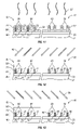
- FIG. 1 is a flowchart illustrating a method for fabricating a semiconductor device wherein stress memory is imparted to a plurality of fin structures included within the semiconductor device in accordance with a first exemplary embodiment
- FIGS. 2-19 are simplified cross-sectional views of an exemplary semiconductor device including complementary FinFETs at various stages of fabrication and produced in accordance with the exemplary method illustrated in FIG. 1 .
- FIG. 1 is a flowchart illustrating an exemplary method for fabricating a non-planar semiconductor device in which stress memory is imparted to one or more raised crystalline structures, such as a plurality of fin structures.
- the exemplary method shown in FIG. 1 is described below in conjunction with an exemplary semiconductor device 40 , 42 including two complementary non-planar transistors, namely, a P-type FinFET 40 and an N-type FinFET 42 .
- FIGS. 2-16 also described below, are simplified cross-sectional views of semiconductor device 40 , 42 illustrating P-type FinFET 40 and N-type FinFET 42 at various stages of fabrication and produced in accordance with the exemplary fabrication method shown in FIG. 1 .
- non-planar semiconductor devices e.g., triFETs
- fin structure or other raised crystalline structure
- the exemplary semiconductor fabrication method commences with the formation of at least one plurality of fin structures.
- a first plurality of fin structures included within P-type FinFET 40 and a second plurality of fin structures included within N-type FinFET 42 are formed overlying a semiconductor substrate 46 as illustrated in FIG. 2 .
- Semiconductor substrate 46 is preferably a silicon substrate (the term “silicon substrate” encompassing the relatively pure silicon materials typically used in the semiconductor industry as well as silicon admixed with other elements, such as germanium and the like).
- Semiconductor substrate 46 can be a bulk silicon wafer. However, as indicated in FIG.
- semiconductor substrate 46 preferably assumes the form a silicon-on-insulator wafer including a thin layer of silicon 48 overlying an intermediate insulating layer 50 that is, in turn, supported by a silicon carrier wafer 52 .
- a mandrel-forming layer 54 is formed over upper silicon layer 48 of semiconductor substrate 46 utilizing a known deposition technique, such as chemical vapor deposition.
- a non-exhaustive list of materials that can be deposited to form mandrel-forming layer 54 includes polycrystalline silicon, silicon oxynitride, silicon oxide, and silicon nitride.
- One or more intervening layers can also be formed between mandrel-forming layer 54 and upper silicon layer 48 of semiconductor substrate 46 ; for example, a silicon nitride layer 56 may be formed between mandrel-forming layer 54 and upper silicon layer 48 as indicated in FIG. 2 .
- selected portions of mandrel-forming layer 54 are next removed to create a number of sacrificial mandrels 58 overlying semiconductor substrate 46 .
- the selected portions of mandrel-forming layer 54 can be removed by first depositing photoresist over mandrel-forming layer 54 , patterning the photoresist, etching the portions of mandrel-forming layer 54 exposed through the patterned photoresist, and subsequently removing the patterned photoresist. If desired, a plasma etching process can be utilized to remove the portions of mandrel-forming layer 54 exposed through the patterned photoresist or other mask.
- a reactive ion etch process can be performed utilizing a chemistry selective to mandrel-forming layer 54 .
- a chemistry selective to mandrel-forming layer 54 For example, if mandrel-forming layer 54 is formed from silicon nitride, a trifluoride/oxygen chemistry can be utilized; if mandrel-forming layer 54 is formed from silicon oxynitride or silicon oxide, a carbon hydro-trifluoride or tetrafluoromethane chemistry can be utilized; and if mandrel-forming layer 54 is formed from polycrystalline silicon, a chloride or bromous acid chemistry can be utilized.
- a spacer-forming layer 60 is deposited over sacrificial mandrels 58 and silicon nitride layer 56 as further illustrated in FIG. 3 .
- Spacer-forming layer 60 is conveniently formed via the blanket deposition of silicon nitride, silicon oxide, or another dielectric material.
- the composition of spacer-forming layer 60 is chosen to permit sacrificial mandrels 58 to be removed via a subsequent etching process that is selective to mandrel-forming layer 54 over spacer-forming layer 60 ; e.g., mandrel-forming layer 54 and spacer-forming layer 60 may comprise silicon nitride and silicon oxide, respectively, thereby permitting sacrificial mandrels formed from mandrel-forming layer 54 to be selectively removed utilizing a hot phosphoric acid wet etch.
- spacer-forming layer 60 is deposited to a thickness of approximately 15 nanometers (nm) to approximately 40 nm.
- partially-completed semiconductor device 40 , 42 is subjected to a series of sequential etching steps.
- an anisotropic or directional etch is first performed to remove selected portions of spacer-forming layer 60 and create sidewall spacers 62 adjacent opposing sides of each sacrificial mandrel 58 .
- FIG. 4 an anisotropic or directional etch is first performed to remove selected portions of spacer-forming layer 60 and create sidewall spacers 62 adjacent opposing sides of each sacrificial mandrel 58 .
- a second etching process is then performed to selectively remove sacrificial mandrels 58 while generally leaving intact sidewall spacers 62 ; e.g., as previously stated, sacrificial mandrels 58 can be selectively removed utilizing a hot phosphoric acid wet etch in embodiments wherein sacrificial mandrels 58 and sidewall spacers 62 are formed from silicon nitride and silicon oxide, respectively.
- one or more additional etching steps are performed to remove the portions of silicon nitride layer 56 and upper silicon layer 48 that are not located beneath sidewall spacers 62 . As illustrated in FIG.
- the performance of these latter etching steps results in the formation of a plurality of fin structures 64 overly insulating layer 50 of semiconductor substrate 46 .
- a silicon nitride cap 66 formed from silicon nitride layer 56 overlies each fin structure 64 .
- sidewall spacers 62 are removed utilizing either a wet or dry etching process.
- a chemistry selective to sidewall spacers 62 is preferably employed during the selected etching process to minimize erosion of fin structures 64 ; e.g., if sidewall spacers 62 comprise silicon oxide, a carbon hydro-trifluoride or tetrafluoromethane chemistry can be utilized.
- first and second patterned ion implantation processes are performed to amorphize opposing outer portions of fin structures 64 of P-type FinFET 40 . More specifically, as indicated in FIG. 8 at 71 , a first ion implantation process is performed to selectively amorphize a first sidewall portion 72 of each fin structure 64 included within P-type FinFET 40 .
- a mask 70 is positioned over N-type FinFET 42 to prevent the amphorization of fin structures 64 included within N-type FinFET 42 during the performance of STEP 68 ( FIG. 1 ).
- semiconductor device 40 , 42 is bombarded with ions from a first predetermined direction that forms a first predetermined acute grazing angle with the upper surface of semiconductor substrate 46 .
- a second ion implantation process is subsequently performed with mask 70 in place to selectively amorphize a second opposing sidewall portion 74 of each fin structure 64 included within P-type FinFET 40 .
- P-type FinFET 40 is bombarded with ions from a second predetermined direction that forms a second predetermined acute grazing angle with the upper surface of semiconductor substrate 46 .
- the first and second predetermined directions are preferably rotationally offset by approximately 180 degrees, as rotated about an axis normal to semiconductor substrate 46 .
- the first patterned ion implantation is first performed, semiconductor device 40 , 42 is rotated by 180 degrees, and then the second patterned ion implantation is performed.
- the first and second predetermined acute grazing angles are preferably substantially equivalent and may each be, for example, approximately 45 degrees.
- first and second ion implantation processes are performed during STEP 68 ( FIG. 1 ) to amorphize opposing outer portions of each fin structure 64 included within P-type FinFET 40 .
- the angle and energy of the ion implantation process or processes can be controlled such that any desired portion of each fin structure 64 included within P-type FinFET 40 is amorphized during STEP 68 of the exemplary semiconductor fabrication method shown in FIG. 1 .
- the ion implantation process or processes can be controlled such that an upper portion, a lower portion, or an inner portion of each fin structure 64 is amorphized during STEP 68 ( FIG. 1 ).
- each fin structure 64 can be amorphized during STEP 68 , providing that a sufficient number of seed crystals are left in their original state to permit the amorphized portions of fin structure 64 to be recrystallized during the subsequent annealing process (described below).
- fin structures 64 are implanted with at least one electrically neutral amphorizing species of ion that generally does not affect the electrical characteristics of the channel region.
- electrically neutral amphorizing species include, but are not limited to, argon, silicon, and xenon. It is also generally preferred that implantation of the selected amphorizing species is controlled so as to avoid significant doping of semiconductor substrate 46 and thereby permit substrate 46 to be doped independently at a later juncture in the semiconductor fabrication process.
- First sacrificial strain layer 78 may comprise any one of a number of strain materials conventionally utilized in the semiconductor industry and capable of applying either a tensile or compressive stress to amorphized portions 72 , 74 of fin structures 64 sufficient to induce a physical deformation with the crystal lattice thereof. As shown in FIG. 10 , first sacrificial strain layer 78 overlies, and acts directly upon, three sides of each fin structure 64 included within P-type FinFET 40 .
- first sacrificial strain layer 78 induces strain within amorphized portions 72 , 74 of each fin structure 64 in a highly effective manner as compared to certain conventional stress memorization techniques wherein only a single side of a channel region is exposed directly to a strain material, such as in the above-described case of a deposited strained silicon nitride contact etch stop over a merged fin source-drain.
- Fin structures 64 of N-type FinFET 42 which do not include any amorphized regions at this juncture in the fabrication process, are substantially unaffected by application of sacrificial strain layer 78 during STEP 76 ( FIG. 1 ).
- first sacrificial strain layer 78 will generally depend upon device characteristics; e.g., in the case of a non-planar transistor, the type of material will typically be chosen based, at least in part, upon transistor polarity.
- the sacrificial strain layer is formed from compressive strain material, such as compressive nitride, when stress is to be applied to the channel region of a P-type transistor; and from a tensile strain material, such as tensile nitride, when stress is to be applied to the channel region of an N-type transistor.
- first sacrificial strain layer 78 is utilized to apply stress to fin structures 64 of P-type FinFET 40
- first sacrificial strain layer 78 preferably comprises compressive nitride. Further discussion of the various types of strain material that can be utilized to induce strain within the fin structures of one or more non-planar semiconductor devices, such as P-type FinFET 40 and N-type FinFET 42 , is set-forth below in conjunction with STEP 88 of the exemplary semiconductor fabrication method shown in FIG. 1 .
- semiconductor device 40 , 42 is subjected to one or more annealing steps (STEP 80 , FIG. 1 ).
- amorphized portions 72 , 74 of fin structures 64 recrystallize to accommodate the deformation induced by sacrificial strain layer 78 ; for example, if sacrificial strain layer 78 comprises compressive nitride, amorphized portions 72 , 74 of fin structures 64 will recrystallize to accommodate the tensile deformation induced by strain layer 98 .
- Annealing thus results in the recrystallization of amorphized portions 92 , 94 of fin structures 64 in a stress memorized state.
- sacrificial strain layer 78 can be removed (STEP 80 , FIG. 1 ) and amorphized portions 72 , 74 of first sacrificial strain layer 78 will retain a strain-induced deformation and a corresponding increase in carrier mobility.
- the manner in which sacrificial strain layer 78 is removed will vary depending upon the material utilized to form strain layer 78 . For example, if formed from compressive or tensile nitride as previously suggested, sacrificial strain layer 78 can be removed utilizing either hot phosphoric acid wet etch or a reactive ion etch in conjunction with a chlorine- or fluorine-based chemistry. Annealing of semiconductor device 40 , 42 also helps heal any damage inflicted to the crystal lattice of fin structures 64 during previous ion implantation processes (STEP 68 , FIG. 1 ).
- the fabrication method may proceed directly to the performance of conventional processing steps to complete fabrication of the semiconductor device after stress memory has been imparted to a single non-planar transistor or group of non-planar transistors included within the semiconductor device.
- additional steps may be performed to impart stress memory to the second transistor.
- several additional steps i.e., STEPS 86 , 88 , 90 ) are performed to impart stress memory to N-type FinFET 42 as illustrated in FIGS. 12-16 .
- STEPS 86 , 88 , and 90 are similar to STEPS 68 , 76 , and 80 performed to impart stress memory to P-type FinFET 40 as described above.
- a second patterned implant is performed to amorphize at least one portion of each fin structure 64 included within N-type FinFET 42 .
- a first angled ion implantation process is first performed to amorphize a first sidewall portion 92 of each fin structure 64 included within N-type FinFET 42 as illustrated generically in FIG. 12 at 93 .
- STEP 86 FIG.
- a second angled ion implantation is subsequently performed to amorphize a first sidewall portion 92 of each fin structure 64 included within N-type FinFET 42 as illustrated generically in FIG. 13 at 95 .
- Semiconductor device 40 , 42 is bombarded with ions from a first predetermined direction during the first ion implantation process ( FIG. 12 ) and from a second predetermined direction substantially opposite the first predetermined direction during the second ion implantation process ( FIG. 13 ).
- a mask 96 is positioned over P-type FinFET 40 to prevent amphorization of fin structures 64 included within P-type FinFET 40 during the ion implantation processes.
- the ion implantation processes can controlled such that other regions of fin structures 64 (e.g., inner regions of fin structures 64 ) are amorphized in alternative embodiments in addition to, or in lieu of, opposing sidewall portions 92 and 94 of fin structures 64 .
- second sacrificial strain layer 98 is blanket deposited over semiconductor device 40 , 42 .
- second sacrificial strain layer 98 may comprise any material capable of applying either a compressive or tensile stress to fin structures 64 sufficient to physically deform within the crystal lattice of amorphized portions 92 , 94 and thereby improve carrier mobility.
- second sacrificial strain layer 98 overlies, and acts directly upon, three sides of each fin structure 64 included within N-type FinFET 42 ; consequently, sacrificial strain layer 98 applies stress to and induces strain within amorphized portions 92 , 94 of sacrificial strain layer 98 in a highly effective manner.
- second sacrificial strain layer 98 is formed from a strain material having a polarity opposite the strain material from which first sacrificial strain layer 78 is formed; e.g., in embodiments wherein first sacrificial strain layer 78 is formed from compressive nitride, second sacrificial strain layer 98 is preferably formed from tensile nitride.
- first sacrificial strain layer 78 is formed from compressive nitride
- second sacrificial strain layer 98 is preferably formed from tensile nitride.
- a first strain material that applies a greater compressive stress can be utilized to induce strain within a first transistor, while a second strain material that applies a lesser compressive stress can be utilized to induce strain within a second complementary transistor.
- a neutral strain material e.g., neutral nitride
- semiconductor device 40 , 42 is next subjected to one or annealing steps to recrystallize amorphized portions 92 , 94 of fin structures 64 in a stress-memorized state (STEP 90 , FIG. 1 ).
- amorphized portions 92 , 94 of fin structures 64 recrystallize to accommodate the deformation induced by sacrificial strain layer 98 ; for example, if sacrificial strain layer 98 comprises tensile nitride, amorphized portions 92 , 94 of fin structures 64 will recrystallize to accommodate the compressive deformation induced by layer 98 .
- second sacrificial strain layer 98 can then be removed utilizing either a wet etching process (e.g., a hot phosphoric acid wet etch) or a dry etching process (e.g., reactive ion etch) to yield a partially completed semiconductor device 40 , 42 having improved carrier mobility in the channel regions of P-type FinFET 40 and in the channel regions of N-type FinFET 42 .
- a wet etching process e.g., a hot phosphoric acid wet etch
- a dry etching process e.g., reactive ion etch
- additional steps are performed to complete processing of semiconductor device 40 , 42 .
- the additional steps include the formation of one or more gate stacks overlying fin structures 64 of P-type FinFET 40 and N-type FinFET 42 .
- a gate insulator layer 104 can be formed over fin structures 64 and the upper surface of semiconductor substrate 46 .
- gate insulator layer 104 can comprise a high-k dielectric material deposited over fin structures 64 and the exposed upper surface of semiconductor substrate 46 utilizing a vapor deposition process, such as chemical vapor deposition (CVD), low pressure chemical vapor deposition (LPCVD), or plasma enhanced chemical vapor deposition (PECVD).
- CVD chemical vapor deposition
- LPCVD low pressure chemical vapor deposition
- PECVD plasma enhanced chemical vapor deposition
- a non-exhaustive list of high-k dielectric materials that may be deposited to form gate insulator layer 104 includes hafnium dioxide, hafnium silicon oxide, titanium dioxide, tantalum pentoxide, zirconium dioxide, and various other compounds that have a relatively high dielectric constant as compared to silicon dioxide or silicon oxynitride.
- a conductive gate electrode layer 106 is next deposited over gate insulator layer 104 utilizing a conventional deposition technique, such as CVD, LPCVD, or PECVD.
- a conventional deposition technique such as CVD, LPCVD, or PECVD.
- conductive materials suitable for use in the formation of gate electrode layer 106 includes a polycrystalline silicon and various metals and alloys, such as titanium nitride, tantalum nitride, hafnium silicide, and tantalum carbide.
- one or more mask layers are formed over gate electrode layer 106 .
- a single nitride capping layer 108 is deposited over conductive gate electrode layer 106 .
- Nitride capping layer 108 can comprise silicon nitride deposited over gate electrode layer 106 utilizing a low temperature deposition process, such as PECVD, performed utilizing silane, ammonia, and/or nitrogen in the presence of an argon plasma.
- PECVD low temperature deposition process
- a photoresist layer 110 ( FIG. 17 ) is next deposited over nitride capping layer 108 and patterned utilizing a photolithography process.
- FIG. 18 which is a cross-sectional view of P-type FinFET 40 taken along line 18 - 18 (identified in FIG. 17 )
- photolithography of photoresist layer 110 creates at least one mask structure 112 along the upper surface of nitride capping layer 108 .
- one or more etching processes are then performed to define at least one gate stack 114 from the portions of nitride capping layer 108 , conductive gate electrode layer 106 , and gate insulator layer 104 that are not located beneath mask structure 112 .
- gate stack 114 includes: (i) a nitride cap 116 formed from nitride capping layer 108 , (ii) a conductive gate electrode 118 formed from gate electrode layer 106 , and (iii) a gate insulator 120 formed from gate insulator layer 104 .
- mask structure 112 FIG. 18
- a similar gate stack is also formed overlying fin structures 64 of N-type FinFET 42 ( FIG. 17 ).
- a non-planar semiconductor device such as a FinFET
- stress memory is effectively imparted to one or more fin structures included within the non-planar semiconductor device. While the foregoing exemplary embodiment was described above in conjunction with a particular type of non-planar semiconductor device (i.e., a FinFET), embodiments of the exemplary method are equally applicable to other types of non-planar devices including other types of non-planar, multi-gate semiconductor devices, such as triFETs.
- a first patterned ion implantation process and a first blanket strain layer deposition were performed to selectively impart stress to the amorphized portions of the fin structures included within an N-type transistor (i.e., FinFET 40 shown in FIGS. 2-19 ), and a second patterned ion implantation process and a second blanket strain layer deposition were performed to selectively impart stress to the amorphized portions of the fin structures included within a P-type transistor (i.e., FinFET 42 shown in FIGS. 2-17 ).
- a blanket ion implantation step can be performed to simultaneously amorphized one or more selected portion of the fin structures included within a P-type transistor and the fin structures included within a N-type transistor.
- a first layer of strain material e.g., compressive nitride
- a second layer of strain material e.g., tensile nitride
- a single annealing step can be performed to recrystallize the amorphized portions of the N-type transistor and the P-type transistor in a stress memorized state thereby reducing the overall thermal budget of the semiconductor fabrication process.
Abstract
Description
Claims (4)
Priority Applications (1)
| Application Number | Priority Date | Filing Date | Title |
|---|---|---|---|
| US12/512,814 US8039349B2 (en) | 2009-07-30 | 2009-07-30 | Methods for fabricating non-planar semiconductor devices having stress memory |
Applications Claiming Priority (1)
| Application Number | Priority Date | Filing Date | Title |
|---|---|---|---|
| US12/512,814 US8039349B2 (en) | 2009-07-30 | 2009-07-30 | Methods for fabricating non-planar semiconductor devices having stress memory |
Publications (2)
| Publication Number | Publication Date |
|---|---|
| US20110027978A1 US20110027978A1 (en) | 2011-02-03 |
| US8039349B2 true US8039349B2 (en) | 2011-10-18 |
Family
ID=43527437
Family Applications (1)
| Application Number | Title | Priority Date | Filing Date |
|---|---|---|---|
| US12/512,814 Expired - Fee Related US8039349B2 (en) | 2009-07-30 | 2009-07-30 | Methods for fabricating non-planar semiconductor devices having stress memory |
Country Status (1)
| Country | Link |
|---|---|
| US (1) | US8039349B2 (en) |
Cited By (5)
| Publication number | Priority date | Publication date | Assignee | Title |
|---|---|---|---|---|
| US20120295430A1 (en) * | 2009-04-24 | 2012-11-22 | Varian Semiconductor Equipment Associates, Inc. | Method for processing a substrate having a non-planar substrate surface |
| US8896063B2 (en) | 2013-04-18 | 2014-11-25 | International Business Machines Corporation | FinFET devices containing merged epitaxial Fin-containing contact regions |
| US9024355B2 (en) | 2012-05-30 | 2015-05-05 | International Business Machines Corporation | Embedded planar source/drain stressors for a finFET including a plurality of fins |
| US9905694B2 (en) * | 2016-07-20 | 2018-02-27 | Globalfoundries Inc. | Fin-type field-effect transistors with strained channels |
| US20200258886A1 (en) * | 2019-02-07 | 2020-08-13 | Micron Technology, Inc. | Atom implantation for passivation of pillar material |
Families Citing this family (11)
| Publication number | Priority date | Publication date | Assignee | Title |
|---|---|---|---|---|
| US8952429B2 (en) * | 2010-09-15 | 2015-02-10 | Institute of Microelectronics, Chinese Academy of Sciences | Transistor and method for forming the same |
| US8900973B2 (en) * | 2011-08-30 | 2014-12-02 | International Business Machines Corporation | Method to enable compressively strained pFET channel in a FinFET structure by implant and thermal diffusion |
| CN103021850B (en) * | 2011-09-20 | 2015-04-15 | 中国科学院微电子研究所 | Semiconductor structure and manufacturing method thereof |
| US20130237026A1 (en) | 2012-03-09 | 2013-09-12 | Taiwan Semiconductor Manufacturing Company, Ltd., ("Tsmc") | Finfet device having a strained region |
| EP2741320B1 (en) * | 2012-12-05 | 2020-06-17 | IMEC vzw | Manufacturing method of a finfet device with dual-strained channels |
| US20150097270A1 (en) * | 2013-10-07 | 2015-04-09 | International Business Machines Corporation | Finfet with relaxed silicon-germanium fins |
| US9607901B2 (en) * | 2015-05-06 | 2017-03-28 | Stmicroelectronics, Inc. | Integrated tensile strained silicon NFET and compressive strained silicon-germanium PFET implemented in FINFET technology |
| FR3073976B1 (en) | 2017-11-23 | 2019-12-27 | Commissariat A L'energie Atomique Et Aux Energies Alternatives | METHOD FOR MANUFACTURING COUPLES OF LOW TEMPERATURE "END-FET" CMOS TRANSISTORS |
| CN110323136B (en) * | 2018-03-29 | 2023-06-13 | 中芯国际集成电路制造(上海)有限公司 | FinFET manufacturing process |
| US11450571B2 (en) * | 2018-09-27 | 2022-09-20 | Taiwan Semiconductor Manufacturing Company Ltd. | Method for manufacturing semiconductor structure |
| US10879132B2 (en) * | 2019-05-29 | 2020-12-29 | International Business Machines Corporation | Combination of tensilely strained n-type fin field effect transistors and compressively strained p-type fin field effect transistors |
Citations (5)
| Publication number | Priority date | Publication date | Assignee | Title |
|---|---|---|---|---|
| US20060076643A1 (en) * | 2004-10-08 | 2006-04-13 | Internationall Business Machines Corporation | Fin-type antifuse |
| US20070105299A1 (en) * | 2005-11-10 | 2007-05-10 | International Business Machines Corporation | Dual stress memory technique method and related structure |
| US20070249130A1 (en) * | 2006-04-21 | 2007-10-25 | Anderson Brent A | Finfet/trigate stress-memorization method |
| US20090072276A1 (en) * | 2007-08-24 | 2009-03-19 | Kabushiki Kaisha Toshiba | Semiconductor wafer, semiconductor device and method of fabricating the same |
| US20090114955A1 (en) * | 2007-11-02 | 2009-05-07 | Chris Stapelmann | Method for Fabricating a Fin-Shaped Semiconductor Structure and a Fin-Shaped Semiconductor Structure |
-
2009
- 2009-07-30 US US12/512,814 patent/US8039349B2/en not_active Expired - Fee Related
Patent Citations (5)
| Publication number | Priority date | Publication date | Assignee | Title |
|---|---|---|---|---|
| US20060076643A1 (en) * | 2004-10-08 | 2006-04-13 | Internationall Business Machines Corporation | Fin-type antifuse |
| US20070105299A1 (en) * | 2005-11-10 | 2007-05-10 | International Business Machines Corporation | Dual stress memory technique method and related structure |
| US20070249130A1 (en) * | 2006-04-21 | 2007-10-25 | Anderson Brent A | Finfet/trigate stress-memorization method |
| US20090072276A1 (en) * | 2007-08-24 | 2009-03-19 | Kabushiki Kaisha Toshiba | Semiconductor wafer, semiconductor device and method of fabricating the same |
| US20090114955A1 (en) * | 2007-11-02 | 2009-05-07 | Chris Stapelmann | Method for Fabricating a Fin-Shaped Semiconductor Structure and a Fin-Shaped Semiconductor Structure |
Cited By (9)
| Publication number | Priority date | Publication date | Assignee | Title |
|---|---|---|---|---|
| US20120295430A1 (en) * | 2009-04-24 | 2012-11-22 | Varian Semiconductor Equipment Associates, Inc. | Method for processing a substrate having a non-planar substrate surface |
| US8507372B2 (en) * | 2009-04-24 | 2013-08-13 | Varian Semiconductor Equipment Associates, Inc. | Method for processing a substrate having a non-planar substrate surface |
| US9024355B2 (en) | 2012-05-30 | 2015-05-05 | International Business Machines Corporation | Embedded planar source/drain stressors for a finFET including a plurality of fins |
| US9443951B2 (en) | 2012-05-30 | 2016-09-13 | Globalfoundries Inc. | Embedded planar source/drain stressors for a finFET including a plurality of fins |
| US8896063B2 (en) | 2013-04-18 | 2014-11-25 | International Business Machines Corporation | FinFET devices containing merged epitaxial Fin-containing contact regions |
| US8900934B2 (en) | 2013-04-18 | 2014-12-02 | International Business Machines Corporation | FinFET devices containing merged epitaxial Fin-containing contact regions |
| US9905694B2 (en) * | 2016-07-20 | 2018-02-27 | Globalfoundries Inc. | Fin-type field-effect transistors with strained channels |
| US20200258886A1 (en) * | 2019-02-07 | 2020-08-13 | Micron Technology, Inc. | Atom implantation for passivation of pillar material |
| US11164876B2 (en) * | 2019-02-07 | 2021-11-02 | Micron Technology, Inc. | Atom implantation for passivation of pillar material |
Also Published As
| Publication number | Publication date |
|---|---|
| US20110027978A1 (en) | 2011-02-03 |
Similar Documents
| Publication | Publication Date | Title |
|---|---|---|
| US8039349B2 (en) | Methods for fabricating non-planar semiconductor devices having stress memory | |
| US8192641B2 (en) | Methods for fabricating non-planar electronic devices having sidewall spacers formed adjacent selected surfaces | |
| US9023697B2 (en) | 3D transistor channel mobility enhancement | |
| KR101558061B1 (en) | Finfets and methods for forming the same | |
| US7449753B2 (en) | Write margin improvement for SRAM cells with SiGe stressors | |
| US7977174B2 (en) | FinFET structures with stress-inducing source/drain-forming spacers and methods for fabricating the same | |
| US9196694B2 (en) | Integrated circuits with dual silicide contacts and methods for fabricating same | |
| US7494878B2 (en) | Metal-oxide-semiconductor transistor and method of forming the same | |
| US7759205B1 (en) | Methods for fabricating semiconductor devices minimizing under-oxide regrowth | |
| US20110084336A1 (en) | Semiconductor device with stressed fin sections, and related fabrication methods | |
| WO2005122276A1 (en) | Semiconductor device and manufacturing method thereof | |
| TW200532855A (en) | Slim spacer device and manufacturing method | |
| US20100308409A1 (en) | Finfet structures with fins having stress-inducing caps and methods for fabricating the same | |
| US9306036B2 (en) | Nitride spacer for protecting a fin-shaped field effect transistor (finFET) device | |
| JP2009105122A (en) | Semiconductor device and its manufacturing method | |
| CN105826203A (en) | Method of forming FinFET transistor device and FinFET transistor device | |
| US10032680B2 (en) | Strained finFET device fabrication | |
| US20110254092A1 (en) | Etsoi cmos architecture with dual backside stressors | |
| US20120153350A1 (en) | Semiconductor devices and methods for fabricating the same | |
| US8642420B2 (en) | Fabrication of a semiconductor device with extended epitaxial semiconductor regions | |
| US7157374B1 (en) | Method for removing a cap from the gate of an embedded silicon germanium semiconductor device | |
| WO2008016505A1 (en) | Method for forming a strained transistor by stress memorization based on a stressed implantation mask | |
| US8987789B2 (en) | Transistors having stressed channel regions and methods of forming transistors having stressed channel regions | |
| US9704881B2 (en) | Semiconductor device with reduced poly spacing effect | |
| US11688741B2 (en) | Gate-all-around devices with isolated and non-isolated epitaxy regions for strain engineering |
Legal Events
| Date | Code | Title | Description |
|---|---|---|---|
| AS | Assignment |
Owner name: GLOBALFOUNDRIES INC., CAYMAN ISLANDS Free format text: ASSIGNMENT OF ASSIGNORS INTEREST;ASSIGNORS:HARGROVE, MICHAEL;JOHNSON, FRANK SCOTT;LUNING, SCOTT;SIGNING DATES FROM 20090721 TO 20090805;REEL/FRAME:023125/0658 |
|
| STCF | Information on status: patent grant |
Free format text: PATENTED CASE |
|
| FPAY | Fee payment |
Year of fee payment: 4 |
|
| FEPP | Fee payment procedure |
Free format text: MAINTENANCE FEE REMINDER MAILED (ORIGINAL EVENT CODE: REM.); ENTITY STATUS OF PATENT OWNER: LARGE ENTITY |
|
| AS | Assignment |
Owner name: ALSEPHINA INNOVATIONS INC., CANADA Free format text: ASSIGNMENT OF ASSIGNORS INTEREST;ASSIGNOR:GLOBALFOUNDRIES INC.;REEL/FRAME:049709/0871 Effective date: 20181126 |
|
| LAPS | Lapse for failure to pay maintenance fees |
Free format text: PATENT EXPIRED FOR FAILURE TO PAY MAINTENANCE FEES (ORIGINAL EVENT CODE: EXP.); ENTITY STATUS OF PATENT OWNER: LARGE ENTITY |
|
| STCH | Information on status: patent discontinuation |
Free format text: PATENT EXPIRED DUE TO NONPAYMENT OF MAINTENANCE FEES UNDER 37 CFR 1.362 |
|
| FP | Expired due to failure to pay maintenance fee |
Effective date: 20191018 |
|
| AS | Assignment |
Owner name: GLOBALFOUNDRIES INC., CAYMAN ISLANDS Free format text: RELEASE BY SECURED PARTY;ASSIGNOR:WILMINGTON TRUST, NATIONAL ASSOCIATION;REEL/FRAME:054636/0001 Effective date: 20201117 |