US8041450B2 - Position sensor system for substrate transfer robot - Google Patents
Position sensor system for substrate transfer robot Download PDFInfo
- Publication number
- US8041450B2 US8041450B2 US11/867,525 US86752507A US8041450B2 US 8041450 B2 US8041450 B2 US 8041450B2 US 86752507 A US86752507 A US 86752507A US 8041450 B2 US8041450 B2 US 8041450B2
- Authority
- US
- United States
- Prior art keywords
- end effector
- substrate
- sensor
- emitter
- sensors
- Prior art date
- Legal status (The legal status is an assumption and is not a legal conclusion. Google has not performed a legal analysis and makes no representation as to the accuracy of the status listed.)
- Active, expires
Links
Images


Classifications
-
- H—ELECTRICITY
- H01—ELECTRIC ELEMENTS
- H01L—SEMICONDUCTOR DEVICES NOT COVERED BY CLASS H10
- H01L21/00—Processes or apparatus adapted for the manufacture or treatment of semiconductor or solid state devices or of parts thereof
- H01L21/67—Apparatus specially adapted for handling semiconductor or electric solid state devices during manufacture or treatment thereof; Apparatus specially adapted for handling wafers during manufacture or treatment of semiconductor or electric solid state devices or components ; Apparatus not specifically provided for elsewhere
- H01L21/67005—Apparatus not specifically provided for elsewhere
- H01L21/67242—Apparatus for monitoring, sorting or marking
- H01L21/67259—Position monitoring, e.g. misposition detection or presence detection
- H01L21/67265—Position monitoring, e.g. misposition detection or presence detection of substrates stored in a container, a magazine, a carrier, a boat or the like
-
- B—PERFORMING OPERATIONS; TRANSPORTING
- B25—HAND TOOLS; PORTABLE POWER-DRIVEN TOOLS; MANIPULATORS
- B25J—MANIPULATORS; CHAMBERS PROVIDED WITH MANIPULATION DEVICES
- B25J11/00—Manipulators not otherwise provided for
- B25J11/0095—Manipulators transporting wafers
-
- B—PERFORMING OPERATIONS; TRANSPORTING
- B25—HAND TOOLS; PORTABLE POWER-DRIVEN TOOLS; MANIPULATORS
- B25J—MANIPULATORS; CHAMBERS PROVIDED WITH MANIPULATION DEVICES
- B25J19/00—Accessories fitted to manipulators, e.g. for monitoring, for viewing; Safety devices combined with or specially adapted for use in connection with manipulators
- B25J19/02—Sensing devices
- B25J19/021—Optical sensing devices
-
- H—ELECTRICITY
- H01—ELECTRIC ELEMENTS
- H01L—SEMICONDUCTOR DEVICES NOT COVERED BY CLASS H10
- H01L21/00—Processes or apparatus adapted for the manufacture or treatment of semiconductor or solid state devices or of parts thereof
- H01L21/67—Apparatus specially adapted for handling semiconductor or electric solid state devices during manufacture or treatment thereof; Apparatus specially adapted for handling wafers during manufacture or treatment of semiconductor or electric solid state devices or components ; Apparatus not specifically provided for elsewhere
- H01L21/677—Apparatus specially adapted for handling semiconductor or electric solid state devices during manufacture or treatment thereof; Apparatus specially adapted for handling wafers during manufacture or treatment of semiconductor or electric solid state devices or components ; Apparatus not specifically provided for elsewhere for conveying, e.g. between different workstations
- H01L21/67739—Apparatus specially adapted for handling semiconductor or electric solid state devices during manufacture or treatment thereof; Apparatus specially adapted for handling wafers during manufacture or treatment of semiconductor or electric solid state devices or components ; Apparatus not specifically provided for elsewhere for conveying, e.g. between different workstations into and out of processing chamber
- H01L21/67742—Mechanical parts of transfer devices
-
- H—ELECTRICITY
- H01—ELECTRIC ELEMENTS
- H01L—SEMICONDUCTOR DEVICES NOT COVERED BY CLASS H10
- H01L21/00—Processes or apparatus adapted for the manufacture or treatment of semiconductor or solid state devices or of parts thereof
- H01L21/67—Apparatus specially adapted for handling semiconductor or electric solid state devices during manufacture or treatment thereof; Apparatus specially adapted for handling wafers during manufacture or treatment of semiconductor or electric solid state devices or components ; Apparatus not specifically provided for elsewhere
- H01L21/68—Apparatus specially adapted for handling semiconductor or electric solid state devices during manufacture or treatment thereof; Apparatus specially adapted for handling wafers during manufacture or treatment of semiconductor or electric solid state devices or components ; Apparatus not specifically provided for elsewhere for positioning, orientation or alignment
- H01L21/681—Apparatus specially adapted for handling semiconductor or electric solid state devices during manufacture or treatment thereof; Apparatus specially adapted for handling wafers during manufacture or treatment of semiconductor or electric solid state devices or components ; Apparatus not specifically provided for elsewhere for positioning, orientation or alignment using optical controlling means
-
- H—ELECTRICITY
- H01—ELECTRIC ELEMENTS
- H01L—SEMICONDUCTOR DEVICES NOT COVERED BY CLASS H10
- H01L21/00—Processes or apparatus adapted for the manufacture or treatment of semiconductor or solid state devices or of parts thereof
- H01L21/67—Apparatus specially adapted for handling semiconductor or electric solid state devices during manufacture or treatment thereof; Apparatus specially adapted for handling wafers during manufacture or treatment of semiconductor or electric solid state devices or components ; Apparatus not specifically provided for elsewhere
- H01L21/683—Apparatus specially adapted for handling semiconductor or electric solid state devices during manufacture or treatment thereof; Apparatus specially adapted for handling wafers during manufacture or treatment of semiconductor or electric solid state devices or components ; Apparatus not specifically provided for elsewhere for supporting or gripping
- H01L21/687—Apparatus specially adapted for handling semiconductor or electric solid state devices during manufacture or treatment thereof; Apparatus specially adapted for handling wafers during manufacture or treatment of semiconductor or electric solid state devices or components ; Apparatus not specifically provided for elsewhere for supporting or gripping using mechanical means, e.g. chucks, clamps or pinches
- H01L21/68707—Apparatus specially adapted for handling semiconductor or electric solid state devices during manufacture or treatment thereof; Apparatus specially adapted for handling wafers during manufacture or treatment of semiconductor or electric solid state devices or components ; Apparatus not specifically provided for elsewhere for supporting or gripping using mechanical means, e.g. chucks, clamps or pinches the wafers being placed on a robot blade, or gripped by a gripper for conveyance
-
- Y—GENERAL TAGGING OF NEW TECHNOLOGICAL DEVELOPMENTS; GENERAL TAGGING OF CROSS-SECTIONAL TECHNOLOGIES SPANNING OVER SEVERAL SECTIONS OF THE IPC; TECHNICAL SUBJECTS COVERED BY FORMER USPC CROSS-REFERENCE ART COLLECTIONS [XRACs] AND DIGESTS
- Y10—TECHNICAL SUBJECTS COVERED BY FORMER USPC
- Y10S—TECHNICAL SUBJECTS COVERED BY FORMER USPC CROSS-REFERENCE ART COLLECTIONS [XRACs] AND DIGESTS
- Y10S414/00—Material or article handling
- Y10S414/135—Associated with semiconductor wafer handling
- Y10S414/141—Associated with semiconductor wafer handling includes means for gripping wafer
Definitions
- the present application relates generally to substrate processing and, more particularly, to methods and apparatuses for transferring substrates through a substrate processing system.
- An apparatus for processing semiconductor substrates typically includes a processing chamber in which the substrates are processed, a substrate handling chamber through which the substrates are moved before and after processing in the processing chamber, and one or more input/output chambers that store substrates before and after the substrates are moved through the handling chamber.
- a substrate transfer robot is located within the handling chamber and is configured to transfer substrates to and from a plurality of stations. Such stations may be within the handling chamber, the input/output chambers, the processing chamber, or other chambers.
- a typical station within the processing chamber is a substrate holder, such as a susceptor, which supports a substrate during processing.
- a station within the input/output chamber may comprise a cassette that holds a plurality of substrates.
- the input/output chambers may be loading chambers or load ports that contain substrate cassettes that are accessible by the transfer robot.
- the input/output chambers can also be load-lock chambers in which substrates can be atmospherically isolated and purged of particulates before being moved into the handling chamber and eventually into the processing chamber.
- Other stations which can be inside separate chambers or even within the substrate handling chamber, may include pre-processing stations (such as a wafer pre-cleaning station) and/or post-processing stations (such as a cooling station).
- the substrate transfer robot typically includes an actuator, one or more interlinked arms, and an end effector attached to the arms.
- the actuator is configured to move the arms and the end effector.
- the end effector is adapted to pick up a substrate from a station, hold the substrate as the robot moves the end effector and the substrate to another station, and place the substrate at another station.
- the apparatus includes a plurality of processing chambers each typically adjacent to the substrate handling chamber.
- the processing chambers are capable of processing substrates simultaneously, which increases the overall substrate throughput of the apparatus.
- the handling chamber may include more than one substrate transfer robot for improved substrate handling capability.
- a typical susceptor for holding a semiconductor wafer has a wafer pocket whose size is only slightly larger than that of a wafer that the susceptor is designed to support.
- a susceptor designed to support a 300 mm wafer might have a wafer pocket with a diameter of only 301 mm, providing a clearance of only 0.5 mm between the edge of the supported wafer and the pocket's perimeter wall. It is important that the wafer be centered in the pocket and not touch the pocket wall. If the wafer contacts the pocket wall, local temperature changes occur, resulting in temperature gradients across the wafer. This can cause non-uniformity in process results, as most semiconductor processing depends critically on temperature.
- substrate drift Errors in placement of the substrate relative to an end effector, known as “substrate drift,” are sometimes caused by variations in substrate position in the cassette at pickup. In other words, at pickup the end effector may attach to each substrate at a slightly different location. Substrate drift can also occur during robot movement, particularly when the robot moves fast. In addition to the aforementioned problems associated with failing to center the substrate within a susceptor pocket, substrate drift can result in damage to the substrate during placement at a substrate station, such as a wafer cassette.
- U.S. Pat. No. 7,008,802 discloses using photosensors that sense an extent to which an edge of the wafer blocks a light beam emitted by the photosensor. By measuring the extent to which the wafer edge blocks the light beams of the photosensors, the position of the wafer is calculated and compared to a pre-registered normal position to calculate an offset displacement to be applied to the robot to compensate for the calculated positioning error.
- Another reference that discloses using two photosensors to calculate a position of a wafer is Japanese Patent Laid-open No. 2005-93807.
- the present application discloses a semiconductor substrate processing apparatus, comprising a substrate handling chamber, a pair of position sensors, and a substrate transfer robot within the handling chamber.
- Each of the sensors comprises a light beam emitter configured to emit a beam of light, and a receiver configured to receive the light beam.
- the substrate transfer robot comprises an elongated end effector and a robot actuator.
- the end effector has a distal end and a proximal end.
- the end effector is configured to pick up and hold a semiconductor substrate at the distal end such that the substrate has a same expected position with respect to the end effector every time the substrate is picked up and held by the end effector.
- the robot actuator is configured to move the end effector within the handling chamber to transfer substrates among a plurality of substrate stations.
- the end effector has a length such that it is possible for an edge of a substrate held in the expected position by the end effector to partially block a light beam emitted from the emitter of one of the position sensors, while the proximal end of the end effector partially blocks a light beam emitted from the emitter of the other position sensor.
- the present application discloses a method of controlling a semiconductor substrate transfer robot.
- the method comprises providing a pair of position sensors, each sensor comprising a light beam emitter and a receiver.
- the emitter is configured to emit a beam of light
- the receiver is configured to receive the light beam from the emitter.
- the method also includes providing a substrate transfer robot within the handling chamber, providing an elongated end effector, and providing a robot actuator configured to move the end effector within the handling chamber to transfer substrates among a plurality of substrate stations.
- the end effector has a distal end and a proximal end and is configured to pick up and hold a semiconductor substrate at the distal end such that the substrate has a same expected position with respect to the end effector every time the substrate is picked up and held by the end effector.
- the end effector has a length such that it is possible for an edge of a substrate held in the expected position by the end effector to partially block a light beam emitted from the emitter of one of the position sensors, while the proximal end of the end effector partially blocks a light beam emitted from the emitter of the other position sensor.
- the present application discloses a semiconductor processing apparatus, comprising a substrate handling chamber, a second substrate chamber adjacent to the handling chamber, a port between the handling chamber and the second chamber, an end effector inside the handling chamber, a robot actuator, a position sensor, and a control system.
- the end effector comprises a paddle and a proximal clamping member.
- the paddle has a distal end defining a distal end of the end effector.
- the paddle also has one or more clamping elements adapted to clamp against an edge of a substrate supported by the paddle.
- the proximal clamping member has one or more proximal clamping elements adapted to clamp against an edge of a substrate supported by the paddle.
- the proximal clamping member is adapted to move toward and away from the distal end of the paddle to clamp and unclamp a substrate between the clamping elements of the paddle and the clamping elements of the proximal clamping member.
- the proximal clamping member also has a proximally extending structure that defines a proximal end of the end effector.
- the robot actuator is configured to move the end effector within the handling chamber to transfer substrates among a plurality of substrate stations.
- the position sensor comprises a light beam emitter configured to emit a beam of light, and a receiver configured to receive the light beam.
- the control system is programmed to instruct the robot actuator to move the end effector to a target position in which the end effector is oriented along a line extending from the sensor to the port, and in which the distal end of the paddle points toward the port.
- the control system is also programmed to determine an amount of light received by the receiver from the emitter, and to control movements of the end effector based on the measured amount of light.
- FIG. 1 is a schematic top view of a conventional semiconductor processing apparatus.
- FIG. 2 is a schematic top view of a wafer handling chamber of the conventional semiconductor processing apparatus of FIG. 1 .
- FIG. 3 is a schematic top view of an embodiment of a semiconductor processing apparatus.
- FIG. 4 is a top view of an embodiment of a substrate transfer robot.
- FIG. 5 is a cross-sectional view of an end effector of the substrate transfer robot of FIG. 4 .
- FIG. 6 is a top view of the substrate transfer robot of FIG. 4 clamping a substrate, shown in relation to a pair of position sensors.
- FIG. 7 is a schematic top view of the semiconductor processing apparatus of FIG. 3 illustrating position sensors.
- FIG. 8 is a schematic side view of a substrate or rear flag of an end effector partially impeding a light beam of a position photosensor, in accordance with an embodiment.
- FIG. 9 is a schematic view of certain relationships between a light beam of a position photosensor and a proximal end of an end effector, in accordance with an embodiment.
- FIG. 10 is a schematic view of certain relationships between a light beam of a position photosensor and a substrate held at a distal end of an end effector, in accordance with an embodiment.
- FIG. 11 is a flowchart illustrating a method of processing an output of a position sensor at the rear of an end effector.
- FIG. 12 is a flowchart illustrating a method of processing an output of a position sensor forward of an end effector.
- FIG. 13 is an illustration of an example sequence of operational steps performed by a pair of substrate transfer robots within a substrate handling chamber, in accordance with an embodiment.
- Each photosensor typically includes a light beam emitter above the end effector and oriented to emit a beam of light downwardly, and a light beam receiver below the end effector and configured to receive the beam of light from the emitter.
- the robot arms in certain positions, can block the light beams and thereby interfere with the sensors' ability to sense the substrate position.
- the substrates often overlap each other, and sometimes it is not possible to determine which substrate is being detected. Further, in some cases a photosensor's light beam is impeded by two different substrates, which results in a distorted calculation of the targeted substrate's position.
- FIG. 1 shows a conventional semiconductor processing apparatus 10 for processing semiconductor substrates, such as silicon wafers.
- the apparatus 10 includes a wafer handling chamber 12 , two processing chambers 14 , two load lock chambers 16 , two cooling chambers 18 , a front end wafer handling chamber 20 , and a load port 22 .
- the wafer handling chamber 12 includes a wafer transfer robot 26
- the front end wafer handling chamber 20 includes a wafer transfer robot 28 .
- the robot 28 collects wafers 24 from wafer collection devices, such as wafer cassettes or so-called FOUPs (front opening unified pods), at the load port 22 , and delivers the wafers 24 to the load lock chambers 16 .
- the robot 28 also delivers processed wafers 24 back to the wafer collection devices at the load port 22 .
- the load lock chambers 16 can be sealed to isolate and purge the wafers 24 prior to being moved into the handling chamber 12 , processing chambers 14 , and cooling chambers 18 .
- the robot 26 picks up the wafers 24 from the load lock chambers 16 and delivers the wafers to the processing chambers 14 and cooling chambers 18 for wafer processing.
- the robot 26 handles all of the wafer pickups and deliveries to and from the chambers 14 and 18 .
- the robot 26 includes an end effector in the form of a paddle 30 , which is configured to pickup a wafer 24 , support the wafer during a wafer transfer step, and then deliver the wafer to a target station.
- the robot 26 also includes arms 32 and 34 .
- the arm 32 has one end rotatably linked to the paddle 30 , and another end rotatably linked to an end of the arm 34 .
- the arm 34 has an opposite end rotatably linked to an elevator 36 that moves the robot 26 vertically.
- the elevator 36 can also be configured to rotate about a vertical axis to facilitate rotation of the robot 26 .
- the robot 26 is capable of moving a wafer 24 into and out of a processing chamber 14 and a cooling chamber 18 .
- FIG. 2 is a schematic top view of the conventional wafer handling chamber 12 of FIG. 1 .
- the handling chamber 12 has six target positions A, B, C, D, E, and F of a wafer, for delivery into the chambers adjacently surrounding the handling chamber 12 .
- the positions A and F are associated with the load lock chambers 16
- the positions B and E are associated with the cooling chambers 18
- the positions C and D are associated with the processing chambers 14 .
- Position photosensors 1 - 9 are located in the handling chamber 12 , at positions along the edges of wafers at target positions A-F. Each photosensor produces a vertical beam of light that will be partially impeded by a wafer in the associated target position.
- Each target position A-F has two of photosensors 1 - 9 along its edge, which is sufficient to calculate the wafer position.
- a problem with this arrangement is that the paddle 30 and arms 32 , 34 can impede the light beams emitted by the photosensors 1 - 9 , making it impossible to detect the wafer position. Also, if two or more wafer transfer robots 26 holding multiple wafers are provided in the handling chamber 12 , it is sometimes not possible to determine which wafer a particular photosensor is sensing. For example, if one robot positions a wafer roughly at target position A, and another robot positions a wafer roughly at target position F, then the light beam emitted by photosensor 2 may become partially impeded by both wafers, which will result in a distorted calculation of the position of the wafer intended to be sensed. Also, one wafer may completely block the light beam while the other wafer is correctly positioned, which will also distort the system's understanding of the wafer positions.
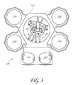
- FIG. 3 is a schematic top view of a semiconductor processing apparatus 100 for processing semiconductor substrates, such as silicon wafers, in accordance with one embodiment.
- the apparatus 100 includes a substrate handling chamber 102 , four substrate processing chambers 104 , and two input/output chambers 106 .
- the chambers 104 and 106 are preferably adjacent to the handling chamber 102 .
- the processing chambers 104 preferably include substrate holders, such as susceptors, for supporting substrates during substrate processing, such as chemical vapor deposition, atomic layer deposition, physical vapor deposition, photolithography, etching, plasma-enhanced deposition, etc.
- the processing chambers 104 can be single substrate processing chambers, or batch substrate chambers.
- the input/output chambers 106 may comprise substrate loading chambers that contain substrate collection devices, such as substrate cassettes or FOUPs.
- the input/output chambers 106 can comprise load-lock chambers in which substrates can be atmospherically isolated and purged of particulates before being moved into the handling chamber 102 and eventually into the processing chambers 104 .
- the illustrated substrate handling chamber 102 includes two substrate transfer robots 40 , such as vacuum robots, adapted to pickup, transfer, and deliver substrates among the chambers 104 and 106 .
- FIG. 4 is a top view of a substrate transfer robot 40 in accordance with one embodiment of the present application. If multiple robots 40 are provided within the substrate handling chamber 102 ( FIG. 3 ), then they are preferably configured identically.
- the illustrated robot 40 includes an elongated end effector 42 and a robot actuator 44 .
- the end effector 42 has a distal end 46 and a proximal end 48 , and is configured to pick up and hold a semiconductor substrate at the distal end 46 .
- the robot actuator 44 is configured to move the end effector 42 within the substrate handling chamber 102 to transfer substrates among a plurality of substrate stations (such as stations inside the chambers 104 and 106 ).
- the end effector 42 also referred to as a substrate clamper or wafer clamper, preferably includes a paddle 50 and a proximal clamping member 52 .
- the paddle 50 is preferably configured to underlie and support a substrate.
- the paddle 50 has two prongs 51 defining an inner slot 53 .
- the paddle 50 has no prongs 51 or slot 53 .
- the paddle 50 has a distal end that defines the distal end 46 of the end effector 42 .
- the paddle 50 has one or more forward clamping elements 54 configured to clamp against an edge of a substrate held by the end effector 42 .
- the clamping elements 54 comprise upstanding flanges. However, structures other than flanges can be used instead.
- the clamping elements 54 are at the distal end of the paddle 50 .
- the clamping elements 54 can alternatively be located somewhat rearward of the distal end of the paddle 50 .
- the paddle 50 can include spacers 55 , such as spacer pins, on which a substrate can rest.
- the illustrated paddle 50 has a proximal portion 56 comprising a sleeve 58 that is connected to the robot actuator 44 .
- the sleeve 58 houses a body portion 60 of the proximal clamping member 52 .
- the clamping member 52 preferably includes one or more clamping elements 66 configured to clamp against an edge of a substrate held by the end effector 42 .
- the clamping member 52 includes a pair of arms 62 that extend laterally and distally from the body portion 60 .
- Sidewalls of the sleeve 58 include slots 64 through which the arms 62 extend laterally and emerge from inside the sleeve 58 .
- Each arm 62 includes one clamping element 66 .
- the slots 64 are preferably slightly longer than the width of the portions of the arms 62 that extend therethrough, such that the clamping member 52 is movable toward and away from the distal end 46 of the end effector 42 .
- a linear actuator 72 can be provided for producing such movement of the clamping member 52 with respect to the sleeve 58 .
- the actuator 72 can be electrically controlled.
- the clamping member 52 preferably also includes a rear flag 68 that extends proximally through an orifice 70 of the sleeve 58 . The function of the flag 68 is discussed below.
- the illustrated robot actuator 44 includes a plurality of interlinked arms 74 .
- Two lower arms 74 have first ends rotatably linked with respect to an elevator 76 and second ends rotatably linked to an elbow member 78 .
- Two upper arms 74 have first ends rotatably linked to the elbow member 78 and second ends rotatably linked to the end effector 42 .
- the elevator 76 is preferably configured to move the robot 40 vertically and to rotate about a vertical axis with respect to a floor of the substrate handling chamber 102 ( FIG. 3 ). It will be appreciated that a variety of different types of robot actuators 44 can be provided in place of the illustrated embodiment.
- the paddle 50 is positioned underneath a substrate 80 , such that the substrate is supported on the paddle.
- the substrate 80 is supported on the spacers 55 .
- the proximal clamping member 52 is moved in a distal direction to clamp the substrate 80 between the clamping elements 54 of the paddle 50 and the clamping elements 66 of the clamping member 52 .
- the clamping member 52 is moved distally by a linear actuator 72 , described above.
- the four clamping members 54 , 66 allow the end effector 42 to hold the substrate 80 in a repeatable, expected position, shown in FIG. 6 .
- the substrate 80 has the same expected position with respect to the end effector 42 every time the substrate is picked up and held by the end effector.
- the clamping member 52 is moved in the proximal direction to unclamp the substrate.
- a preferred embodiment of the semiconductor processing apparatus 100 includes four processing chambers 104 A, 104 B, 104 C, and 104 D, and two input/output chambers 106 A and 106 B.
- each processing chamber 104 there is preferably an associated processing chamber port 108 in the wall between the handling chamber 102 and the chamber 104 .
- the illustrated handling chamber 102 includes processing chamber ports 108 A, 108 B, 108 C, and 108 D associated with processing chambers 104 A, 104 B, 104 C, and 104 D, respectively.
- Each of the processing chamber ports 108 is preferably sized to allow an end effector 42 of one of the robots 40 ( FIG. 3 ) to pass through the processing chamber port 108 while the end effector is holding a substrate in the above-described expected position associated with the end effector.
- the processing chambers 104 are provided in pairs positioned on opposing sides of the handling chamber 102 , such that their associated processing chamber ports 108 face one another.
- the apparatus 100 includes a first pair of processing chambers 104 A and 104 C, and a second pair of processing chambers 104 B and 104 D.
- the illustrated apparatus 100 also includes a first pair of processing chamber ports 108 A and 108 C, and a second pair of processing chamber ports 108 B and 108 C.
- the ports 108 A and 108 C are on opposing sides of the handling chamber 102 and face one another, and the ports 108 B and 108 D are also on opposing sides of the handling chamber 102 and also face one another.
- the apparatus 100 preferably includes a plurality of gate valves 110 each configured to isolate one of the processing chambers 104 from the handling chamber 102 .
- the apparatus 100 includes gate valves 110 A, 110 B, 110 C, and 110 D, which are configured to isolate the processing chambers 104 A, 104 B, 104 C, and 104 D, respectively, from the handling chamber 102 .
- Each gate valve 110 preferably has an open position and a closed position.
- Each gate valve 110 in its open position preferably allows an end effector 42 to pass through the gate valve 110 and through one of the processing chamber ports 108 while the end effector is holding a substrate 80 .
- Each gate valve 110 in its closed position preferably seals one of the processing chamber ports 108 .
- the apparatus 100 preferably includes a plurality of position sensors 82 each located by one of the processing chamber ports 108 , such that there is one sensor 82 for each processing chamber 104 and port 108 .
- the apparatus 100 includes position sensors 82 A, 82 B, 82 C, and 82 D within the substrate handling chamber 102 .
- the position sensors 82 are preferably provided in pairs.
- the sensors 82 A and 82 C form a first pair
- the sensors 82 B and 82 D form a second pair. The functionality of the sensors 82 is described below.
- the apparatus 100 preferably also includes input/output ports 112 between the handling chamber 102 and the input/output chambers 106 .
- the apparatus 100 includes input output ports 112 A and 112 B associated with the chambers 106 A and 106 B, respectively.
- Each input/output port 112 is preferably sized to allow an end effector 42 to pass through the input/output port while the end effector is holding a substrate in the expected position associated with the end effector.
- the apparatus 100 preferably includes a gate valve 114 for each input/output chamber 106 .
- Each gate valve 114 is preferably configured to isolate its associated input/output chamber 106 from the handling chamber 102 .
- the apparatus 100 includes gate valves 114 A and 114 B, which are configured to isolate the input/output chambers 106 A and 106 B, respectively, from the handling chamber 102 .
- Each gate valve 114 preferably has an open position and a closed position.
- Each gate valve 114 in its open position preferably allows an end effector 42 to pass through the gate valve 114 and through one of the input/output ports 112 while the end effector is holding a substrate 80 .
- Each gate valve 114 in its closed position preferably seals one of the input/output ports 112 .
- the apparatus 100 preferably includes input/output position sensors 84 each positioned on a side of the handling chamber 112 opposite one of the input/output ports 112 .
- the apparatus 100 includes input/output position sensors 84 A and 84 B.
- the sensor 84 A is positioned opposite the input/output port 112 A
- the sensor 84 B is positioned opposite the input/output port 112 B.
- the functionality of the sensors 84 is described below.
- FIG. 8 is a schematic view of a position sensor 82 or 84 in accordance with one embodiment.
- Each position sensor 82 , 84 is preferably a photosensor that comprises a light beam emitter 116 and a light beam receiver 118 .
- the emitter 116 of each sensor is positioned below the end effectors 42 ( FIG. 4 ) of the robots 40 of the substrate handling chamber 102 ( FIG. 3 ), and the receiver 118 of each sensor is positioned above the end effectors 42 and the emitter 116 .
- the emitter 116 can be mounted on a floor of the handling chamber 102
- the receiver can be mounted on a ceiling of the chamber 102 .
- the positions of the emitter 116 and receiver 118 can be reversed.
- the emitter 116 is preferably configured and oriented to emit a laser beam of light 120 toward the receiver 118
- the receiver is preferably configured to receive the light beam 120 from the emitter. In the illustrated embodiment, the emitter 116 upwardly emits the light beam 120 toward the receiver 118 .
- the ceiling and floor of the handling chamber 102 are transparent, and the emitter 116 and receiver 118 are positioned outside of the chamber 102 .
- the emitter 116 can be secured below the transparent floor of the handling chamber 102 and oriented to emit the light beam 120 through the floor into the chamber 102 .
- the receiver 118 can be secured above the transparent ceiling of the handling chamber 102 and positioned to receive the light beam 120 from the emitter 118 .
- the emitted light beam 120 preferably has a ribbon-like shape.
- the vertical dimension of the light beam 120 is its length of travel, which is the distance between the emitter 116 and the receiver 118 .
- the horizontal dimension of the illustrated light beam 120 is one of the dimensions of its transverse cross section.
- the light beam 120 preferably has a transverse cross-section whose size and shape is uniform along the length of the beam.
- the light beam 120 may be impeded by a substrate 80 held by an end effector 42 ( FIG. 6 ), or by a rear flag 68 of an end effector.
- the receiver 118 produces a voltage that is characteristic of the amount of light that reaches the receiver.
- the voltage response is preferably linear and can be inversely proportional to the area of the light beam 120 that is blocked by the substrate 80 or rear flag 68 .
- a control system 122 receives and uses the voltage signal from the receiver 118 to determine an amount of light received by the receiver 118 from its associated emitter 116 . Based on the received amount of light, the control system 122 is able to estimate the position of the substrate, as explained below.
- the control system 122 preferably monitors each of the sensors 82 and 84 in this manner. Suitable proportionate photosensors 82 and 84 are available from companies such as Keyence Corp. of Japan, LMI of Canada, and Panasonic of Japan, and are often referred to as laser through beam sensor (LTBS) systems.
- the apparatus 100 uses LX2-10 sensors produced by Keyence Corp., which have dimensions of 100 mm by 1 mm; however, this is only an example, and proportionate photosensors of different sizes may be employed.
- FIG. 6 shows an end effector 42 clamping the substrate 80 in a repeatable, expected position relative to the end effector.
- the substrate 80 has the same expected position with respect to the end effector 42 every time the substrate is picked up and held by the end effector.
- the positions of the sensors 82 and the length of each end effector 42 is preferably such that it is possible for the edge 86 of a substrate 80 held in the expected position by the end effector 42 to partially block a light beam 120 emitted from the emitter 116 of one of the position sensors 82 , while the proximal end 48 of the end effector partially blocks a light beam 120 emitted from the emitter 116 of the other position sensor 82 .
- the control system 122 can use the light measurement voltage signals from the receivers 118 to make conclusions about the positions of the end effector 42 and the substrate 80 relative to the end effector.
- FIG. 9 is a schematic view of certain relationships between a light beam 120 of a position photosensor 80 , 82 and a proximal end 48 of an end effector 42 ( FIG. 6 ), in accordance with an embodiment.
- FIG. 9 shows two example of end effector positions, each in an orientation in which the center 83 ( FIG. 7 ) of the substrate handling chamber 102 is to the right of the illustrated end effector 42 .
- the end effector 42 has a rear flag 68 whose proximal end defines the proximal end 48 of the end effector.
- Box 124 represents a detection range of an emitter 116 of one of the sensors.
- the horizontal dimension of box 124 represents the length of a transverse cross-section of a light beam 120 emitted by the emitter 116 .
- the left end of the box 124 represents a radially outermost position 130 of the light beam 120
- the right end of the box 124 represents a radially innermost position 132 of the light beam.
- Box 126 represents a portion of the detection range, extending from the radial position 130 to a radial position 134 slightly radially outward from the radial position 132 .
- Box 128 represents a smaller portion of the detection range, extending from the radial position 130 to a radial position 136 between the radial positions 130 and 134 .
- the symbol OUT 1 is preferably a logically determined digital output whose value is based upon the presence or absence of an item blocking the light beam in the portion of the detection range represented by box 126 .
- This output can have two possible values, which are referred to herein as ON and OFF.
- ON and OFF when an item such as a rear flag 68 of an end effector 42 or, as discussed below in connection with FIG. 10 , a substrate 80 impedes part of the light beam in the portion of the detection range represented by box 126 , then OUT 1 is ON. On the other hand, if nothing impedes the light beam in the detection range represented by box 126 , then OUT 1 is OFF.
- the symbol OUT 2 is preferably a logically determined digital output whose value is based upon the presence or absence of an item blocking the light beam in the portion of the detection range represented by box 128 .
- OUT 2 can have two possible values, which are also referred to herein as ON and OFF. When an item such as a rear flag 68 or a substrate 80 impedes part of the light beam in the portion of the detection range represented by box 128 , then OUT 2 is ON. On the other hand, if nothing impedes the light beam in the detection range represented by box 128 , then OUT 2 is OFF.
- the outputs OUT 1 and OUT 2 can be computed from measuring the amount of received/blocked light associated with each sensor, and are not necessarily inherent characteristics of the sensors themselves.
- An advantage of this is that the system can employ commercially available sensors, which do not need to be physically modified for the presently disclosed purposes.
- the values of OUT 1 and OUT 2 can be determined simply by measuring the total amount of light received by a sensor's receiver 118 . If the total amount of light received is equal to the amount of light emitted by the emitter 116 , then the light beam is completely unimpeded and both OUT 1 and OUT 2 are set to OFF. If the total amount of light received is less than the amount emitted from the emitter 116 , but more than a predetermined threshold that is known to be received when the edge of the blocking item (e.g., the flag 68 or substrate 80 ) is at radial position 136 , then OUT 1 is set to ON and OUT 2 is set to OFF. In FIG.
- FIG. 10 is a schematic view of certain relationships between the light beam of the position photosensor 80 , 82 and an edge 86 of a substrate 80 held at the distal end 46 ( FIG. 4 ) of an end effector 42 , in accordance with an embodiment.
- FIG. 10 shows two examples of substrate positions, each in an orientation in which the center 83 ( FIG. 7 ) of the substrate handling chamber 102 is to the right of the illustrated substrate 80 .
- This photosensor can be a sensor on an opposing side of the photosensor of FIG. 9 , illustrating conditions on the opposite end of the same end effector 42 .
- this photosensor can be the same as that of FIG. 9 , illustrating conditions with the end effector 42 rotated 180° abut a vertical axis at center 83 of the substrate handling chamber 102 .
- this photosensor can be any one of the other photosensors 82 , 84 .
- the values of OUT 1 and OUT 2 in FIG. 10 can be determined simply by measuring the total amount of light received by a sensor's receiver 118 . If the total amount of light received is equal to the amount of light emitted by the emitter 116 , then the light beam is completely unimpeded and both OUT 1 and OUT 2 are set to OFF. If the total amount of light received is less than the amount emitted from the emitter 116 , but more than a predetermined threshold that is known to be received when the edge 86 of the substrate 80 is at radial position 136 , then OUT 1 is set to ON and OUT 2 is set to OFF. In FIG.
- control system 122 is preferably configured to instruct the robots 40 to move their end effectors 42 to predefined target positions in which the end effectors are suitably positioned for advancement into the processing chambers 104 through the ports 108 , or to predefined target positions in which the end effectors are suitably positioned for advancement into the input/output chambers 106 through the ports 112 .
- the target positions are preferably characterized by the end effectors 42 being oriented along the dotted lines passing through the center 83 of the substrate handling chamber 102 .
- each target position is preferably defined such that if the substrate 80 is properly held in the expected position relative to the end effector 42 , then the proximal end 48 of the end effector (which in the illustrated embodiment is defined by the rear flag 68 ), is positioned as shown in the lower example of FIG. 9 .
- the flag 68 blocks enough of the light beam 120 of the rear position sensor 82 to turn ON both OUT 1 and OUT 2 .
- control system 122 is preferably configured to interpret a condition in which the proximal sensor 82 has ON values for both OUT 1 and OUT 2 to mean that the end effector 42 is in the target position and is holding a substrate 80 in the expected position relative to the end effector.
- control system 122 is preferably configured to interpret a condition in which the proximal sensor 82 has an ON value for OUT 1 and an OFF value for OUT 2 to mean that the end effector 42 is in the target position but is not holding a substrate 80 .
- the absence of a substrate 80 on the paddle 50 causes the proximal clamping member 52 to advance too far as it moves forward to clamp onto a substrate.
- a substrate 80 is not present to halt the forward motion of the clamping member 52 .
- the proximal end 48 of the end effector 42 moves to a position such as the upper example in FIG. 9 (in which the forward direction is to the right).
- the rear flag 68 only blocks enough of the light beam 120 to turn ON OUT 1 but not OUT 2 .
- the distance between positions of the proximal end 48 of the end effector 42 in the upper and lower examples of FIG. 9 is about 2 mm.
- control system 122 is preferably configured to interpret a condition in which the proximal sensor 82 has OFF values for both OUT 1 and OUT 2 to mean that the end effector 42 is not in the target position. This is because the target position is preferably defined relative to the proximal sensor 82 so that at least a portion of the light beam 120 will be blocked by the rear flag 68 of the end effector 42 , regardless of whether or not the end effector holds a substrate. Thus, if the light beam is completely unimpeded, then the system preferably concludes that the end effector 42 has not reached the target position.
- Table 1 summarizes the three possible control system conclusions associated with the rear position sensor 82 of a particular end effector 42 that has been instructed to move into a target position.
- the control system 122 instructs the robot 40 to move an end effector 42 to a predefined target position while holding a substrate 80 .
- Each target position is preferably defined such that if the substrate 80 is properly held in the expected position relative to the end effector 42 , then the forward edge 86 of the substrate 80 is positioned as shown in the upper example of FIG. 10 (in which the forward direction is to the left). In other words, the substrate 80 blocks enough of the light beam 120 of the forward position sensor 82 to turn ON OUT 1 but not OUT 2 .
- control system 122 is preferably configured to interpret a condition in which the forward sensor 82 has an ON value for OUT 1 and an OFF value for OUT 2 to mean that the end effector 42 is holding a substrate 80 in the expected position relative to the end effector.
- control system 122 is preferably configured to interpret a condition in which the forward sensor 82 has ON values for both OUT 1 and OUT 2 to mean that the substrate 80 is projecting distally beyond the expected position of the substrate relative to the end effector. This corresponds to the lower example of FIG. 10 . This might occur if the forward portion of the substrate 80 is resting upon the clamping elements 54 ( FIG. 4 ) of the paddle 50 , as opposed to the intended condition in which the clamping elements 54 engage the substrate edge 86 . In this position, the substrate 80 blocks enough of the light beam 120 to turn ON both OUT 1 and OUT 2 .
- the control system 122 preferably concludes that the substrate 80 is projecting distally beyond its expected position. In other words, in this case the conclusion based on the front position sensor 82 should override the conclusion based on the rear position sensor 82 . This is because if the substrate 80 is projecting forward beyond its expected position, the proximal clamping member 52 will still move forward too far. If a portion of the light beam 120 of the forward position sensor 82 is blocked, it would be erroneous to conclude that a substrate 80 is absent.
- control system 122 is preferably configured to interpret a condition in which the forward sensor 82 has OFF values for both OUT 1 and OUT 2 to mean that the substrate 80 is absent. This is because the target position is preferably defined relative to the forward sensor 82 so that at least a portion of the light beam 120 will be blocked by the substrate 80 if the substrate is present. It should be noted that the conclusion that the substrate 80 is absent is preferably made only if the rear sensor 82 simultaneously indicates that the end effector 42 is in the target position. If the end effector 42 is not in the target position, the fact that the light beam of the forward sensor 82 is not blocked does not necessarily mean that the substrate is absent. Table 2 summarizes the three possible control system conclusions associated with the front position sensor 82 .
- front sensor and “rear sensor” are used to refer to the sensors at the distal and proximal ends, respectively, of the end effector 42 . It will be understood that the front sensor can become the rear sensor if the end effector 42 is rotated 180° about a vertical axis at the center 83 ( FIG. 7 ) of the substrate handling chamber 102 .
- FIG. 11 illustrates a method 140 by which the control system 122 ( FIG. 8 ) processes readings from a position sensor 82 at the rear of an end effector 42 ( FIG. 6 ).
- the control system 122 is preferably programmed to conduct the steps shown in FIG. 11 .
- the control system 122 instructs the end effector 42 to hold a substrate 80 in the expected position of the substrate relative to the end effector.
- the control system 122 instructs the robot 40 to move the end effector 42 to a predefined target position while holding the substrate 80 in the expected position.
- the target position of the end effector 42 is preferably such that the distal end 46 of the end effector 42 is near a first one of a pair of sensors 82 and the proximal end 48 of the end effector is near a second one of the pair of sensors 82 .
- the control system 122 determines an amount of light received by the receiver 118 of the second sensor 82 from the emitter 116 of the second sensor. In a step 148 , the control system 122 determines whether the received amount of light is equal to an amount of light emitted by the emitter 116 of the second sensor 82 . If so, the control system 122 concludes that the end effector 42 is not in the target position and, in a step 150 , implements a first action. For example, the first action might be to attempt to move the end effector 42 into the target position.
- step 148 determines, in a step 152 , whether the received amount of light is less than the amount of light emitted by the emitter 116 of the second sensor 82 but greater than a predetermined threshold. If so, the control system 122 concludes that the end effector 42 is in the target position but is not holding a substrate 80 . The control system 122 then proceeds to implement a second action in a step 154 . For example, the second action might be to instruct the end effector 42 to pickup another substrate 80 . If the answer in step 152 is no, then the control system 122 determines, in a step 156 , whether the received amount of light is less than the threshold.
- control system 122 concludes that the end effector 42 is in the target position and is holding a substrate 80 in the expected position.
- the control system 122 then proceeds to implement a third action in a step 158 .
- the third action might be to instruct the robot 40 to proceed with a given process recipe.
- the first, second, and third actions of the method 140 are different from each other.
- FIG. 12 illustrates a method 160 by which the control system 122 processes readings from a position sensor 82 at the front end of an end effector 42 .
- the control system 122 is preferably programmed to conduct the steps shown in FIG. 12 .
- the control system 122 instructs the end effector 42 to hold a substrate 80 in the expected position of the substrate relative to the end effector.
- the control system 122 instructs the robot 40 to move the end effector 42 to a predefined target position while holding the substrate 80 in the expected position.
- the target position of the end effector 42 is preferably such that the distal end 46 of the end effector 42 is near a first one of a pair of sensors 82 and the proximal end 48 of the end effector is near a second one of the pair of sensors 82 .
- the control system 122 determines an amount of light received by the receiver 118 of the first sensor 82 from the emitter 116 of the first sensor. In a step 168 , the control system 122 determines whether the received amount of light is equal to an amount of light emitted by the emitter 116 of the first sensor 82 . If so, the control system 122 concludes that the end effector 42 is not holding a substrate 80 , assuming that the rear sensor 82 indicates that the end effector is in the target position. Then, in a step 170 , the control system 122 implements a first action, such as instructing the end effector 42 to pickup another substrate 80 .
- step 168 determines, in a step 172 , whether the received amount of light is less than the amount of light emitted by the emitter 116 of the first sensor 82 but greater than a predetermined threshold. If so, the control system 122 concludes that the end effector 42 is holding a substrate 80 in the expected position. The control system 122 then proceeds to implement a second action in a step 174 . For example, the second action might be to instruct the robot 40 to proceed with a given process recipe. If the answer in step 172 is no, then the control system 122 determines, in a step 176 , whether the received amount of light is less than the threshold.
- control system 122 concludes that the substrate 80 is projecting distally beyond the expected position of the substrate.
- the control system 122 then proceeds to implement a third action in a step 178 .
- the third action might be to attempt to move the substrate 80 rearward into the expected position.
- the first, second, and third actions of the method 160 are different from each other.
- the input/output sensors 84 can also be used to detect conditions associated with the robots 40 when the end effectors 42 occupy predefined target positions in which the distal ends 46 ( FIG. 4 ) of the end effectors are oriented toward the input/output ports 112 .
- the position sensors 84 can be used to detect whether the end effector 42 is in the target position and whether the end effector is holding a substrate 80 in the expected position.
- the control system 122 may be programmed to instruct the robot 40 to move the end effector 42 to a target position while holding the substrate 80 in the expected position.
- the target position is such that the proximal end 48 of the end effector 42 is near an input/output sensor 84 , the end effector is substantially aligned with the input/output sensor 84 and an input/output port 112 , and the distal end 46 of the end effector points toward the input/output port 112 .
- the control system 122 can be programmed to then determine an amount of light received by the receiver 118 of the input/output sensor 84 from the emitter 116 of the input/output sensor.
- the control system 122 can be programmed to implement a first action based on a conclusion that the end effector 42 is not in the target position.
- the first action can be an attempt to move the end effector 42 into the target position. If the received amount of light is less than the amount of light emitted by the emitter 116 of the input/output sensor 84 but greater than a predetermined threshold, the control system 122 can be programmed to implement a second action based on a conclusion that the end effector 42 is in the target position but is not holding a substrate 80 .
- the second action can be to instruct the robot 40 to proceed with a given process recipe.
- the control system 122 can be programmed to implement a third action based on a conclusion that the end effector 42 is in the target position and is holding a substrate 80 in the expected position.
- the third action can be to instruct the end effector 42 to pickup another substrate 80 .
- FIG. 13 illustrates an example sequence of certain operational steps performed by a pair of wafer transfer robots 1 and 2 within an illustrated wafer handling chamber, in accordance with an embodiment.
- FIG. 13 illustrates steps in which a first semiconductor wafer is retrieved from an input/output chamber or processing chamber (collectively referred to herein as an adjacent chamber) using one robot, and then a second wafer is placed into the adjacent chamber using the other robot.
- the handling chamber also includes left and right position photosensors as described above.
- the adjacent chamber is to the right of the right photosensor.
- the robot 1 is a lower robot
- the robot 2 is an upper robot positioned thereabove.
- the sequence of FIG. 13 begins in a wafer retrieval standby step A, in which the upper robot 2 holds the second wafer while the lower robot 1 is standing by to retrieve the first wafer from the adjacent chamber.
- the proximal end of the robot 1 partially shields the left photosensor, while the right photosensor is not shielded due to the absence of a wafer on the robot 1 .
- the left photosensor can be used to confirm that the end effector of robot 1 is in the target position and is not currently holding a wafer.
- the lower robot 1 extends to pick up the first wafer from the adjacent chamber.
- a wafer retrieval step C the lower robot picks up the first wafer from a station inside the adjacent chamber.
- a wafer retrieval completion step D the lower robot 1 returns to its original position while holding the first wafer.
- both photosensors are shielded.
- the left photosensor can be used to confirm that the end effector of robot 1 is in the target position and is currently holding the first wafer in the expected position of the end effector.
- the right photosensor can also be used to confirm that the first wafer is in the expected position.
- a wafer placement standby step E the robots 1 and 2 are both rotated about a vertical center axis of the wafer handling chamber, such that the end effector of the upper robot 2 is moved to the target position associated with the adjacent chamber.
- both photosensors are shielded.
- the left photosensor can be used to confirm that the end effector of robot 2 is in the target position and is currently holding the second wafer in the expected position of the end effector.
- the right photosensor can also be used to confirm that the second wafer is in the expected position.
- the robot 2 extends to transfer the second wafer to the adjacent chamber.
- a wafer placement step G the robot 2 places the wafer at a station inside the adjacent chamber.
- the end effector of the robot 2 returns to the aforementioned target position associated with the adjacent chamber.
- the left photosensor is shielded and the right photosensor is not shielded.
- the left photosensor can be used to confirm that the end effector of the robot 2 is in the target position and is not currently holding a wafer.
- the right photosensor can also be used to confirm that the end effector of the robot 2 is not holding a wafer.
- FIG. 13 illustrates an example sequence of certain operational steps performed by a pair of wafer transfer robots. However, it will also be appreciated that a similar procedure can be used with three or more robots.
- the photosensors 82 can also be used as obstacle detectors for the gate valves 110 between the processing chambers 104 and the substrate handling chamber 102 . If a wafer is detected by a photosensor 82 in a position where it could be pinched by a closing gate valve 110 , the gate valve 110 is maintained in an open position. This multifunctionality of the sensors 82 can advantageously reduce the overall cost by reducing the number of required sensors.
- two sensors 85 can act as obstacle detectors for the gate valves 114 between the input/output chambers 106 and the handling chamber 102 .
- the conventional handling chamber 12 of FIGS. 1 and 2 includes nine position sensors for sensing wafer positions during the transfer of wafers among six different adjacent chambers (processing chambers 14 , load lock chambers 16 , and cooling chambers 18 ).
- the substrate handling chamber 102 of FIG. 7 includes only six position sensors for sensing substrate positions during the transfer of substrates among six different adjacent chambers (the processing chambers 104 and the input/output chambers 106 ).
Abstract
Description
| TABLE 1 | ||||
| OUT1 | OUT2 | CONCLUSION | ||
| ON | ON | Substrate present in expected position | ||
| ON | OFF | Substrate absent | ||
| OFF | OFF | End effector not in target position | ||
| TABLE 2 | ||
| OUT1 | OUT2 | CONCLUSION |
| ON | ON | Substrate projecting forward beyond expected position |
| ON | OFF | Substrate is in expected position |
| OFF | OFF | Substrate absent |
Claims (26)
Priority Applications (4)
| Application Number | Priority Date | Filing Date | Title |
|---|---|---|---|
| US11/867,525 US8041450B2 (en) | 2007-10-04 | 2007-10-04 | Position sensor system for substrate transfer robot |
| CN200810212513.3A CN101404263B (en) | 2007-10-04 | 2008-08-29 | Position sensor system for substrate transfer robot |
| KR1020080087387A KR101553915B1 (en) | 2007-10-04 | 2008-09-04 | Position sensor system for substrate transfer robot |
| JP2008249456A JP5336806B2 (en) | 2007-10-04 | 2008-09-29 | Semiconductor processing apparatus having position detection device for substrate transfer robot and method thereof |
Applications Claiming Priority (1)
| Application Number | Priority Date | Filing Date | Title |
|---|---|---|---|
| US11/867,525 US8041450B2 (en) | 2007-10-04 | 2007-10-04 | Position sensor system for substrate transfer robot |
Publications (2)
| Publication Number | Publication Date |
|---|---|
| US20090093906A1 US20090093906A1 (en) | 2009-04-09 |
| US8041450B2 true US8041450B2 (en) | 2011-10-18 |
Family
ID=40523965
Family Applications (1)
| Application Number | Title | Priority Date | Filing Date |
|---|---|---|---|
| US11/867,525 Active 2030-08-17 US8041450B2 (en) | 2007-10-04 | 2007-10-04 | Position sensor system for substrate transfer robot |
Country Status (4)
| Country | Link |
|---|---|
| US (1) | US8041450B2 (en) |
| JP (1) | JP5336806B2 (en) |
| KR (1) | KR101553915B1 (en) |
| CN (1) | CN101404263B (en) |
Cited By (327)
| Publication number | Priority date | Publication date | Assignee | Title |
|---|---|---|---|---|
| US20100211203A1 (en) * | 2009-02-17 | 2010-08-19 | Tokyo Electron Limited | Substrate processing system and substrate transfer method |
| US20110125325A1 (en) * | 2008-08-01 | 2011-05-26 | Yoshinori Fujii | Teaching method for transfer robot |
| US20130123966A1 (en) * | 2011-11-14 | 2013-05-16 | Shenzhen China Star Optoelectronics Technology Co., Ltd. | Spatial three-dimensional inline handling system |
| US20150300960A1 (en) * | 2012-12-07 | 2015-10-22 | Tokyo Electron Limited | Substrate processing apparatus, method of operating substrate processing apparatus, and storage medium |
| US9324811B2 (en) | 2012-09-26 | 2016-04-26 | Asm Ip Holding B.V. | Structures and devices including a tensile-stressed silicon arsenic layer and methods of forming same |
| US9370863B2 (en) | 2014-02-04 | 2016-06-21 | Asm Ip Holding B.V. | Anti-slip end-effector for transporting workpiece |
| US9384987B2 (en) | 2012-04-04 | 2016-07-05 | Asm Ip Holding B.V. | Metal oxide protective layer for a semiconductor device |
| US9394608B2 (en) | 2009-04-06 | 2016-07-19 | Asm America, Inc. | Semiconductor processing reactor and components thereof |
| US9404587B2 (en) | 2014-04-24 | 2016-08-02 | ASM IP Holding B.V | Lockout tagout for semiconductor vacuum valve |
| US9412564B2 (en) | 2013-07-22 | 2016-08-09 | Asm Ip Holding B.V. | Semiconductor reaction chamber with plasma capabilities |
| US9447498B2 (en) | 2014-03-18 | 2016-09-20 | Asm Ip Holding B.V. | Method for performing uniform processing in gas system-sharing multiple reaction chambers |
| US9455138B1 (en) | 2015-11-10 | 2016-09-27 | Asm Ip Holding B.V. | Method for forming dielectric film in trenches by PEALD using H-containing gas |
| US9478415B2 (en) | 2015-02-13 | 2016-10-25 | Asm Ip Holding B.V. | Method for forming film having low resistance and shallow junction depth |
| US9484191B2 (en) | 2013-03-08 | 2016-11-01 | Asm Ip Holding B.V. | Pulsed remote plasma method and system |
| US9543180B2 (en) | 2014-08-01 | 2017-01-10 | Asm Ip Holding B.V. | Apparatus and method for transporting wafers between wafer carrier and process tool under vacuum |
| US9558931B2 (en) | 2012-07-27 | 2017-01-31 | Asm Ip Holding B.V. | System and method for gas-phase sulfur passivation of a semiconductor surface |
| US9556516B2 (en) | 2013-10-09 | 2017-01-31 | ASM IP Holding B.V | Method for forming Ti-containing film by PEALD using TDMAT or TDEAT |
| US9589770B2 (en) | 2013-03-08 | 2017-03-07 | Asm Ip Holding B.V. | Method and systems for in-situ formation of intermediate reactive species |
| US9607837B1 (en) | 2015-12-21 | 2017-03-28 | Asm Ip Holding B.V. | Method for forming silicon oxide cap layer for solid state diffusion process |
| US9605342B2 (en) | 2012-09-12 | 2017-03-28 | Asm Ip Holding B.V. | Process gas management for an inductively-coupled plasma deposition reactor |
| US9627221B1 (en) | 2015-12-28 | 2017-04-18 | Asm Ip Holding B.V. | Continuous process incorporating atomic layer etching |
| US9640416B2 (en) | 2012-12-26 | 2017-05-02 | Asm Ip Holding B.V. | Single-and dual-chamber module-attachable wafer-handling chamber |
| US9647114B2 (en) | 2015-08-14 | 2017-05-09 | Asm Ip Holding B.V. | Methods of forming highly p-type doped germanium tin films and structures and devices including the films |
| US9659799B2 (en) | 2012-08-28 | 2017-05-23 | Asm Ip Holding B.V. | Systems and methods for dynamic semiconductor process scheduling |
| US9657845B2 (en) | 2014-10-07 | 2017-05-23 | Asm Ip Holding B.V. | Variable conductance gas distribution apparatus and method |
| US9711345B2 (en) | 2015-08-25 | 2017-07-18 | Asm Ip Holding B.V. | Method for forming aluminum nitride-based film by PEALD |
| US9735024B2 (en) | 2015-12-28 | 2017-08-15 | Asm Ip Holding B.V. | Method of atomic layer etching using functional group-containing fluorocarbon |
| US9754779B1 (en) | 2016-02-19 | 2017-09-05 | Asm Ip Holding B.V. | Method for forming silicon nitride film selectively on sidewalls or flat surfaces of trenches |
| US9790595B2 (en) | 2013-07-12 | 2017-10-17 | Asm Ip Holding B.V. | Method and system to reduce outgassing in a reaction chamber |
| US9793135B1 (en) | 2016-07-14 | 2017-10-17 | ASM IP Holding B.V | Method of cyclic dry etching using etchant film |
| US9793115B2 (en) | 2013-08-14 | 2017-10-17 | Asm Ip Holding B.V. | Structures and devices including germanium-tin films and methods of forming same |
| US9793148B2 (en) | 2011-06-22 | 2017-10-17 | Asm Japan K.K. | Method for positioning wafers in multiple wafer transport |
| US9812320B1 (en) | 2016-07-28 | 2017-11-07 | Asm Ip Holding B.V. | Method and apparatus for filling a gap |
| US9859151B1 (en) | 2016-07-08 | 2018-01-02 | Asm Ip Holding B.V. | Selective film deposition method to form air gaps |
| US9887082B1 (en) | 2016-07-28 | 2018-02-06 | Asm Ip Holding B.V. | Method and apparatus for filling a gap |
| US9892908B2 (en) | 2011-10-28 | 2018-02-13 | Asm America, Inc. | Process feed management for semiconductor substrate processing |
| US9891521B2 (en) | 2014-11-19 | 2018-02-13 | Asm Ip Holding B.V. | Method for depositing thin film |
| US9890456B2 (en) | 2014-08-21 | 2018-02-13 | Asm Ip Holding B.V. | Method and system for in situ formation of gas-phase compounds |
| US9899405B2 (en) | 2014-12-22 | 2018-02-20 | Asm Ip Holding B.V. | Semiconductor device and manufacturing method thereof |
| US9899291B2 (en) | 2015-07-13 | 2018-02-20 | Asm Ip Holding B.V. | Method for protecting layer by forming hydrocarbon-based extremely thin film |
| US9905420B2 (en) | 2015-12-01 | 2018-02-27 | Asm Ip Holding B.V. | Methods of forming silicon germanium tin films and structures and devices including the films |
| US9909214B2 (en) | 2015-10-15 | 2018-03-06 | Asm Ip Holding B.V. | Method for depositing dielectric film in trenches by PEALD |
| US9916980B1 (en) | 2016-12-15 | 2018-03-13 | Asm Ip Holding B.V. | Method of forming a structure on a substrate |
| US9960072B2 (en) | 2015-09-29 | 2018-05-01 | Asm Ip Holding B.V. | Variable adjustment for precise matching of multiple chamber cavity housings |
| US10032628B2 (en) | 2016-05-02 | 2018-07-24 | Asm Ip Holding B.V. | Source/drain performance through conformal solid state doping |
| US10043661B2 (en) | 2015-07-13 | 2018-08-07 | Asm Ip Holding B.V. | Method for protecting layer by forming hydrocarbon-based extremely thin film |
| US10083836B2 (en) | 2015-07-24 | 2018-09-25 | Asm Ip Holding B.V. | Formation of boron-doped titanium metal films with high work function |
| US10087525B2 (en) | 2015-08-04 | 2018-10-02 | Asm Ip Holding B.V. | Variable gap hard stop design |
| US10087522B2 (en) | 2016-04-21 | 2018-10-02 | Asm Ip Holding B.V. | Deposition of metal borides |
| US10090316B2 (en) | 2016-09-01 | 2018-10-02 | Asm Ip Holding B.V. | 3D stacked multilayer semiconductor memory using doped select transistor channel |
| US10099377B2 (en) * | 2016-06-29 | 2018-10-16 | Applied Materials, Inc. | Methods and systems providing misalignment correction in robots |
| USD830981S1 (en) | 2017-04-07 | 2018-10-16 | Asm Ip Holding B.V. | Susceptor for semiconductor substrate processing apparatus |
| US10103040B1 (en) | 2017-03-31 | 2018-10-16 | Asm Ip Holding B.V. | Apparatus and method for manufacturing a semiconductor device |
| US10134757B2 (en) | 2016-11-07 | 2018-11-20 | Asm Ip Holding B.V. | Method of processing a substrate and a device manufactured by using the method |
| US10167557B2 (en) | 2014-03-18 | 2019-01-01 | Asm Ip Holding B.V. | Gas distribution system, reactor including the system, and methods of using the same |
| US10177025B2 (en) | 2016-07-28 | 2019-01-08 | Asm Ip Holding B.V. | Method and apparatus for filling a gap |
| US20190013215A1 (en) * | 2017-07-05 | 2019-01-10 | Kawasaki Jukogyo Kabushiki Kaisha | Substrate holding hand and substrate conveying apparatus including the same |
| US10179947B2 (en) | 2013-11-26 | 2019-01-15 | Asm Ip Holding B.V. | Method for forming conformal nitrided, oxidized, or carbonized dielectric film by atomic layer deposition |
| US10190213B2 (en) | 2016-04-21 | 2019-01-29 | Asm Ip Holding B.V. | Deposition of metal borides |
| US10211308B2 (en) | 2015-10-21 | 2019-02-19 | Asm Ip Holding B.V. | NbMC layers |
| US10229833B2 (en) | 2016-11-01 | 2019-03-12 | Asm Ip Holding B.V. | Methods for forming a transition metal nitride film on a substrate by atomic layer deposition and related semiconductor device structures |
| US10236177B1 (en) | 2017-08-22 | 2019-03-19 | ASM IP Holding B.V.. | Methods for depositing a doped germanium tin semiconductor and related semiconductor device structures |
| US10249577B2 (en) | 2016-05-17 | 2019-04-02 | Asm Ip Holding B.V. | Method of forming metal interconnection and method of fabricating semiconductor apparatus using the method |
| US10249524B2 (en) | 2017-08-09 | 2019-04-02 | Asm Ip Holding B.V. | Cassette holder assembly for a substrate cassette and holding member for use in such assembly |
| US10262859B2 (en) | 2016-03-24 | 2019-04-16 | Asm Ip Holding B.V. | Process for forming a film on a substrate using multi-port injection assemblies |
| US10269558B2 (en) | 2016-12-22 | 2019-04-23 | Asm Ip Holding B.V. | Method of forming a structure on a substrate |
| US10276355B2 (en) | 2015-03-12 | 2019-04-30 | Asm Ip Holding B.V. | Multi-zone reactor, system including the reactor, and method of using the same |
| US10283353B2 (en) | 2017-03-29 | 2019-05-07 | Asm Ip Holding B.V. | Method of reforming insulating film deposited on substrate with recess pattern |
| US10290508B1 (en) | 2017-12-05 | 2019-05-14 | Asm Ip Holding B.V. | Method for forming vertical spacers for spacer-defined patterning |
| US10312055B2 (en) | 2017-07-26 | 2019-06-04 | Asm Ip Holding B.V. | Method of depositing film by PEALD using negative bias |
| US10319588B2 (en) | 2017-10-10 | 2019-06-11 | Asm Ip Holding B.V. | Method for depositing a metal chalcogenide on a substrate by cyclical deposition |
| US10322384B2 (en) | 2015-11-09 | 2019-06-18 | Asm Ip Holding B.V. | Counter flow mixer for process chamber |
| US10340135B2 (en) | 2016-11-28 | 2019-07-02 | Asm Ip Holding B.V. | Method of topologically restricted plasma-enhanced cyclic deposition of silicon or metal nitride |
| US10343920B2 (en) | 2016-03-18 | 2019-07-09 | Asm Ip Holding B.V. | Aligned carbon nanotubes |
| US10361201B2 (en) | 2013-09-27 | 2019-07-23 | Asm Ip Holding B.V. | Semiconductor structure and device formed using selective epitaxial process |
| US10364496B2 (en) | 2011-06-27 | 2019-07-30 | Asm Ip Holding B.V. | Dual section module having shared and unshared mass flow controllers |
| US10367080B2 (en) | 2016-05-02 | 2019-07-30 | Asm Ip Holding B.V. | Method of forming a germanium oxynitride film |
| US10381219B1 (en) | 2018-10-25 | 2019-08-13 | Asm Ip Holding B.V. | Methods for forming a silicon nitride film |
| US10378106B2 (en) | 2008-11-14 | 2019-08-13 | Asm Ip Holding B.V. | Method of forming insulation film by modified PEALD |
| US10381226B2 (en) | 2016-07-27 | 2019-08-13 | Asm Ip Holding B.V. | Method of processing substrate |
| US10388509B2 (en) | 2016-06-28 | 2019-08-20 | Asm Ip Holding B.V. | Formation of epitaxial layers via dislocation filtering |
| US10388513B1 (en) | 2018-07-03 | 2019-08-20 | Asm Ip Holding B.V. | Method for depositing silicon-free carbon-containing film as gap-fill layer by pulse plasma-assisted deposition |
| US10395919B2 (en) | 2016-07-28 | 2019-08-27 | Asm Ip Holding B.V. | Method and apparatus for filling a gap |
| US10403504B2 (en) | 2017-10-05 | 2019-09-03 | Asm Ip Holding B.V. | Method for selectively depositing a metallic film on a substrate |
| US10410943B2 (en) | 2016-10-13 | 2019-09-10 | Asm Ip Holding B.V. | Method for passivating a surface of a semiconductor and related systems |
| US10435790B2 (en) | 2016-11-01 | 2019-10-08 | Asm Ip Holding B.V. | Method of subatmospheric plasma-enhanced ALD using capacitively coupled electrodes with narrow gap |
| US10446393B2 (en) | 2017-05-08 | 2019-10-15 | Asm Ip Holding B.V. | Methods for forming silicon-containing epitaxial layers and related semiconductor device structures |
| US10458018B2 (en) | 2015-06-26 | 2019-10-29 | Asm Ip Holding B.V. | Structures including metal carbide material, devices including the structures, and methods of forming same |
| US10468262B2 (en) | 2017-02-15 | 2019-11-05 | Asm Ip Holding B.V. | Methods for forming a metallic film on a substrate by a cyclical deposition and related semiconductor device structures |
| US10468251B2 (en) | 2016-02-19 | 2019-11-05 | Asm Ip Holding B.V. | Method for forming spacers using silicon nitride film for spacer-defined multiple patterning |
| US10483099B1 (en) | 2018-07-26 | 2019-11-19 | Asm Ip Holding B.V. | Method for forming thermally stable organosilicon polymer film |
| US10504742B2 (en) | 2017-05-31 | 2019-12-10 | Asm Ip Holding B.V. | Method of atomic layer etching using hydrogen plasma |
| US10501866B2 (en) | 2016-03-09 | 2019-12-10 | Asm Ip Holding B.V. | Gas distribution apparatus for improved film uniformity in an epitaxial system |
| US10510536B2 (en) | 2018-03-29 | 2019-12-17 | Asm Ip Holding B.V. | Method of depositing a co-doped polysilicon film on a surface of a substrate within a reaction chamber |
| US10529554B2 (en) | 2016-02-19 | 2020-01-07 | Asm Ip Holding B.V. | Method for forming silicon nitride film selectively on sidewalls or flat surfaces of trenches |
| US10529563B2 (en) | 2017-03-29 | 2020-01-07 | Asm Ip Holdings B.V. | Method for forming doped metal oxide films on a substrate by cyclical deposition and related semiconductor device structures |
| US10529542B2 (en) | 2015-03-11 | 2020-01-07 | Asm Ip Holdings B.V. | Cross-flow reactor and method |
| US10535516B2 (en) | 2018-02-01 | 2020-01-14 | Asm Ip Holdings B.V. | Method for depositing a semiconductor structure on a surface of a substrate and related semiconductor structures |
| US10541333B2 (en) | 2017-07-19 | 2020-01-21 | Asm Ip Holding B.V. | Method for depositing a group IV semiconductor and related semiconductor device structures |
| US10559458B1 (en) | 2018-11-26 | 2020-02-11 | Asm Ip Holding B.V. | Method of forming oxynitride film |
| US10590535B2 (en) | 2017-07-26 | 2020-03-17 | Asm Ip Holdings B.V. | Chemical treatment, deposition and/or infiltration apparatus and method for using the same |
| US10600673B2 (en) | 2015-07-07 | 2020-03-24 | Asm Ip Holding B.V. | Magnetic susceptor to baseplate seal |
| US10605530B2 (en) | 2017-07-26 | 2020-03-31 | Asm Ip Holding B.V. | Assembly of a liner and a flange for a vertical furnace as well as the liner and the vertical furnace |
| US10607895B2 (en) | 2017-09-18 | 2020-03-31 | Asm Ip Holdings B.V. | Method for forming a semiconductor device structure comprising a gate fill metal |
| US10612136B2 (en) | 2018-06-29 | 2020-04-07 | ASM IP Holding, B.V. | Temperature-controlled flange and reactor system including same |
| USD880437S1 (en) | 2018-02-01 | 2020-04-07 | Asm Ip Holding B.V. | Gas supply plate for semiconductor manufacturing apparatus |
| US10612137B2 (en) | 2016-07-08 | 2020-04-07 | Asm Ip Holdings B.V. | Organic reactants for atomic layer deposition |
| US10643904B2 (en) | 2016-11-01 | 2020-05-05 | Asm Ip Holdings B.V. | Methods for forming a semiconductor device and related semiconductor device structures |
| US10643826B2 (en) | 2016-10-26 | 2020-05-05 | Asm Ip Holdings B.V. | Methods for thermally calibrating reaction chambers |
| US10658181B2 (en) | 2018-02-20 | 2020-05-19 | Asm Ip Holding B.V. | Method of spacer-defined direct patterning in semiconductor fabrication |
| US10658205B2 (en) | 2017-09-28 | 2020-05-19 | Asm Ip Holdings B.V. | Chemical dispensing apparatus and methods for dispensing a chemical to a reaction chamber |
| US10655221B2 (en) | 2017-02-09 | 2020-05-19 | Asm Ip Holding B.V. | Method for depositing oxide film by thermal ALD and PEALD |
| US10685834B2 (en) | 2017-07-05 | 2020-06-16 | Asm Ip Holdings B.V. | Methods for forming a silicon germanium tin layer and related semiconductor device structures |
| US10683571B2 (en) | 2014-02-25 | 2020-06-16 | Asm Ip Holding B.V. | Gas supply manifold and method of supplying gases to chamber using same |
| US10692741B2 (en) | 2017-08-08 | 2020-06-23 | Asm Ip Holdings B.V. | Radiation shield |
| US10707106B2 (en) | 2011-06-06 | 2020-07-07 | Asm Ip Holding B.V. | High-throughput semiconductor-processing apparatus equipped with multiple dual-chamber modules |
| US10714315B2 (en) | 2012-10-12 | 2020-07-14 | Asm Ip Holdings B.V. | Semiconductor reaction chamber showerhead |
| US10714335B2 (en) | 2017-04-25 | 2020-07-14 | Asm Ip Holding B.V. | Method of depositing thin film and method of manufacturing semiconductor device |
| US10714385B2 (en) | 2016-07-19 | 2020-07-14 | Asm Ip Holding B.V. | Selective deposition of tungsten |
| US10714350B2 (en) | 2016-11-01 | 2020-07-14 | ASM IP Holdings, B.V. | Methods for forming a transition metal niobium nitride film on a substrate by atomic layer deposition and related semiconductor device structures |
| US10734497B2 (en) | 2017-07-18 | 2020-08-04 | Asm Ip Holding B.V. | Methods for forming a semiconductor device structure and related semiconductor device structures |
| US10734244B2 (en) | 2017-11-16 | 2020-08-04 | Asm Ip Holding B.V. | Method of processing a substrate and a device manufactured by the same |
| US10731249B2 (en) | 2018-02-15 | 2020-08-04 | Asm Ip Holding B.V. | Method of forming a transition metal containing film on a substrate by a cyclical deposition process, a method for supplying a transition metal halide compound to a reaction chamber, and related vapor deposition apparatus |
| US10755922B2 (en) | 2018-07-03 | 2020-08-25 | Asm Ip Holding B.V. | Method for depositing silicon-free carbon-containing film as gap-fill layer by pulse plasma-assisted deposition |
| US10770286B2 (en) | 2017-05-08 | 2020-09-08 | Asm Ip Holdings B.V. | Methods for selectively forming a silicon nitride film on a substrate and related semiconductor device structures |
| US10767789B2 (en) | 2018-07-16 | 2020-09-08 | Asm Ip Holding B.V. | Diaphragm valves, valve components, and methods for forming valve components |
| US10770336B2 (en) | 2017-08-08 | 2020-09-08 | Asm Ip Holding B.V. | Substrate lift mechanism and reactor including same |
| US10797133B2 (en) | 2018-06-21 | 2020-10-06 | Asm Ip Holding B.V. | Method for depositing a phosphorus doped silicon arsenide film and related semiconductor device structures |
| US10804098B2 (en) | 2009-08-14 | 2020-10-13 | Asm Ip Holding B.V. | Systems and methods for thin-film deposition of metal oxides using excited nitrogen-oxygen species |
| US10811256B2 (en) | 2018-10-16 | 2020-10-20 | Asm Ip Holding B.V. | Method for etching a carbon-containing feature |
| US10818758B2 (en) | 2018-11-16 | 2020-10-27 | Asm Ip Holding B.V. | Methods for forming a metal silicate film on a substrate in a reaction chamber and related semiconductor device structures |
| USD900036S1 (en) | 2017-08-24 | 2020-10-27 | Asm Ip Holding B.V. | Heater electrical connector and adapter |
| US10829852B2 (en) | 2018-08-16 | 2020-11-10 | Asm Ip Holding B.V. | Gas distribution device for a wafer processing apparatus |
| US10847366B2 (en) | 2018-11-16 | 2020-11-24 | Asm Ip Holding B.V. | Methods for depositing a transition metal chalcogenide film on a substrate by a cyclical deposition process |
| US10847371B2 (en) | 2018-03-27 | 2020-11-24 | Asm Ip Holding B.V. | Method of forming an electrode on a substrate and a semiconductor device structure including an electrode |
| US10847365B2 (en) | 2018-10-11 | 2020-11-24 | Asm Ip Holding B.V. | Method of forming conformal silicon carbide film by cyclic CVD |
| US10844484B2 (en) | 2017-09-22 | 2020-11-24 | Asm Ip Holding B.V. | Apparatus for dispensing a vapor phase reactant to a reaction chamber and related methods |
| US10854498B2 (en) | 2011-07-15 | 2020-12-01 | Asm Ip Holding B.V. | Wafer-supporting device and method for producing same |
| USD903477S1 (en) | 2018-01-24 | 2020-12-01 | Asm Ip Holdings B.V. | Metal clamp |
| US10858737B2 (en) | 2014-07-28 | 2020-12-08 | Asm Ip Holding B.V. | Showerhead assembly and components thereof |
| US10867786B2 (en) | 2018-03-30 | 2020-12-15 | Asm Ip Holding B.V. | Substrate processing method |
| US10867788B2 (en) | 2016-12-28 | 2020-12-15 | Asm Ip Holding B.V. | Method of forming a structure on a substrate |
| US10865475B2 (en) | 2016-04-21 | 2020-12-15 | Asm Ip Holding B.V. | Deposition of metal borides and silicides |
| US10872771B2 (en) | 2018-01-16 | 2020-12-22 | Asm Ip Holding B. V. | Method for depositing a material film on a substrate within a reaction chamber by a cyclical deposition process and related device structures |
| US10886123B2 (en) | 2017-06-02 | 2021-01-05 | Asm Ip Holding B.V. | Methods for forming low temperature semiconductor layers and related semiconductor device structures |
| US10883175B2 (en) | 2018-08-09 | 2021-01-05 | Asm Ip Holding B.V. | Vertical furnace for processing substrates and a liner for use therein |
| US10892156B2 (en) | 2017-05-08 | 2021-01-12 | Asm Ip Holding B.V. | Methods for forming a silicon nitride film on a substrate and related semiconductor device structures |
| US10896820B2 (en) | 2018-02-14 | 2021-01-19 | Asm Ip Holding B.V. | Method for depositing a ruthenium-containing film on a substrate by a cyclical deposition process |
| US10910262B2 (en) | 2017-11-16 | 2021-02-02 | Asm Ip Holding B.V. | Method of selectively depositing a capping layer structure on a semiconductor device structure |
| US10914004B2 (en) | 2018-06-29 | 2021-02-09 | Asm Ip Holding B.V. | Thin-film deposition method and manufacturing method of semiconductor device |
| US10923344B2 (en) | 2017-10-30 | 2021-02-16 | Asm Ip Holding B.V. | Methods for forming a semiconductor structure and related semiconductor structures |
| US10928731B2 (en) | 2017-09-21 | 2021-02-23 | Asm Ip Holding B.V. | Method of sequential infiltration synthesis treatment of infiltrateable material and structures and devices formed using same |
| US10934619B2 (en) | 2016-11-15 | 2021-03-02 | Asm Ip Holding B.V. | Gas supply unit and substrate processing apparatus including the gas supply unit |
| US10941490B2 (en) | 2014-10-07 | 2021-03-09 | Asm Ip Holding B.V. | Multiple temperature range susceptor, assembly, reactor and system including the susceptor, and methods of using the same |
| US10975470B2 (en) | 2018-02-23 | 2021-04-13 | Asm Ip Holding B.V. | Apparatus for detecting or monitoring for a chemical precursor in a high temperature environment |
| US11001925B2 (en) | 2016-12-19 | 2021-05-11 | Asm Ip Holding B.V. | Substrate processing apparatus |
| US11015245B2 (en) | 2014-03-19 | 2021-05-25 | Asm Ip Holding B.V. | Gas-phase reactor and system having exhaust plenum and components thereof |
| US11018002B2 (en) | 2017-07-19 | 2021-05-25 | Asm Ip Holding B.V. | Method for selectively depositing a Group IV semiconductor and related semiconductor device structures |
| US11018047B2 (en) | 2018-01-25 | 2021-05-25 | Asm Ip Holding B.V. | Hybrid lift pin |
| US11022879B2 (en) | 2017-11-24 | 2021-06-01 | Asm Ip Holding B.V. | Method of forming an enhanced unexposed photoresist layer |
| US11024523B2 (en) | 2018-09-11 | 2021-06-01 | Asm Ip Holding B.V. | Substrate processing apparatus and method |
| US11031242B2 (en) | 2018-11-07 | 2021-06-08 | Asm Ip Holding B.V. | Methods for depositing a boron doped silicon germanium film |
| USD922229S1 (en) | 2019-06-05 | 2021-06-15 | Asm Ip Holding B.V. | Device for controlling a temperature of a gas supply unit |
| US11049751B2 (en) | 2018-09-14 | 2021-06-29 | Asm Ip Holding B.V. | Cassette supply system to store and handle cassettes and processing apparatus equipped therewith |
| US11056344B2 (en) | 2017-08-30 | 2021-07-06 | Asm Ip Holding B.V. | Layer forming method |
| US11053591B2 (en) | 2018-08-06 | 2021-07-06 | Asm Ip Holding B.V. | Multi-port gas injection system and reactor system including same |
| US11056567B2 (en) | 2018-05-11 | 2021-07-06 | Asm Ip Holding B.V. | Method of forming a doped metal carbide film on a substrate and related semiconductor device structures |
| US11069510B2 (en) | 2017-08-30 | 2021-07-20 | Asm Ip Holding B.V. | Substrate processing apparatus |
| US11081345B2 (en) | 2018-02-06 | 2021-08-03 | Asm Ip Holding B.V. | Method of post-deposition treatment for silicon oxide film |
| US11087997B2 (en) | 2018-10-31 | 2021-08-10 | Asm Ip Holding B.V. | Substrate processing apparatus for processing substrates |
| US11088002B2 (en) | 2018-03-29 | 2021-08-10 | Asm Ip Holding B.V. | Substrate rack and a substrate processing system and method |
| US11114294B2 (en) | 2019-03-08 | 2021-09-07 | Asm Ip Holding B.V. | Structure including SiOC layer and method of forming same |
| US11114283B2 (en) | 2018-03-16 | 2021-09-07 | Asm Ip Holding B.V. | Reactor, system including the reactor, and methods of manufacturing and using same |
| USD930782S1 (en) | 2019-08-22 | 2021-09-14 | Asm Ip Holding B.V. | Gas distributor |
| US11127617B2 (en) | 2017-11-27 | 2021-09-21 | Asm Ip Holding B.V. | Storage device for storing wafer cassettes for use with a batch furnace |
| US11127589B2 (en) | 2019-02-01 | 2021-09-21 | Asm Ip Holding B.V. | Method of topology-selective film formation of silicon oxide |
| USD931978S1 (en) | 2019-06-27 | 2021-09-28 | Asm Ip Holding B.V. | Showerhead vacuum transport |
| US11139308B2 (en) | 2015-12-29 | 2021-10-05 | Asm Ip Holding B.V. | Atomic layer deposition of III-V compounds to form V-NAND devices |
| US11139191B2 (en) | 2017-08-09 | 2021-10-05 | Asm Ip Holding B.V. | Storage apparatus for storing cassettes for substrates and processing apparatus equipped therewith |
| US11158513B2 (en) | 2018-12-13 | 2021-10-26 | Asm Ip Holding B.V. | Methods for forming a rhenium-containing film on a substrate by a cyclical deposition process and related semiconductor device structures |
| US11171025B2 (en) | 2019-01-22 | 2021-11-09 | Asm Ip Holding B.V. | Substrate processing device |
| USD935572S1 (en) | 2019-05-24 | 2021-11-09 | Asm Ip Holding B.V. | Gas channel plate |
| US11205585B2 (en) | 2016-07-28 | 2021-12-21 | Asm Ip Holding B.V. | Substrate processing apparatus and method of operating the same |
| US11217444B2 (en) | 2018-11-30 | 2022-01-04 | Asm Ip Holding B.V. | Method for forming an ultraviolet radiation responsive metal oxide-containing film |
| US11222772B2 (en) | 2016-12-14 | 2022-01-11 | Asm Ip Holding B.V. | Substrate processing apparatus |
| USD940837S1 (en) | 2019-08-22 | 2022-01-11 | Asm Ip Holding B.V. | Electrode |
| US11227782B2 (en) | 2019-07-31 | 2022-01-18 | Asm Ip Holding B.V. | Vertical batch furnace assembly |
| US11227789B2 (en) | 2019-02-20 | 2022-01-18 | Asm Ip Holding B.V. | Method and apparatus for filling a recess formed within a substrate surface |
| US11232963B2 (en) | 2018-10-03 | 2022-01-25 | Asm Ip Holding B.V. | Substrate processing apparatus and method |
| US11230766B2 (en) | 2018-03-29 | 2022-01-25 | Asm Ip Holding B.V. | Substrate processing apparatus and method |
| US11251040B2 (en) | 2019-02-20 | 2022-02-15 | Asm Ip Holding B.V. | Cyclical deposition method including treatment step and apparatus for same |
| US11251068B2 (en) | 2018-10-19 | 2022-02-15 | Asm Ip Holding B.V. | Substrate processing apparatus and substrate processing method |
| USD944946S1 (en) | 2019-06-14 | 2022-03-01 | Asm Ip Holding B.V. | Shower plate |
| US11270899B2 (en) | 2018-06-04 | 2022-03-08 | Asm Ip Holding B.V. | Wafer handling chamber with moisture reduction |
| US11274369B2 (en) | 2018-09-11 | 2022-03-15 | Asm Ip Holding B.V. | Thin film deposition method |
| US11282698B2 (en) | 2019-07-19 | 2022-03-22 | Asm Ip Holding B.V. | Method of forming topology-controlled amorphous carbon polymer film |
| US11286558B2 (en) | 2019-08-23 | 2022-03-29 | Asm Ip Holding B.V. | Methods for depositing a molybdenum nitride film on a surface of a substrate by a cyclical deposition process and related semiconductor device structures including a molybdenum nitride film |
| US11289326B2 (en) | 2019-05-07 | 2022-03-29 | Asm Ip Holding B.V. | Method for reforming amorphous carbon polymer film |
| US11286562B2 (en) | 2018-06-08 | 2022-03-29 | Asm Ip Holding B.V. | Gas-phase chemical reactor and method of using same |
| USD947913S1 (en) | 2019-05-17 | 2022-04-05 | Asm Ip Holding B.V. | Susceptor shaft |
| US11295980B2 (en) | 2017-08-30 | 2022-04-05 | Asm Ip Holding B.V. | Methods for depositing a molybdenum metal film over a dielectric surface of a substrate by a cyclical deposition process and related semiconductor device structures |
| USD948463S1 (en) | 2018-10-24 | 2022-04-12 | Asm Ip Holding B.V. | Susceptor for semiconductor substrate supporting apparatus |
| USD949319S1 (en) | 2019-08-22 | 2022-04-19 | Asm Ip Holding B.V. | Exhaust duct |
| US11306395B2 (en) | 2017-06-28 | 2022-04-19 | Asm Ip Holding B.V. | Methods for depositing a transition metal nitride film on a substrate by atomic layer deposition and related deposition apparatus |
| US11315794B2 (en) | 2019-10-21 | 2022-04-26 | Asm Ip Holding B.V. | Apparatus and methods for selectively etching films |
| US11342216B2 (en) | 2019-02-20 | 2022-05-24 | Asm Ip Holding B.V. | Cyclical deposition method and apparatus for filling a recess formed within a substrate surface |
| US11339476B2 (en) | 2019-10-08 | 2022-05-24 | Asm Ip Holding B.V. | Substrate processing device having connection plates, substrate processing method |
| US11345999B2 (en) | 2019-06-06 | 2022-05-31 | Asm Ip Holding B.V. | Method of using a gas-phase reactor system including analyzing exhausted gas |
| US11355338B2 (en) | 2019-05-10 | 2022-06-07 | Asm Ip Holding B.V. | Method of depositing material onto a surface and structure formed according to the method |
| US11361990B2 (en) | 2018-05-28 | 2022-06-14 | Asm Ip Holding B.V. | Substrate processing method and device manufactured by using the same |
| US11374112B2 (en) | 2017-07-19 | 2022-06-28 | Asm Ip Holding B.V. | Method for depositing a group IV semiconductor and related semiconductor device structures |
| US11378337B2 (en) | 2019-03-28 | 2022-07-05 | Asm Ip Holding B.V. | Door opener and substrate processing apparatus provided therewith |
| US11390945B2 (en) | 2019-07-03 | 2022-07-19 | Asm Ip Holding B.V. | Temperature control assembly for substrate processing apparatus and method of using same |
| US11393690B2 (en) | 2018-01-19 | 2022-07-19 | Asm Ip Holding B.V. | Deposition method |
| US11390950B2 (en) | 2017-01-10 | 2022-07-19 | Asm Ip Holding B.V. | Reactor system and method to reduce residue buildup during a film deposition process |
| US11390946B2 (en) | 2019-01-17 | 2022-07-19 | Asm Ip Holding B.V. | Methods of forming a transition metal containing film on a substrate by a cyclical deposition process |
| US11401605B2 (en) | 2019-11-26 | 2022-08-02 | Asm Ip Holding B.V. | Substrate processing apparatus |
| US11414760B2 (en) | 2018-10-08 | 2022-08-16 | Asm Ip Holding B.V. | Substrate support unit, thin film deposition apparatus including the same, and substrate processing apparatus including the same |
| US11424119B2 (en) | 2019-03-08 | 2022-08-23 | Asm Ip Holding B.V. | Method for selective deposition of silicon nitride layer and structure including selectively-deposited silicon nitride layer |
| US11430640B2 (en) | 2019-07-30 | 2022-08-30 | Asm Ip Holding B.V. | Substrate processing apparatus |
| US11430674B2 (en) | 2018-08-22 | 2022-08-30 | Asm Ip Holding B.V. | Sensor array, apparatus for dispensing a vapor phase reactant to a reaction chamber and related methods |
| US11437241B2 (en) | 2020-04-08 | 2022-09-06 | Asm Ip Holding B.V. | Apparatus and methods for selectively etching silicon oxide films |
| US11443926B2 (en) | 2019-07-30 | 2022-09-13 | Asm Ip Holding B.V. | Substrate processing apparatus |
| US11447864B2 (en) | 2019-04-19 | 2022-09-20 | Asm Ip Holding B.V. | Layer forming method and apparatus |
| US11447861B2 (en) | 2016-12-15 | 2022-09-20 | Asm Ip Holding B.V. | Sequential infiltration synthesis apparatus and a method of forming a patterned structure |
| US11453943B2 (en) | 2016-05-25 | 2022-09-27 | Asm Ip Holding B.V. | Method for forming carbon-containing silicon/metal oxide or nitride film by ALD using silicon precursor and hydrocarbon precursor |
| USD965044S1 (en) | 2019-08-19 | 2022-09-27 | Asm Ip Holding B.V. | Susceptor shaft |
| USD965524S1 (en) | 2019-08-19 | 2022-10-04 | Asm Ip Holding B.V. | Susceptor support |
| US11469098B2 (en) | 2018-05-08 | 2022-10-11 | Asm Ip Holding B.V. | Methods for depositing an oxide film on a substrate by a cyclical deposition process and related device structures |
| US11476109B2 (en) | 2019-06-11 | 2022-10-18 | Asm Ip Holding B.V. | Method of forming an electronic structure using reforming gas, system for performing the method, and structure formed using the method |
| US11473195B2 (en) | 2018-03-01 | 2022-10-18 | Asm Ip Holding B.V. | Semiconductor processing apparatus and a method for processing a substrate |
| US11482412B2 (en) | 2018-01-19 | 2022-10-25 | Asm Ip Holding B.V. | Method for depositing a gap-fill layer by plasma-assisted deposition |
| US11482418B2 (en) | 2018-02-20 | 2022-10-25 | Asm Ip Holding B.V. | Substrate processing method and apparatus |
| US11482533B2 (en) | 2019-02-20 | 2022-10-25 | Asm Ip Holding B.V. | Apparatus and methods for plug fill deposition in 3-D NAND applications |
| US11488854B2 (en) | 2020-03-11 | 2022-11-01 | Asm Ip Holding B.V. | Substrate handling device with adjustable joints |
| US11488819B2 (en) | 2018-12-04 | 2022-11-01 | Asm Ip Holding B.V. | Method of cleaning substrate processing apparatus |
| US11492703B2 (en) | 2018-06-27 | 2022-11-08 | Asm Ip Holding B.V. | Cyclic deposition methods for forming metal-containing material and films and structures including the metal-containing material |
| US11495459B2 (en) | 2019-09-04 | 2022-11-08 | Asm Ip Holding B.V. | Methods for selective deposition using a sacrificial capping layer |
| US11501968B2 (en) | 2019-11-15 | 2022-11-15 | Asm Ip Holding B.V. | Method for providing a semiconductor device with silicon filled gaps |
| US11499222B2 (en) | 2018-06-27 | 2022-11-15 | Asm Ip Holding B.V. | Cyclic deposition methods for forming metal-containing material and films and structures including the metal-containing material |
| US11499226B2 (en) | 2018-11-02 | 2022-11-15 | Asm Ip Holding B.V. | Substrate supporting unit and a substrate processing device including the same |
| US11515188B2 (en) | 2019-05-16 | 2022-11-29 | Asm Ip Holding B.V. | Wafer boat handling device, vertical batch furnace and method |
| US11515187B2 (en) | 2020-05-01 | 2022-11-29 | Asm Ip Holding B.V. | Fast FOUP swapping with a FOUP handler |
| US11521851B2 (en) | 2020-02-03 | 2022-12-06 | Asm Ip Holding B.V. | Method of forming structures including a vanadium or indium layer |
| US11527403B2 (en) | 2019-12-19 | 2022-12-13 | Asm Ip Holding B.V. | Methods for filling a gap feature on a substrate surface and related semiconductor structures |
| US11527400B2 (en) | 2019-08-23 | 2022-12-13 | Asm Ip Holding B.V. | Method for depositing silicon oxide film having improved quality by peald using bis(diethylamino)silane |
| US11530483B2 (en) | 2018-06-21 | 2022-12-20 | Asm Ip Holding B.V. | Substrate processing system |
| US11532757B2 (en) | 2016-10-27 | 2022-12-20 | Asm Ip Holding B.V. | Deposition of charge trapping layers |
| US11530876B2 (en) | 2020-04-24 | 2022-12-20 | Asm Ip Holding B.V. | Vertical batch furnace assembly comprising a cooling gas supply |
| US11551925B2 (en) | 2019-04-01 | 2023-01-10 | Asm Ip Holding B.V. | Method for manufacturing a semiconductor device |
| US11551912B2 (en) | 2020-01-20 | 2023-01-10 | Asm Ip Holding B.V. | Method of forming thin film and method of modifying surface of thin film |
| US11557474B2 (en) | 2019-07-29 | 2023-01-17 | Asm Ip Holding B.V. | Methods for selective deposition utilizing n-type dopants and/or alternative dopants to achieve high dopant incorporation |
| USD975665S1 (en) | 2019-05-17 | 2023-01-17 | Asm Ip Holding B.V. | Susceptor shaft |
| US11562901B2 (en) | 2019-09-25 | 2023-01-24 | Asm Ip Holding B.V. | Substrate processing method |
| US11572620B2 (en) | 2018-11-06 | 2023-02-07 | Asm Ip Holding B.V. | Methods for selectively depositing an amorphous silicon film on a substrate |
| US11581186B2 (en) | 2016-12-15 | 2023-02-14 | Asm Ip Holding B.V. | Sequential infiltration synthesis apparatus |
| US11587815B2 (en) | 2019-07-31 | 2023-02-21 | Asm Ip Holding B.V. | Vertical batch furnace assembly |
| US11587814B2 (en) | 2019-07-31 | 2023-02-21 | Asm Ip Holding B.V. | Vertical batch furnace assembly |
| US11594600B2 (en) | 2019-11-05 | 2023-02-28 | Asm Ip Holding B.V. | Structures with doped semiconductor layers and methods and systems for forming same |
| US11594450B2 (en) | 2019-08-22 | 2023-02-28 | Asm Ip Holding B.V. | Method for forming a structure with a hole |
| USD979506S1 (en) | 2019-08-22 | 2023-02-28 | Asm Ip Holding B.V. | Insulator |
| USD980814S1 (en) | 2021-05-11 | 2023-03-14 | Asm Ip Holding B.V. | Gas distributor for substrate processing apparatus |
| USD980813S1 (en) | 2021-05-11 | 2023-03-14 | Asm Ip Holding B.V. | Gas flow control plate for substrate processing apparatus |
| US11605528B2 (en) | 2019-07-09 | 2023-03-14 | Asm Ip Holding B.V. | Plasma device using coaxial waveguide, and substrate treatment method |
| US11610774B2 (en) | 2019-10-02 | 2023-03-21 | Asm Ip Holding B.V. | Methods for forming a topographically selective silicon oxide film by a cyclical plasma-enhanced deposition process |
| US11615970B2 (en) | 2019-07-17 | 2023-03-28 | Asm Ip Holding B.V. | Radical assist ignition plasma system and method |
| USD981973S1 (en) | 2021-05-11 | 2023-03-28 | Asm Ip Holding B.V. | Reactor wall for substrate processing apparatus |
| US11626308B2 (en) | 2020-05-13 | 2023-04-11 | Asm Ip Holding B.V. | Laser alignment fixture for a reactor system |
| US11626316B2 (en) | 2019-11-20 | 2023-04-11 | Asm Ip Holding B.V. | Method of depositing carbon-containing material on a surface of a substrate, structure formed using the method, and system for forming the structure |
| US11629407B2 (en) | 2019-02-22 | 2023-04-18 | Asm Ip Holding B.V. | Substrate processing apparatus and method for processing substrates |
| US11629406B2 (en) | 2018-03-09 | 2023-04-18 | Asm Ip Holding B.V. | Semiconductor processing apparatus comprising one or more pyrometers for measuring a temperature of a substrate during transfer of the substrate |
| US11637011B2 (en) | 2019-10-16 | 2023-04-25 | Asm Ip Holding B.V. | Method of topology-selective film formation of silicon oxide |
| US11637014B2 (en) | 2019-10-17 | 2023-04-25 | Asm Ip Holding B.V. | Methods for selective deposition of doped semiconductor material |
| US11639811B2 (en) | 2017-11-27 | 2023-05-02 | Asm Ip Holding B.V. | Apparatus including a clean mini environment |
| US11639548B2 (en) | 2019-08-21 | 2023-05-02 | Asm Ip Holding B.V. | Film-forming material mixed-gas forming device and film forming device |
| US11646205B2 (en) | 2019-10-29 | 2023-05-09 | Asm Ip Holding B.V. | Methods of selectively forming n-type doped material on a surface, systems for selectively forming n-type doped material, and structures formed using same |
| US11643724B2 (en) | 2019-07-18 | 2023-05-09 | Asm Ip Holding B.V. | Method of forming structures using a neutral beam |
| US11644758B2 (en) | 2020-07-17 | 2023-05-09 | Asm Ip Holding B.V. | Structures and methods for use in photolithography |
| US11646204B2 (en) | 2020-06-24 | 2023-05-09 | Asm Ip Holding B.V. | Method for forming a layer provided with silicon |
| US11646184B2 (en) | 2019-11-29 | 2023-05-09 | Asm Ip Holding B.V. | Substrate processing apparatus |
| US11658029B2 (en) | 2018-12-14 | 2023-05-23 | Asm Ip Holding B.V. | Method of forming a device structure using selective deposition of gallium nitride and system for same |
| US11658035B2 (en) | 2020-06-30 | 2023-05-23 | Asm Ip Holding B.V. | Substrate processing method |
| US11664267B2 (en) | 2019-07-10 | 2023-05-30 | Asm Ip Holding B.V. | Substrate support assembly and substrate processing device including the same |
| US11664199B2 (en) | 2018-10-19 | 2023-05-30 | Asm Ip Holding B.V. | Substrate processing apparatus and substrate processing method |
| US11664245B2 (en) | 2019-07-16 | 2023-05-30 | Asm Ip Holding B.V. | Substrate processing device |
| US11674220B2 (en) | 2020-07-20 | 2023-06-13 | Asm Ip Holding B.V. | Method for depositing molybdenum layers using an underlayer |
| US11680839B2 (en) | 2019-08-05 | 2023-06-20 | Asm Ip Holding B.V. | Liquid level sensor for a chemical source vessel |
| USD990534S1 (en) | 2020-09-11 | 2023-06-27 | Asm Ip Holding B.V. | Weighted lift pin |
| US11685991B2 (en) | 2018-02-14 | 2023-06-27 | Asm Ip Holding B.V. | Method for depositing a ruthenium-containing film on a substrate by a cyclical deposition process |
| US11688603B2 (en) | 2019-07-17 | 2023-06-27 | Asm Ip Holding B.V. | Methods of forming silicon germanium structures |
| USD990441S1 (en) | 2021-09-07 | 2023-06-27 | Asm Ip Holding B.V. | Gas flow control plate |
| US11705333B2 (en) | 2020-05-21 | 2023-07-18 | Asm Ip Holding B.V. | Structures including multiple carbon layers and methods of forming and using same |
| US11718913B2 (en) | 2018-06-04 | 2023-08-08 | Asm Ip Holding B.V. | Gas distribution system and reactor system including same |
| US11725277B2 (en) | 2011-07-20 | 2023-08-15 | Asm Ip Holding B.V. | Pressure transmitter for a semiconductor processing environment |
| US11725280B2 (en) | 2020-08-26 | 2023-08-15 | Asm Ip Holding B.V. | Method for forming metal silicon oxide and metal silicon oxynitride layers |
| US11735422B2 (en) | 2019-10-10 | 2023-08-22 | Asm Ip Holding B.V. | Method of forming a photoresist underlayer and structure including same |
| US11742198B2 (en) | 2019-03-08 | 2023-08-29 | Asm Ip Holding B.V. | Structure including SiOCN layer and method of forming same |
| US11767589B2 (en) | 2020-05-29 | 2023-09-26 | Asm Ip Holding B.V. | Substrate processing device |
| US11769682B2 (en) | 2017-08-09 | 2023-09-26 | Asm Ip Holding B.V. | Storage apparatus for storing cassettes for substrates and processing apparatus equipped therewith |
| US11776846B2 (en) | 2020-02-07 | 2023-10-03 | Asm Ip Holding B.V. | Methods for depositing gap filling fluids and related systems and devices |
| US11781243B2 (en) | 2020-02-17 | 2023-10-10 | Asm Ip Holding B.V. | Method for depositing low temperature phosphorous-doped silicon |
| US11781221B2 (en) | 2019-05-07 | 2023-10-10 | Asm Ip Holding B.V. | Chemical source vessel with dip tube |
| US11804364B2 (en) | 2020-05-19 | 2023-10-31 | Asm Ip Holding B.V. | Substrate processing apparatus |
| US11814747B2 (en) | 2019-04-24 | 2023-11-14 | Asm Ip Holding B.V. | Gas-phase reactor system-with a reaction chamber, a solid precursor source vessel, a gas distribution system, and a flange assembly |
| US11823866B2 (en) | 2020-04-02 | 2023-11-21 | Asm Ip Holding B.V. | Thin film forming method |
| US11821078B2 (en) | 2020-04-15 | 2023-11-21 | Asm Ip Holding B.V. | Method for forming precoat film and method for forming silicon-containing film |
| US11823876B2 (en) | 2019-09-05 | 2023-11-21 | Asm Ip Holding B.V. | Substrate processing apparatus |
| US11830738B2 (en) | 2020-04-03 | 2023-11-28 | Asm Ip Holding B.V. | Method for forming barrier layer and method for manufacturing semiconductor device |
| US11828707B2 (en) | 2020-02-04 | 2023-11-28 | Asm Ip Holding B.V. | Method and apparatus for transmittance measurements of large articles |
| US11827981B2 (en) | 2020-10-14 | 2023-11-28 | Asm Ip Holding B.V. | Method of depositing material on stepped structure |
| US11830730B2 (en) | 2017-08-29 | 2023-11-28 | Asm Ip Holding B.V. | Layer forming method and apparatus |
| US11840761B2 (en) | 2019-12-04 | 2023-12-12 | Asm Ip Holding B.V. | Substrate processing apparatus |
| US11876356B2 (en) | 2020-03-11 | 2024-01-16 | Asm Ip Holding B.V. | Lockout tagout assembly and system and method of using same |
| US11873557B2 (en) | 2020-10-22 | 2024-01-16 | Asm Ip Holding B.V. | Method of depositing vanadium metal |
| US11885013B2 (en) | 2019-12-17 | 2024-01-30 | Asm Ip Holding B.V. | Method of forming vanadium nitride layer and structure including the vanadium nitride layer |
| USD1012873S1 (en) | 2020-09-24 | 2024-01-30 | Asm Ip Holding B.V. | Electrode for semiconductor processing apparatus |
| US11885023B2 (en) | 2018-10-01 | 2024-01-30 | Asm Ip Holding B.V. | Substrate retaining apparatus, system including the apparatus, and method of using same |
| US11887857B2 (en) | 2020-04-24 | 2024-01-30 | Asm Ip Holding B.V. | Methods and systems for depositing a layer comprising vanadium, nitrogen, and a further element |
| US11885020B2 (en) | 2020-12-22 | 2024-01-30 | Asm Ip Holding B.V. | Transition metal deposition method |
| US11891696B2 (en) | 2020-11-30 | 2024-02-06 | Asm Ip Holding B.V. | Injector configured for arrangement within a reaction chamber of a substrate processing apparatus |
| US11901179B2 (en) | 2020-10-28 | 2024-02-13 | Asm Ip Holding B.V. | Method and device for depositing silicon onto substrates |
| US11898243B2 (en) | 2020-04-24 | 2024-02-13 | Asm Ip Holding B.V. | Method of forming vanadium nitride-containing layer |
| US11915929B2 (en) | 2019-11-26 | 2024-02-27 | Asm Ip Holding B.V. | Methods for selectively forming a target film on a substrate comprising a first dielectric surface and a second metallic surface |
| US11923181B2 (en) | 2019-11-29 | 2024-03-05 | Asm Ip Holding B.V. | Substrate processing apparatus for minimizing the effect of a filling gas during substrate processing |
| US11929251B2 (en) | 2019-12-02 | 2024-03-12 | Asm Ip Holding B.V. | Substrate processing apparatus having electrostatic chuck and substrate processing method |
| US11946137B2 (en) | 2020-12-16 | 2024-04-02 | Asm Ip Holding B.V. | Runout and wobble measurement fixtures |
| US11952658B2 (en) | 2022-10-24 | 2024-04-09 | Asm Ip Holding B.V. | Cyclic deposition methods for forming metal-containing material and films and structures including the metal-containing material |
Families Citing this family (30)
| Publication number | Priority date | Publication date | Assignee | Title |
|---|---|---|---|---|
| US8758514B2 (en) * | 2007-03-02 | 2014-06-24 | Asm Japan K.K. | Cluster type semiconductor processing apparatus |
| US8041450B2 (en) * | 2007-10-04 | 2011-10-18 | Asm Japan K.K. | Position sensor system for substrate transfer robot |
| US8120376B2 (en) | 2007-12-12 | 2012-02-21 | Novellus Systems, Inc. | Fault detection apparatuses and methods for fault detection of semiconductor processing tools |
| KR101489963B1 (en) * | 2007-12-13 | 2015-02-04 | 한국에이에스엠지니텍 주식회사 | Thin film deposition apparatus and method thereof |
| US8273178B2 (en) * | 2008-02-28 | 2012-09-25 | Asm Genitech Korea Ltd. | Thin film deposition apparatus and method of maintaining the same |
| US7963736B2 (en) * | 2008-04-03 | 2011-06-21 | Asm Japan K.K. | Wafer processing apparatus with wafer alignment device |
| US8185242B2 (en) * | 2008-05-07 | 2012-05-22 | Lam Research Corporation | Dynamic alignment of wafers using compensation values obtained through a series of wafer movements |
| US8666551B2 (en) * | 2008-12-22 | 2014-03-04 | Asm Japan K.K. | Semiconductor-processing apparatus equipped with robot diagnostic module |
| JP4707749B2 (en) * | 2009-04-01 | 2011-06-22 | 東京エレクトロン株式会社 | Substrate replacement method and substrate processing apparatus |
| IT1394483B1 (en) * | 2009-06-04 | 2012-07-05 | Ct Pack Srl | PRODUCT TRANSFER SYSTEM. |
| USD639323S1 (en) * | 2010-05-06 | 2011-06-07 | Ulvac, Inc. | Vacuum transfer robot |
| USRE44567E1 (en) * | 2009-11-17 | 2013-11-05 | Ulvac, Inc. | Vacuum transfer robot |
| USRE43781E1 (en) * | 2009-11-17 | 2012-11-06 | Ulvac, Inc. | Vacuum transfer robot |
| USD625748S1 (en) * | 2010-05-06 | 2010-10-19 | Ulvac, Inc. | Vacuum transfer robot |
| JP5516612B2 (en) | 2012-01-24 | 2014-06-11 | 株式会社安川電機 | Robot system |
| KR101408164B1 (en) * | 2012-12-26 | 2014-06-17 | 주식회사 싸이맥스 | Trasfer module |
| US20170029948A1 (en) * | 2015-07-28 | 2017-02-02 | Asm Ip Holding B.V. | Methods and apparatuses for temperature-indexed thin film deposition |
| KR102569764B1 (en) * | 2015-07-28 | 2023-08-23 | 에이에스엠 아이피 홀딩 비.브이. | Method and Apparatus for Thin Film Deposition |
| US10062599B2 (en) * | 2015-10-22 | 2018-08-28 | Lam Research Corporation | Automated replacement of consumable parts using interfacing chambers |
| KR102181121B1 (en) * | 2016-09-20 | 2020-11-20 | 주식회사 원익아이피에스 | Substrate transfer apparatus and control method of substrate transfer apparatus |
| CN106783686B (en) * | 2016-12-26 | 2019-05-03 | 武汉新芯集成电路制造有限公司 | A kind of furnace tube device with wafer detecting function |
| US10290523B2 (en) * | 2017-03-17 | 2019-05-14 | Asm Ip Holding B.V. | Wafer processing apparatus, recording medium and wafer conveying method |
| TWI620919B (en) * | 2017-05-26 | 2018-04-11 | 盛興精密科技有限公司 | Over-pressed detection device |
| US10453725B2 (en) * | 2017-09-19 | 2019-10-22 | Applied Materials, Inc. | Dual-blade robot including vertically offset horizontally overlapping frog-leg linkages and systems and methods including same |
| WO2020167947A1 (en) * | 2019-02-14 | 2020-08-20 | Persimmon Technologies Corporation | Radar based position measurement for robot systems |
| KR102020533B1 (en) * | 2019-02-22 | 2019-09-10 | 임진희 | End effector detecting module and end effector monitoring device using the same |
| CN112071799A (en) * | 2019-06-10 | 2020-12-11 | 中微半导体设备(上海)股份有限公司 | Support claw, airlock chamber and plasma processing device host platform |
| US20200411348A1 (en) * | 2019-06-28 | 2020-12-31 | Kawasaki Jukogyo Kabushiki Kaisha | Substrate transfer apparatus |
| JP2021048322A (en) * | 2019-09-19 | 2021-03-25 | 株式会社Screenホールディングス | Substrate transferring apparatus and substrate transfer method |
| JP7442389B2 (en) * | 2020-05-22 | 2024-03-04 | 東京エレクトロン株式会社 | Substrate transport device and substrate gripping determination method |
Citations (79)
| Publication number | Priority date | Publication date | Assignee | Title |
|---|---|---|---|---|
| US3907439A (en) | 1973-08-14 | 1975-09-23 | Zygo Corp | Edge-sensing with a scanning laser beam |
| US3945505A (en) | 1974-07-08 | 1976-03-23 | Motorola, Inc. | Indexing apparatus |
| US4024944A (en) | 1975-12-24 | 1977-05-24 | Texas Instruments Incorporated | Semiconductor slice prealignment system |
| US4148344A (en) | 1975-10-20 | 1979-04-10 | The Pack River Company | Portable sawmill |
| US4201378A (en) | 1978-05-16 | 1980-05-06 | Bell & Howell Company | Skew detector |
| US4228886A (en) | 1978-12-26 | 1980-10-21 | Ppg Industries, Inc. | Position sensor |
| JPS5855270A (en) | 1981-09-30 | 1983-04-01 | Hitachi Ltd | Control system for writing mode of printer with inserter |
| US4449885A (en) | 1982-05-24 | 1984-05-22 | Varian Associates, Inc. | Wafer transfer system |
| US4457664A (en) | 1982-03-22 | 1984-07-03 | Ade Corporation | Wafer alignment station |
| US4466073A (en) | 1982-04-26 | 1984-08-14 | The Perkin Elmer Corporation | Wafer prealigner using pulsed vacuum spinners |
| US4507078A (en) | 1983-03-28 | 1985-03-26 | Silicon Valley Group, Inc. | Wafer handling apparatus and method |
| US4523985A (en) | 1983-12-22 | 1985-06-18 | Sputtered Films, Inc. | Wafer processing machine |
| US4559451A (en) | 1981-11-13 | 1985-12-17 | De La Rue Systems Limited | Apparatus for determining with high resolution the position of edges of a web |
| JPS6187352A (en) | 1985-09-27 | 1986-05-02 | Hitachi Ltd | Positioning device for orientation flat |
| JPS61184842A (en) | 1985-02-13 | 1986-08-18 | Canon Inc | Device for positioning wafer |
| JPS61228639A (en) | 1985-04-03 | 1986-10-11 | Canon Inc | Wafer processing apparatus |
| US4635373A (en) | 1984-09-07 | 1987-01-13 | Canon Kabushiki Kaisha | Wafer conveying apparatus with alignment mechanism |
| US4647268A (en) | 1976-11-16 | 1987-03-03 | Emag Maschinenfabrik Gmbh | Part handling device |
| JPS6273643A (en) | 1985-09-26 | 1987-04-04 | Ando Electric Co Ltd | Mechanism for aligning wafer on moving table |
| US4698511A (en) | 1984-11-08 | 1987-10-06 | Canon Kabushiki Kaisha | Document sheet size or position recognition device |
| US4705951A (en) | 1986-04-17 | 1987-11-10 | Varian Associates, Inc. | Wafer processing system |
| US4720635A (en) | 1984-12-17 | 1988-01-19 | Disco Abrasive Systems, Ltd. | Automatic accurate alignment system |
| US4744713A (en) | 1986-05-21 | 1988-05-17 | Texas Instruments Incorporated | Misalignment sensor for a wafer feeder assembly |
| US4765793A (en) | 1986-02-03 | 1988-08-23 | Proconics International, Inc. | Apparatus for aligning circular objects |
| US4770590A (en) | 1986-05-16 | 1988-09-13 | Silicon Valley Group, Inc. | Method and apparatus for transferring wafers between cassettes and a boat |
| EP0282233A1 (en) | 1987-03-07 | 1988-09-14 | Britax Limited | Hydraulic manual control unit |
| US4789294A (en) | 1985-08-30 | 1988-12-06 | Canon Kabushiki Kaisha | Wafer handling apparatus and method |
| US4819167A (en) | 1987-04-20 | 1989-04-04 | Applied Materials, Inc. | System and method for detecting the center of an integrated circuit wafer |
| US4818169A (en) | 1985-05-17 | 1989-04-04 | Schram Richard R | Automated wafer inspection system |
| EP0313466A2 (en) | 1987-10-20 | 1989-04-26 | Fujitsu Limited | Wafer positioning apparatus |
| US4833790A (en) | 1987-05-11 | 1989-05-30 | Lam Research | Method and system for locating and positioning circular workpieces |
| US4838733A (en) | 1988-12-05 | 1989-06-13 | Katz Albert A | Landfill compaction |
| US4880348A (en) | 1987-05-15 | 1989-11-14 | Roboptek, Inc. | Wafer centration device |
| US4907035A (en) | 1984-03-30 | 1990-03-06 | The Perkin-Elmer Corporation | Universal edged-based wafer alignment apparatus |
| US5044752A (en) | 1989-06-30 | 1991-09-03 | General Signal Corporation | Apparatus and process for positioning wafers in receiving devices |
| US5162642A (en) | 1985-11-18 | 1992-11-10 | Canon Kabushiki Kaisha | Device for detecting the position of a surface |
| US5194743A (en) | 1990-04-06 | 1993-03-16 | Nikon Corporation | Device for positioning circular semiconductor wafers |
| US5239182A (en) | 1991-04-19 | 1993-08-24 | Tokyo Electron Saga Kabushiki Kaisha | Wafer conveyor apparatus and method for detecting inclination of wafer inside cassette |
| EP0597637A1 (en) | 1992-11-12 | 1994-05-18 | Applied Materials, Inc. | System and method for automated positioning of a substrate in a processing chamber |
| US5563798A (en) | 1994-04-05 | 1996-10-08 | Applied Materials, Inc. | Wafer positioning system |
| US5706201A (en) | 1996-05-07 | 1998-01-06 | Fortrend Engineering Corporation | Software to determine the position of the center of a wafer |
| US5706930A (en) | 1995-04-24 | 1998-01-13 | Tokyo Ohka Kogyo Co., Ltd. | Method of and apparatus for transferring circular object |
| US5768125A (en) | 1995-12-08 | 1998-06-16 | Asm International N.V. | Apparatus for transferring a substantially circular article |
| US5822213A (en) | 1996-03-29 | 1998-10-13 | Lam Research Corporation | Method and apparatus for determining the center and orientation of a wafer-like object |
| US5870488A (en) | 1996-05-07 | 1999-02-09 | Fortrend Engineering Corporation | Method and apparatus for prealigning wafers in a wafer sorting system |
| US5900737A (en) | 1993-09-15 | 1999-05-04 | Intest Corporation | Method and apparatus for automated docking of a test head to a device handler |
| US5905850A (en) | 1996-06-28 | 1999-05-18 | Lam Research Corporation | Method and apparatus for positioning substrates |
| US5917601A (en) | 1996-12-02 | 1999-06-29 | Kabushiki Kaisha Toyoda Jidoshokki Seisakusho | Position difference detecting device and method thereof |
| WO1999052686A1 (en) | 1998-04-16 | 1999-10-21 | Genmark Automation, Inc. | Substrate prealigner |
| US5980194A (en) | 1996-07-15 | 1999-11-09 | Applied Materials, Inc. | Wafer position error detection and correction system |
| JPH11347975A (en) | 1998-06-05 | 1999-12-21 | Systemseiko Co Ltd | Method and device for automatic teaching |
| US6198976B1 (en) | 1998-03-04 | 2001-03-06 | Applied Materials, Inc. | On the fly center-finding during substrate handling in a processing system |
| US6327517B1 (en) * | 2000-07-27 | 2001-12-04 | Applied Materials, Inc. | Apparatus for on-the-fly center finding and notch aligning for wafer handling robots |
| US20020098818A1 (en) | 2000-08-02 | 2002-07-25 | Naruichi Yokogawa | Carrier detection circuit and infrared ray remote control receiver |
| US6485248B1 (en) * | 2000-10-10 | 2002-11-26 | Applied Materials, Inc. | Multiple wafer lift apparatus and associated method |
| US6502054B1 (en) | 1999-11-22 | 2002-12-31 | Lam Research Corporation | Method of and apparatus for dynamic alignment of substrates |
| US20030197563A1 (en) | 2002-04-19 | 2003-10-23 | Fujitsu Limited | Amplification circuit and optical communication apparatus provided with the amplification circuit |
| US6690986B1 (en) | 1999-04-19 | 2004-02-10 | Applied Materials, Inc. | Method of detecting the position of a wafer |
| US6788991B2 (en) | 2002-10-09 | 2004-09-07 | Asm International N.V. | Devices and methods for detecting orientation and shape of an object |
| US20040240971A1 (en) | 2003-06-02 | 2004-12-02 | Tokyo Electron Limited | Substrate processing apparatus and substrate transferring method |
| US6856863B1 (en) * | 2000-07-27 | 2005-02-15 | Applied Materials, Inc. | Method and apparatus for automatic calibration of robots |
| JP2005093807A (en) | 2003-09-18 | 2005-04-07 | Hitachi Kokusai Electric Inc | Semiconductor manufacturing device |
| US20050100435A1 (en) | 2002-11-25 | 2005-05-12 | John Dickinson | Atmospheric robot handling equipment |
| US6900877B2 (en) | 2002-06-12 | 2005-05-31 | Asm American, Inc. | Semiconductor wafer position shift measurement and correction |
| US6996456B2 (en) * | 2002-10-21 | 2006-02-07 | Fsi International, Inc. | Robot with tactile sensor device |
| US7008802B2 (en) * | 2001-05-29 | 2006-03-07 | Asm America, Inc. | Method and apparatus to correct water drift |
| US7039501B2 (en) * | 2001-07-12 | 2006-05-02 | Applied Materials, Inc. | Method for determining a position of a robot |
| US7100954B2 (en) * | 2003-07-11 | 2006-09-05 | Nexx Systems, Inc. | Ultra-thin wafer handling system |
| US20070052646A1 (en) | 2005-09-07 | 2007-03-08 | Mitsubishi Electric Corporation | Display device |
| US7319920B2 (en) * | 2003-11-10 | 2008-01-15 | Applied Materials, Inc. | Method and apparatus for self-calibration of a substrate handling robot |
| US7360981B2 (en) * | 2001-06-30 | 2008-04-22 | Applied Materials, Inc. | Datum plate for use in installations of substrate handling systems |
| US7440091B2 (en) * | 2004-10-26 | 2008-10-21 | Applied Materials, Inc. | Sensors for dynamically detecting substrate breakage and misalignment of a moving substrate |
| US20090093906A1 (en) * | 2007-10-04 | 2009-04-09 | Asm Japan K.K. | Position sensor system for substrate transfer robot |
| US7572092B2 (en) * | 2002-10-07 | 2009-08-11 | Brooks Automation, Inc. | Substrate alignment system |
| US20090252580A1 (en) | 2008-04-03 | 2009-10-08 | Asm Japan K.K. | Wafer processing apparatus with wafer alignment device |
| US7607879B2 (en) * | 2004-06-15 | 2009-10-27 | Brooks Automation, Inc. | Substrate processing apparatus with removable component module |
| US20100003833A1 (en) | 2008-07-01 | 2010-01-07 | Asm Japan K.K. | Method of forming fluorine-containing dielectric film |
| US7694647B2 (en) * | 2004-12-22 | 2010-04-13 | Applied Materials, Inc. | Cluster tool architecture for processing a substrate |
| US7880155B2 (en) * | 2006-06-15 | 2011-02-01 | Brooks Automation, Inc. | Substrate alignment apparatus comprising a controller to measure alignment during transport |
Family Cites Families (10)
| Publication number | Priority date | Publication date | Assignee | Title |
|---|---|---|---|---|
| JPH05283507A (en) * | 1992-04-02 | 1993-10-29 | Nec Kyushu Ltd | Positioning mechanism in ion implanter |
| JPH10223732A (en) * | 1996-12-02 | 1998-08-21 | Toyota Autom Loom Works Ltd | Positional deviation detecting device and method |
| JP4402811B2 (en) * | 2000-05-26 | 2010-01-20 | 東京エレクトロン株式会社 | SUBSTITUTION CONVEYING SYSTEM AND METHOD FOR DETECTING POSITION SHIFT |
| JP2002176092A (en) * | 2000-09-21 | 2002-06-21 | Nikon Corp | Wafer adjustment method and device thereof |
| JP2002141395A (en) * | 2000-11-02 | 2002-05-17 | Assist Japan Kk | Substrate presence/absence confirmation method and equipment for holding substrate |
| JP4304692B2 (en) * | 2003-06-27 | 2009-07-29 | ローツェ株式会社 | Clamp device for checking the gripping of a disk-shaped object |
| JP4411025B2 (en) * | 2003-07-11 | 2010-02-10 | 株式会社ダイヘン | 2-arm transfer robot |
| JP3909770B2 (en) * | 2004-03-29 | 2007-04-25 | 川崎重工業株式会社 | Substrate gripping device |
| JP2006351883A (en) * | 2005-06-16 | 2006-12-28 | Tokyo Electron Ltd | Substrate conveyance mechanism and processing system |
| JP2007227781A (en) * | 2006-02-24 | 2007-09-06 | Tokyo Electron Ltd | Misregistration inspection mechanism of substrate, processing system, and misregistration inspection method of substrate |
-
2007
- 2007-10-04 US US11/867,525 patent/US8041450B2/en active Active
-
2008
- 2008-08-29 CN CN200810212513.3A patent/CN101404263B/en active Active
- 2008-09-04 KR KR1020080087387A patent/KR101553915B1/en active IP Right Grant
- 2008-09-29 JP JP2008249456A patent/JP5336806B2/en active Active
Patent Citations (84)
| Publication number | Priority date | Publication date | Assignee | Title |
|---|---|---|---|---|
| US3907439A (en) | 1973-08-14 | 1975-09-23 | Zygo Corp | Edge-sensing with a scanning laser beam |
| US3945505A (en) | 1974-07-08 | 1976-03-23 | Motorola, Inc. | Indexing apparatus |
| US4148344A (en) | 1975-10-20 | 1979-04-10 | The Pack River Company | Portable sawmill |
| US4024944A (en) | 1975-12-24 | 1977-05-24 | Texas Instruments Incorporated | Semiconductor slice prealignment system |
| US4647268A (en) | 1976-11-16 | 1987-03-03 | Emag Maschinenfabrik Gmbh | Part handling device |
| US4201378A (en) | 1978-05-16 | 1980-05-06 | Bell & Howell Company | Skew detector |
| US4228886A (en) | 1978-12-26 | 1980-10-21 | Ppg Industries, Inc. | Position sensor |
| JPS5855270A (en) | 1981-09-30 | 1983-04-01 | Hitachi Ltd | Control system for writing mode of printer with inserter |
| US4559451A (en) | 1981-11-13 | 1985-12-17 | De La Rue Systems Limited | Apparatus for determining with high resolution the position of edges of a web |
| US4457664A (en) | 1982-03-22 | 1984-07-03 | Ade Corporation | Wafer alignment station |
| US4457664B1 (en) | 1982-03-22 | 1993-08-24 | Ade Corp | |
| US4466073A (en) | 1982-04-26 | 1984-08-14 | The Perkin Elmer Corporation | Wafer prealigner using pulsed vacuum spinners |
| US4449885A (en) | 1982-05-24 | 1984-05-22 | Varian Associates, Inc. | Wafer transfer system |
| US4507078A (en) | 1983-03-28 | 1985-03-26 | Silicon Valley Group, Inc. | Wafer handling apparatus and method |
| US4523985A (en) | 1983-12-22 | 1985-06-18 | Sputtered Films, Inc. | Wafer processing machine |
| US4907035A (en) | 1984-03-30 | 1990-03-06 | The Perkin-Elmer Corporation | Universal edged-based wafer alignment apparatus |
| US4635373A (en) | 1984-09-07 | 1987-01-13 | Canon Kabushiki Kaisha | Wafer conveying apparatus with alignment mechanism |
| US4698511A (en) | 1984-11-08 | 1987-10-06 | Canon Kabushiki Kaisha | Document sheet size or position recognition device |
| US4720635A (en) | 1984-12-17 | 1988-01-19 | Disco Abrasive Systems, Ltd. | Automatic accurate alignment system |
| JPS61184842A (en) | 1985-02-13 | 1986-08-18 | Canon Inc | Device for positioning wafer |
| JPS61228639A (en) | 1985-04-03 | 1986-10-11 | Canon Inc | Wafer processing apparatus |
| US4818169A (en) | 1985-05-17 | 1989-04-04 | Schram Richard R | Automated wafer inspection system |
| US4789294A (en) | 1985-08-30 | 1988-12-06 | Canon Kabushiki Kaisha | Wafer handling apparatus and method |
| JPS6273643A (en) | 1985-09-26 | 1987-04-04 | Ando Electric Co Ltd | Mechanism for aligning wafer on moving table |
| JPS6187352A (en) | 1985-09-27 | 1986-05-02 | Hitachi Ltd | Positioning device for orientation flat |
| US5162642A (en) | 1985-11-18 | 1992-11-10 | Canon Kabushiki Kaisha | Device for detecting the position of a surface |
| US4765793A (en) | 1986-02-03 | 1988-08-23 | Proconics International, Inc. | Apparatus for aligning circular objects |
| US4705951A (en) | 1986-04-17 | 1987-11-10 | Varian Associates, Inc. | Wafer processing system |
| US4770590A (en) | 1986-05-16 | 1988-09-13 | Silicon Valley Group, Inc. | Method and apparatus for transferring wafers between cassettes and a boat |
| US4744713A (en) | 1986-05-21 | 1988-05-17 | Texas Instruments Incorporated | Misalignment sensor for a wafer feeder assembly |
| EP0282233A1 (en) | 1987-03-07 | 1988-09-14 | Britax Limited | Hydraulic manual control unit |
| US4819167A (en) | 1987-04-20 | 1989-04-04 | Applied Materials, Inc. | System and method for detecting the center of an integrated circuit wafer |
| US4833790A (en) | 1987-05-11 | 1989-05-30 | Lam Research | Method and system for locating and positioning circular workpieces |
| US4880348A (en) | 1987-05-15 | 1989-11-14 | Roboptek, Inc. | Wafer centration device |
| EP0313466A2 (en) | 1987-10-20 | 1989-04-26 | Fujitsu Limited | Wafer positioning apparatus |
| US4838733A (en) | 1988-12-05 | 1989-06-13 | Katz Albert A | Landfill compaction |
| US5044752A (en) | 1989-06-30 | 1991-09-03 | General Signal Corporation | Apparatus and process for positioning wafers in receiving devices |
| US5194743A (en) | 1990-04-06 | 1993-03-16 | Nikon Corporation | Device for positioning circular semiconductor wafers |
| US5239182A (en) | 1991-04-19 | 1993-08-24 | Tokyo Electron Saga Kabushiki Kaisha | Wafer conveyor apparatus and method for detecting inclination of wafer inside cassette |
| EP0597637A1 (en) | 1992-11-12 | 1994-05-18 | Applied Materials, Inc. | System and method for automated positioning of a substrate in a processing chamber |
| US5483138A (en) | 1992-11-12 | 1996-01-09 | Applied Materials, Inc. | System and method for automated positioning of a substrate in a processing chamber |
| US5900737A (en) | 1993-09-15 | 1999-05-04 | Intest Corporation | Method and apparatus for automated docking of a test head to a device handler |
| US5563798A (en) | 1994-04-05 | 1996-10-08 | Applied Materials, Inc. | Wafer positioning system |
| US5740062A (en) | 1994-04-05 | 1998-04-14 | Applied Materials, Inc. | Wafer positioning system |
| US5706930A (en) | 1995-04-24 | 1998-01-13 | Tokyo Ohka Kogyo Co., Ltd. | Method of and apparatus for transferring circular object |
| US5768125A (en) | 1995-12-08 | 1998-06-16 | Asm International N.V. | Apparatus for transferring a substantially circular article |
| US5822213A (en) | 1996-03-29 | 1998-10-13 | Lam Research Corporation | Method and apparatus for determining the center and orientation of a wafer-like object |
| US5870488A (en) | 1996-05-07 | 1999-02-09 | Fortrend Engineering Corporation | Method and apparatus for prealigning wafers in a wafer sorting system |
| US5706201A (en) | 1996-05-07 | 1998-01-06 | Fortrend Engineering Corporation | Software to determine the position of the center of a wafer |
| US5905850A (en) | 1996-06-28 | 1999-05-18 | Lam Research Corporation | Method and apparatus for positioning substrates |
| US5980194A (en) | 1996-07-15 | 1999-11-09 | Applied Materials, Inc. | Wafer position error detection and correction system |
| US5917601A (en) | 1996-12-02 | 1999-06-29 | Kabushiki Kaisha Toyoda Jidoshokki Seisakusho | Position difference detecting device and method thereof |
| US6198976B1 (en) | 1998-03-04 | 2001-03-06 | Applied Materials, Inc. | On the fly center-finding during substrate handling in a processing system |
| WO1999052686A1 (en) | 1998-04-16 | 1999-10-21 | Genmark Automation, Inc. | Substrate prealigner |
| JPH11347975A (en) | 1998-06-05 | 1999-12-21 | Systemseiko Co Ltd | Method and device for automatic teaching |
| US6690986B1 (en) | 1999-04-19 | 2004-02-10 | Applied Materials, Inc. | Method of detecting the position of a wafer |
| US6502054B1 (en) | 1999-11-22 | 2002-12-31 | Lam Research Corporation | Method of and apparatus for dynamic alignment of substrates |
| US6856863B1 (en) * | 2000-07-27 | 2005-02-15 | Applied Materials, Inc. | Method and apparatus for automatic calibration of robots |
| US6327517B1 (en) * | 2000-07-27 | 2001-12-04 | Applied Materials, Inc. | Apparatus for on-the-fly center finding and notch aligning for wafer handling robots |
| US20020098818A1 (en) | 2000-08-02 | 2002-07-25 | Naruichi Yokogawa | Carrier detection circuit and infrared ray remote control receiver |
| US6485248B1 (en) * | 2000-10-10 | 2002-11-26 | Applied Materials, Inc. | Multiple wafer lift apparatus and associated method |
| US7008802B2 (en) * | 2001-05-29 | 2006-03-07 | Asm America, Inc. | Method and apparatus to correct water drift |
| US7360981B2 (en) * | 2001-06-30 | 2008-04-22 | Applied Materials, Inc. | Datum plate for use in installations of substrate handling systems |
| US7039501B2 (en) * | 2001-07-12 | 2006-05-02 | Applied Materials, Inc. | Method for determining a position of a robot |
| US20030197563A1 (en) | 2002-04-19 | 2003-10-23 | Fujitsu Limited | Amplification circuit and optical communication apparatus provided with the amplification circuit |
| US6900877B2 (en) | 2002-06-12 | 2005-05-31 | Asm American, Inc. | Semiconductor wafer position shift measurement and correction |
| US7572092B2 (en) * | 2002-10-07 | 2009-08-11 | Brooks Automation, Inc. | Substrate alignment system |
| US6788991B2 (en) | 2002-10-09 | 2004-09-07 | Asm International N.V. | Devices and methods for detecting orientation and shape of an object |
| US6996456B2 (en) * | 2002-10-21 | 2006-02-07 | Fsi International, Inc. | Robot with tactile sensor device |
| US20050100435A1 (en) | 2002-11-25 | 2005-05-12 | John Dickinson | Atmospheric robot handling equipment |
| US20040240971A1 (en) | 2003-06-02 | 2004-12-02 | Tokyo Electron Limited | Substrate processing apparatus and substrate transferring method |
| US7299104B2 (en) * | 2003-06-02 | 2007-11-20 | Tokyo Electron Limited | Substrate processing apparatus and substrate transferring method |
| US7100954B2 (en) * | 2003-07-11 | 2006-09-05 | Nexx Systems, Inc. | Ultra-thin wafer handling system |
| JP2005093807A (en) | 2003-09-18 | 2005-04-07 | Hitachi Kokusai Electric Inc | Semiconductor manufacturing device |
| US7319920B2 (en) * | 2003-11-10 | 2008-01-15 | Applied Materials, Inc. | Method and apparatus for self-calibration of a substrate handling robot |
| US7607879B2 (en) * | 2004-06-15 | 2009-10-27 | Brooks Automation, Inc. | Substrate processing apparatus with removable component module |
| US7440091B2 (en) * | 2004-10-26 | 2008-10-21 | Applied Materials, Inc. | Sensors for dynamically detecting substrate breakage and misalignment of a moving substrate |
| US7834994B2 (en) * | 2004-10-26 | 2010-11-16 | Applied Materials, Inc. | Sensors for dynamically detecting substrate breakage and misalignment of a moving substrate |
| US7694647B2 (en) * | 2004-12-22 | 2010-04-13 | Applied Materials, Inc. | Cluster tool architecture for processing a substrate |
| US20070052646A1 (en) | 2005-09-07 | 2007-03-08 | Mitsubishi Electric Corporation | Display device |
| US7880155B2 (en) * | 2006-06-15 | 2011-02-01 | Brooks Automation, Inc. | Substrate alignment apparatus comprising a controller to measure alignment during transport |
| US20090093906A1 (en) * | 2007-10-04 | 2009-04-09 | Asm Japan K.K. | Position sensor system for substrate transfer robot |
| US20090252580A1 (en) | 2008-04-03 | 2009-10-08 | Asm Japan K.K. | Wafer processing apparatus with wafer alignment device |
| US20100003833A1 (en) | 2008-07-01 | 2010-01-07 | Asm Japan K.K. | Method of forming fluorine-containing dielectric film |
Non-Patent Citations (12)
| Title |
|---|
| ASM Europe, (Advance 400 Course Module 19), Rev. C, Jun. 1999. |
| Brooks Automation, (Wafer Handling Robot), Solid State Technology, vol. 28, No. 1, Jan. 1985, p. 74. |
| Deguchi et al., "Alignment accuracy evaluation of x-ray lithography system SR-1," Journal of the Japan Society of Precision Engineering, 1985, vol. 51, No. 5, pp. 156-162. |
| GCA Corporation, (Wafertrac1006 Advertisement), Solid State Technology, vol. 28, No. 1, Jan. 1985, p. 3. |
| IBM Technical Disclosure Bulletin, "Automatic mask/wafer alignment system," Sep. 1975, vol. 28, No. 4, pp. 1474-1479. |
| IBM Technical Disclosure Bulletin, "Front wafer registration device for batch process etch end-pint detection system," Oct. 1977, vol. 20, No. 5, pp. 1756-1759. |
| IBM Technical Disclosure Bulletin, "No-edge contact wafer orientor," Jan. 1975, vol. 17, No. 8, pp. 2220-2221. |
| IBM Technical Disclosure Bulletin, "Vacuum-compatible low contamination wafer-orientor system," Feb. 1986, vol. 28, No. 9, pp. 4056-4058. |
| Keyence Corporation Brochure, "Laser thrubeam photoelectric sensors LX2 series," Date unknown. |
| Machine Translation of Japanese Publication No. JP 2005-093807, published Apr. 7, 2005. |
| Petersen et al., "High-performance mass-flow sensor with integrated laminar flow micro-channels," International Conference on Solid State Sensors and Actuators-Digest of Technical Papers, 1985, pp. 361-363. |
| Wojcik, Zbigniew M., "A method of automatic centering of chips, masks and semiconductor wafers," Electron Technology, 1977, vol. 10, No. 3, pp. 79-96. |
Cited By (418)
| Publication number | Priority date | Publication date | Assignee | Title |
|---|---|---|---|---|
| US20110125325A1 (en) * | 2008-08-01 | 2011-05-26 | Yoshinori Fujii | Teaching method for transfer robot |
| US8688276B2 (en) * | 2008-08-01 | 2014-04-01 | Ulvac, Inc. | Teaching method for transfer robot |
| US10378106B2 (en) | 2008-11-14 | 2019-08-13 | Asm Ip Holding B.V. | Method of forming insulation film by modified PEALD |
| US20100211203A1 (en) * | 2009-02-17 | 2010-08-19 | Tokyo Electron Limited | Substrate processing system and substrate transfer method |
| US10844486B2 (en) | 2009-04-06 | 2020-11-24 | Asm Ip Holding B.V. | Semiconductor processing reactor and components thereof |
| US10480072B2 (en) | 2009-04-06 | 2019-11-19 | Asm Ip Holding B.V. | Semiconductor processing reactor and components thereof |
| US9394608B2 (en) | 2009-04-06 | 2016-07-19 | Asm America, Inc. | Semiconductor processing reactor and components thereof |
| US10804098B2 (en) | 2009-08-14 | 2020-10-13 | Asm Ip Holding B.V. | Systems and methods for thin-film deposition of metal oxides using excited nitrogen-oxygen species |
| US10707106B2 (en) | 2011-06-06 | 2020-07-07 | Asm Ip Holding B.V. | High-throughput semiconductor-processing apparatus equipped with multiple dual-chamber modules |
| US9793148B2 (en) | 2011-06-22 | 2017-10-17 | Asm Japan K.K. | Method for positioning wafers in multiple wafer transport |
| US10364496B2 (en) | 2011-06-27 | 2019-07-30 | Asm Ip Holding B.V. | Dual section module having shared and unshared mass flow controllers |
| US10854498B2 (en) | 2011-07-15 | 2020-12-01 | Asm Ip Holding B.V. | Wafer-supporting device and method for producing same |
| US11725277B2 (en) | 2011-07-20 | 2023-08-15 | Asm Ip Holding B.V. | Pressure transmitter for a semiconductor processing environment |
| US9892908B2 (en) | 2011-10-28 | 2018-02-13 | Asm America, Inc. | Process feed management for semiconductor substrate processing |
| US10832903B2 (en) | 2011-10-28 | 2020-11-10 | Asm Ip Holding B.V. | Process feed management for semiconductor substrate processing |
| US20130123966A1 (en) * | 2011-11-14 | 2013-05-16 | Shenzhen China Star Optoelectronics Technology Co., Ltd. | Spatial three-dimensional inline handling system |
| US9384987B2 (en) | 2012-04-04 | 2016-07-05 | Asm Ip Holding B.V. | Metal oxide protective layer for a semiconductor device |
| US9558931B2 (en) | 2012-07-27 | 2017-01-31 | Asm Ip Holding B.V. | System and method for gas-phase sulfur passivation of a semiconductor surface |
| US10566223B2 (en) | 2012-08-28 | 2020-02-18 | Asm Ip Holdings B.V. | Systems and methods for dynamic semiconductor process scheduling |
| US9659799B2 (en) | 2012-08-28 | 2017-05-23 | Asm Ip Holding B.V. | Systems and methods for dynamic semiconductor process scheduling |
| US10023960B2 (en) | 2012-09-12 | 2018-07-17 | Asm Ip Holdings B.V. | Process gas management for an inductively-coupled plasma deposition reactor |
| US9605342B2 (en) | 2012-09-12 | 2017-03-28 | Asm Ip Holding B.V. | Process gas management for an inductively-coupled plasma deposition reactor |
| US9324811B2 (en) | 2012-09-26 | 2016-04-26 | Asm Ip Holding B.V. | Structures and devices including a tensile-stressed silicon arsenic layer and methods of forming same |
| US11501956B2 (en) | 2012-10-12 | 2022-11-15 | Asm Ip Holding B.V. | Semiconductor reaction chamber showerhead |
| US10714315B2 (en) | 2012-10-12 | 2020-07-14 | Asm Ip Holdings B.V. | Semiconductor reaction chamber showerhead |
| US20150300960A1 (en) * | 2012-12-07 | 2015-10-22 | Tokyo Electron Limited | Substrate processing apparatus, method of operating substrate processing apparatus, and storage medium |
| US9696262B2 (en) * | 2012-12-07 | 2017-07-04 | Tokyo Electron Limited | Substrate processing apparatus, method of operating substrate processing apparatus, and storage medium |
| US9640416B2 (en) | 2012-12-26 | 2017-05-02 | Asm Ip Holding B.V. | Single-and dual-chamber module-attachable wafer-handling chamber |
| US9589770B2 (en) | 2013-03-08 | 2017-03-07 | Asm Ip Holding B.V. | Method and systems for in-situ formation of intermediate reactive species |
| US9484191B2 (en) | 2013-03-08 | 2016-11-01 | Asm Ip Holding B.V. | Pulsed remote plasma method and system |
| US10340125B2 (en) | 2013-03-08 | 2019-07-02 | Asm Ip Holding B.V. | Pulsed remote plasma method and system |
| US10366864B2 (en) | 2013-03-08 | 2019-07-30 | Asm Ip Holding B.V. | Method and system for in-situ formation of intermediate reactive species |
| US9790595B2 (en) | 2013-07-12 | 2017-10-17 | Asm Ip Holding B.V. | Method and system to reduce outgassing in a reaction chamber |
| US9412564B2 (en) | 2013-07-22 | 2016-08-09 | Asm Ip Holding B.V. | Semiconductor reaction chamber with plasma capabilities |
| US9793115B2 (en) | 2013-08-14 | 2017-10-17 | Asm Ip Holding B.V. | Structures and devices including germanium-tin films and methods of forming same |
| US10361201B2 (en) | 2013-09-27 | 2019-07-23 | Asm Ip Holding B.V. | Semiconductor structure and device formed using selective epitaxial process |
| US9556516B2 (en) | 2013-10-09 | 2017-01-31 | ASM IP Holding B.V | Method for forming Ti-containing film by PEALD using TDMAT or TDEAT |
| US10179947B2 (en) | 2013-11-26 | 2019-01-15 | Asm Ip Holding B.V. | Method for forming conformal nitrided, oxidized, or carbonized dielectric film by atomic layer deposition |
| US9370863B2 (en) | 2014-02-04 | 2016-06-21 | Asm Ip Holding B.V. | Anti-slip end-effector for transporting workpiece |
| US10683571B2 (en) | 2014-02-25 | 2020-06-16 | Asm Ip Holding B.V. | Gas supply manifold and method of supplying gases to chamber using same |
| US10167557B2 (en) | 2014-03-18 | 2019-01-01 | Asm Ip Holding B.V. | Gas distribution system, reactor including the system, and methods of using the same |
| US10604847B2 (en) | 2014-03-18 | 2020-03-31 | Asm Ip Holding B.V. | Gas distribution system, reactor including the system, and methods of using the same |
| US9447498B2 (en) | 2014-03-18 | 2016-09-20 | Asm Ip Holding B.V. | Method for performing uniform processing in gas system-sharing multiple reaction chambers |
| US11015245B2 (en) | 2014-03-19 | 2021-05-25 | Asm Ip Holding B.V. | Gas-phase reactor and system having exhaust plenum and components thereof |
| US9404587B2 (en) | 2014-04-24 | 2016-08-02 | ASM IP Holding B.V | Lockout tagout for semiconductor vacuum valve |
| US10858737B2 (en) | 2014-07-28 | 2020-12-08 | Asm Ip Holding B.V. | Showerhead assembly and components thereof |
| US9543180B2 (en) | 2014-08-01 | 2017-01-10 | Asm Ip Holding B.V. | Apparatus and method for transporting wafers between wafer carrier and process tool under vacuum |
| US10787741B2 (en) | 2014-08-21 | 2020-09-29 | Asm Ip Holding B.V. | Method and system for in situ formation of gas-phase compounds |
| US9890456B2 (en) | 2014-08-21 | 2018-02-13 | Asm Ip Holding B.V. | Method and system for in situ formation of gas-phase compounds |
| US10561975B2 (en) | 2014-10-07 | 2020-02-18 | Asm Ip Holdings B.V. | Variable conductance gas distribution apparatus and method |
| US10941490B2 (en) | 2014-10-07 | 2021-03-09 | Asm Ip Holding B.V. | Multiple temperature range susceptor, assembly, reactor and system including the susceptor, and methods of using the same |
| US11795545B2 (en) | 2014-10-07 | 2023-10-24 | Asm Ip Holding B.V. | Multiple temperature range susceptor, assembly, reactor and system including the susceptor, and methods of using the same |
| US9657845B2 (en) | 2014-10-07 | 2017-05-23 | Asm Ip Holding B.V. | Variable conductance gas distribution apparatus and method |
| US9891521B2 (en) | 2014-11-19 | 2018-02-13 | Asm Ip Holding B.V. | Method for depositing thin film |
| US9899405B2 (en) | 2014-12-22 | 2018-02-20 | Asm Ip Holding B.V. | Semiconductor device and manufacturing method thereof |
| US10438965B2 (en) | 2014-12-22 | 2019-10-08 | Asm Ip Holding B.V. | Semiconductor device and manufacturing method thereof |
| US9478415B2 (en) | 2015-02-13 | 2016-10-25 | Asm Ip Holding B.V. | Method for forming film having low resistance and shallow junction depth |
| US10529542B2 (en) | 2015-03-11 | 2020-01-07 | Asm Ip Holdings B.V. | Cross-flow reactor and method |
| US10276355B2 (en) | 2015-03-12 | 2019-04-30 | Asm Ip Holding B.V. | Multi-zone reactor, system including the reactor, and method of using the same |
| US11742189B2 (en) | 2015-03-12 | 2023-08-29 | Asm Ip Holding B.V. | Multi-zone reactor, system including the reactor, and method of using the same |
| US11242598B2 (en) | 2015-06-26 | 2022-02-08 | Asm Ip Holding B.V. | Structures including metal carbide material, devices including the structures, and methods of forming same |
| US10458018B2 (en) | 2015-06-26 | 2019-10-29 | Asm Ip Holding B.V. | Structures including metal carbide material, devices including the structures, and methods of forming same |
| US10600673B2 (en) | 2015-07-07 | 2020-03-24 | Asm Ip Holding B.V. | Magnetic susceptor to baseplate seal |
| US9899291B2 (en) | 2015-07-13 | 2018-02-20 | Asm Ip Holding B.V. | Method for protecting layer by forming hydrocarbon-based extremely thin film |
| US10043661B2 (en) | 2015-07-13 | 2018-08-07 | Asm Ip Holding B.V. | Method for protecting layer by forming hydrocarbon-based extremely thin film |
| US10083836B2 (en) | 2015-07-24 | 2018-09-25 | Asm Ip Holding B.V. | Formation of boron-doped titanium metal films with high work function |
| US10087525B2 (en) | 2015-08-04 | 2018-10-02 | Asm Ip Holding B.V. | Variable gap hard stop design |
| US9647114B2 (en) | 2015-08-14 | 2017-05-09 | Asm Ip Holding B.V. | Methods of forming highly p-type doped germanium tin films and structures and devices including the films |
| US9711345B2 (en) | 2015-08-25 | 2017-07-18 | Asm Ip Holding B.V. | Method for forming aluminum nitride-based film by PEALD |
| US9960072B2 (en) | 2015-09-29 | 2018-05-01 | Asm Ip Holding B.V. | Variable adjustment for precise matching of multiple chamber cavity housings |
| US10312129B2 (en) | 2015-09-29 | 2019-06-04 | Asm Ip Holding B.V. | Variable adjustment for precise matching of multiple chamber cavity housings |
| US9909214B2 (en) | 2015-10-15 | 2018-03-06 | Asm Ip Holding B.V. | Method for depositing dielectric film in trenches by PEALD |
| US11233133B2 (en) | 2015-10-21 | 2022-01-25 | Asm Ip Holding B.V. | NbMC layers |
| US10211308B2 (en) | 2015-10-21 | 2019-02-19 | Asm Ip Holding B.V. | NbMC layers |
| US10322384B2 (en) | 2015-11-09 | 2019-06-18 | Asm Ip Holding B.V. | Counter flow mixer for process chamber |
| US9455138B1 (en) | 2015-11-10 | 2016-09-27 | Asm Ip Holding B.V. | Method for forming dielectric film in trenches by PEALD using H-containing gas |
| US9905420B2 (en) | 2015-12-01 | 2018-02-27 | Asm Ip Holding B.V. | Methods of forming silicon germanium tin films and structures and devices including the films |
| US9607837B1 (en) | 2015-12-21 | 2017-03-28 | Asm Ip Holding B.V. | Method for forming silicon oxide cap layer for solid state diffusion process |
| US9735024B2 (en) | 2015-12-28 | 2017-08-15 | Asm Ip Holding B.V. | Method of atomic layer etching using functional group-containing fluorocarbon |
| US9627221B1 (en) | 2015-12-28 | 2017-04-18 | Asm Ip Holding B.V. | Continuous process incorporating atomic layer etching |
| US11139308B2 (en) | 2015-12-29 | 2021-10-05 | Asm Ip Holding B.V. | Atomic layer deposition of III-V compounds to form V-NAND devices |
| US10720322B2 (en) | 2016-02-19 | 2020-07-21 | Asm Ip Holding B.V. | Method for forming silicon nitride film selectively on top surface |
| US11676812B2 (en) | 2016-02-19 | 2023-06-13 | Asm Ip Holding B.V. | Method for forming silicon nitride film selectively on top/bottom portions |
| US9754779B1 (en) | 2016-02-19 | 2017-09-05 | Asm Ip Holding B.V. | Method for forming silicon nitride film selectively on sidewalls or flat surfaces of trenches |
| US10468251B2 (en) | 2016-02-19 | 2019-11-05 | Asm Ip Holding B.V. | Method for forming spacers using silicon nitride film for spacer-defined multiple patterning |
| US10529554B2 (en) | 2016-02-19 | 2020-01-07 | Asm Ip Holding B.V. | Method for forming silicon nitride film selectively on sidewalls or flat surfaces of trenches |
| US10501866B2 (en) | 2016-03-09 | 2019-12-10 | Asm Ip Holding B.V. | Gas distribution apparatus for improved film uniformity in an epitaxial system |
| US10343920B2 (en) | 2016-03-18 | 2019-07-09 | Asm Ip Holding B.V. | Aligned carbon nanotubes |
| US10262859B2 (en) | 2016-03-24 | 2019-04-16 | Asm Ip Holding B.V. | Process for forming a film on a substrate using multi-port injection assemblies |
| US10865475B2 (en) | 2016-04-21 | 2020-12-15 | Asm Ip Holding B.V. | Deposition of metal borides and silicides |
| US10087522B2 (en) | 2016-04-21 | 2018-10-02 | Asm Ip Holding B.V. | Deposition of metal borides |
| US10851456B2 (en) | 2016-04-21 | 2020-12-01 | Asm Ip Holding B.V. | Deposition of metal borides |
| US10190213B2 (en) | 2016-04-21 | 2019-01-29 | Asm Ip Holding B.V. | Deposition of metal borides |
| US10665452B2 (en) | 2016-05-02 | 2020-05-26 | Asm Ip Holdings B.V. | Source/drain performance through conformal solid state doping |
| US10367080B2 (en) | 2016-05-02 | 2019-07-30 | Asm Ip Holding B.V. | Method of forming a germanium oxynitride film |
| US11101370B2 (en) | 2016-05-02 | 2021-08-24 | Asm Ip Holding B.V. | Method of forming a germanium oxynitride film |
| US10032628B2 (en) | 2016-05-02 | 2018-07-24 | Asm Ip Holding B.V. | Source/drain performance through conformal solid state doping |
| US10249577B2 (en) | 2016-05-17 | 2019-04-02 | Asm Ip Holding B.V. | Method of forming metal interconnection and method of fabricating semiconductor apparatus using the method |
| US11453943B2 (en) | 2016-05-25 | 2022-09-27 | Asm Ip Holding B.V. | Method for forming carbon-containing silicon/metal oxide or nitride film by ALD using silicon precursor and hydrocarbon precursor |
| US10388509B2 (en) | 2016-06-28 | 2019-08-20 | Asm Ip Holding B.V. | Formation of epitaxial layers via dislocation filtering |
| US10099377B2 (en) * | 2016-06-29 | 2018-10-16 | Applied Materials, Inc. | Methods and systems providing misalignment correction in robots |
| US11749562B2 (en) | 2016-07-08 | 2023-09-05 | Asm Ip Holding B.V. | Selective deposition method to form air gaps |
| US11094582B2 (en) | 2016-07-08 | 2021-08-17 | Asm Ip Holding B.V. | Selective deposition method to form air gaps |
| US10612137B2 (en) | 2016-07-08 | 2020-04-07 | Asm Ip Holdings B.V. | Organic reactants for atomic layer deposition |
| US9859151B1 (en) | 2016-07-08 | 2018-01-02 | Asm Ip Holding B.V. | Selective film deposition method to form air gaps |
| US11649546B2 (en) | 2016-07-08 | 2023-05-16 | Asm Ip Holding B.V. | Organic reactants for atomic layer deposition |
| US10541173B2 (en) | 2016-07-08 | 2020-01-21 | Asm Ip Holding B.V. | Selective deposition method to form air gaps |
| US9793135B1 (en) | 2016-07-14 | 2017-10-17 | ASM IP Holding B.V | Method of cyclic dry etching using etchant film |
| US10714385B2 (en) | 2016-07-19 | 2020-07-14 | Asm Ip Holding B.V. | Selective deposition of tungsten |
| US10381226B2 (en) | 2016-07-27 | 2019-08-13 | Asm Ip Holding B.V. | Method of processing substrate |
| US10395919B2 (en) | 2016-07-28 | 2019-08-27 | Asm Ip Holding B.V. | Method and apparatus for filling a gap |
| US10177025B2 (en) | 2016-07-28 | 2019-01-08 | Asm Ip Holding B.V. | Method and apparatus for filling a gap |
| US11610775B2 (en) | 2016-07-28 | 2023-03-21 | Asm Ip Holding B.V. | Method and apparatus for filling a gap |
| US11107676B2 (en) | 2016-07-28 | 2021-08-31 | Asm Ip Holding B.V. | Method and apparatus for filling a gap |
| US11694892B2 (en) | 2016-07-28 | 2023-07-04 | Asm Ip Holding B.V. | Method and apparatus for filling a gap |
| US11205585B2 (en) | 2016-07-28 | 2021-12-21 | Asm Ip Holding B.V. | Substrate processing apparatus and method of operating the same |
| US10741385B2 (en) | 2016-07-28 | 2020-08-11 | Asm Ip Holding B.V. | Method and apparatus for filling a gap |
| US9812320B1 (en) | 2016-07-28 | 2017-11-07 | Asm Ip Holding B.V. | Method and apparatus for filling a gap |
| US9887082B1 (en) | 2016-07-28 | 2018-02-06 | Asm Ip Holding B.V. | Method and apparatus for filling a gap |
| US10090316B2 (en) | 2016-09-01 | 2018-10-02 | Asm Ip Holding B.V. | 3D stacked multilayer semiconductor memory using doped select transistor channel |
| US10410943B2 (en) | 2016-10-13 | 2019-09-10 | Asm Ip Holding B.V. | Method for passivating a surface of a semiconductor and related systems |
| US10943771B2 (en) | 2016-10-26 | 2021-03-09 | Asm Ip Holding B.V. | Methods for thermally calibrating reaction chambers |
| US10643826B2 (en) | 2016-10-26 | 2020-05-05 | Asm Ip Holdings B.V. | Methods for thermally calibrating reaction chambers |
| US11532757B2 (en) | 2016-10-27 | 2022-12-20 | Asm Ip Holding B.V. | Deposition of charge trapping layers |
| US10435790B2 (en) | 2016-11-01 | 2019-10-08 | Asm Ip Holding B.V. | Method of subatmospheric plasma-enhanced ALD using capacitively coupled electrodes with narrow gap |
| US10643904B2 (en) | 2016-11-01 | 2020-05-05 | Asm Ip Holdings B.V. | Methods for forming a semiconductor device and related semiconductor device structures |
| US10229833B2 (en) | 2016-11-01 | 2019-03-12 | Asm Ip Holding B.V. | Methods for forming a transition metal nitride film on a substrate by atomic layer deposition and related semiconductor device structures |
| US10720331B2 (en) | 2016-11-01 | 2020-07-21 | ASM IP Holdings, B.V. | Methods for forming a transition metal nitride film on a substrate by atomic layer deposition and related semiconductor device structures |
| US11810788B2 (en) | 2016-11-01 | 2023-11-07 | Asm Ip Holding B.V. | Methods for forming a transition metal niobium nitride film on a substrate by atomic layer deposition and related semiconductor device structures |
| US10714350B2 (en) | 2016-11-01 | 2020-07-14 | ASM IP Holdings, B.V. | Methods for forming a transition metal niobium nitride film on a substrate by atomic layer deposition and related semiconductor device structures |
| US10134757B2 (en) | 2016-11-07 | 2018-11-20 | Asm Ip Holding B.V. | Method of processing a substrate and a device manufactured by using the method |
| US10622375B2 (en) | 2016-11-07 | 2020-04-14 | Asm Ip Holding B.V. | Method of processing a substrate and a device manufactured by using the method |
| US10644025B2 (en) | 2016-11-07 | 2020-05-05 | Asm Ip Holding B.V. | Method of processing a substrate and a device manufactured by using the method |
| US10934619B2 (en) | 2016-11-15 | 2021-03-02 | Asm Ip Holding B.V. | Gas supply unit and substrate processing apparatus including the gas supply unit |
| US11396702B2 (en) | 2016-11-15 | 2022-07-26 | Asm Ip Holding B.V. | Gas supply unit and substrate processing apparatus including the gas supply unit |
| US10340135B2 (en) | 2016-11-28 | 2019-07-02 | Asm Ip Holding B.V. | Method of topologically restricted plasma-enhanced cyclic deposition of silicon or metal nitride |
| US11222772B2 (en) | 2016-12-14 | 2022-01-11 | Asm Ip Holding B.V. | Substrate processing apparatus |
| US11851755B2 (en) | 2016-12-15 | 2023-12-26 | Asm Ip Holding B.V. | Sequential infiltration synthesis apparatus and a method of forming a patterned structure |
| US11447861B2 (en) | 2016-12-15 | 2022-09-20 | Asm Ip Holding B.V. | Sequential infiltration synthesis apparatus and a method of forming a patterned structure |
| US9916980B1 (en) | 2016-12-15 | 2018-03-13 | Asm Ip Holding B.V. | Method of forming a structure on a substrate |
| US11581186B2 (en) | 2016-12-15 | 2023-02-14 | Asm Ip Holding B.V. | Sequential infiltration synthesis apparatus |
| US11001925B2 (en) | 2016-12-19 | 2021-05-11 | Asm Ip Holding B.V. | Substrate processing apparatus |
| US10784102B2 (en) | 2016-12-22 | 2020-09-22 | Asm Ip Holding B.V. | Method of forming a structure on a substrate |
| US10269558B2 (en) | 2016-12-22 | 2019-04-23 | Asm Ip Holding B.V. | Method of forming a structure on a substrate |
| US11251035B2 (en) | 2016-12-22 | 2022-02-15 | Asm Ip Holding B.V. | Method of forming a structure on a substrate |
| US10867788B2 (en) | 2016-12-28 | 2020-12-15 | Asm Ip Holding B.V. | Method of forming a structure on a substrate |
| US11390950B2 (en) | 2017-01-10 | 2022-07-19 | Asm Ip Holding B.V. | Reactor system and method to reduce residue buildup during a film deposition process |
| US10655221B2 (en) | 2017-02-09 | 2020-05-19 | Asm Ip Holding B.V. | Method for depositing oxide film by thermal ALD and PEALD |
| US10468262B2 (en) | 2017-02-15 | 2019-11-05 | Asm Ip Holding B.V. | Methods for forming a metallic film on a substrate by a cyclical deposition and related semiconductor device structures |
| US10468261B2 (en) | 2017-02-15 | 2019-11-05 | Asm Ip Holding B.V. | Methods for forming a metallic film on a substrate by cyclical deposition and related semiconductor device structures |
| US11410851B2 (en) | 2017-02-15 | 2022-08-09 | Asm Ip Holding B.V. | Methods for forming a metallic film on a substrate by cyclical deposition and related semiconductor device structures |
| US11658030B2 (en) | 2017-03-29 | 2023-05-23 | Asm Ip Holding B.V. | Method for forming doped metal oxide films on a substrate by cyclical deposition and related semiconductor device structures |
| US10283353B2 (en) | 2017-03-29 | 2019-05-07 | Asm Ip Holding B.V. | Method of reforming insulating film deposited on substrate with recess pattern |
| US10529563B2 (en) | 2017-03-29 | 2020-01-07 | Asm Ip Holdings B.V. | Method for forming doped metal oxide films on a substrate by cyclical deposition and related semiconductor device structures |
| US10103040B1 (en) | 2017-03-31 | 2018-10-16 | Asm Ip Holding B.V. | Apparatus and method for manufacturing a semiconductor device |
| USD830981S1 (en) | 2017-04-07 | 2018-10-16 | Asm Ip Holding B.V. | Susceptor for semiconductor substrate processing apparatus |
| US10950432B2 (en) | 2017-04-25 | 2021-03-16 | Asm Ip Holding B.V. | Method of depositing thin film and method of manufacturing semiconductor device |
| US10714335B2 (en) | 2017-04-25 | 2020-07-14 | Asm Ip Holding B.V. | Method of depositing thin film and method of manufacturing semiconductor device |
| US10446393B2 (en) | 2017-05-08 | 2019-10-15 | Asm Ip Holding B.V. | Methods for forming silicon-containing epitaxial layers and related semiconductor device structures |
| US10770286B2 (en) | 2017-05-08 | 2020-09-08 | Asm Ip Holdings B.V. | Methods for selectively forming a silicon nitride film on a substrate and related semiconductor device structures |
| US10892156B2 (en) | 2017-05-08 | 2021-01-12 | Asm Ip Holding B.V. | Methods for forming a silicon nitride film on a substrate and related semiconductor device structures |
| US11848200B2 (en) | 2017-05-08 | 2023-12-19 | Asm Ip Holding B.V. | Methods for selectively forming a silicon nitride film on a substrate and related semiconductor device structures |
| US10504742B2 (en) | 2017-05-31 | 2019-12-10 | Asm Ip Holding B.V. | Method of atomic layer etching using hydrogen plasma |
| US10886123B2 (en) | 2017-06-02 | 2021-01-05 | Asm Ip Holding B.V. | Methods for forming low temperature semiconductor layers and related semiconductor device structures |
| US11306395B2 (en) | 2017-06-28 | 2022-04-19 | Asm Ip Holding B.V. | Methods for depositing a transition metal nitride film on a substrate by atomic layer deposition and related deposition apparatus |
| US20190013215A1 (en) * | 2017-07-05 | 2019-01-10 | Kawasaki Jukogyo Kabushiki Kaisha | Substrate holding hand and substrate conveying apparatus including the same |
| US10685834B2 (en) | 2017-07-05 | 2020-06-16 | Asm Ip Holdings B.V. | Methods for forming a silicon germanium tin layer and related semiconductor device structures |
| US11695054B2 (en) | 2017-07-18 | 2023-07-04 | Asm Ip Holding B.V. | Methods for forming a semiconductor device structure and related semiconductor device structures |
| US10734497B2 (en) | 2017-07-18 | 2020-08-04 | Asm Ip Holding B.V. | Methods for forming a semiconductor device structure and related semiconductor device structures |
| US11164955B2 (en) | 2017-07-18 | 2021-11-02 | Asm Ip Holding B.V. | Methods for forming a semiconductor device structure and related semiconductor device structures |
| US10541333B2 (en) | 2017-07-19 | 2020-01-21 | Asm Ip Holding B.V. | Method for depositing a group IV semiconductor and related semiconductor device structures |
| US11374112B2 (en) | 2017-07-19 | 2022-06-28 | Asm Ip Holding B.V. | Method for depositing a group IV semiconductor and related semiconductor device structures |
| US11018002B2 (en) | 2017-07-19 | 2021-05-25 | Asm Ip Holding B.V. | Method for selectively depositing a Group IV semiconductor and related semiconductor device structures |
| US11004977B2 (en) | 2017-07-19 | 2021-05-11 | Asm Ip Holding B.V. | Method for depositing a group IV semiconductor and related semiconductor device structures |
| US10590535B2 (en) | 2017-07-26 | 2020-03-17 | Asm Ip Holdings B.V. | Chemical treatment, deposition and/or infiltration apparatus and method for using the same |
| US10605530B2 (en) | 2017-07-26 | 2020-03-31 | Asm Ip Holding B.V. | Assembly of a liner and a flange for a vertical furnace as well as the liner and the vertical furnace |
| US11802338B2 (en) | 2017-07-26 | 2023-10-31 | Asm Ip Holding B.V. | Chemical treatment, deposition and/or infiltration apparatus and method for using the same |
| US10312055B2 (en) | 2017-07-26 | 2019-06-04 | Asm Ip Holding B.V. | Method of depositing film by PEALD using negative bias |
| US10692741B2 (en) | 2017-08-08 | 2020-06-23 | Asm Ip Holdings B.V. | Radiation shield |
| US10770336B2 (en) | 2017-08-08 | 2020-09-08 | Asm Ip Holding B.V. | Substrate lift mechanism and reactor including same |
| US11587821B2 (en) | 2017-08-08 | 2023-02-21 | Asm Ip Holding B.V. | Substrate lift mechanism and reactor including same |
| US11417545B2 (en) | 2017-08-08 | 2022-08-16 | Asm Ip Holding B.V. | Radiation shield |
| US11139191B2 (en) | 2017-08-09 | 2021-10-05 | Asm Ip Holding B.V. | Storage apparatus for storing cassettes for substrates and processing apparatus equipped therewith |
| US11769682B2 (en) | 2017-08-09 | 2023-09-26 | Asm Ip Holding B.V. | Storage apparatus for storing cassettes for substrates and processing apparatus equipped therewith |
| US10672636B2 (en) | 2017-08-09 | 2020-06-02 | Asm Ip Holding B.V. | Cassette holder assembly for a substrate cassette and holding member for use in such assembly |
| US10249524B2 (en) | 2017-08-09 | 2019-04-02 | Asm Ip Holding B.V. | Cassette holder assembly for a substrate cassette and holding member for use in such assembly |
| US10236177B1 (en) | 2017-08-22 | 2019-03-19 | ASM IP Holding B.V.. | Methods for depositing a doped germanium tin semiconductor and related semiconductor device structures |
| USD900036S1 (en) | 2017-08-24 | 2020-10-27 | Asm Ip Holding B.V. | Heater electrical connector and adapter |
| US11830730B2 (en) | 2017-08-29 | 2023-11-28 | Asm Ip Holding B.V. | Layer forming method and apparatus |
| US11295980B2 (en) | 2017-08-30 | 2022-04-05 | Asm Ip Holding B.V. | Methods for depositing a molybdenum metal film over a dielectric surface of a substrate by a cyclical deposition process and related semiconductor device structures |
| US11056344B2 (en) | 2017-08-30 | 2021-07-06 | Asm Ip Holding B.V. | Layer forming method |
| US11581220B2 (en) | 2017-08-30 | 2023-02-14 | Asm Ip Holding B.V. | Methods for depositing a molybdenum metal film over a dielectric surface of a substrate by a cyclical deposition process and related semiconductor device structures |
| US11069510B2 (en) | 2017-08-30 | 2021-07-20 | Asm Ip Holding B.V. | Substrate processing apparatus |
| US10607895B2 (en) | 2017-09-18 | 2020-03-31 | Asm Ip Holdings B.V. | Method for forming a semiconductor device structure comprising a gate fill metal |
| US10928731B2 (en) | 2017-09-21 | 2021-02-23 | Asm Ip Holding B.V. | Method of sequential infiltration synthesis treatment of infiltrateable material and structures and devices formed using same |
| US10844484B2 (en) | 2017-09-22 | 2020-11-24 | Asm Ip Holding B.V. | Apparatus for dispensing a vapor phase reactant to a reaction chamber and related methods |
| US11387120B2 (en) | 2017-09-28 | 2022-07-12 | Asm Ip Holding B.V. | Chemical dispensing apparatus and methods for dispensing a chemical to a reaction chamber |
| US10658205B2 (en) | 2017-09-28 | 2020-05-19 | Asm Ip Holdings B.V. | Chemical dispensing apparatus and methods for dispensing a chemical to a reaction chamber |
| US10403504B2 (en) | 2017-10-05 | 2019-09-03 | Asm Ip Holding B.V. | Method for selectively depositing a metallic film on a substrate |
| US11094546B2 (en) | 2017-10-05 | 2021-08-17 | Asm Ip Holding B.V. | Method for selectively depositing a metallic film on a substrate |
| US10734223B2 (en) | 2017-10-10 | 2020-08-04 | Asm Ip Holding B.V. | Method for depositing a metal chalcogenide on a substrate by cyclical deposition |
| US10319588B2 (en) | 2017-10-10 | 2019-06-11 | Asm Ip Holding B.V. | Method for depositing a metal chalcogenide on a substrate by cyclical deposition |
| US10923344B2 (en) | 2017-10-30 | 2021-02-16 | Asm Ip Holding B.V. | Methods for forming a semiconductor structure and related semiconductor structures |
| US10910262B2 (en) | 2017-11-16 | 2021-02-02 | Asm Ip Holding B.V. | Method of selectively depositing a capping layer structure on a semiconductor device structure |
| US10734244B2 (en) | 2017-11-16 | 2020-08-04 | Asm Ip Holding B.V. | Method of processing a substrate and a device manufactured by the same |
| US11022879B2 (en) | 2017-11-24 | 2021-06-01 | Asm Ip Holding B.V. | Method of forming an enhanced unexposed photoresist layer |
| US11682572B2 (en) | 2017-11-27 | 2023-06-20 | Asm Ip Holdings B.V. | Storage device for storing wafer cassettes for use with a batch furnace |
| US11639811B2 (en) | 2017-11-27 | 2023-05-02 | Asm Ip Holding B.V. | Apparatus including a clean mini environment |
| US11127617B2 (en) | 2017-11-27 | 2021-09-21 | Asm Ip Holding B.V. | Storage device for storing wafer cassettes for use with a batch furnace |
| US10290508B1 (en) | 2017-12-05 | 2019-05-14 | Asm Ip Holding B.V. | Method for forming vertical spacers for spacer-defined patterning |
| US10872771B2 (en) | 2018-01-16 | 2020-12-22 | Asm Ip Holding B. V. | Method for depositing a material film on a substrate within a reaction chamber by a cyclical deposition process and related device structures |
| US11501973B2 (en) | 2018-01-16 | 2022-11-15 | Asm Ip Holding B.V. | Method for depositing a material film on a substrate within a reaction chamber by a cyclical deposition process and related device structures |
| US11482412B2 (en) | 2018-01-19 | 2022-10-25 | Asm Ip Holding B.V. | Method for depositing a gap-fill layer by plasma-assisted deposition |
| US11393690B2 (en) | 2018-01-19 | 2022-07-19 | Asm Ip Holding B.V. | Deposition method |
| USD903477S1 (en) | 2018-01-24 | 2020-12-01 | Asm Ip Holdings B.V. | Metal clamp |
| US11018047B2 (en) | 2018-01-25 | 2021-05-25 | Asm Ip Holding B.V. | Hybrid lift pin |
| USD913980S1 (en) | 2018-02-01 | 2021-03-23 | Asm Ip Holding B.V. | Gas supply plate for semiconductor manufacturing apparatus |
| US10535516B2 (en) | 2018-02-01 | 2020-01-14 | Asm Ip Holdings B.V. | Method for depositing a semiconductor structure on a surface of a substrate and related semiconductor structures |
| USD880437S1 (en) | 2018-02-01 | 2020-04-07 | Asm Ip Holding B.V. | Gas supply plate for semiconductor manufacturing apparatus |
| US11735414B2 (en) | 2018-02-06 | 2023-08-22 | Asm Ip Holding B.V. | Method of post-deposition treatment for silicon oxide film |
| US11081345B2 (en) | 2018-02-06 | 2021-08-03 | Asm Ip Holding B.V. | Method of post-deposition treatment for silicon oxide film |
| US11387106B2 (en) | 2018-02-14 | 2022-07-12 | Asm Ip Holding B.V. | Method for depositing a ruthenium-containing film on a substrate by a cyclical deposition process |
| US10896820B2 (en) | 2018-02-14 | 2021-01-19 | Asm Ip Holding B.V. | Method for depositing a ruthenium-containing film on a substrate by a cyclical deposition process |
| US11685991B2 (en) | 2018-02-14 | 2023-06-27 | Asm Ip Holding B.V. | Method for depositing a ruthenium-containing film on a substrate by a cyclical deposition process |
| US10731249B2 (en) | 2018-02-15 | 2020-08-04 | Asm Ip Holding B.V. | Method of forming a transition metal containing film on a substrate by a cyclical deposition process, a method for supplying a transition metal halide compound to a reaction chamber, and related vapor deposition apparatus |
| US11482418B2 (en) | 2018-02-20 | 2022-10-25 | Asm Ip Holding B.V. | Substrate processing method and apparatus |
| US10658181B2 (en) | 2018-02-20 | 2020-05-19 | Asm Ip Holding B.V. | Method of spacer-defined direct patterning in semiconductor fabrication |
| US11939673B2 (en) | 2018-02-23 | 2024-03-26 | Asm Ip Holding B.V. | Apparatus for detecting or monitoring for a chemical precursor in a high temperature environment |
| US10975470B2 (en) | 2018-02-23 | 2021-04-13 | Asm Ip Holding B.V. | Apparatus for detecting or monitoring for a chemical precursor in a high temperature environment |
| US11473195B2 (en) | 2018-03-01 | 2022-10-18 | Asm Ip Holding B.V. | Semiconductor processing apparatus and a method for processing a substrate |
| US11629406B2 (en) | 2018-03-09 | 2023-04-18 | Asm Ip Holding B.V. | Semiconductor processing apparatus comprising one or more pyrometers for measuring a temperature of a substrate during transfer of the substrate |
| US11114283B2 (en) | 2018-03-16 | 2021-09-07 | Asm Ip Holding B.V. | Reactor, system including the reactor, and methods of manufacturing and using same |
| US11398382B2 (en) | 2018-03-27 | 2022-07-26 | Asm Ip Holding B.V. | Method of forming an electrode on a substrate and a semiconductor device structure including an electrode |
| US10847371B2 (en) | 2018-03-27 | 2020-11-24 | Asm Ip Holding B.V. | Method of forming an electrode on a substrate and a semiconductor device structure including an electrode |
| US10510536B2 (en) | 2018-03-29 | 2019-12-17 | Asm Ip Holding B.V. | Method of depositing a co-doped polysilicon film on a surface of a substrate within a reaction chamber |
| US11088002B2 (en) | 2018-03-29 | 2021-08-10 | Asm Ip Holding B.V. | Substrate rack and a substrate processing system and method |
| US11230766B2 (en) | 2018-03-29 | 2022-01-25 | Asm Ip Holding B.V. | Substrate processing apparatus and method |
| US10867786B2 (en) | 2018-03-30 | 2020-12-15 | Asm Ip Holding B.V. | Substrate processing method |
| US11469098B2 (en) | 2018-05-08 | 2022-10-11 | Asm Ip Holding B.V. | Methods for depositing an oxide film on a substrate by a cyclical deposition process and related device structures |
| US11056567B2 (en) | 2018-05-11 | 2021-07-06 | Asm Ip Holding B.V. | Method of forming a doped metal carbide film on a substrate and related semiconductor device structures |
| US11908733B2 (en) | 2018-05-28 | 2024-02-20 | Asm Ip Holding B.V. | Substrate processing method and device manufactured by using the same |
| US11361990B2 (en) | 2018-05-28 | 2022-06-14 | Asm Ip Holding B.V. | Substrate processing method and device manufactured by using the same |
| US11270899B2 (en) | 2018-06-04 | 2022-03-08 | Asm Ip Holding B.V. | Wafer handling chamber with moisture reduction |
| US11837483B2 (en) | 2018-06-04 | 2023-12-05 | Asm Ip Holding B.V. | Wafer handling chamber with moisture reduction |
| US11718913B2 (en) | 2018-06-04 | 2023-08-08 | Asm Ip Holding B.V. | Gas distribution system and reactor system including same |
| US11286562B2 (en) | 2018-06-08 | 2022-03-29 | Asm Ip Holding B.V. | Gas-phase chemical reactor and method of using same |
| US10797133B2 (en) | 2018-06-21 | 2020-10-06 | Asm Ip Holding B.V. | Method for depositing a phosphorus doped silicon arsenide film and related semiconductor device structures |
| US11530483B2 (en) | 2018-06-21 | 2022-12-20 | Asm Ip Holding B.V. | Substrate processing system |
| US11296189B2 (en) | 2018-06-21 | 2022-04-05 | Asm Ip Holding B.V. | Method for depositing a phosphorus doped silicon arsenide film and related semiconductor device structures |
| US11499222B2 (en) | 2018-06-27 | 2022-11-15 | Asm Ip Holding B.V. | Cyclic deposition methods for forming metal-containing material and films and structures including the metal-containing material |
| US11814715B2 (en) | 2018-06-27 | 2023-11-14 | Asm Ip Holding B.V. | Cyclic deposition methods for forming metal-containing material and films and structures including the metal-containing material |
| US11492703B2 (en) | 2018-06-27 | 2022-11-08 | Asm Ip Holding B.V. | Cyclic deposition methods for forming metal-containing material and films and structures including the metal-containing material |
| US10914004B2 (en) | 2018-06-29 | 2021-02-09 | Asm Ip Holding B.V. | Thin-film deposition method and manufacturing method of semiconductor device |
| US10612136B2 (en) | 2018-06-29 | 2020-04-07 | ASM IP Holding, B.V. | Temperature-controlled flange and reactor system including same |
| US11168395B2 (en) | 2018-06-29 | 2021-11-09 | Asm Ip Holding B.V. | Temperature-controlled flange and reactor system including same |
| US10755922B2 (en) | 2018-07-03 | 2020-08-25 | Asm Ip Holding B.V. | Method for depositing silicon-free carbon-containing film as gap-fill layer by pulse plasma-assisted deposition |
| US11923190B2 (en) | 2018-07-03 | 2024-03-05 | Asm Ip Holding B.V. | Method for depositing silicon-free carbon-containing film as gap-fill layer by pulse plasma-assisted deposition |
| US10388513B1 (en) | 2018-07-03 | 2019-08-20 | Asm Ip Holding B.V. | Method for depositing silicon-free carbon-containing film as gap-fill layer by pulse plasma-assisted deposition |
| US11646197B2 (en) | 2018-07-03 | 2023-05-09 | Asm Ip Holding B.V. | Method for depositing silicon-free carbon-containing film as gap-fill layer by pulse plasma-assisted deposition |
| US10755923B2 (en) | 2018-07-03 | 2020-08-25 | Asm Ip Holding B.V. | Method for depositing silicon-free carbon-containing film as gap-fill layer by pulse plasma-assisted deposition |
| US10767789B2 (en) | 2018-07-16 | 2020-09-08 | Asm Ip Holding B.V. | Diaphragm valves, valve components, and methods for forming valve components |
| US10483099B1 (en) | 2018-07-26 | 2019-11-19 | Asm Ip Holding B.V. | Method for forming thermally stable organosilicon polymer film |
| US11053591B2 (en) | 2018-08-06 | 2021-07-06 | Asm Ip Holding B.V. | Multi-port gas injection system and reactor system including same |
| US10883175B2 (en) | 2018-08-09 | 2021-01-05 | Asm Ip Holding B.V. | Vertical furnace for processing substrates and a liner for use therein |
| US10829852B2 (en) | 2018-08-16 | 2020-11-10 | Asm Ip Holding B.V. | Gas distribution device for a wafer processing apparatus |
| US11430674B2 (en) | 2018-08-22 | 2022-08-30 | Asm Ip Holding B.V. | Sensor array, apparatus for dispensing a vapor phase reactant to a reaction chamber and related methods |
| US11274369B2 (en) | 2018-09-11 | 2022-03-15 | Asm Ip Holding B.V. | Thin film deposition method |
| US11024523B2 (en) | 2018-09-11 | 2021-06-01 | Asm Ip Holding B.V. | Substrate processing apparatus and method |
| US11804388B2 (en) | 2018-09-11 | 2023-10-31 | Asm Ip Holding B.V. | Substrate processing apparatus and method |
| US11049751B2 (en) | 2018-09-14 | 2021-06-29 | Asm Ip Holding B.V. | Cassette supply system to store and handle cassettes and processing apparatus equipped therewith |
| US11885023B2 (en) | 2018-10-01 | 2024-01-30 | Asm Ip Holding B.V. | Substrate retaining apparatus, system including the apparatus, and method of using same |
| US11232963B2 (en) | 2018-10-03 | 2022-01-25 | Asm Ip Holding B.V. | Substrate processing apparatus and method |
| US11414760B2 (en) | 2018-10-08 | 2022-08-16 | Asm Ip Holding B.V. | Substrate support unit, thin film deposition apparatus including the same, and substrate processing apparatus including the same |
| US10847365B2 (en) | 2018-10-11 | 2020-11-24 | Asm Ip Holding B.V. | Method of forming conformal silicon carbide film by cyclic CVD |
| US10811256B2 (en) | 2018-10-16 | 2020-10-20 | Asm Ip Holding B.V. | Method for etching a carbon-containing feature |
| US11251068B2 (en) | 2018-10-19 | 2022-02-15 | Asm Ip Holding B.V. | Substrate processing apparatus and substrate processing method |
| US11664199B2 (en) | 2018-10-19 | 2023-05-30 | Asm Ip Holding B.V. | Substrate processing apparatus and substrate processing method |
| USD948463S1 (en) | 2018-10-24 | 2022-04-12 | Asm Ip Holding B.V. | Susceptor for semiconductor substrate supporting apparatus |
| US10381219B1 (en) | 2018-10-25 | 2019-08-13 | Asm Ip Holding B.V. | Methods for forming a silicon nitride film |
| US11735445B2 (en) | 2018-10-31 | 2023-08-22 | Asm Ip Holding B.V. | Substrate processing apparatus for processing substrates |
| US11087997B2 (en) | 2018-10-31 | 2021-08-10 | Asm Ip Holding B.V. | Substrate processing apparatus for processing substrates |
| US11499226B2 (en) | 2018-11-02 | 2022-11-15 | Asm Ip Holding B.V. | Substrate supporting unit and a substrate processing device including the same |
| US11866823B2 (en) | 2018-11-02 | 2024-01-09 | Asm Ip Holding B.V. | Substrate supporting unit and a substrate processing device including the same |
| US11572620B2 (en) | 2018-11-06 | 2023-02-07 | Asm Ip Holding B.V. | Methods for selectively depositing an amorphous silicon film on a substrate |
| US11031242B2 (en) | 2018-11-07 | 2021-06-08 | Asm Ip Holding B.V. | Methods for depositing a boron doped silicon germanium film |
| US10818758B2 (en) | 2018-11-16 | 2020-10-27 | Asm Ip Holding B.V. | Methods for forming a metal silicate film on a substrate in a reaction chamber and related semiconductor device structures |
| US11798999B2 (en) | 2018-11-16 | 2023-10-24 | Asm Ip Holding B.V. | Methods for forming a metal silicate film on a substrate in a reaction chamber and related semiconductor device structures |
| US11244825B2 (en) | 2018-11-16 | 2022-02-08 | Asm Ip Holding B.V. | Methods for depositing a transition metal chalcogenide film on a substrate by a cyclical deposition process |
| US10847366B2 (en) | 2018-11-16 | 2020-11-24 | Asm Ip Holding B.V. | Methods for depositing a transition metal chalcogenide film on a substrate by a cyclical deposition process |
| US11411088B2 (en) | 2018-11-16 | 2022-08-09 | Asm Ip Holding B.V. | Methods for forming a metal silicate film on a substrate in a reaction chamber and related semiconductor device structures |
| US10559458B1 (en) | 2018-11-26 | 2020-02-11 | Asm Ip Holding B.V. | Method of forming oxynitride film |
| US11217444B2 (en) | 2018-11-30 | 2022-01-04 | Asm Ip Holding B.V. | Method for forming an ultraviolet radiation responsive metal oxide-containing film |
| US11488819B2 (en) | 2018-12-04 | 2022-11-01 | Asm Ip Holding B.V. | Method of cleaning substrate processing apparatus |
| US11769670B2 (en) | 2018-12-13 | 2023-09-26 | Asm Ip Holding B.V. | Methods for forming a rhenium-containing film on a substrate by a cyclical deposition process and related semiconductor device structures |
| US11158513B2 (en) | 2018-12-13 | 2021-10-26 | Asm Ip Holding B.V. | Methods for forming a rhenium-containing film on a substrate by a cyclical deposition process and related semiconductor device structures |
| US11658029B2 (en) | 2018-12-14 | 2023-05-23 | Asm Ip Holding B.V. | Method of forming a device structure using selective deposition of gallium nitride and system for same |
| US11390946B2 (en) | 2019-01-17 | 2022-07-19 | Asm Ip Holding B.V. | Methods of forming a transition metal containing film on a substrate by a cyclical deposition process |
| US11171025B2 (en) | 2019-01-22 | 2021-11-09 | Asm Ip Holding B.V. | Substrate processing device |
| US11127589B2 (en) | 2019-02-01 | 2021-09-21 | Asm Ip Holding B.V. | Method of topology-selective film formation of silicon oxide |
| US11798834B2 (en) | 2019-02-20 | 2023-10-24 | Asm Ip Holding B.V. | Cyclical deposition method and apparatus for filling a recess formed within a substrate surface |
| US11227789B2 (en) | 2019-02-20 | 2022-01-18 | Asm Ip Holding B.V. | Method and apparatus for filling a recess formed within a substrate surface |
| US11615980B2 (en) | 2019-02-20 | 2023-03-28 | Asm Ip Holding B.V. | Method and apparatus for filling a recess formed within a substrate surface |
| US11251040B2 (en) | 2019-02-20 | 2022-02-15 | Asm Ip Holding B.V. | Cyclical deposition method including treatment step and apparatus for same |
| US11482533B2 (en) | 2019-02-20 | 2022-10-25 | Asm Ip Holding B.V. | Apparatus and methods for plug fill deposition in 3-D NAND applications |
| US11342216B2 (en) | 2019-02-20 | 2022-05-24 | Asm Ip Holding B.V. | Cyclical deposition method and apparatus for filling a recess formed within a substrate surface |
| US11629407B2 (en) | 2019-02-22 | 2023-04-18 | Asm Ip Holding B.V. | Substrate processing apparatus and method for processing substrates |
| US11901175B2 (en) | 2019-03-08 | 2024-02-13 | Asm Ip Holding B.V. | Method for selective deposition of silicon nitride layer and structure including selectively-deposited silicon nitride layer |
| US11114294B2 (en) | 2019-03-08 | 2021-09-07 | Asm Ip Holding B.V. | Structure including SiOC layer and method of forming same |
| US11742198B2 (en) | 2019-03-08 | 2023-08-29 | Asm Ip Holding B.V. | Structure including SiOCN layer and method of forming same |
| US11424119B2 (en) | 2019-03-08 | 2022-08-23 | Asm Ip Holding B.V. | Method for selective deposition of silicon nitride layer and structure including selectively-deposited silicon nitride layer |
| US11378337B2 (en) | 2019-03-28 | 2022-07-05 | Asm Ip Holding B.V. | Door opener and substrate processing apparatus provided therewith |
| US11551925B2 (en) | 2019-04-01 | 2023-01-10 | Asm Ip Holding B.V. | Method for manufacturing a semiconductor device |
| US11447864B2 (en) | 2019-04-19 | 2022-09-20 | Asm Ip Holding B.V. | Layer forming method and apparatus |
| US11814747B2 (en) | 2019-04-24 | 2023-11-14 | Asm Ip Holding B.V. | Gas-phase reactor system-with a reaction chamber, a solid precursor source vessel, a gas distribution system, and a flange assembly |
| US11289326B2 (en) | 2019-05-07 | 2022-03-29 | Asm Ip Holding B.V. | Method for reforming amorphous carbon polymer film |
| US11781221B2 (en) | 2019-05-07 | 2023-10-10 | Asm Ip Holding B.V. | Chemical source vessel with dip tube |
| US11355338B2 (en) | 2019-05-10 | 2022-06-07 | Asm Ip Holding B.V. | Method of depositing material onto a surface and structure formed according to the method |
| US11515188B2 (en) | 2019-05-16 | 2022-11-29 | Asm Ip Holding B.V. | Wafer boat handling device, vertical batch furnace and method |
| USD975665S1 (en) | 2019-05-17 | 2023-01-17 | Asm Ip Holding B.V. | Susceptor shaft |
| USD947913S1 (en) | 2019-05-17 | 2022-04-05 | Asm Ip Holding B.V. | Susceptor shaft |
| USD935572S1 (en) | 2019-05-24 | 2021-11-09 | Asm Ip Holding B.V. | Gas channel plate |
| USD922229S1 (en) | 2019-06-05 | 2021-06-15 | Asm Ip Holding B.V. | Device for controlling a temperature of a gas supply unit |
| US11453946B2 (en) | 2019-06-06 | 2022-09-27 | Asm Ip Holding B.V. | Gas-phase reactor system including a gas detector |
| US11345999B2 (en) | 2019-06-06 | 2022-05-31 | Asm Ip Holding B.V. | Method of using a gas-phase reactor system including analyzing exhausted gas |
| US11476109B2 (en) | 2019-06-11 | 2022-10-18 | Asm Ip Holding B.V. | Method of forming an electronic structure using reforming gas, system for performing the method, and structure formed using the method |
| US11908684B2 (en) | 2019-06-11 | 2024-02-20 | Asm Ip Holding B.V. | Method of forming an electronic structure using reforming gas, system for performing the method, and structure formed using the method |
| USD944946S1 (en) | 2019-06-14 | 2022-03-01 | Asm Ip Holding B.V. | Shower plate |
| USD931978S1 (en) | 2019-06-27 | 2021-09-28 | Asm Ip Holding B.V. | Showerhead vacuum transport |
| US11746414B2 (en) | 2019-07-03 | 2023-09-05 | Asm Ip Holding B.V. | Temperature control assembly for substrate processing apparatus and method of using same |
| US11390945B2 (en) | 2019-07-03 | 2022-07-19 | Asm Ip Holding B.V. | Temperature control assembly for substrate processing apparatus and method of using same |
| US11605528B2 (en) | 2019-07-09 | 2023-03-14 | Asm Ip Holding B.V. | Plasma device using coaxial waveguide, and substrate treatment method |
| US11664267B2 (en) | 2019-07-10 | 2023-05-30 | Asm Ip Holding B.V. | Substrate support assembly and substrate processing device including the same |
| US11664245B2 (en) | 2019-07-16 | 2023-05-30 | Asm Ip Holding B.V. | Substrate processing device |
| US11615970B2 (en) | 2019-07-17 | 2023-03-28 | Asm Ip Holding B.V. | Radical assist ignition plasma system and method |
| US11688603B2 (en) | 2019-07-17 | 2023-06-27 | Asm Ip Holding B.V. | Methods of forming silicon germanium structures |
| US11643724B2 (en) | 2019-07-18 | 2023-05-09 | Asm Ip Holding B.V. | Method of forming structures using a neutral beam |
| US11282698B2 (en) | 2019-07-19 | 2022-03-22 | Asm Ip Holding B.V. | Method of forming topology-controlled amorphous carbon polymer film |
| US11557474B2 (en) | 2019-07-29 | 2023-01-17 | Asm Ip Holding B.V. | Methods for selective deposition utilizing n-type dopants and/or alternative dopants to achieve high dopant incorporation |
| US11430640B2 (en) | 2019-07-30 | 2022-08-30 | Asm Ip Holding B.V. | Substrate processing apparatus |
| US11443926B2 (en) | 2019-07-30 | 2022-09-13 | Asm Ip Holding B.V. | Substrate processing apparatus |
| US11587814B2 (en) | 2019-07-31 | 2023-02-21 | Asm Ip Holding B.V. | Vertical batch furnace assembly |
| US11587815B2 (en) | 2019-07-31 | 2023-02-21 | Asm Ip Holding B.V. | Vertical batch furnace assembly |
| US11876008B2 (en) | 2019-07-31 | 2024-01-16 | Asm Ip Holding B.V. | Vertical batch furnace assembly |
| US11227782B2 (en) | 2019-07-31 | 2022-01-18 | Asm Ip Holding B.V. | Vertical batch furnace assembly |
| US11680839B2 (en) | 2019-08-05 | 2023-06-20 | Asm Ip Holding B.V. | Liquid level sensor for a chemical source vessel |
| USD965524S1 (en) | 2019-08-19 | 2022-10-04 | Asm Ip Holding B.V. | Susceptor support |
| USD965044S1 (en) | 2019-08-19 | 2022-09-27 | Asm Ip Holding B.V. | Susceptor shaft |
| US11639548B2 (en) | 2019-08-21 | 2023-05-02 | Asm Ip Holding B.V. | Film-forming material mixed-gas forming device and film forming device |
| USD930782S1 (en) | 2019-08-22 | 2021-09-14 | Asm Ip Holding B.V. | Gas distributor |
| USD979506S1 (en) | 2019-08-22 | 2023-02-28 | Asm Ip Holding B.V. | Insulator |
| USD940837S1 (en) | 2019-08-22 | 2022-01-11 | Asm Ip Holding B.V. | Electrode |
| US11594450B2 (en) | 2019-08-22 | 2023-02-28 | Asm Ip Holding B.V. | Method for forming a structure with a hole |
| USD949319S1 (en) | 2019-08-22 | 2022-04-19 | Asm Ip Holding B.V. | Exhaust duct |
| US11286558B2 (en) | 2019-08-23 | 2022-03-29 | Asm Ip Holding B.V. | Methods for depositing a molybdenum nitride film on a surface of a substrate by a cyclical deposition process and related semiconductor device structures including a molybdenum nitride film |
| US11527400B2 (en) | 2019-08-23 | 2022-12-13 | Asm Ip Holding B.V. | Method for depositing silicon oxide film having improved quality by peald using bis(diethylamino)silane |
| US11827978B2 (en) | 2019-08-23 | 2023-11-28 | Asm Ip Holding B.V. | Methods for depositing a molybdenum nitride film on a surface of a substrate by a cyclical deposition process and related semiconductor device structures including a molybdenum nitride film |
| US11898242B2 (en) | 2019-08-23 | 2024-02-13 | Asm Ip Holding B.V. | Methods for forming a polycrystalline molybdenum film over a surface of a substrate and related structures including a polycrystalline molybdenum film |
| US11495459B2 (en) | 2019-09-04 | 2022-11-08 | Asm Ip Holding B.V. | Methods for selective deposition using a sacrificial capping layer |
| US11823876B2 (en) | 2019-09-05 | 2023-11-21 | Asm Ip Holding B.V. | Substrate processing apparatus |
| US11562901B2 (en) | 2019-09-25 | 2023-01-24 | Asm Ip Holding B.V. | Substrate processing method |
| US11610774B2 (en) | 2019-10-02 | 2023-03-21 | Asm Ip Holding B.V. | Methods for forming a topographically selective silicon oxide film by a cyclical plasma-enhanced deposition process |
| US11339476B2 (en) | 2019-10-08 | 2022-05-24 | Asm Ip Holding B.V. | Substrate processing device having connection plates, substrate processing method |
| US11735422B2 (en) | 2019-10-10 | 2023-08-22 | Asm Ip Holding B.V. | Method of forming a photoresist underlayer and structure including same |
| US11637011B2 (en) | 2019-10-16 | 2023-04-25 | Asm Ip Holding B.V. | Method of topology-selective film formation of silicon oxide |
| US11637014B2 (en) | 2019-10-17 | 2023-04-25 | Asm Ip Holding B.V. | Methods for selective deposition of doped semiconductor material |
| US11315794B2 (en) | 2019-10-21 | 2022-04-26 | Asm Ip Holding B.V. | Apparatus and methods for selectively etching films |
| US11646205B2 (en) | 2019-10-29 | 2023-05-09 | Asm Ip Holding B.V. | Methods of selectively forming n-type doped material on a surface, systems for selectively forming n-type doped material, and structures formed using same |
| US11594600B2 (en) | 2019-11-05 | 2023-02-28 | Asm Ip Holding B.V. | Structures with doped semiconductor layers and methods and systems for forming same |
| US11501968B2 (en) | 2019-11-15 | 2022-11-15 | Asm Ip Holding B.V. | Method for providing a semiconductor device with silicon filled gaps |
| US11626316B2 (en) | 2019-11-20 | 2023-04-11 | Asm Ip Holding B.V. | Method of depositing carbon-containing material on a surface of a substrate, structure formed using the method, and system for forming the structure |
| US11915929B2 (en) | 2019-11-26 | 2024-02-27 | Asm Ip Holding B.V. | Methods for selectively forming a target film on a substrate comprising a first dielectric surface and a second metallic surface |
| US11401605B2 (en) | 2019-11-26 | 2022-08-02 | Asm Ip Holding B.V. | Substrate processing apparatus |
| US11923181B2 (en) | 2019-11-29 | 2024-03-05 | Asm Ip Holding B.V. | Substrate processing apparatus for minimizing the effect of a filling gas during substrate processing |
| US11646184B2 (en) | 2019-11-29 | 2023-05-09 | Asm Ip Holding B.V. | Substrate processing apparatus |
| US11929251B2 (en) | 2019-12-02 | 2024-03-12 | Asm Ip Holding B.V. | Substrate processing apparatus having electrostatic chuck and substrate processing method |
| US11840761B2 (en) | 2019-12-04 | 2023-12-12 | Asm Ip Holding B.V. | Substrate processing apparatus |
| US11885013B2 (en) | 2019-12-17 | 2024-01-30 | Asm Ip Holding B.V. | Method of forming vanadium nitride layer and structure including the vanadium nitride layer |
| US11527403B2 (en) | 2019-12-19 | 2022-12-13 | Asm Ip Holding B.V. | Methods for filling a gap feature on a substrate surface and related semiconductor structures |
| US11551912B2 (en) | 2020-01-20 | 2023-01-10 | Asm Ip Holding B.V. | Method of forming thin film and method of modifying surface of thin film |
| US11521851B2 (en) | 2020-02-03 | 2022-12-06 | Asm Ip Holding B.V. | Method of forming structures including a vanadium or indium layer |
| US11828707B2 (en) | 2020-02-04 | 2023-11-28 | Asm Ip Holding B.V. | Method and apparatus for transmittance measurements of large articles |
| US11776846B2 (en) | 2020-02-07 | 2023-10-03 | Asm Ip Holding B.V. | Methods for depositing gap filling fluids and related systems and devices |
| US11781243B2 (en) | 2020-02-17 | 2023-10-10 | Asm Ip Holding B.V. | Method for depositing low temperature phosphorous-doped silicon |
| US11876356B2 (en) | 2020-03-11 | 2024-01-16 | Asm Ip Holding B.V. | Lockout tagout assembly and system and method of using same |
| US11488854B2 (en) | 2020-03-11 | 2022-11-01 | Asm Ip Holding B.V. | Substrate handling device with adjustable joints |
| US11837494B2 (en) | 2020-03-11 | 2023-12-05 | Asm Ip Holding B.V. | Substrate handling device with adjustable joints |
| US11823866B2 (en) | 2020-04-02 | 2023-11-21 | Asm Ip Holding B.V. | Thin film forming method |
| US11830738B2 (en) | 2020-04-03 | 2023-11-28 | Asm Ip Holding B.V. | Method for forming barrier layer and method for manufacturing semiconductor device |
| US11437241B2 (en) | 2020-04-08 | 2022-09-06 | Asm Ip Holding B.V. | Apparatus and methods for selectively etching silicon oxide films |
| US11821078B2 (en) | 2020-04-15 | 2023-11-21 | Asm Ip Holding B.V. | Method for forming precoat film and method for forming silicon-containing film |
| US11887857B2 (en) | 2020-04-24 | 2024-01-30 | Asm Ip Holding B.V. | Methods and systems for depositing a layer comprising vanadium, nitrogen, and a further element |
| US11898243B2 (en) | 2020-04-24 | 2024-02-13 | Asm Ip Holding B.V. | Method of forming vanadium nitride-containing layer |
| US11530876B2 (en) | 2020-04-24 | 2022-12-20 | Asm Ip Holding B.V. | Vertical batch furnace assembly comprising a cooling gas supply |
| US11798830B2 (en) | 2020-05-01 | 2023-10-24 | Asm Ip Holding B.V. | Fast FOUP swapping with a FOUP handler |
| US11515187B2 (en) | 2020-05-01 | 2022-11-29 | Asm Ip Holding B.V. | Fast FOUP swapping with a FOUP handler |
| US11626308B2 (en) | 2020-05-13 | 2023-04-11 | Asm Ip Holding B.V. | Laser alignment fixture for a reactor system |
| US11804364B2 (en) | 2020-05-19 | 2023-10-31 | Asm Ip Holding B.V. | Substrate processing apparatus |
| US11705333B2 (en) | 2020-05-21 | 2023-07-18 | Asm Ip Holding B.V. | Structures including multiple carbon layers and methods of forming and using same |
| US11767589B2 (en) | 2020-05-29 | 2023-09-26 | Asm Ip Holding B.V. | Substrate processing device |
| US11646204B2 (en) | 2020-06-24 | 2023-05-09 | Asm Ip Holding B.V. | Method for forming a layer provided with silicon |
| US11658035B2 (en) | 2020-06-30 | 2023-05-23 | Asm Ip Holding B.V. | Substrate processing method |
| US11644758B2 (en) | 2020-07-17 | 2023-05-09 | Asm Ip Holding B.V. | Structures and methods for use in photolithography |
| US11674220B2 (en) | 2020-07-20 | 2023-06-13 | Asm Ip Holding B.V. | Method for depositing molybdenum layers using an underlayer |
| US11725280B2 (en) | 2020-08-26 | 2023-08-15 | Asm Ip Holding B.V. | Method for forming metal silicon oxide and metal silicon oxynitride layers |
| USD990534S1 (en) | 2020-09-11 | 2023-06-27 | Asm Ip Holding B.V. | Weighted lift pin |
| USD1012873S1 (en) | 2020-09-24 | 2024-01-30 | Asm Ip Holding B.V. | Electrode for semiconductor processing apparatus |
| US11827981B2 (en) | 2020-10-14 | 2023-11-28 | Asm Ip Holding B.V. | Method of depositing material on stepped structure |
| US11873557B2 (en) | 2020-10-22 | 2024-01-16 | Asm Ip Holding B.V. | Method of depositing vanadium metal |
| US11901179B2 (en) | 2020-10-28 | 2024-02-13 | Asm Ip Holding B.V. | Method and device for depositing silicon onto substrates |
| US11891696B2 (en) | 2020-11-30 | 2024-02-06 | Asm Ip Holding B.V. | Injector configured for arrangement within a reaction chamber of a substrate processing apparatus |
| US11946137B2 (en) | 2020-12-16 | 2024-04-02 | Asm Ip Holding B.V. | Runout and wobble measurement fixtures |
| US11885020B2 (en) | 2020-12-22 | 2024-01-30 | Asm Ip Holding B.V. | Transition metal deposition method |
| USD981973S1 (en) | 2021-05-11 | 2023-03-28 | Asm Ip Holding B.V. | Reactor wall for substrate processing apparatus |
| USD980814S1 (en) | 2021-05-11 | 2023-03-14 | Asm Ip Holding B.V. | Gas distributor for substrate processing apparatus |
| USD980813S1 (en) | 2021-05-11 | 2023-03-14 | Asm Ip Holding B.V. | Gas flow control plate for substrate processing apparatus |
| US11956977B2 (en) | 2021-08-31 | 2024-04-09 | Asm Ip Holding B.V. | Atomic layer deposition of III-V compounds to form V-NAND devices |
| USD990441S1 (en) | 2021-09-07 | 2023-06-27 | Asm Ip Holding B.V. | Gas flow control plate |
| US11952658B2 (en) | 2022-10-24 | 2024-04-09 | Asm Ip Holding B.V. | Cyclic deposition methods for forming metal-containing material and films and structures including the metal-containing material |
Also Published As
| Publication number | Publication date |
|---|---|
| US20090093906A1 (en) | 2009-04-09 |
| KR20090034723A (en) | 2009-04-08 |
| KR101553915B1 (en) | 2015-09-17 |
| CN101404263A (en) | 2009-04-08 |
| JP5336806B2 (en) | 2013-11-06 |
| JP2009094506A (en) | 2009-04-30 |
| CN101404263B (en) | 2013-05-01 |
Similar Documents
| Publication | Publication Date | Title |
|---|---|---|
| US8041450B2 (en) | Position sensor system for substrate transfer robot | |
| US20050137751A1 (en) | Auto-diagnostic method and apparatus | |
| US11664259B2 (en) | Process apparatus with on-the-fly substrate centering | |
| US6327517B1 (en) | Apparatus for on-the-fly center finding and notch aligning for wafer handling robots | |
| US6409453B1 (en) | End effector for wafer handler in processing system | |
| US9437469B2 (en) | Inertial wafer centering end effector and transport apparatus | |
| JP7263638B2 (en) | Substrate processing equipment | |
| KR20090105819A (en) | Wafer processing apparatus with wafer alignment device | |
| US20070004058A1 (en) | Semiconductor manufacturing device with transfer robot | |
| KR102545086B1 (en) | Autoteach Enclosure System | |
| US20230058606A1 (en) | Mapping of a replacement parts storage container | |
| KR20160066824A (en) | Method for transfering substrate | |
| WO2009046380A2 (en) | End effector with sensing capabilities | |
| KR102322129B1 (en) | End effector for semiconductor robot | |
| KR20220086598A (en) | Systems and methods for placing substrates in semiconductor manufacturing equipment | |
| KR101184596B1 (en) | Apparatus for transfering wafer and method for operating the same | |
| US20230095452A1 (en) | Substrate processing system and method of teaching transfer device | |
| CN116982145A (en) | Substrate transfer method | |
| WO2023182082A1 (en) | Conveyance device teaching method and conveyance system | |
| CN116453969A (en) | Substrate conveying method and substrate processing system | |
| TW202401639A (en) | Abnormality detection method and transfer device | |
| KR20220055780A (en) | Article transport apparatus and the position control method for the same |
Legal Events
| Date | Code | Title | Description |
|---|---|---|---|
| AS | Assignment |
Owner name: ASM JAPAN K.K., JAPAN Free format text: ASSIGNMENT OF ASSIGNORS INTEREST;ASSIGNORS:TAKIZAWA, MASAHIRO;SUWADA, MASAEI;REEL/FRAME:020395/0333 Effective date: 20071016 |
|
| STCF | Information on status: patent grant |
Free format text: PATENTED CASE |
|
| CC | Certificate of correction | ||
| FEPP | Fee payment procedure |
Free format text: PAYOR NUMBER ASSIGNED (ORIGINAL EVENT CODE: ASPN); ENTITY STATUS OF PATENT OWNER: LARGE ENTITY |
|
| FPAY | Fee payment |
Year of fee payment: 4 |
|
| MAFP | Maintenance fee payment |
Free format text: PAYMENT OF MAINTENANCE FEE, 8TH YEAR, LARGE ENTITY (ORIGINAL EVENT CODE: M1552); ENTITY STATUS OF PATENT OWNER: LARGE ENTITY Year of fee payment: 8 |
|
| MAFP | Maintenance fee payment |
Free format text: PAYMENT OF MAINTENANCE FEE, 12TH YEAR, LARGE ENTITY (ORIGINAL EVENT CODE: M1553); ENTITY STATUS OF PATENT OWNER: LARGE ENTITY Year of fee payment: 12 |