US8043881B2 - Electronic device including MEMS devices and holed substrates, in particular of the LGA or BGA type - Google Patents
Electronic device including MEMS devices and holed substrates, in particular of the LGA or BGA type Download PDFInfo
- Publication number
- US8043881B2 US8043881B2 US12/969,022 US96902210A US8043881B2 US 8043881 B2 US8043881 B2 US 8043881B2 US 96902210 A US96902210 A US 96902210A US 8043881 B2 US8043881 B2 US 8043881B2
- Authority
- US
- United States
- Prior art keywords
- substrate
- forming
- mems device
- protective package
- area
- Prior art date
- Legal status (The legal status is an assumption and is not a legal conclusion. Google has not performed a legal analysis and makes no representation as to the accuracy of the status listed.)
- Active
Links
Images


Classifications
-
- B—PERFORMING OPERATIONS; TRANSPORTING
- B81—MICROSTRUCTURAL TECHNOLOGY
- B81B—MICROSTRUCTURAL DEVICES OR SYSTEMS, e.g. MICROMECHANICAL DEVICES
- B81B7/00—Microstructural systems; Auxiliary parts of microstructural devices or systems
- B81B7/0032—Packages or encapsulation
- B81B7/0061—Packages or encapsulation suitable for fluid transfer from the MEMS out of the package or vice versa, e.g. transfer of liquid, gas, sound
-
- B—PERFORMING OPERATIONS; TRANSPORTING
- B81—MICROSTRUCTURAL TECHNOLOGY
- B81B—MICROSTRUCTURAL DEVICES OR SYSTEMS, e.g. MICROMECHANICAL DEVICES
- B81B7/00—Microstructural systems; Auxiliary parts of microstructural devices or systems
- B81B7/0032—Packages or encapsulation
- B81B7/007—Interconnections between the MEMS and external electrical signals
-
- H—ELECTRICITY
- H01—ELECTRIC ELEMENTS
- H01L—SEMICONDUCTOR DEVICES NOT COVERED BY CLASS H10
- H01L2224/00—Indexing scheme for arrangements for connecting or disconnecting semiconductor or solid-state bodies and methods related thereto as covered by H01L24/00
- H01L2224/01—Means for bonding being attached to, or being formed on, the surface to be connected, e.g. chip-to-package, die-attach, "first-level" interconnects; Manufacturing methods related thereto
- H01L2224/02—Bonding areas; Manufacturing methods related thereto
- H01L2224/04—Structure, shape, material or disposition of the bonding areas prior to the connecting process
- H01L2224/05—Structure, shape, material or disposition of the bonding areas prior to the connecting process of an individual bonding area
- H01L2224/0554—External layer
- H01L2224/0556—Disposition
- H01L2224/0557—Disposition the external layer being disposed on a via connection of the semiconductor or solid-state body
-
- H—ELECTRICITY
- H01—ELECTRIC ELEMENTS
- H01L—SEMICONDUCTOR DEVICES NOT COVERED BY CLASS H10
- H01L2224/00—Indexing scheme for arrangements for connecting or disconnecting semiconductor or solid-state bodies and methods related thereto as covered by H01L24/00
- H01L2224/01—Means for bonding being attached to, or being formed on, the surface to be connected, e.g. chip-to-package, die-attach, "first-level" interconnects; Manufacturing methods related thereto
- H01L2224/02—Bonding areas; Manufacturing methods related thereto
- H01L2224/04—Structure, shape, material or disposition of the bonding areas prior to the connecting process
- H01L2224/05—Structure, shape, material or disposition of the bonding areas prior to the connecting process of an individual bonding area
- H01L2224/0554—External layer
- H01L2224/0556—Disposition
- H01L2224/05571—Disposition the external layer being disposed in a recess of the surface
-
- H—ELECTRICITY
- H01—ELECTRIC ELEMENTS
- H01L—SEMICONDUCTOR DEVICES NOT COVERED BY CLASS H10
- H01L2224/00—Indexing scheme for arrangements for connecting or disconnecting semiconductor or solid-state bodies and methods related thereto as covered by H01L24/00
- H01L2224/01—Means for bonding being attached to, or being formed on, the surface to be connected, e.g. chip-to-package, die-attach, "first-level" interconnects; Manufacturing methods related thereto
- H01L2224/02—Bonding areas; Manufacturing methods related thereto
- H01L2224/04—Structure, shape, material or disposition of the bonding areas prior to the connecting process
- H01L2224/05—Structure, shape, material or disposition of the bonding areas prior to the connecting process of an individual bonding area
- H01L2224/0554—External layer
- H01L2224/05573—Single external layer
-
- H—ELECTRICITY
- H01—ELECTRIC ELEMENTS
- H01L—SEMICONDUCTOR DEVICES NOT COVERED BY CLASS H10
- H01L2224/00—Indexing scheme for arrangements for connecting or disconnecting semiconductor or solid-state bodies and methods related thereto as covered by H01L24/00
- H01L2224/01—Means for bonding being attached to, or being formed on, the surface to be connected, e.g. chip-to-package, die-attach, "first-level" interconnects; Manufacturing methods related thereto
- H01L2224/02—Bonding areas; Manufacturing methods related thereto
- H01L2224/04—Structure, shape, material or disposition of the bonding areas prior to the connecting process
- H01L2224/05—Structure, shape, material or disposition of the bonding areas prior to the connecting process of an individual bonding area
- H01L2224/0554—External layer
- H01L2224/05599—Material
- H01L2224/056—Material with a principal constituent of the material being a metal or a metalloid, e.g. boron [B], silicon [Si], germanium [Ge], arsenic [As], antimony [Sb], tellurium [Te] and polonium [Po], and alloys thereof
-
- H—ELECTRICITY
- H01—ELECTRIC ELEMENTS
- H01L—SEMICONDUCTOR DEVICES NOT COVERED BY CLASS H10
- H01L2224/00—Indexing scheme for arrangements for connecting or disconnecting semiconductor or solid-state bodies and methods related thereto as covered by H01L24/00
- H01L2224/01—Means for bonding being attached to, or being formed on, the surface to be connected, e.g. chip-to-package, die-attach, "first-level" interconnects; Manufacturing methods related thereto
- H01L2224/10—Bump connectors; Manufacturing methods related thereto
- H01L2224/15—Structure, shape, material or disposition of the bump connectors after the connecting process
- H01L2224/16—Structure, shape, material or disposition of the bump connectors after the connecting process of an individual bump connector
- H01L2224/161—Disposition
- H01L2224/16151—Disposition the bump connector connecting between a semiconductor or solid-state body and an item not being a semiconductor or solid-state body, e.g. chip-to-substrate, chip-to-passive
- H01L2224/16221—Disposition the bump connector connecting between a semiconductor or solid-state body and an item not being a semiconductor or solid-state body, e.g. chip-to-substrate, chip-to-passive the body and the item being stacked
- H01L2224/16225—Disposition the bump connector connecting between a semiconductor or solid-state body and an item not being a semiconductor or solid-state body, e.g. chip-to-substrate, chip-to-passive the body and the item being stacked the item being non-metallic, e.g. insulating substrate with or without metallisation
-
- H—ELECTRICITY
- H01—ELECTRIC ELEMENTS
- H01L—SEMICONDUCTOR DEVICES NOT COVERED BY CLASS H10
- H01L2224/00—Indexing scheme for arrangements for connecting or disconnecting semiconductor or solid-state bodies and methods related thereto as covered by H01L24/00
- H01L2224/01—Means for bonding being attached to, or being formed on, the surface to be connected, e.g. chip-to-package, die-attach, "first-level" interconnects; Manufacturing methods related thereto
- H01L2224/42—Wire connectors; Manufacturing methods related thereto
- H01L2224/47—Structure, shape, material or disposition of the wire connectors after the connecting process
- H01L2224/48—Structure, shape, material or disposition of the wire connectors after the connecting process of an individual wire connector
- H01L2224/4805—Shape
- H01L2224/4809—Loop shape
- H01L2224/48091—Arched
-
- H—ELECTRICITY
- H01—ELECTRIC ELEMENTS
- H01L—SEMICONDUCTOR DEVICES NOT COVERED BY CLASS H10
- H01L2924/00—Indexing scheme for arrangements or methods for connecting or disconnecting semiconductor or solid-state bodies as covered by H01L24/00
- H01L2924/0001—Technical content checked by a classifier
- H01L2924/00014—Technical content checked by a classifier the subject-matter covered by the group, the symbol of which is combined with the symbol of this group, being disclosed without further technical details
-
- H—ELECTRICITY
- H01—ELECTRIC ELEMENTS
- H01L—SEMICONDUCTOR DEVICES NOT COVERED BY CLASS H10
- H01L2924/00—Indexing scheme for arrangements or methods for connecting or disconnecting semiconductor or solid-state bodies as covered by H01L24/00
- H01L2924/10—Details of semiconductor or other solid state devices to be connected
- H01L2924/146—Mixed devices
- H01L2924/1461—MEMS
Definitions
- Embodiments of the present disclosure relate generally to an electronic device including MEMS devices and holed substrates, in particular of the LGA or BGA type.
- embodiments of the present disclosure relate particularly, but not exclusively, to an electronic device including MEMS sensors mounted on an LGA substrate, wherein the MEMS sensor needs a physical interface of communication with the outer environment of the electronic device and the following description is made with reference to this field of application for convenience of illustration only.
- a MEMS device micro-electro-mechanical system
- a MEMS device is a micro device which integrated the mechanical and electrical functions in a silicon chip or die realized by using the lithographic techniques of micro manufacturing.
- the final assembled device is typically made of the silicon die wherein the MEMS is integrated and, optionally, of integrated circuits for specific applications mounted on a substrate, for example, of the LGA or BGA type (Land Grid Array or Ball Grid Array), flanked or piled onto the MEMS device, using the conventional assembling processes.
- LGA or BGA type Land Grid Array or Ball Grid Array
- a cover or cap fixed to the substrate encapsulates the MEMS device and the other integrated circuits mounted on the substrate, forming the package for protecting it from external physical stresses.
- the cover is provided with holes for allowing the interaction between the device and outside of the assembled device.
- the substrate of the LGA/BGA type is formed by conductive layers insulated from each other by means of layers of insulating or dielectric material.
- the conductive layers are shaped in conductive tracks insulated from each other by layers of insulating or dielectric material.
- Conductive holes, called “vias”, are typically realized through the insulating layers with a vertical orientation with respect to the layers, to form conductive paths between conductive tracks belonging to different conductive layers.
- the MEMS devices are then electrically coupled to the outside of the final device, through wires which connect contact lands provided on the MEMS devices with the conductive tracks present on the substrate inside the cover.
- these types of assembled electronic devices including MEMS sensors require, between the cap/cover and the substrate, a welding ring.
- this cover/cap which completes the assembled electronic device provides a series of process steps which are not provided in the realization of integrated circuits, with a considerable cost increase.
- Embodiments of the present disclosure are directed to an electronic device including a MEMS device wherein the protective package is realized by means of molding.
- an electronic device includes a substrate provided with a passing opening and a MEMS device including an active surface wherein a portion of the MEMS device is integrated sensitive to chemical/physical variations of a fluid.
- the active surface of the MEMS device faces the substrate and is spaced therefrom, the sensitive portion being aligned to the opening.
- a protective package which incorporates at least partially the MEMS device and the substrate, leaves at least the sensitive portion of the MEMS device and the opening of the substrate exposed.
- a barrier element is positioned in an area which surrounds the sensitive portion for realizing a protection structure for the MEMS device, so that the sensitive portion is free.
- FIG. 1 is a sectional view of an electronic device including MEMS devices according to a first embodiment
- FIG. 2 is a sectional view of a further version of an electronic device including MEMS devices according to another embodiment
- FIGS. 3 and 3 a are sectional views of an electronic device including MEMS devices according to a second embodiment
- FIG. 3 b is a plan view which shows an active surface of the MEMS devices of FIG. 3 a.
- FIG. 4 is a sectional view of a further version of an electronic device including MEMS devices according to another embodiment
- FIG. 5 is a sectional view of an electronic device including MEMS devices according to a third embodiment
- FIG. 6 is a sectional view of a further version of an electronic device including MEMS devices according to a third embodiment
- FIG. 7 is a sectional view of an electronic device including MEMS devices according to a fourth embodiment
- FIG. 7 a is a sectional view of a further version of an electronic device including MEMS devices according to another embodiment
- FIG. 8 is a sectional view of a further version of an electronic device including MEMS devices according to another embodiment
- FIGS. 9 to 20 are sectional views of applications of the electronic devices including MEMS devices realized according to embodiments.
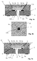
- an electronic device 1 is shown for MEMS devices according to a first embodiment which includes a substrate 2 , for example of the LGA/BGA type, having an upper surface 3 and a lower surface 4 opposed to the upper surface 3 , provided with an opening 5 passing between these surfaces 3 , 4 and including conductive tracks, at least partially interconnected with each other, formed on these surfaces 3 , 4 . Moreover, lands 4 a coupled to conductive tracks present on the lower surface 4 are present on this lower portion 4 .
- a MEMS device 6 including a die, for example of silicon, having a non active surface 7 and an active surface 8 opposed to the non active surface 7 .
- a sensitive portion 9 of MEMS device 6 is integrated.
- the MEMS device 6 is a sensor wherein the portion 9 is sensitive to chemical and/or physical variations of a fluid present outside the electronic device 1 , and the fluid interacts with the sensitive portion 9 of the MEMS device 6 , through the opening 5 .
- the active surface 8 of the MEMS device 6 faces the upper surface 3 of the substrate 2 and is spaced therefrom and the sensitive portion 9 is aligned to the opening 5 .
- peripheral portion of the active surface 8 of the MEMS device 6 is provided with connection lands for the electric connection to conductive tracks present on the upper surface 3 of the substrate 2 , by means of electric connections 10 , for example bumps.
- the MEMS device 6 is electrically mounted on the substrate 2 by means of known “flip-chip” assembly methods.
- a free central area 3 c aligned to the sensitive portion 9 a lateral area 3 a which surrounds the free central area 3 c wherein electric connections 10 are present which electrically couple the MEMS device 6 with the substrate 2
- the mean area 3 b surrounds the sensitive portion 9 of the MEMS device 6 .
- the electronic device 1 includes a protective package 11 , realized through molding, which incorporates the MEMS device 6 , the electric connections 10 and the substrate 2 , leaving the sensitive portion 9 of the MEMS device 6 and the lower surface 4 and the opening 5 of the substrate 2 exposed.
- the MEMS device 6 is enclosed in the protective package 11 .
- a barrier element 12 is positioned in an area 3 b which surrounds the sensitive portion 9 , i.e., it is realized in correspondence with the mean area 3 b.
- this barrier element 12 protects the sensitive portion 9 during the manufacturing step of the protective package 11 , through molding, so that this sensitive portion 9 remains free.
- the formation of the protective package 11 provides the introduction, inside a cavity of a mold, of the substrate 2 whereon the MEMS device 6 is mounted.
- an electrically insulating material at the melted state, which will be the plastic body of the protective package 11 .
- This material is typically a synthetic resin, for example, epoxy resin.
- the proper molding step involves the injection of the resin in the cavity of the mold. This step is then followed by a cooling step for completing the protective package 11 .
- the barrier element 12 is provided which completely surrounds at least the sensitive portion 9 of the MEMS device 6 .
- the barrier element 12 is a ring which completely surrounds the sensitive portion 9 of the MEMS device 6 , when the MEMS device 6 is mounted on the substrate 2 , and contacts the upper surface 3 of the substrate 2 and the active surface 8 .
- the barrier element 12 is formed by welding paste, therefore, in this embodiment, the electric connection step and the gluing step of the MEMS device 6 to the substrate 2 are carried out at the same time, resulting in a particularly compact structure of simple realization, not needing critical alignments between different structures.
- this barrier element 12 is completely coated by the protective package 11 .
- FIG. 2 Another embodiment of the device of FIG. 1 is shown with reference to FIG. 2 .
- a protective package 11 a realized through molding, incorporates the MEMS device 6 , the electric connections 10 and the substrate 2 , leave the sensitive portion 9 and the non active surface 7 of the MEMS device 6 , as well as the lower surface 4 and the opening 5 of the substrate 2 exposed.
- an electronic device 1 b according to a second embodiment is shown.
- the electronic device 1 b includes a substrate 2 , for example of the LGA/BGA type, having an upper surface 3 and a lower surface 4 opposed to the upper surface 3 , provided with an opening 5 .
- a MEMS device 6 includes a die, for example of silicon, having a non active surface 7 and an active surface 8 opposed to the non active surface 7 , wherein a sensitive portion 9 of a MEMS sensor is integrated.
- the active surface 8 of the MEMS device 6 faces the upper surface 3 of the substrate 2 and is spaced therefrom and the sensitive portion 9 is aligned to the opening 5 .
- peripheral portion of the active surface 8 of the MEMS device 6 is provided with connection lands for the electric connection to conductive tracks present on the upper surface 3 of the substrate 2 , by means of electric connections 10 , for example bumps.
- the MEMS device 6 is electrically mounted on the substrate 2 by means of the known “flip-chip” assembly methods.
- a free central area 3 c aligned to the sensitive portion 9
- a lateral area 3 a which surrounds the free central area 3 c wherein electric connections 10 are present which electrically couple the MEMS device 6 with the substrate 2
- a mean area 3 b included between the lateral area 3 a and the free central area 3 c.
- the electronic device /includes a protective package 11 b, realized through molding, which incorporates the MEMS device 6 , the electric connections 10 and the substrate 2 , leaving the sensitive portion 9 of the MEMS device 6 and the lower surface 4 and the opening 5 of the substrate 2 exposed.
- the MEMS device 6 is enclosed in the protective package 11 b.
- a barrier element 12 a, 12 b is positioned at least in an area 3 b which surrounds the sensitive portion 9 , i.e., it is realized at least in correspondence with the mean area 3 b.
- the barrier element 12 a is an irregular area 12 a formed on the upper surface 3 of the substrate 2 or the barrier element 12 b is an irregular area 12 b formed on the active surface 8 of the MEMS device 6 .
- this irregular area 12 a, 12 b shows a wrinkled surface.
- this irregular area 12 a extends on the upper surface 3 of the substrate 2 in correspondence with all the circuit free area 3 c.
- this irregular area 12 a is obtained by modifying the chemical properties of the upper surface 3 of the substrate 2 , as shown in FIG. 3 .
- the irregular area 12 a is formed by non wettable material.
- This layer 12 a of wettable material may be formed on the upper surface 3 of the substrate 2 .
- the barrier element 12 b is formed by an irregular area 12 b which is obtained by modifying the chemical properties of the active surface 8 of the MEMS device 6 .
- this irregular area 12 b extends on the active surface 8 of the MEMS device 6 in correspondence with the whole sensitive portion 9 of the MEMS device 6 .
- a protection layer 6 a including wettable material for example a plastic layer, for example including organic material such as Polyimide.
- the layer element of wettable material 6 a is removed leaving a dielectric layer 12 b of the non wettable type exposed, for example silicon oxide, which covers the sensitive portion 9 of the MEMS device 6 .
- the MEMS device 6 is welded on the substrate 2 and is subjected to a cleaning operation, for example in Plasma, by using a gas argon and oxygen mixture.
- the oxygen of the cleaning mixture chemically reacts with the layer 6 a of wettable material increasing its wettability, while the dielectric layer 12 b which covers the sensitive portion 9 is inert to the treatment.
- This difference of wettability implies a sudden slow down of the resin flow during the molding step of the protective package 11 b thereby the surface tension of the resin leads to the formation of a meniscus around the peripheral surface of the dielectric layer 12 b which covers the sensitive portion 9 .
- the peripheral surface of the dielectric layer 12 b is of circular shape.
- the barrier layer 12 b of non wettable material may be formed only on the active surface 8 of the upper MEMS device 3 of the substrate 2 of the sensitive portion 9 .
- the irregular area 12 a, 12 b shows some wrinkles.
- trenches are formed in the substrate or in the MEMS device 6 , so as to realize a preferred path defined in the substrate or on the MEMS device 6 for the resin during the molding step.
- these trenches completely surround the sensitive portion 9 of the MEMS device 6 .
- a layer of non wettable material can be present in correspondence with the sensitive portion 9 of the MEMS device 6 in the area surrounded by the trenches.
- this irregular area 12 a, 12 b protects the sensitive portion 9 during the manufacturing step of the protective package 11 a, through molding, having the liquid resin uniformly distributed around the electric connections without reaching the sensitive portion 9 .
- FIG. 4 An embodiment of the device of FIG. 3 is shown with reference to FIG. 4 .
- a protective package 11 c realized through molding, incorporates the MEMS device 6 , the electric connections 10 and the substrate 2 , leaving the sensitive portion 9 and the non active surface 7 of the MEMS device 6 , as well as the lower surface 4 and the opening 5 of the substrate 2 exposed.
- an electronic device 1 d according to a third embodiment is shown.
- an underfiller 13 is present in the lateral area 3 a so as to incorporate the electric connections 10 for mechanically strengthening the electronic device 1 in the connection area between the MEMS device 6 and the substrate 2 .
- the underfiller 13 is epoxy resin.
- the underfiller 13 shows a profile tapered outwards with respect of the lateral area 3 a on the opposite side with respect to the mean area 3 b, while it shows a substantially vertical profile in correspondence with the mean area 3 b.
- the cross section of the underfiller 13 increases when approaching the upper surface 3 of the substrate 2 .
- the electronic device 1 d also includes a protective package 11 d, realized through molding, which incorporates the MEMS device 6 , the underfiller 13 and the substrate 2 , leaving the sensitive portion 9 of the MEMS device 6 and the lower surface 4 and the opening 5 of the substrate 2 exposed.
- barrier material 12 allows maintaining the sensitive portion 9 of the MEMS device 6 , i.e., the central free area 3 c, free from the underfiller 13 .
- the underfiller 13 protects the active surface 8 of the MEMS device 6 during the manufacturing step of the plastic package 11 d.
- FIG. 5 An embodiment of the device of FIG. 5 is shown with reference to FIG. 6 .
- a protective package 11 e realized through molding, incorporates the MEMS device 6 , the underfiller 13 and the substrate 2 , leaving the sensitive portion 9 and the non active surface 7 of the MEMS device 6 , as well as the lower surface 4 and the opening 5 of the substrate 2 exposed.
- an underfiller 13 is present in the lateral area 3 a so as to incorporate the electric connections 10 to mechanically strengthen the electronic device 1 in the connection area between the MEMS device 6 and the substrate 2 .
- the underfiller 13 shows a tapered profile outside the lateral area 3 a on the opposite side with respect to the mean area 3 b, while it shows a substantially vertical profile in correspondence with the mean area 3 b.
- the cross section of the underfiller 13 increases when approaching the upper surface 3 of the substrate 2 .
- the electronic device if also includes a protective package 11 f, realized through molding, which incorporates the MEMS device 6 , the underfiller 13 and the substrate 2 , leaving the sensitive portion 9 of the MEMS device 6 and the lower surface 4 and the opening 5 of the substrate 2 exposed.
- a protective package 11 f realized through molding, which incorporates the MEMS device 6 , the underfiller 13 and the substrate 2 , leaving the sensitive portion 9 of the MEMS device 6 and the lower surface 4 and the opening 5 of the substrate 2 exposed.
- barrier element 12 a allows maintaining the sensitive portion 9 of the MEMS device 6 free from the underfiller 13 .
- FIG. 7 a A further embodiment of the device of FIG. 7 is shown with reference to FIG. 7 a.
- the barrier element 12 b is formed on the active surface 8 of the MEMS device 6 around the sensitive portion 9 , prior to the formation of the underfiller 13 , with the same modes with which the barrier element 12 b of FIG. 3 a is realized.
- the difference of wettability between the barrier element 12 b and the portion outside the barrier layer implies a sudden slow down of the flow of the underfiller 13 during its dispensing step after the MEMS device 6 has been fixed to the substrate, thereby the surface tension of the underfiller 13 leads to the formation of a meniscus around the peripheral surface of the barrier element 12 b which at least surrounds the sensitive portion 9 .
- FIG. 7 An embodiment of the device of FIG. 7 is shown with reference to FIG. 8 .
- a protective package 11 g realized through molding, incorporates the MEMS device 6 , the underfiller 13 and the substrate 2 , leaving the sensitive portion 9 and the non active surface 7 of the MEMS device 6 , as well as the lower surface 4 and the opening 5 of the substrate 2 exposed.
- an underfiller 13 is present in the lateral area 3 a so as to incorporate the electric connections 10 to mechanically strengthen the electronic device 1 in the connection area between the MEMS device 6 and the substrate 2 .
- FIGS. 9 and 10 two further versions of an electronic device 1 h according to the first embodiment are shown.
- the electronic device 1 h includes an integrated circuit 14 having a first surface 14 a and a second surface 14 b opposed to the first surface, the integrated circuit 14 being mounted with the first surface 14 a on the non active surface 7 of the MEMS device 6 .
- the integrated circuit 14 is thus electrically coupled to the conductive tracks present on the upper surface 3 of the substrate 2 by means of further electric connections 15 .
- the dimension of the cross section of this integrated circuit 14 is greater than the dimension of the cross section of the MEMS device 6 .
- a passivated circuitry is integrated and moreover the first surface 14 a is provided with connection lands for the electric connection to the MEMS device 6 , by means of bumps.
- a passivated circuitry is integrated and moreover connection lands are provided for the electric connection to the MEMS device 6 through wire-bonding.
- a protective package 11 h realized through molding, incorporates the MEMS device 6 , the integrated circuit 14 , the connections 15 and the substrate 2 , leaving the sensitive portion 9 and the non active surface 7 of the MEMS device 6 , as well as the lower surface 4 and the opening 5 of the substrate 2 exposed.
- FIGS. 11 and 12 two further versions are shown of an electronic device 1 g according to the third embodiment.
- the electronic device 1 g includes an integrated circuit 14 having a first surface 14 a and a second surface 14 b opposed to the first surface, which is mounted with the first surface 14 a on the non active surface 7 of the MEMS device 6 .
- the integrated device 14 is then electrically coupled to the conductive tracks formed on the upper surface 3 of the substrate 2 by means of further electric connections 15 .
- the dimension of the cross section of this integrated circuit 14 is greater than the dimension of the cross section of the MEMS device 6 .
- the underfiller 13 is also present in an area 14 c included between a portion of the first surface 14 a projecting with respect to the MEMS device and the upper surface 3 of the substrate 2 .
- the underfiller 13 shows a tapered profile outside the area 14 c.
- the cross section of the underfiller 13 increases when approaching the upper surface 3 of the substrate 2 .
- the first surface 14 a is provided with connection lands for the electric connection to the MEMS device 6 , by means of bump (flip-chip) bonding.
- connection lands for the electric connection to the MEMS device 6 , by means of connection wires (wirebonding).
- a protective package 11 g realized through molding, incorporates the MEMS device 6 , the integrated circuit 14 , the connections 15 , the underfiller 13 and the substrate 2 , leaving the sensitive portion 9 and the non active surface 7 of the MEMS device 6 , as well as the lower surface 4 and the opening 5 of the substrate 2 exposed.
- underfiller 13 allows the protection of both the integrated circuit 14 and the MEMS device 6 during the molding step of the protective package 11 g.
- the electronic device 1 i is shown which is a further version of the electronic device of FIG. 9 , wherein the protective package 11 i leaves the second surface 14 b of the integrated circuit 14 exposed.
- the electronic device 1 l is shown which is a further embodiment of the electronic device of FIG. 11 , wherein the protective package 11 l leaves the second surface 14 b of the integrated circuit 14 exposed.
- the device 1 of FIG. 1 is shown wherein an integrated circuit 16 is mounted on the substrate 2 flanked by the MEMS device 6 , and fixed to the substrate 2 , for example by means of a welding layer 16 b.
- the integrated circuit 16 is electrically coupled to the substrate 2 by means of further electric connections 16 a.
- the protective package 11 realized through molding, incorporates the MEMS device 6 with the electric connections 10 , the integrated circuit 16 with the electric connections 16 a and the substrate 2 , leaving the sensitive portion 9 of the MEMS device 6 , as well as the lower surface 4 and the opening 5 of the substrate 2 exposed.
- the device 1 d of FIG. 5 is shown wherein an integrated circuit 16 is mounted on the substrate 2 flanked to the MEMS device 6 , and fixed to the substrate 2 , for example by means of a welding layer 16 b.
- the integrated circuit 16 is electrically coupled to the substrate 2 by means of further electric connections 16 a.
- the protective package 11 d realized through molding, incorporates the MEMS device 6 , the underfiller 13 , the integrated circuit 16 with the further electric connections 16 a and the substrate 2 , leaving sensitive portion 9 of the MEMS device 6 , as well as the lower surface 4 and the opening 5 of the substrate 2 exposed.
- the device 1 a of FIG. 2 is shown wherein an integrated circuit 16 is mounted on the substrate 2 flanked to the device MEMS 6 , and fixed to the substrate 2 , for example by means of a welding layer 16 b.
- the integrated circuit 16 is electrically coupled to the substrate 2 by means of further electric connections 16 a.
- the protective package 11 a realized through molding, incorporates the MEMS device 6 with the electric connections 10 , the integrated circuit 16 with the further electric connections 16 a and the substrate 2 , leaving the sensitive portion 9 and the non active surface 7 of the MEMS device 6 , as well as the lower surface 4 and the opening 5 of the substrate 2 exposed.
- the device 1 e of FIG. 6 is shown wherein an integrated circuit 16 is mounted on the substrate 2 flanked to the MEMS device 6 , and fixed to the substrate 2 , for example by means of a welding layer 16 b.
- the integrated circuit 16 is electrically coupled to the substrate 2 by means of further electric connections 16 a.
- the protective package 11 e realized through molding, incorporates the MEMS device 6 , the underfiller 13 , the integrated circuit 16 with the further electric connections 16 a and the substrate 2 , leaving the sensitive portion 9 and the non active surface 7 of the MEMS device 6 , as well as the lower surface 4 and the opening 5 of the substrate 2 exposed.
- the device 1 h of FIG. 9 is shown wherein a second integrated circuit 16 is mounted on the substrate 2 flanked to the MEMS device 6 , and fixed to the substrate 2 , for example by means of a welding layer 16 b.
- the second integrated circuit 16 is electrically coupled to the substrate 2 by means of further electric connections 16 a.
- a third integrated circuit 17 is mounted on the second surface 14 b of the integrated circuit 14 , and electrically coupled to the substrate 2 by means of further electric connections 17 a.
- a fourth integrated circuit 18 is mounted on the second integrated circuit 16 and electrically coupled to the substrate 2 by means of further electric connections 18 a.
- the protective package 11 h realized through molding, incorporates the MEMS device 6 , the electric connections 10 , the integrated circuits 14 , 16 , 17 and 18 with the relative electric connections 15 , 16 a, 17 a and 18 a and the substrate 2 , leaving the sensitive portion 9 of the MEMS device 6 , as well as the lower surface 4 and the opening 5 of the substrate 2 exposed.
- the device 1 g of FIG. 11 is shown wherein a second integrated circuit 16 is mounted on the substrate 2 flanked to the MEMS device 6 , and fixed to the substrate 2 , for example by means of a welding layer 16 b.
- the second integrated circuit 16 is electrically coupled to the substrate 2 by means of further electric connections 16 a.
- a third integrated circuit 17 is mounted on the second surface 14 b of the integrated circuit 14 , and electrically coupled to the substrate 2 by means of further electric connections 17 a.
- a fourth integrated circuit 18 is mounted on the second integrated circuit 16 and electrically coupled to the substrate 2 by means of further electric connections 18 a.
- the protective package 11 g realized through molding, incorporates the MEMS device 6 , the underfiller 13 , the integrated circuits 14 , 16 , 17 and 18 with the relative electric connections 15 , 16 a, 17 a and 18 a and the substrate 2 , leaving the sensitive portion 9 of the MEMS device 6 , as well as the lower surface 4 and the opening 5 of the substrate 2 exposed.
- the integrated circuits 14 , 16 , 17 and 18 can be sensor devices, for example accelerometers 14 , gyroscopes 18 , magnetometers 17 to form an IMU (inertial measurement unit).
- IMU inertial measurement unit
- microphones pressure, gas, chemical sensors
- a protective package realized by means of molding.
- These devices can, in turn, be contained in a variety of different types of electronic systems, such as barometric systems, audio systems, computer systems, control systems, safety systems, and so on.
- the electronic device as a whole shows an overall dimension included between 3 ⁇ 3 ⁇ 1 mm ⁇ 3, while the MEMS device 6 has a width of 1500 ⁇ m a length of 1500 ⁇ m and a thickness of 700 ⁇ m.
- the sensitive portion 9 of the MEMS device 6 has a diameter included between 100 ⁇ m and 1000 ⁇ m.
- the distance between the active surface 8 of the MEMS device 6 and the upper surface 3 of the substrate is included between 50 and 500 ⁇ m, while the thickness of the substrate is included between about 150 and 300 ⁇ m and the width of the opening 5 is included between 100 and 700 ⁇ m.
- barrier element 12 is realized with a ring of welding paste it has a thickness of a cross section included between 60 and 300 ⁇ m.
- the barrier element 12 a, 12 b is realized with an irregular area it has a width of a cross section of about 10-50 ⁇ m and, for example, a depth included between 20-80 ⁇ m.
- electronic devices according to embodiments are particularly compact and use technical solutions which do not provide critical alignments.
- the presence of the barrier element 12 , 12 a allows protecting the sensitive portion 9 of the MEMS device 6 during the manufacturing steps of the protective package 11 or during the dispensing step of the underfiller 13 in the electronic device 1 .
- this barrier element 12 , 12 a, 12 b can be of physical or chemical nature or a combination of the two.
- barrier elements 12 , 12 a, 12 b can be realized both on the substrate 2 and on the MEMS device 6 .
Abstract
An electronic device includes a substrate provided with a passing opening and a MEMS device including an active surface wherein a portion of the MEMS device is integrated sensitive to chemical/physical variations of a fluid. The active surface of the MEMS device faces the substrate and is spaced therefrom, the sensitive portion being aligned to the opening. A protective package incorporates at least partially the MEMS device and the substrate, leaving at least the sensitive portion of the MEMS device, and the opening of the substrate exposed. A barrier element is positioned in an area which surrounds the sensitive portion to realize a protection structure for the MEMS device, so that the sensitive portion is free.
Description
The present application is a divisional of U.S. patent application Ser. No. 12/006,819, filed Jan. 4, 2008, which application claims priority from Italian patent application No. MI2007A 000008, filed Jan. 4, 2007, and Italian patent application No. MI2007A 000007, filed Jan. 4, 2007; all the foregoing applications are incorporated herein by reference in their entireties.
Embodiments of the present disclosure relate generally to an electronic device including MEMS devices and holed substrates, in particular of the LGA or BGA type.
More specifically, embodiments of the present disclosure relate particularly, but not exclusively, to an electronic device including MEMS sensors mounted on an LGA substrate, wherein the MEMS sensor needs a physical interface of communication with the outer environment of the electronic device and the following description is made with reference to this field of application for convenience of illustration only.
As it is well known, a MEMS device (micro-electro-mechanical system) is a micro device which integrated the mechanical and electrical functions in a silicon chip or die realized by using the lithographic techniques of micro manufacturing. The final assembled device is typically made of the silicon die wherein the MEMS is integrated and, optionally, of integrated circuits for specific applications mounted on a substrate, for example, of the LGA or BGA type (Land Grid Array or Ball Grid Array), flanked or piled onto the MEMS device, using the conventional assembling processes.
A cover or cap fixed to the substrate, encapsulates the MEMS device and the other integrated circuits mounted on the substrate, forming the package for protecting it from external physical stresses.
If the MEMS device is a pressure, gas or liquid sensor or a microphone, the cover is provided with holes for allowing the interaction between the device and outside of the assembled device.
It is also known that the substrate of the LGA/BGA type is formed by conductive layers insulated from each other by means of layers of insulating or dielectric material. The conductive layers are shaped in conductive tracks insulated from each other by layers of insulating or dielectric material. Conductive holes, called “vias”, are typically realized through the insulating layers with a vertical orientation with respect to the layers, to form conductive paths between conductive tracks belonging to different conductive layers.
The MEMS devices are then electrically coupled to the outside of the final device, through wires which connect contact lands provided on the MEMS devices with the conductive tracks present on the substrate inside the cover.
Although advantageous under several aspects, these types of assembled electronic devices including MEMS sensors require, between the cap/cover and the substrate, a welding ring.
Moreover, the formation of this cover/cap which completes the assembled electronic device provides a series of process steps which are not provided in the realization of integrated circuits, with a considerable cost increase.
There is a need for electronic devices including MEMS devices and having such structural characteristics as to allow this electronic device to be made with manufacturing processes of conventional integrated circuits, overcoming the limits and/or the drawbacks still limiting the electronic devices realized according to the prior art.
Embodiments of the present disclosure are directed to an electronic device including a MEMS device wherein the protective package is realized by means of molding.
According to one embodiment, an electronic device includes a substrate provided with a passing opening and a MEMS device including an active surface wherein a portion of the MEMS device is integrated sensitive to chemical/physical variations of a fluid. The active surface of the MEMS device faces the substrate and is spaced therefrom, the sensitive portion being aligned to the opening. A protective package, which incorporates at least partially the MEMS device and the substrate, leaves at least the sensitive portion of the MEMS device and the opening of the substrate exposed. A barrier element is positioned in an area which surrounds the sensitive portion for realizing a protection structure for the MEMS device, so that the sensitive portion is free.
The characteristics and the advantages of electronic devices and methods of forming such devices according to the present disclosure will be apparent from the following description of embodiments thereof given by way of indicative and non limiting example with reference to the annexed drawings.
In these figures:
The following discussion is presented to enable a person skilled in the art to make and use the subject matter disclosed herein. Various modifications to the embodiments will be readily apparent to those skilled in the art, and the generic principles herein may be applied to other embodiments and applications without departing from the spirit and scope of the present subject matter. Thus, the present disclosure is not intended to be limited to the embodiments shown, but is to be accorded the widest scope consistent with the principles and features disclosed herein.
With reference to FIG. 1 , an electronic device 1 is shown for MEMS devices according to a first embodiment which includes a substrate 2, for example of the LGA/BGA type, having an upper surface 3 and a lower surface 4 opposed to the upper surface 3, provided with an opening 5 passing between these surfaces 3, 4 and including conductive tracks, at least partially interconnected with each other, formed on these surfaces 3, 4. Moreover, lands 4 a coupled to conductive tracks present on the lower surface 4 are present on this lower portion 4. A MEMS device 6 including a die, for example of silicon, having a non active surface 7 and an active surface 8 opposed to the non active surface 7. Advantageously, in the silicon die, in correspondence with the active surface 8, a sensitive portion 9 of MEMS device 6 is integrated. In particular, the MEMS device 6 is a sensor wherein the portion 9 is sensitive to chemical and/or physical variations of a fluid present outside the electronic device 1, and the fluid interacts with the sensitive portion 9 of the MEMS device 6, through the opening 5.
According to this embodiment the active surface 8 of the MEMS device 6 faces the upper surface 3 of the substrate 2 and is spaced therefrom and the sensitive portion 9 is aligned to the opening 5.
Moreover, the peripheral portion of the active surface 8 of the MEMS device 6 is provided with connection lands for the electric connection to conductive tracks present on the upper surface 3 of the substrate 2, by means of electric connections 10, for example bumps.
Advantageously, the MEMS device 6 is electrically mounted on the substrate 2 by means of known “flip-chip” assembly methods.
In particular, between the active surface 8 of the MEMS device 6 and the upper surface 3 of the substrate 2 different functional areas remain defined: a free central area 3 c aligned to the sensitive portion 9, a lateral area 3 a which surrounds the free central area 3 c wherein electric connections 10 are present which electrically couple the MEMS device 6 with the substrate 2, and a mean area 3 b included between the lateral area 3 a and the free central area 3 c. In particular also the mean area 3 b surrounds the sensitive portion 9 of the MEMS device 6.
Also according to embodiments, the electronic device 1 includes a protective package 11, realized through molding, which incorporates the MEMS device 6, the electric connections 10 and the substrate 2, leaving the sensitive portion 9 of the MEMS device 6 and the lower surface 4 and the opening 5 of the substrate 2 exposed.
In other words, the MEMS device 6 is enclosed in the protective package 11.
According to embodiments, a barrier element 12 is positioned in an area 3 b which surrounds the sensitive portion 9, i.e., it is realized in correspondence with the mean area 3 b.
Advantageously according to embodiments, the presence of this barrier element 12 protects the sensitive portion 9 during the manufacturing step of the protective package 11, through molding, so that this sensitive portion 9 remains free.
In particular, in a known way, the formation of the protective package 11 provides the introduction, inside a cavity of a mold, of the substrate 2 whereon the MEMS device 6 is mounted.
In the mold cavity the injection under pressure and at high temperature is then provided of an electrically insulating material at the melted state, which will be the plastic body of the protective package 11. This material is typically a synthetic resin, for example, epoxy resin.
The proper molding step involves the injection of the resin in the cavity of the mold. This step is then followed by a cooling step for completing the protective package 11.
For avoiding damage by the resin of the sensitive portion 9 of the MEMS device 6 during the resin injection step, according to embodiments, between the upper surface 3 of the substrate 2 and the active surface 8, the barrier element 12 is provided which completely surrounds at least the sensitive portion 9 of the MEMS device 6.
Advantageously, the barrier element 12 is a ring which completely surrounds the sensitive portion 9 of the MEMS device 6, when the MEMS device 6 is mounted on the substrate 2, and contacts the upper surface 3 of the substrate 2 and the active surface 8.
Advantageously, the barrier element 12 is formed by welding paste, therefore, in this embodiment, the electric connection step and the gluing step of the MEMS device 6 to the substrate 2 are carried out at the same time, resulting in a particularly compact structure of simple realization, not needing critical alignments between different structures.
In this first embodiment the outer edge of this barrier element 12 is completely coated by the protective package 11.
Another embodiment of the device of FIG. 1 is shown with reference to FIG. 2 .
Elements being structurally and functionally identical with respect to the device described with reference to FIG. 1 will be given the same reference numbers.
In particular, in this electronic device 1 a, a protective package 11 a, realized through molding, incorporates the MEMS device 6, the electric connections 10 and the substrate 2, leave the sensitive portion 9 and the non active surface 7 of the MEMS device 6, as well as the lower surface 4 and the opening 5 of the substrate 2 exposed.
With reference to FIGS. 3 , 3 a and 3 b, an electronic device 1 b according to a second embodiment is shown.
Elements being structurally and functionally identical with respect to the device described with reference to FIG. 1 will be given the same reference numbers.
In particular, the electronic device 1 b includes a substrate 2, for example of the LGA/BGA type, having an upper surface 3 and a lower surface 4 opposed to the upper surface 3, provided with an opening 5. A MEMS device 6 includes a die, for example of silicon, having a non active surface 7 and an active surface 8 opposed to the non active surface 7, wherein a sensitive portion 9 of a MEMS sensor is integrated.
According to this embodiment the active surface 8 of the MEMS device 6 faces the upper surface 3 of the substrate 2 and is spaced therefrom and the sensitive portion 9 is aligned to the opening 5.
Moreover, the peripheral portion of the active surface 8 of the MEMS device 6 is provided with connection lands for the electric connection to conductive tracks present on the upper surface 3 of the substrate 2, by means of electric connections 10, for example bumps.
Advantageously, the MEMS device 6 is electrically mounted on the substrate 2 by means of the known “flip-chip” assembly methods.
Therefore, between the active surface 8 of the MEMS device 6 and the upper surface 3 of the substrate 2 three areas are identified: a free central area 3 c aligned to the sensitive portion 9, a lateral area 3 a which surrounds the free central area 3 c wherein electric connections 10 are present which electrically couple the MEMS device 6 with the substrate 2, and a mean area 3 b included between the lateral area 3 a and the free central area 3 c.
Also according to this embodiment, the electronic device/includes a protective package 11 b, realized through molding, which incorporates the MEMS device 6, the electric connections 10 and the substrate 2, leaving the sensitive portion 9 of the MEMS device 6 and the lower surface 4 and the opening 5 of the substrate 2 exposed.
In other words, the MEMS device 6 is enclosed in the protective package 11 b.
According to this embodiment, a barrier element 12 a, 12 b is positioned at least in an area 3 b which surrounds the sensitive portion 9, i.e., it is realized at least in correspondence with the mean area 3 b.
In this second embodiment, the barrier element 12 a is an irregular area 12 a formed on the upper surface 3 of the substrate 2 or the barrier element 12 b is an irregular area 12 b formed on the active surface 8 of the MEMS device 6.
Advantageously, this irregular area 12 a, 12 b shows a wrinkled surface.
Advantageously, this irregular area 12 a extends on the upper surface 3 of the substrate 2 in correspondence with all the circuit free area 3 c.
Advantageously, according to this embodiment this irregular area 12 a is obtained by modifying the chemical properties of the upper surface 3 of the substrate 2, as shown in FIG. 3 .
Advantageously, the irregular area 12 a is formed by non wettable material.
This layer 12 a of wettable material may be formed on the upper surface 3 of the substrate 2.
As shown in FIGS. 3 a and 3 b, advantageously according to this embodiment the barrier element 12 b is formed by an irregular area 12 b which is obtained by modifying the chemical properties of the active surface 8 of the MEMS device 6.
Advantageously, this irregular area 12 b extends on the active surface 8 of the MEMS device 6 in correspondence with the whole sensitive portion 9 of the MEMS device 6.
It is in fact known that the active surface 8 of the MEMS device 6 is covered by a protection layer 6 a including wettable material, for example a plastic layer, for example including organic material such as Polyimide.
According to this embodiment, from the sensitive portion 9 of the MEMS device 6 the layer element of wettable material 6 a is removed leaving a dielectric layer 12 b of the non wettable type exposed, for example silicon oxide, which covers the sensitive portion 9 of the MEMS device 6.
Advantageously, after the removal step from the sensitive portion 9 of the MEMS device 6 of the layer 6 a of wettable material, the MEMS device 6 is welded on the substrate 2 and is subjected to a cleaning operation, for example in Plasma, by using a gas argon and oxygen mixture.
Advantageously, the oxygen of the cleaning mixture chemically reacts with the layer 6 a of wettable material increasing its wettability, while the dielectric layer 12 b which covers the sensitive portion 9 is inert to the treatment.
Therefore, as a result after the treatment an increased wettability of the layer 6 a of wettable material is obtained, comparable to that of the upper surface 3 of the substrate 2 and a reduced wettability of the surface of the dielectric layer 12 b which covers the sensitive portion 9.
This difference of wettability implies a sudden slow down of the resin flow during the molding step of the protective package 11 b thereby the surface tension of the resin leads to the formation of a meniscus around the peripheral surface of the dielectric layer 12 b which covers the sensitive portion 9.
Advantageously, as shown in FIG. 3 b, the peripheral surface of the dielectric layer 12 b is of circular shape.
The barrier layer 12 b of non wettable material may be formed only on the active surface 8 of the upper MEMS device 3 of the substrate 2 of the sensitive portion 9.
In a further version of this second embodiment the irregular area 12 a, 12 b shows some wrinkles.
Advantageously, in the irregular area 12 a, 12 b trenches are formed in the substrate or in the MEMS device 6, so as to realize a preferred path defined in the substrate or on the MEMS device 6 for the resin during the molding step.
Advantageously, these trenches completely surround the sensitive portion 9 of the MEMS device 6.
Advantageously, in this latter embodiment a layer of non wettable material can be present in correspondence with the sensitive portion 9 of the MEMS device 6 in the area surrounded by the trenches.
According to this embodiment, the presence of this irregular area 12 a, 12 b protects the sensitive portion 9 during the manufacturing step of the protective package 11 a, through molding, having the liquid resin uniformly distributed around the electric connections without reaching the sensitive portion 9.
An embodiment of the device of FIG. 3 is shown with reference to FIG. 4 .
Elements being structurally and functionally identical with respect to the device described with reference to FIG. 3 will be given the same reference numbers.
In particular, in this electronic device 1 c, a protective package 11 c, realized through molding, incorporates the MEMS device 6, the electric connections 10 and the substrate 2, leaving the sensitive portion 9 and the non active surface 7 of the MEMS device 6, as well as the lower surface 4 and the opening 5 of the substrate 2 exposed.
With reference to FIG. 5 , an electronic device 1 d according to a third embodiment is shown.
Elements being structurally and functionally identical with respect to the device described with reference to FIG. 1 will be given the same reference numbers.
In particular, in this embodiment an underfiller 13 is present in the lateral area 3 a so as to incorporate the electric connections 10 for mechanically strengthening the electronic device 1 in the connection area between the MEMS device 6 and the substrate 2.
Advantageously, the underfiller 13 is epoxy resin.
Advantageously, the underfiller 13 shows a profile tapered outwards with respect of the lateral area 3 a on the opposite side with respect to the mean area 3 b, while it shows a substantially vertical profile in correspondence with the mean area 3 b.
In other words, the cross section of the underfiller 13 increases when approaching the upper surface 3 of the substrate 2.
The electronic device 1 d also includes a protective package 11 d, realized through molding, which incorporates the MEMS device 6, the underfiller 13 and the substrate 2, leaving the sensitive portion 9 of the MEMS device 6 and the lower surface 4 and the opening 5 of the substrate 2 exposed.
The presence of the barrier material 12 allows maintaining the sensitive portion 9 of the MEMS device 6, i.e., the central free area 3 c, free from the underfiller 13.
Moreover, the underfiller 13 protects the active surface 8 of the MEMS device 6 during the manufacturing step of the plastic package 11 d.
An embodiment of the device of FIG. 5 is shown with reference to FIG. 6 .
Elements being structurally and functionally identical with respect to the device described with reference to FIG. 5 will be given the same reference numbers.
In particular, in this electronic device 1 e, a protective package 11 e, realized through molding, incorporates the MEMS device 6, the underfiller 13 and the substrate 2, leaving the sensitive portion 9 and the non active surface 7 of the MEMS device 6, as well as the lower surface 4 and the opening 5 of the substrate 2 exposed.
With reference to FIG. 7 , an electronic device if according to a fourth embodiment is shown.
Elements being structurally and functionally identical with respect to the device described with reference to FIG. 3 will be given the same reference numbers.
In particular, in this embodiment an underfiller 13 is present in the lateral area 3 a so as to incorporate the electric connections 10 to mechanically strengthen the electronic device 1 in the connection area between the MEMS device 6 and the substrate 2.
Advantageously, the underfiller 13 shows a tapered profile outside the lateral area 3 a on the opposite side with respect to the mean area 3 b, while it shows a substantially vertical profile in correspondence with the mean area 3 b.
In other words, the cross section of the underfiller 13 increases when approaching the upper surface 3 of the substrate 2.
The electronic device if also includes a protective package 11 f, realized through molding, which incorporates the MEMS device 6, the underfiller 13 and the substrate 2, leaving the sensitive portion 9 of the MEMS device 6 and the lower surface 4 and the opening 5 of the substrate 2 exposed.
The presence of the barrier element 12 a allows maintaining the sensitive portion 9 of the MEMS device 6 free from the underfiller 13.
A further embodiment of the device of FIG. 7 is shown with reference to FIG. 7 a.
Elements being structurally and functionally identical with respect to the device described with reference to FIG. 7 will be given the same reference numbers.
In this embodiment the barrier element 12 b is formed on the active surface 8 of the MEMS device 6 around the sensitive portion 9, prior to the formation of the underfiller 13, with the same modes with which the barrier element 12 b of FIG. 3 a is realized.
In particular, the difference of wettability between the barrier element 12 b and the portion outside the barrier layer implies a sudden slow down of the flow of the underfiller 13 during its dispensing step after the MEMS device 6 has been fixed to the substrate, thereby the surface tension of the underfiller 13 leads to the formation of a meniscus around the peripheral surface of the barrier element 12 b which at least surrounds the sensitive portion 9.
An embodiment of the device of FIG. 7 is shown with reference to FIG. 8 .
Elements being structurally and functionally identical with respect to the device described with reference to FIG. 7 will be given the same reference numbers.
In particular, in this electronic device 1 g, a protective package 11 g, realized through molding, incorporates the MEMS device 6, the underfiller 13 and the substrate 2, leaving the sensitive portion 9 and the non active surface 7 of the MEMS device 6, as well as the lower surface 4 and the opening 5 of the substrate 2 exposed.
In particular, in this embodiment an underfiller 13 is present in the lateral area 3 a so as to incorporate the electric connections 10 to mechanically strengthen the electronic device 1 in the connection area between the MEMS device 6 and the substrate 2.
With reference to FIGS. 9 and 10 , two further versions of an electronic device 1 h according to the first embodiment are shown.
Elements being structurally and functionally identical with respect to the device described with reference to FIG. 1 will be given the same reference numbers.
In particular, the electronic device 1 h includes an integrated circuit 14 having a first surface 14 a and a second surface 14 b opposed to the first surface, the integrated circuit 14 being mounted with the first surface 14 a on the non active surface 7 of the MEMS device 6.
The integrated circuit 14 is thus electrically coupled to the conductive tracks present on the upper surface 3 of the substrate 2 by means of further electric connections 15.
For example, the dimension of the cross section of this integrated circuit 14 is greater than the dimension of the cross section of the MEMS device 6.
Advantageously, as shown in FIG. 9 , on the first surface 14 a a passivated circuitry is integrated and moreover the first surface 14 a is provided with connection lands for the electric connection to the MEMS device 6, by means of bumps.
Advantageously, as shown in FIG. 10 , on the second surface 14 b a passivated circuitry is integrated and moreover connection lands are provided for the electric connection to the MEMS device 6 through wire-bonding.
A protective package 11 h, realized through molding, incorporates the MEMS device 6, the integrated circuit 14, the connections 15 and the substrate 2, leaving the sensitive portion 9 and the non active surface 7 of the MEMS device 6, as well as the lower surface 4 and the opening 5 of the substrate 2 exposed.
With reference to FIGS. 11 and 12 , two further versions are shown of an electronic device 1 g according to the third embodiment.
Elements being structurally and functionally identical with respect to the device described with reference to FIG. 5 will be given the same reference numbers.
In particular, the electronic device 1 g includes an integrated circuit 14 having a first surface 14 a and a second surface 14 b opposed to the first surface, which is mounted with the first surface 14 a on the non active surface 7 of the MEMS device 6.
The integrated device 14 is then electrically coupled to the conductive tracks formed on the upper surface 3 of the substrate 2 by means of further electric connections 15.
Advantageously, the dimension of the cross section of this integrated circuit 14 is greater than the dimension of the cross section of the MEMS device 6.
Advantageously, the underfiller 13 is also present in an area 14 c included between a portion of the first surface 14 a projecting with respect to the MEMS device and the upper surface 3 of the substrate 2.
Advantageously, the underfiller 13 shows a tapered profile outside the area 14 c.
In other words the cross section of the underfiller 13 increases when approaching the upper surface 3 of the substrate 2.
Advantageously, as shown in FIG. 11 , the first surface 14 a is provided with connection lands for the electric connection to the MEMS device 6, by means of bump (flip-chip) bonding.
Advantageously, as shown in FIG. 12 , the second surface 14 b is provided with connection lands for the electric connection to the MEMS device 6, by means of connection wires (wirebonding).
A protective package 11 g, realized through molding, incorporates the MEMS device 6, the integrated circuit 14, the connections 15, the underfiller 13 and the substrate 2, leaving the sensitive portion 9 and the non active surface 7 of the MEMS device 6, as well as the lower surface 4 and the opening 5 of the substrate 2 exposed.
The presence of the underfiller 13 allows the protection of both the integrated circuit 14 and the MEMS device 6 during the molding step of the protective package 11 g.
With reference to FIG. 13 the electronic device 1 i is shown which is a further version of the electronic device of FIG. 9 , wherein the protective package 11 i leaves the second surface 14 b of the integrated circuit 14 exposed.
With reference to FIG. 14 the electronic device 1 l is shown which is a further embodiment of the electronic device of FIG. 11 , wherein the protective package 11 l leaves the second surface 14 b of the integrated circuit 14 exposed.
With reference to FIG. 15 , the device 1 of FIG. 1 is shown wherein an integrated circuit 16 is mounted on the substrate 2 flanked by the MEMS device 6, and fixed to the substrate 2, for example by means of a welding layer 16 b.
The integrated circuit 16 is electrically coupled to the substrate 2 by means of further electric connections 16 a.
The protective package 11, realized through molding, incorporates the MEMS device 6 with the electric connections 10, the integrated circuit 16 with the electric connections 16 a and the substrate 2, leaving the sensitive portion 9 of the MEMS device 6, as well as the lower surface 4 and the opening 5 of the substrate 2 exposed.
With reference to FIG. 16 , the device 1 d of FIG. 5 is shown wherein an integrated circuit 16 is mounted on the substrate 2 flanked to the MEMS device 6, and fixed to the substrate 2, for example by means of a welding layer 16 b.
The integrated circuit 16 is electrically coupled to the substrate 2 by means of further electric connections 16 a.
The protective package 11 d, realized through molding, incorporates the MEMS device 6, the underfiller 13, the integrated circuit 16 with the further electric connections 16 a and the substrate 2, leaving sensitive portion 9 of the MEMS device 6, as well as the lower surface 4 and the opening 5 of the substrate 2 exposed.
With reference to FIG. 17 , the device 1 a of FIG. 2 is shown wherein an integrated circuit 16 is mounted on the substrate 2 flanked to the device MEMS 6, and fixed to the substrate 2, for example by means of a welding layer 16 b.
The integrated circuit 16 is electrically coupled to the substrate 2 by means of further electric connections 16 a.
The protective package 11 a, realized through molding, incorporates the MEMS device 6 with the electric connections 10, the integrated circuit 16 with the further electric connections 16 a and the substrate 2, leaving the sensitive portion 9 and the non active surface 7 of the MEMS device 6, as well as the lower surface 4 and the opening 5 of the substrate 2 exposed.
With reference to FIG. 18 , the device 1 e of FIG. 6 is shown wherein an integrated circuit 16 is mounted on the substrate 2 flanked to the MEMS device 6, and fixed to the substrate 2, for example by means of a welding layer 16 b.
The integrated circuit 16 is electrically coupled to the substrate 2 by means of further electric connections 16 a.
The protective package 11 e, realized through molding, incorporates the MEMS device 6, the underfiller 13, the integrated circuit 16 with the further electric connections 16 a and the substrate 2, leaving the sensitive portion 9 and the non active surface 7 of the MEMS device 6, as well as the lower surface 4 and the opening 5 of the substrate 2 exposed.
With reference to FIG. 19 , the device 1 h of FIG. 9 is shown wherein a second integrated circuit 16 is mounted on the substrate 2 flanked to the MEMS device 6, and fixed to the substrate 2, for example by means of a welding layer 16 b.
The second integrated circuit 16 is electrically coupled to the substrate 2 by means of further electric connections 16 a.
A third integrated circuit 17 is mounted on the second surface 14 b of the integrated circuit 14, and electrically coupled to the substrate 2 by means of further electric connections 17 a.
A fourth integrated circuit 18 is mounted on the second integrated circuit 16 and electrically coupled to the substrate 2 by means of further electric connections 18 a.
The protective package 11 h, realized through molding, incorporates the MEMS device 6, the electric connections 10, the integrated circuits 14, 16, 17 and 18 with the relative electric connections 15, 16 a, 17 a and 18 a and the substrate 2, leaving the sensitive portion 9 of the MEMS device 6, as well as the lower surface 4 and the opening 5 of the substrate 2 exposed.
With reference to FIG. 20 , the device 1 g of FIG. 11 is shown wherein a second integrated circuit 16 is mounted on the substrate 2 flanked to the MEMS device 6, and fixed to the substrate 2, for example by means of a welding layer 16 b.
The second integrated circuit 16 is electrically coupled to the substrate 2 by means of further electric connections 16 a.
A third integrated circuit 17 is mounted on the second surface 14 b of the integrated circuit 14, and electrically coupled to the substrate 2 by means of further electric connections 17 a.
A fourth integrated circuit 18 is mounted on the second integrated circuit 16 and electrically coupled to the substrate 2 by means of further electric connections 18 a.
The protective package 11 g, realized through molding, incorporates the MEMS device 6, the underfiller 13, the integrated circuits 14, 16, 17 and 18 with the relative electric connections 15, 16 a, 17 a and 18 a and the substrate 2, leaving the sensitive portion 9 of the MEMS device 6, as well as the lower surface 4 and the opening 5 of the substrate 2 exposed.
Advantageously, the integrated circuits 14, 16, 17 and 18 can be sensor devices, for example accelerometers 14, gyroscopes 18, magnetometers 17 to form an IMU (inertial measurement unit).
These integrated circuits can be put in different configurations inside the protective package on the basis of their dimensions and geometric features.
With devices according to embodiments it is possible to realize microphones, pressure, gas, chemical sensors, which are encapsulated in a protective package realized by means of molding. These devices can, in turn, be contained in a variety of different types of electronic systems, such as barometric systems, audio systems, computer systems, control systems, safety systems, and so on.
It is then possible to integrate more sensors (accelerometers and pressure sensors) in the same protective package 11, for example to realize the IMU, or for barometric stations by integrating, for example, a pressure sensor and a humidity sensor.
Advantageously, in electronic devices according to one embodiment and previously described, the electronic device as a whole shows an overall dimension included between 3×3×1 mm^3, while the MEMS device 6 has a width of 1500 μm a length of 1500 μm and a thickness of 700 μm.
The sensitive portion 9 of the MEMS device 6 has a diameter included between 100 μm and 1000 μm.
The distance between the active surface 8 of the MEMS device 6 and the upper surface 3 of the substrate is included between 50 and 500 μm, while the thickness of the substrate is included between about 150 and 300 μm and the width of the opening 5 is included between 100 and 700 μm.
If the barrier element 12 is realized with a ring of welding paste it has a thickness of a cross section included between 60 and 300 μm.
If the barrier element 12 a, 12 b is realized with an irregular area it has a width of a cross section of about 10-50 μm and, for example, a depth included between 20-80 μm.
In conclusion, electronic devices according to embodiments are particularly compact and use technical solutions which do not provide critical alignments. Advantageously according to embodiments, the presence of the barrier element 12, 12 a allows protecting the sensitive portion 9 of the MEMS device 6 during the manufacturing steps of the protective package 11 or during the dispensing step of the underfiller 13 in the electronic device 1.
In particular, according to embodiments, this barrier element 12, 12 a, 12 b can be of physical or chemical nature or a combination of the two.
These barrier elements 12, 12 a, 12 b can be realized both on the substrate 2 and on the MEMS device 6.
From the foregoing it will be appreciated that, although specific embodiments have been described herein for purposes of illustration, various modifications may be made without deviating from the spirit and scope of the present disclosure.
Claims (21)
1. A method of protecting packages including a substrate and a die, the die including an active surface including a sensitive portion and the method comprising:
forming a passing opening in the substrate;
attaching the die to the substrate;
forming a protective package to house the substrate and the die, the protective package leaving the passing opening exposed; and
forming a barrier layer that isolates the sensitive portion of the die from the protective package.
2. The method of claim 1 wherein the barrier layer is formed on the active surface of the substrate.
3. The method of claim 1 wherein the barrier layer is formed on a surface of the substrate surrounding and adjacent to the passing opening.
4. The method of claim 1 wherein forming the barrier layer further comprises forming an irregular area on the surface of the substrate.
5. The method of claim 1 , further comprising electrically coupling the die to an integrated circuit such that the protective package also houses the integrated circuit.
6. The method of claim 1 , further comprising attaching the die to the substrate set apart from the opening.
7. A method for manufacturing an electronic device, comprising:
forming a substrate having an opening,
disposing a MEMS device comprising an active surface that is sensitive to chemical/physical variations of a fluid, the active portion facing the substrate and spaced apart from the substrate and aligned to the opening; and
forming a non-semiconductor protective package over the MEMS device and the substrate such that the active portion of the MEMS device and the opening of the substrate are exposed.
8. The method of claim 7 , further comprising forming a barrier element positioned in an area which surrounds the active portion, the barrier realizing a protection structure for the MEMS device.
9. The method of claim 8 wherein forming the barrier element further comprises forming a ring that is in contact with the surface of the substrate and with the active surface of the MEMS device, and wherein the barrier element comprises an external edge completely covered by the protective package.
10. The method of claim 8 wherein forming the barrier element further comprises forming an irregular area on the surface of the substrate.
11. The method of claim 10 wherein forming the irregular area further comprises forming the irregular area such that the irregular area is congruent with the active portion and disposed on the substrate.
12. The method of claim 10 wherein forming the irregular area further comprises modifying chemical properties of the surface of the substrate.
13. The method of claim 10 wherein forming the irregular area further comprises forming the irregular area with a non-wettable material.
14. The method of claim 8 , further comprising forming electric connections electrically coupled to the MEMS device outside the barrier element with respect to the active portion.
15. The method of claim 14 , further comprising forming an underfiller incorporating the electric connections.
16. The method of claim 7 , further comprising mounting at least one integrated circuit adjacent to the MEMS device.
17. The method of claim 7 , wherein forming the protective package further comprises incorporating the at least one integrated circuit.
18. The method of claim 7 , further comprising forming the active area of the MEMS device to sensitive to pressure.
19. The method of claim 7 , further comprising forming the active area of the MEMS device to sensitive to a gas.
20. The method of claim 7 , further comprising forming the active area of the MEMS device to sensitive to a chemical.
21. The method of claim 7 , further comprising forming the protective package through molding.
Priority Applications (2)
| Application Number | Priority Date | Filing Date | Title |
|---|---|---|---|
| US12/969,022 US8043881B2 (en) | 2007-01-04 | 2010-12-15 | Electronic device including MEMS devices and holed substrates, in particular of the LGA or BGA type |
| US13/275,092 US8546895B2 (en) | 2007-01-04 | 2011-10-17 | Electronic device including MEMS devices and holed substrates, in particular of the LGA or BGA type |
Applications Claiming Priority (8)
| Application Number | Priority Date | Filing Date | Title |
|---|---|---|---|
| ITMI2007A0008 | 2007-01-04 | ||
| ITMI2007A0007 | 2007-01-04 | ||
| ITMI20070007 ITMI20070007A1 (en) | 2007-01-04 | 2007-01-04 | PACKAGE IN PARTICULAR FOR MEMS DEVICES |
| ITMI20070008 ITMI20070008A1 (en) | 2007-01-04 | 2007-01-04 | ELECTRONIC DEVICE INCLUDING MEMS AND SUBSTRATES HANGED IN PARTICULAR OF LGA OR BGA TYPE |
| ITMI2007A000007 | 2007-01-04 | ||
| ITMI2007A000008 | 2007-01-04 | ||
| US12/006,819 US7875942B2 (en) | 2007-01-04 | 2008-01-04 | Electronic device including MEMS devices and holed substrates, in particular of the LGA or BGA type |
| US12/969,022 US8043881B2 (en) | 2007-01-04 | 2010-12-15 | Electronic device including MEMS devices and holed substrates, in particular of the LGA or BGA type |
Related Parent Applications (1)
| Application Number | Title | Priority Date | Filing Date |
|---|---|---|---|
| US12/006,819 Division US7875942B2 (en) | 2007-01-04 | 2008-01-04 | Electronic device including MEMS devices and holed substrates, in particular of the LGA or BGA type |
Related Child Applications (1)
| Application Number | Title | Priority Date | Filing Date |
|---|---|---|---|
| US13/275,092 Continuation US8546895B2 (en) | 2007-01-04 | 2011-10-17 | Electronic device including MEMS devices and holed substrates, in particular of the LGA or BGA type |
Publications (2)
| Publication Number | Publication Date |
|---|---|
| US20110081739A1 US20110081739A1 (en) | 2011-04-07 |
| US8043881B2 true US8043881B2 (en) | 2011-10-25 |
Family
ID=39593528
Family Applications (5)
| Application Number | Title | Priority Date | Filing Date |
|---|---|---|---|
| US12/006,819 Active 2028-09-07 US7875942B2 (en) | 2007-01-04 | 2008-01-04 | Electronic device including MEMS devices and holed substrates, in particular of the LGA or BGA type |
| US12/006,709 Active 2028-09-18 US7898043B2 (en) | 2007-01-04 | 2008-01-04 | Package, in particular for MEMS devices and method of making same |
| US12/969,022 Active US8043881B2 (en) | 2007-01-04 | 2010-12-15 | Electronic device including MEMS devices and holed substrates, in particular of the LGA or BGA type |
| US12/982,458 Active US7998774B2 (en) | 2007-01-04 | 2010-12-30 | Package, in particular for MEMS devices and method of making same |
| US13/275,092 Active US8546895B2 (en) | 2007-01-04 | 2011-10-17 | Electronic device including MEMS devices and holed substrates, in particular of the LGA or BGA type |
Family Applications Before (2)
| Application Number | Title | Priority Date | Filing Date |
|---|---|---|---|
| US12/006,819 Active 2028-09-07 US7875942B2 (en) | 2007-01-04 | 2008-01-04 | Electronic device including MEMS devices and holed substrates, in particular of the LGA or BGA type |
| US12/006,709 Active 2028-09-18 US7898043B2 (en) | 2007-01-04 | 2008-01-04 | Package, in particular for MEMS devices and method of making same |
Family Applications After (2)
| Application Number | Title | Priority Date | Filing Date |
|---|---|---|---|
| US12/982,458 Active US7998774B2 (en) | 2007-01-04 | 2010-12-30 | Package, in particular for MEMS devices and method of making same |
| US13/275,092 Active US8546895B2 (en) | 2007-01-04 | 2011-10-17 | Electronic device including MEMS devices and holed substrates, in particular of the LGA or BGA type |
Country Status (1)
| Country | Link |
|---|---|
| US (5) | US7875942B2 (en) |
Cited By (1)
| Publication number | Priority date | Publication date | Assignee | Title |
|---|---|---|---|---|
| US20190031501A1 (en) * | 2017-07-28 | 2019-01-31 | Advanced Semiconductor Engineering Korea, Inc. | Microelectromechanical systems and method of manufacturing the same |
Families Citing this family (41)
| Publication number | Priority date | Publication date | Assignee | Title |
|---|---|---|---|---|
| US7875942B2 (en) * | 2007-01-04 | 2011-01-25 | Stmicroelectronics, S.R.L. | Electronic device including MEMS devices and holed substrates, in particular of the LGA or BGA type |
| US8159218B2 (en) * | 2008-08-04 | 2012-04-17 | Alcatel Lucent | Microelectromechanical magnetometer with integrated electronics |
| TWI388038B (en) * | 2009-07-23 | 2013-03-01 | Ind Tech Res Inst | Structure and fabrication method of a sensing device |
| US8569861B2 (en) | 2010-12-22 | 2013-10-29 | Analog Devices, Inc. | Vertically integrated systems |
| US9000556B2 (en) | 2011-10-07 | 2015-04-07 | International Business Machines Corporation | Lateral etch stop for NEMS release etch for high density NEMS/CMOS monolithic integration |
| US20130147040A1 (en) * | 2011-12-09 | 2013-06-13 | Robert Bosch Gmbh | Mems chip scale package |
| US8847137B2 (en) * | 2012-02-29 | 2014-09-30 | Blackberry Limited | Single package imaging and inertial navigation sensors, and methods of manufacturing the same |
| DE102012203373A1 (en) * | 2012-03-05 | 2013-09-05 | Robert Bosch Gmbh | Micromechanical sound transducer arrangement and a corresponding manufacturing method |
| US9146170B2 (en) | 2012-07-31 | 2015-09-29 | Freescale Semiconductor, Inc. | Capacitive pressure sensor in an overmolded package |
| JP2014126507A (en) * | 2012-12-27 | 2014-07-07 | Bosch Corp | Pressure sensor module |
| US9677950B2 (en) | 2013-03-14 | 2017-06-13 | Robert Bosch Gmbh | Portable device with temperature sensing |
| US9856136B2 (en) * | 2013-06-05 | 2018-01-02 | Intel Deutschland Gmbh | Chip arrangement and method for manufacturing a chip arrangement |
| WO2015042700A1 (en) | 2013-09-24 | 2015-04-02 | Motion Engine Inc. | Mems components and method of wafer-level manufacturing thereof |
| JP6339669B2 (en) | 2013-07-08 | 2018-06-06 | モーション・エンジン・インコーポレーテッド | MEMS device and method of manufacturing |
| WO2015013827A1 (en) | 2013-08-02 | 2015-02-05 | Motion Engine Inc. | Mems motion sensor for sub-resonance angular rate sensing |
| SG10201709524QA (en) | 2013-12-26 | 2018-01-30 | Agency Science Tech & Res | Chemical sensor package for highly pressured environment |
| JP6590812B2 (en) | 2014-01-09 | 2019-10-16 | モーション・エンジン・インコーポレーテッド | Integrated MEMS system |
| TWI538113B (en) * | 2014-02-14 | 2016-06-11 | 南茂科技股份有限公司 | Micro electro mechanical systems package and manufacturing method thereof |
| US9297713B2 (en) | 2014-03-19 | 2016-03-29 | Freescale Semiconductor,Inc. | Pressure sensor device with through silicon via |
| WO2015154173A1 (en) | 2014-04-10 | 2015-10-15 | Motion Engine Inc. | Mems pressure sensor |
| US11674803B2 (en) | 2014-06-02 | 2023-06-13 | Motion Engine, Inc. | Multi-mass MEMS motion sensor |
| US9362479B2 (en) | 2014-07-22 | 2016-06-07 | Freescale Semiconductor, Inc. | Package-in-package semiconductor sensor device |
| CN105405771B (en) * | 2014-09-11 | 2018-11-27 | 旭景科技股份有限公司 | Chip is in the method on printed circuit board |
| CN104394496B (en) * | 2014-11-18 | 2018-03-13 | 上海微联传感科技有限公司 | A kind of MEMS silicon microphone of small size high sensitivity high s/n ratio |
| WO2016090467A1 (en) | 2014-12-09 | 2016-06-16 | Motion Engine Inc. | 3d mems magnetometer and associated methods |
| US10407299B2 (en) | 2015-01-15 | 2019-09-10 | Motion Engine Inc. | 3D MEMS device with hermetic cavity |
| KR20160126212A (en) * | 2015-04-23 | 2016-11-02 | 삼성전기주식회사 | Pressure Sensor Package |
| DE102015116081A1 (en) * | 2015-09-23 | 2017-03-23 | Infineon Technologies Ag | An electronic sensor device comprising a flip-chip mounted semiconductor chip and a substrate having an opening |
| US9679965B1 (en) | 2015-12-07 | 2017-06-13 | Samsung Electronics Co., Ltd. | Semiconductor device having a gate all around structure and a method for fabricating the same |
| US9725303B1 (en) * | 2016-03-16 | 2017-08-08 | Infineon Technologies Ag | Semiconductor device including a MEMS die and a conductive layer |
| JP6803579B2 (en) * | 2016-06-08 | 2020-12-23 | Nissha株式会社 | METHODS for manufacturing MEMS gas sensors, MEMS gas sensor mounts, MEMS gas sensor packages, MEMS gas sensor assemblies, and MEMS gas sensors |
| CN107527874B (en) | 2016-06-20 | 2023-08-01 | 恩智浦美国有限公司 | Cavity type pressure sensor device |
| KR101853296B1 (en) * | 2016-09-13 | 2018-04-30 | (주)포인트엔지니어링 | Micro sensor package and manufacturing method of micro sensor package |
| DE102016124270A1 (en) * | 2016-12-13 | 2018-06-14 | Infineon Technologies Ag | SEMICONDUCTOR PACKAGE AND METHOD FOR MANUFACTURING A SEMICONDUCTOR PACKAGE |
| CN108341394B (en) * | 2017-01-24 | 2020-11-20 | 苏州明皜传感科技有限公司 | Micro-electro-mechanical system device |
| US10373883B2 (en) * | 2017-10-26 | 2019-08-06 | Advanced Semiconductor Engineering, Inc. | Semiconductor package device and method of manufacturing the same |
| US11596387B2 (en) | 2017-10-31 | 2023-03-07 | Philips Image Guided Therapy Corporation | Intraluminal ultrasound imaging device and method of fabricating the same |
| US10730743B2 (en) | 2017-11-06 | 2020-08-04 | Analog Devices Global Unlimited Company | Gas sensor packages |
| FR3078694B1 (en) * | 2018-03-07 | 2020-03-20 | Thales | ELECTRONIC SYSTEM COMPRISING AN ELECTROMECHANICAL MICROSYSTEM AND A HOUSING ENCAPSULATING THIS ELECTROMECHANICAL MICROSYSTEM |
| US11587839B2 (en) | 2019-06-27 | 2023-02-21 | Analog Devices, Inc. | Device with chemical reaction chamber |
| US11897763B2 (en) * | 2019-12-16 | 2024-02-13 | Stmicroelectronics, Inc. | Capless semiconductor package with a micro-electromechanical system (MEMS) |
Citations (12)
| Publication number | Priority date | Publication date | Assignee | Title |
|---|---|---|---|---|
| US20010007733A1 (en) | 2000-01-12 | 2001-07-12 | Hitachi, Ltd. | Method of manufacturing color filters and liquid crystal display device using these color filters |
| US20020054422A1 (en) | 2000-11-03 | 2002-05-09 | Carr Dustin W. | Packaged MEMs device and method for making the same |
| US20030059976A1 (en) | 2001-09-24 | 2003-03-27 | Nathan Richard J. | Integrated package and methods for making same |
| US6624003B1 (en) | 2002-02-06 | 2003-09-23 | Teravicta Technologies, Inc. | Integrated MEMS device and package |
| US20050120553A1 (en) | 2003-12-08 | 2005-06-09 | Brown Dirk D. | Method for forming MEMS grid array connector |
| US20050263841A1 (en) | 2004-05-31 | 2005-12-01 | Stmicroelectronics S.R.L. | Package for housing at least an electro-optic active element, electro-optic and assembling method |
| US20060086899A1 (en) | 2004-10-21 | 2006-04-27 | Chipmos Technologies (Bermuda) Ltd. | Structure of image sensor package |
| US20060128058A1 (en) | 2004-12-15 | 2006-06-15 | Dungan Thomas E | Wafer bonding of micro-electro mechanical systems to active circuitry |
| US20060148137A1 (en) * | 2005-01-05 | 2006-07-06 | Sharp Laboratories Of America, Inc. | Integrated MEMS packaging |
| EP1775259A1 (en) | 2005-10-14 | 2007-04-18 | STMicroelectronics S.r.l. | Wafer level package for sensor devices |
| US20080164543A1 (en) | 2007-01-04 | 2008-07-10 | Stmicroelectronics S.R.L. | Package, in particular for MEMS devices and method of making same |
| EP1945561A2 (en) | 2005-10-14 | 2008-07-23 | STMicroelectronics S.r.l. | Substrate-level assembly for an integrated device, manufacturing process thereof and related integrated device |
-
2008
- 2008-01-04 US US12/006,819 patent/US7875942B2/en active Active
- 2008-01-04 US US12/006,709 patent/US7898043B2/en active Active
-
2010
- 2010-12-15 US US12/969,022 patent/US8043881B2/en active Active
- 2010-12-30 US US12/982,458 patent/US7998774B2/en active Active
-
2011
- 2011-10-17 US US13/275,092 patent/US8546895B2/en active Active
Patent Citations (13)
| Publication number | Priority date | Publication date | Assignee | Title |
|---|---|---|---|---|
| US20010007733A1 (en) | 2000-01-12 | 2001-07-12 | Hitachi, Ltd. | Method of manufacturing color filters and liquid crystal display device using these color filters |
| US20020054422A1 (en) | 2000-11-03 | 2002-05-09 | Carr Dustin W. | Packaged MEMs device and method for making the same |
| US20030059976A1 (en) | 2001-09-24 | 2003-03-27 | Nathan Richard J. | Integrated package and methods for making same |
| US6624003B1 (en) | 2002-02-06 | 2003-09-23 | Teravicta Technologies, Inc. | Integrated MEMS device and package |
| US20050120553A1 (en) | 2003-12-08 | 2005-06-09 | Brown Dirk D. | Method for forming MEMS grid array connector |
| US20050263841A1 (en) | 2004-05-31 | 2005-12-01 | Stmicroelectronics S.R.L. | Package for housing at least an electro-optic active element, electro-optic and assembling method |
| US20060086899A1 (en) | 2004-10-21 | 2006-04-27 | Chipmos Technologies (Bermuda) Ltd. | Structure of image sensor package |
| US20060128058A1 (en) | 2004-12-15 | 2006-06-15 | Dungan Thomas E | Wafer bonding of micro-electro mechanical systems to active circuitry |
| US20060148137A1 (en) * | 2005-01-05 | 2006-07-06 | Sharp Laboratories Of America, Inc. | Integrated MEMS packaging |
| EP1775259A1 (en) | 2005-10-14 | 2007-04-18 | STMicroelectronics S.r.l. | Wafer level package for sensor devices |
| EP1945561A2 (en) | 2005-10-14 | 2008-07-23 | STMicroelectronics S.r.l. | Substrate-level assembly for an integrated device, manufacturing process thereof and related integrated device |
| US20080164543A1 (en) | 2007-01-04 | 2008-07-10 | Stmicroelectronics S.R.L. | Package, in particular for MEMS devices and method of making same |
| US20080179697A1 (en) | 2007-01-04 | 2008-07-31 | Stmicroelectronics S.R.I. | Electronic device including MEMS devices and holed substrates, in particular of the LGA or BGA type |
Cited By (2)
| Publication number | Priority date | Publication date | Assignee | Title |
|---|---|---|---|---|
| US20190031501A1 (en) * | 2017-07-28 | 2019-01-31 | Advanced Semiconductor Engineering Korea, Inc. | Microelectromechanical systems and method of manufacturing the same |
| US10407298B2 (en) * | 2017-07-28 | 2019-09-10 | Advanced Semiconductor Engineering Korea, Inc. | Microelectromechanical systems and method of manufacturing the same |
Also Published As
| Publication number | Publication date |
|---|---|
| US20110081739A1 (en) | 2011-04-07 |
| US20120032285A1 (en) | 2012-02-09 |
| US7998774B2 (en) | 2011-08-16 |
| US20080164543A1 (en) | 2008-07-10 |
| US7898043B2 (en) | 2011-03-01 |
| US20110092009A1 (en) | 2011-04-21 |
| US8546895B2 (en) | 2013-10-01 |
| US20080179697A1 (en) | 2008-07-31 |
| US7875942B2 (en) | 2011-01-25 |
Similar Documents
| Publication | Publication Date | Title |
|---|---|---|
| US8043881B2 (en) | Electronic device including MEMS devices and holed substrates, in particular of the LGA or BGA type | |
| US8796059B2 (en) | Method of forming electronic device that includes forming protective package to house substrate and die attached thereto while leaving first and second active surface portions of the die exposed | |
| US7900521B2 (en) | Exposed pad backside pressure sensor package | |
| US7419853B2 (en) | Method of fabrication for chip scale package for a micro component | |
| US7568390B2 (en) | Semiconductor acceleration sensor device and method for manufacturing the same | |
| CN102659069B (en) | Part and its manufacture method with least one MEMS component | |
| EP2342747B1 (en) | Integrated sensor including sensing and processing die mounted on opposite sides of package substrate | |
| KR100620810B1 (en) | Mems device package using multi sealing pad and manufacturing metho thereof | |
| TWI431732B (en) | Semiconductor package and manufacturing method thereof | |
| TWI455265B (en) | A package structure having a micro-electromechanical element and a manufacturing method thereof | |
| US20240002217A1 (en) | Sensor devices with gas-permeable cover and associated production methods | |
| JP4326609B2 (en) | Method for manufacturing a semiconductor device | |
| US20120241937A1 (en) | Package structure having micro-electromechanical element | |
| CN103508412A (en) | Encapsulating method of pressure sensor chip and pressure sensor | |
| US11760623B2 (en) | No-gel pressure sensor package | |
| ITMI20070008A1 (en) | ELECTRONIC DEVICE INCLUDING MEMS AND SUBSTRATES HANGED IN PARTICULAR OF LGA OR BGA TYPE |
Legal Events
| Date | Code | Title | Description |
|---|---|---|---|
| STCF | Information on status: patent grant |
Free format text: PATENTED CASE |
|
| FPAY | Fee payment |
Year of fee payment: 4 |
|
| MAFP | Maintenance fee payment |
Free format text: PAYMENT OF MAINTENANCE FEE, 8TH YEAR, LARGE ENTITY (ORIGINAL EVENT CODE: M1552); ENTITY STATUS OF PATENT OWNER: LARGE ENTITY Year of fee payment: 8 |
|
| MAFP | Maintenance fee payment |
Free format text: PAYMENT OF MAINTENANCE FEE, 12TH YEAR, LARGE ENTITY (ORIGINAL EVENT CODE: M1553); ENTITY STATUS OF PATENT OWNER: LARGE ENTITY Year of fee payment: 12 |