US8043952B2 - Method of forming aluminum oxide layer and method of manufacturing charge trap memory device using the same - Google Patents
Method of forming aluminum oxide layer and method of manufacturing charge trap memory device using the same Download PDFInfo
- Publication number
- US8043952B2 US8043952B2 US12/153,655 US15365508A US8043952B2 US 8043952 B2 US8043952 B2 US 8043952B2 US 15365508 A US15365508 A US 15365508A US 8043952 B2 US8043952 B2 US 8043952B2
- Authority
- US
- United States
- Prior art keywords
- layer
- oxide layer
- aluminum oxide
- forming
- amorphous
- Prior art date
- Legal status (The legal status is an assumption and is not a legal conclusion. Google has not performed a legal analysis and makes no representation as to the accuracy of the status listed.)
- Active, expires
Links
- TWNQGVIAIRXVLR-UHFFFAOYSA-N oxo(oxoalumanyloxy)alumane Chemical compound O=[Al]O[Al]=O TWNQGVIAIRXVLR-UHFFFAOYSA-N 0.000 title claims abstract description 100
- 238000000034 method Methods 0.000 title claims abstract description 62
- 238000004519 manufacturing process Methods 0.000 title claims abstract description 15
- 238000003860 storage Methods 0.000 claims description 19
- 229910052581 Si3N4 Inorganic materials 0.000 claims description 18
- HQVNEWCFYHHQES-UHFFFAOYSA-N silicon nitride Chemical compound N12[Si]34N5[Si]62N3[Si]51N64 HQVNEWCFYHHQES-UHFFFAOYSA-N 0.000 claims description 18
- 238000002425 crystallisation Methods 0.000 claims description 16
- 230000008025 crystallization Effects 0.000 claims description 16
- 239000000758 substrate Substances 0.000 claims description 15
- 230000000903 blocking effect Effects 0.000 claims description 14
- 238000000280 densification Methods 0.000 claims description 13
- 239000002096 quantum dot Substances 0.000 claims description 12
- 238000009413 insulation Methods 0.000 claims description 11
- XUIMIQQOPSSXEZ-UHFFFAOYSA-N Silicon Chemical compound [Si] XUIMIQQOPSSXEZ-UHFFFAOYSA-N 0.000 claims description 9
- 229910052710 silicon Inorganic materials 0.000 claims description 9
- 239000010703 silicon Substances 0.000 claims description 9
- QDOXWKRWXJOMAK-UHFFFAOYSA-N dichromium trioxide Chemical compound O=[Cr]O[Cr]=O QDOXWKRWXJOMAK-UHFFFAOYSA-N 0.000 claims description 8
- 229910052751 metal Inorganic materials 0.000 claims description 8
- 239000002184 metal Substances 0.000 claims description 8
- 229910021420 polycrystalline silicon Inorganic materials 0.000 claims description 8
- 229920005591 polysilicon Polymers 0.000 claims description 8
- MZLGASXMSKOWSE-UHFFFAOYSA-N tantalum nitride Chemical compound [Ta]#N MZLGASXMSKOWSE-UHFFFAOYSA-N 0.000 claims description 6
- 229910019603 Rh2O3 Inorganic materials 0.000 claims description 4
- 229910009973 Ti2O3 Inorganic materials 0.000 claims description 4
- QZQVBEXLDFYHSR-UHFFFAOYSA-N gallium(III) oxide Inorganic materials O=[Ga]O[Ga]=O QZQVBEXLDFYHSR-UHFFFAOYSA-N 0.000 claims description 4
- 239000011232 storage material Substances 0.000 claims description 4
- GQUJEMVIKWQAEH-UHFFFAOYSA-N titanium(III) oxide Chemical compound O=[Ti]O[Ti]=O GQUJEMVIKWQAEH-UHFFFAOYSA-N 0.000 claims description 4
- 239000000203 mixture Substances 0.000 claims description 3
- 230000005641 tunneling Effects 0.000 claims description 2
- 239000010410 layer Substances 0.000 description 224
- WGLPBDUCMAPZCE-UHFFFAOYSA-N Trioxochromium Chemical compound O=[Cr](=O)=O WGLPBDUCMAPZCE-UHFFFAOYSA-N 0.000 description 60
- 229910000423 chromium oxide Inorganic materials 0.000 description 60
- PNEYBMLMFCGWSK-UHFFFAOYSA-N Alumina Chemical class [O-2].[O-2].[O-2].[Al+3].[Al+3] PNEYBMLMFCGWSK-UHFFFAOYSA-N 0.000 description 16
- 238000007669 thermal treatment Methods 0.000 description 16
- 239000000047 product Substances 0.000 description 13
- 238000002474 experimental method Methods 0.000 description 10
- 239000012535 impurity Substances 0.000 description 10
- 238000002441 X-ray diffraction Methods 0.000 description 8
- 239000000463 material Substances 0.000 description 6
- 238000012360 testing method Methods 0.000 description 6
- 230000015572 biosynthetic process Effects 0.000 description 5
- 230000000694 effects Effects 0.000 description 5
- 230000014759 maintenance of location Effects 0.000 description 5
- 239000004065 semiconductor Substances 0.000 description 5
- 125000006850 spacer group Chemical group 0.000 description 5
- 230000007423 decrease Effects 0.000 description 4
- 238000000151 deposition Methods 0.000 description 4
- 238000005530 etching Methods 0.000 description 4
- 230000006911 nucleation Effects 0.000 description 4
- 238000010899 nucleation Methods 0.000 description 4
- 238000002513 implantation Methods 0.000 description 3
- 239000002994 raw material Substances 0.000 description 3
- 238000000231 atomic layer deposition Methods 0.000 description 2
- 230000005540 biological transmission Effects 0.000 description 2
- 238000005229 chemical vapour deposition Methods 0.000 description 2
- 230000003247 decreasing effect Effects 0.000 description 2
- 238000010586 diagram Methods 0.000 description 2
- 230000002708 enhancing effect Effects 0.000 description 2
- 230000006870 function Effects 0.000 description 2
- 238000004518 low pressure chemical vapour deposition Methods 0.000 description 2
- 150000004767 nitrides Chemical class 0.000 description 2
- 229910052594 sapphire Inorganic materials 0.000 description 2
- 230000008646 thermal stress Effects 0.000 description 2
- VYPSYNLAJGMNEJ-UHFFFAOYSA-N Silicium dioxide Chemical compound O=[Si]=O VYPSYNLAJGMNEJ-UHFFFAOYSA-N 0.000 description 1
- 238000005452 bending Methods 0.000 description 1
- 239000004020 conductor Substances 0.000 description 1
- 238000013500 data storage Methods 0.000 description 1
- 230000007547 defect Effects 0.000 description 1
- 239000007943 implant Substances 0.000 description 1
- 230000010354 integration Effects 0.000 description 1
- 239000011229 interlayer Substances 0.000 description 1
- 238000010030 laminating Methods 0.000 description 1
- 238000012986 modification Methods 0.000 description 1
- 230000004048 modification Effects 0.000 description 1
- 230000003647 oxidation Effects 0.000 description 1
- 238000007254 oxidation reaction Methods 0.000 description 1
- 230000003071 parasitic effect Effects 0.000 description 1
- 238000011160 research Methods 0.000 description 1
- 229910052814 silicon oxide Inorganic materials 0.000 description 1
- 238000004544 sputter deposition Methods 0.000 description 1
- 239000013589 supplement Substances 0.000 description 1
- 238000007740 vapor deposition Methods 0.000 description 1
Images


Classifications
-
- H—ELECTRICITY
- H01—ELECTRIC ELEMENTS
- H01L—SEMICONDUCTOR DEVICES NOT COVERED BY CLASS H10
- H01L21/00—Processes or apparatus adapted for the manufacture or treatment of semiconductor or solid state devices or of parts thereof
- H01L21/02—Manufacture or treatment of semiconductor devices or of parts thereof
- H01L21/04—Manufacture or treatment of semiconductor devices or of parts thereof the devices having at least one potential-jump barrier or surface barrier, e.g. PN junction, depletion layer or carrier concentration layer
- H01L21/18—Manufacture or treatment of semiconductor devices or of parts thereof the devices having at least one potential-jump barrier or surface barrier, e.g. PN junction, depletion layer or carrier concentration layer the devices having semiconductor bodies comprising elements of Group IV of the Periodic System or AIIIBV compounds with or without impurities, e.g. doping materials
- H01L21/30—Treatment of semiconductor bodies using processes or apparatus not provided for in groups H01L21/20 - H01L21/26
- H01L21/31—Treatment of semiconductor bodies using processes or apparatus not provided for in groups H01L21/20 - H01L21/26 to form insulating layers thereon, e.g. for masking or by using photolithographic techniques; After treatment of these layers; Selection of materials for these layers
- H01L21/314—Inorganic layers
- H01L21/316—Inorganic layers composed of oxides or glassy oxides or oxide based glass
- H01L21/31604—Deposition from a gas or vapour
- H01L21/31616—Deposition of Al2O3
- H01L21/3162—Deposition of Al2O3 on a silicon body
-
- H—ELECTRICITY
- H01—ELECTRIC ELEMENTS
- H01L—SEMICONDUCTOR DEVICES NOT COVERED BY CLASS H10
- H01L21/00—Processes or apparatus adapted for the manufacture or treatment of semiconductor or solid state devices or of parts thereof
- H01L21/02—Manufacture or treatment of semiconductor devices or of parts thereof
- H01L21/02104—Forming layers
- H01L21/02107—Forming insulating materials on a substrate
- H01L21/02109—Forming insulating materials on a substrate characterised by the type of layer, e.g. type of material, porous/non-porous, pre-cursors, mixtures or laminates
- H01L21/02112—Forming insulating materials on a substrate characterised by the type of layer, e.g. type of material, porous/non-porous, pre-cursors, mixtures or laminates characterised by the material of the layer
- H01L21/02172—Forming insulating materials on a substrate characterised by the type of layer, e.g. type of material, porous/non-porous, pre-cursors, mixtures or laminates characterised by the material of the layer the material containing at least one metal element, e.g. metal oxides, metal nitrides, metal oxynitrides or metal carbides
- H01L21/02175—Forming insulating materials on a substrate characterised by the type of layer, e.g. type of material, porous/non-porous, pre-cursors, mixtures or laminates characterised by the material of the layer the material containing at least one metal element, e.g. metal oxides, metal nitrides, metal oxynitrides or metal carbides characterised by the metal
- H01L21/02178—Forming insulating materials on a substrate characterised by the type of layer, e.g. type of material, porous/non-porous, pre-cursors, mixtures or laminates characterised by the material of the layer the material containing at least one metal element, e.g. metal oxides, metal nitrides, metal oxynitrides or metal carbides characterised by the metal the material containing aluminium, e.g. Al2O3
-
- H—ELECTRICITY
- H01—ELECTRIC ELEMENTS
- H01L—SEMICONDUCTOR DEVICES NOT COVERED BY CLASS H10
- H01L21/00—Processes or apparatus adapted for the manufacture or treatment of semiconductor or solid state devices or of parts thereof
- H01L21/02—Manufacture or treatment of semiconductor devices or of parts thereof
- H01L21/02104—Forming layers
- H01L21/02107—Forming insulating materials on a substrate
- H01L21/02225—Forming insulating materials on a substrate characterised by the process for the formation of the insulating layer
- H01L21/0226—Forming insulating materials on a substrate characterised by the process for the formation of the insulating layer formation by a deposition process
- H01L21/02263—Forming insulating materials on a substrate characterised by the process for the formation of the insulating layer formation by a deposition process deposition from the gas or vapour phase
-
- H—ELECTRICITY
- H01—ELECTRIC ELEMENTS
- H01L—SEMICONDUCTOR DEVICES NOT COVERED BY CLASS H10
- H01L21/00—Processes or apparatus adapted for the manufacture or treatment of semiconductor or solid state devices or of parts thereof
- H01L21/02—Manufacture or treatment of semiconductor devices or of parts thereof
- H01L21/02104—Forming layers
- H01L21/02107—Forming insulating materials on a substrate
- H01L21/02296—Forming insulating materials on a substrate characterised by the treatment performed before or after the formation of the layer
- H01L21/02318—Forming insulating materials on a substrate characterised by the treatment performed before or after the formation of the layer post-treatment
- H01L21/02356—Forming insulating materials on a substrate characterised by the treatment performed before or after the formation of the layer post-treatment treatment to change the morphology of the insulating layer, e.g. transformation of an amorphous layer into a crystalline layer
-
- H—ELECTRICITY
- H01—ELECTRIC ELEMENTS
- H01L—SEMICONDUCTOR DEVICES NOT COVERED BY CLASS H10
- H01L21/00—Processes or apparatus adapted for the manufacture or treatment of semiconductor or solid state devices or of parts thereof
- H01L21/02—Manufacture or treatment of semiconductor devices or of parts thereof
- H01L21/02104—Forming layers
- H01L21/02107—Forming insulating materials on a substrate
- H01L21/02296—Forming insulating materials on a substrate characterised by the treatment performed before or after the formation of the layer
- H01L21/02318—Forming insulating materials on a substrate characterised by the treatment performed before or after the formation of the layer post-treatment
- H01L21/02362—Forming insulating materials on a substrate characterised by the treatment performed before or after the formation of the layer post-treatment formation of intermediate layers, e.g. capping layers or diffusion barriers
-
- H—ELECTRICITY
- H01—ELECTRIC ELEMENTS
- H01L—SEMICONDUCTOR DEVICES NOT COVERED BY CLASS H10
- H01L21/00—Processes or apparatus adapted for the manufacture or treatment of semiconductor or solid state devices or of parts thereof
- H01L21/02—Manufacture or treatment of semiconductor devices or of parts thereof
- H01L21/04—Manufacture or treatment of semiconductor devices or of parts thereof the devices having at least one potential-jump barrier or surface barrier, e.g. PN junction, depletion layer or carrier concentration layer
- H01L21/18—Manufacture or treatment of semiconductor devices or of parts thereof the devices having at least one potential-jump barrier or surface barrier, e.g. PN junction, depletion layer or carrier concentration layer the devices having semiconductor bodies comprising elements of Group IV of the Periodic System or AIIIBV compounds with or without impurities, e.g. doping materials
- H01L21/28—Manufacture of electrodes on semiconductor bodies using processes or apparatus not provided for in groups H01L21/20 - H01L21/268
- H01L21/28008—Making conductor-insulator-semiconductor electrodes
- H01L21/28017—Making conductor-insulator-semiconductor electrodes the insulator being formed after the semiconductor body, the semiconductor being silicon
- H01L21/28026—Making conductor-insulator-semiconductor electrodes the insulator being formed after the semiconductor body, the semiconductor being silicon characterised by the conductor
- H01L21/28123—Lithography-related aspects, e.g. sub-lithography lengths; Isolation-related aspects, e.g. to solve problems arising at the crossing with the side of the device isolation; Planarisation aspects
- H01L21/28141—Lithography-related aspects, e.g. sub-lithography lengths; Isolation-related aspects, e.g. to solve problems arising at the crossing with the side of the device isolation; Planarisation aspects insulating part of the electrode is defined by a sidewall spacer, e.g. dummy spacer, or a similar technique, e.g. oxidation under mask, plating
-
- H—ELECTRICITY
- H01—ELECTRIC ELEMENTS
- H01L—SEMICONDUCTOR DEVICES NOT COVERED BY CLASS H10
- H01L21/00—Processes or apparatus adapted for the manufacture or treatment of semiconductor or solid state devices or of parts thereof
- H01L21/02—Manufacture or treatment of semiconductor devices or of parts thereof
- H01L21/04—Manufacture or treatment of semiconductor devices or of parts thereof the devices having at least one potential-jump barrier or surface barrier, e.g. PN junction, depletion layer or carrier concentration layer
- H01L21/18—Manufacture or treatment of semiconductor devices or of parts thereof the devices having at least one potential-jump barrier or surface barrier, e.g. PN junction, depletion layer or carrier concentration layer the devices having semiconductor bodies comprising elements of Group IV of the Periodic System or AIIIBV compounds with or without impurities, e.g. doping materials
- H01L21/30—Treatment of semiconductor bodies using processes or apparatus not provided for in groups H01L21/20 - H01L21/26
- H01L21/31—Treatment of semiconductor bodies using processes or apparatus not provided for in groups H01L21/20 - H01L21/26 to form insulating layers thereon, e.g. for masking or by using photolithographic techniques; After treatment of these layers; Selection of materials for these layers
- H01L21/314—Inorganic layers
- H01L21/316—Inorganic layers composed of oxides or glassy oxides or oxide based glass
- H01L21/31604—Deposition from a gas or vapour
-
- H—ELECTRICITY
- H01—ELECTRIC ELEMENTS
- H01L—SEMICONDUCTOR DEVICES NOT COVERED BY CLASS H10
- H01L29/00—Semiconductor devices adapted for rectifying, amplifying, oscillating or switching, or capacitors or resistors with at least one potential-jump barrier or surface barrier, e.g. PN junction depletion layer or carrier concentration layer; Details of semiconductor bodies or of electrodes thereof ; Multistep manufacturing processes therefor
- H01L29/40—Electrodes ; Multistep manufacturing processes therefor
- H01L29/401—Multistep manufacturing processes
- H01L29/4011—Multistep manufacturing processes for data storage electrodes
- H01L29/40117—Multistep manufacturing processes for data storage electrodes the electrodes comprising a charge-trapping insulator
Definitions
- Example embodiments relate to a method of manufacturing a semiconductor device, and more particularly, to a method of forming an aluminum oxide layer and a method of manufacturing a charge trap memory device using the same.
- a data storage device e.g., a memory stick
- data may be electrically stored and erased and which may conserve stored data even when power is not supplied.
- the NAND flash memory device may have a structure in which a floating gate for storing charges (e.g., data) and a control gate for controlling the storing of charges in the floating gate may be sequentially laminated.
- the floating gate may include a conductive material, e.g., doped polysilicon, which may cause increased parasitic capacitance between adjacent memory cells when higher integration is desired.
- MOIOS Metal-Oxide-Insulator-Oxide-Semiconductor
- SONOS Silicon-Oxide-Nitride-Oxide-Semiconductor
- MONOS Metal-Oxide-Nitride-Oxide-Semiconductor
- the SONOS memory device may use silicon as a material for the control gate, but the MONOS memory device may use a metal as the material for the control gate.
- the MOIOS memory device may include a charge trap layer, e.g., a silicon nitride (Si 3 N 4 ) film, instead of a floating gate, which includes polysilicon, in order to store charges.
- a structure of a memory cell in the MOIOS memory device may include an oxide film, a nitride film, and an oxide film, which may be sequentially laminated between a substrate and the control gate.
- the MOIOS memory device may use a characteristic, whereby a threshold voltage may be shifted as charges may be trapped in the nitride film.
- a dielectric constant of the silicon nitride film and a silicon-oxide film in the conventional MOIOS memory device may be relatively low.
- the conventional MOIOS memory device may have an increased operation voltage, decreased speed for recording (programming) and erasing data, and relatively short retention time (a time during which stored data may be conserved).
- One method to increase the retention time may be to use an aluminum oxide (Al 2 O 3 ) layer, which has an alpha-phase crystalline structure, as a blocking layer.
- the aluminum oxide (Al 2 O 3 ) layer having the alpha-phase crystalline structure may be formed by thermal treating an amorphous aluminum oxide (Al 2 O 3 ) layer at a temperature higher than about 1200° C.
- a silicon substrate may bend due to thermal stress from the thermal treatment process.
- the aluminum oxide (Al 2 O 3 ) layer having the alpha-phase crystalline structure may be difficult to use as the blocking layer.
- Example embodiments provide a method of forming an aluminum oxide layer without damaging a substrate.
- Example embodiments also provide a method of manufacturing a charge trap memory device by using the method of forming an aluminum oxide layer, thereby enhancing a charge retention capability of the charge trap memory device.
- a method of forming an alpha aluminum oxide layer may include forming an amorphous aluminum oxide layer on an underlying layer, forming a crystalline auxiliary layer on the amorphous aluminum oxide layer, and crystallizing the amorphous aluminum oxide layer.
- the method may further include removing the crystalline auxiliary layer.
- the underlying layer may be formed of a charge storage material.
- the charge storage material may be a silicon nitride.
- a densification process for the amorphous aluminum oxide layer may be performed before the crystalline auxiliary layer may be formed.
- Forming the crystalline auxiliary layer may include forming an amorphous auxiliary layer on the amorphous aluminum oxide layer, and crystallizing the amorphous auxiliary layer.
- the densification process for the amorphous aluminum oxide layer may be performed before the amorphous auxiliary layer may be formed.
- the crystallization of the amorphous auxiliary layer and the crystallization of the amorphous aluminum oxide layer may be simultaneously performed at a temperature below about 1000° C.
- the crystalline auxiliary layer may be one of a Cr 2 O 3 layer having an alpha-phase crystalline structure, an alpha-FeO 3 layer, a Ga 2 O 3 layer, an Rh 2 O 3 layer, a Ti 2 O 3 layer, a V 2 O 3 layer, a gamma-Al 2 S 3 layer, and a Co 2 As 3 layer.
- the crystallization of the amorphous auxiliary layer may be performed at a temperature lower than the temperature for the crystallization of the amorphous aluminum oxide layer.
- the crystallization of the amorphous auxiliary layer may be performed at a temperature below about 800° C. In removing the crystalline auxiliary layer, the crystalline auxiliary layer may be partially removed.
- a method of manufacturing a charge trap memory device may include forming a tunneling film, a charge storage layer, a blocking insulation layer, and a gate electrode on a substrate, wherein forming the blocking insulation layer includes forming the alpha aluminum oxide layer according to example embodiments, in which the charge storage layer may be the underlying layer.
- Forming the charge storage layer may include forming one of a silicon nitride film, a metal nano dot, and a silicon nano dot.
- the charge storage layer may be formed to have a multi-layer structure or a mixed structure which includes at least two of the silicon nitride film, the metal nano dot, and the silicon nano dot.
- the charge storage layer may be one of a doped polysilicon film, a silicon nitride film, an Hf0 2 film, a La 2 0 3 film, and a Zr0 2 film or the charge storage layer may be one of mixtures including at least two of the doped polysilicon film, the silicon nitride film, the Hf0 2 film, the La 2 0 3 film, and the Zr0 2 film.
- a work function of the gate electrode may be over about 4.0 eV.
- Forming the gate electrode may include forming a TaN (tantalum nitride) electrode.
- FIGS. 1-12 represent non-limiting, example embodiments as described herein.
- FIGS. 1-3 are diagrams illustrating a method of forming an alpha aluminum oxide layer according to example embodiments
- FIGS. 4-7 are diagrams illustrating a method of manufacturing a charge trap memory device according to example embodiments.
- FIG. 8 shows graph results of an X-ray diffraction analysis experiment conducted so as to confirm a crystalline structure of a crystalline chromium oxide layer formed by thermally treating an amorphous chromium oxide layer;
- FIG. 9 shows graph results of a test conducted so as to confirm whether a crystalline structure of a crystalline aluminum oxide layer, formed by using a chromium oxide layer having an alpha-phase crystalline structure, is in an alpha-phase;
- FIG. 10 illustrates Transmission Electron Microscope (TEM) pictures of a crystallized sample obtained by depositing an amorphous chromium oxide layer on an amorphous aluminum oxide layer and then performing a thermal treatment at a temperature of about 900° C.;
- TEM Transmission Electron Microscope
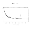
- FIG. 11 shows experimental results to determine whether a chromium oxide layer having an alpha-phase crystalline structure has an effect on an aluminum oxide layer having a gamma-phase crystalline structure
- FIG. 12 shows experimental results to determine the effect of a densification process for an amorphous aluminum oxide layer in the method of forming the alpha aluminum oxide layer described in FIGS. 1-3 .
- first”, “second”, etc. may be used herein to describe various elements, components, regions, layers and/or sections, these elements, components, regions, layers and/or sections should not be limited by these terms. These terms are only used to distinguish one element, component, region, layer or section from another element, component, region, layer or section. Thus, a first element, component, region, layer or section discussed below could be termed a second element, component, region, layer or section without departing from the teachings of example embodiments.
- spatially relative terms such as “beneath,” “below,” “lower,” “above,” “upper” and the like, may be used herein for ease of description to describe one element or feature's relationship to another element(s) or feature(s) as illustrated in the figures. It will be understood that the spatially relative terms are intended to encompass different orientations of the device in use or operation in addition to the orientation depicted in the figures. For example, if the device in the figures is turned over, elements described as “below” or “beneath” other elements or features would then be oriented “above” the other elements or features. Thus, the exemplary term “below” can encompass both an orientation of above and below. The device may be otherwise oriented (rotated 90 degrees or at other orientations) and the spatially relative descriptors used herein interpreted accordingly.
- Example embodiments are described herein with reference to cross-sectional illustrations that are schematic illustrations of idealized embodiments (and intermediate structures) of example embodiments. As such, variations from the shapes of the illustrations as a result, for example, of manufacturing techniques and/or tolerances, are to be expected. Thus, example embodiments should not be construed as limited to the particular shapes of regions illustrated herein but are to include deviations in shapes that result, for example, from manufacturing. For example, an implanted region illustrated as a rectangle will, typically, have rounded or curved features and/or a gradient of implant concentration at its edges rather than a binary change from implanted to non-implanted region.
- a buried region formed by implantation may result in some implantation in the region between the buried region and the surface through which the implantation takes place.
- the regions illustrated in the figures are schematic in nature and their shapes are not intended to illustrate the actual shape of a region of a device and are not intended to limit the scope of example embodiments.
- a method of forming an alpha-phase crystalline aluminum oxide ( ⁇ -Al 2 O 3 ) layer which has the largest energy band gap and the smallest defect density from among a plurality of aluminum oxides, may be used in a process for manufacturing a charge trap memory device, for example, in a process for forming a blocking oxide layer, thereby enhancing the charge retention capability of the charge trap memory device.
- the method of forming the alpha-phase crystalline aluminum oxide ( ⁇ -Al 2 O 3 ) layer for e ⁇ ample, the aluminum oxide layer having the alpha-phase crystalline structure (hereinafter, referred to as ‘an alpha aluminum oxide layer’) according to example embodiments will be now described.
- an amorphous aluminum oxide layer 12 a may be formed on an underlying layer 10 .
- the amorphous aluminum oxide layer 12 a may be an Al 2 O 3 layer.
- the amorphous aluminum oxide layer 12 a may be formed using various deposition methods, e.g., an atomic layer deposition (ALD) method, a sputtering vapor deposition method and/or a chemical vapor deposition (CVD) method.
- An amorphous chromium oxide layer 14 a may be formed on the amorphous aluminum oxide layer 12 a .
- the amorphous chromium oxide layer 14 a may be a Cr 2 O 3 layer.
- the amorphous chromium oxide layer 14 a may be formed using the same methods as the methods for forming the amorphous aluminum oxide layer 12 a.
- the amorphous chromium oxide layer 14 a may be thermally treated (hereinafter, referred to as ‘a first thermal treatment’) so as to be crystallized.
- the first thermal treatment may be performed at a temperature that does not affect crystallization of the amorphous aluminum oxide layer 12 a .
- the first thermal treatment may be performed at a temperature of about 600° C. to about 900° C., for example, below about 700° C., so as not to affect the amorphous aluminum oxide layer 12 a . Due to the first thermal treatment, the amorphous chromium oxide layer 14 a may change into a chromium oxide layer 14 having an alpha-phase crystalline structure, as illustrated in FIG. 2 .
- FIG. 8 shows graph results of an X-ray diffraction analysis experiment conducted so as to confirm whether the crystalline chromium oxide layer 14 formed by performing the first thermal treatment has an alpha-phase crystalline structure.
- a first graph G 1 represents the result regarding the amorphous chromium oxide layer 14 a
- a second graph G 2 represents the X-ray diffraction analysis result regarding the resultant product obtained by forming and thermally treating the amorphous chromium oxide layer 14 a at a temperature of about 600° C
- a third graph G 3 represents the X-ray diffraction analysis result regarding the resultant product obtained by forming and thermally treating the amorphous chromium oxide layer 14 a at a temperature of about 700° C.
- a thermal treatment (hereinafter, referred to as ‘a second thermal treatment) may be performed so as to crystallize the amorphous aluminum oxide layer 12 a into an alpha-phase crystalline structure.
- An alpha-phase nucleation in a nano size may be caused because the chromium oxide layer 14 having the alpha-phase crystalline structure exists.
- the second thermal treatment may be performed at a temperature of about 1000° C.
- an alpha aluminium oxide layer 12 may be formed.
- the chromium oxide layer 14 having the alpha-phase crystalline structure may be removed. If the thickness of the chromium oxide layer 14 is sufficiently small, removing the chromium oxide layer 14 may not be necessary.
- FIG. 9 shows the results of the experiment.
- a first graph G 11 represents the X-ray diffraction analysis result regarding an output obtained by thermal treating a test specimen at a temperature of about 1100° C., wherein the test specimen does not include the amorphous chromium oxide (Cr 2 O 3 ) layer 14 a but only includes the amorphous aluminum oxide (Al 2 O 3 ) layer 12 a .
- a peak P 1 of the first graph G 11 represents that a crystalline aluminum oxide (Al 2 O 3 ) layer, which may be thermal treated at a temperature of about 1100° C. without including the amorphous chromium oxide (Cr 2 O 3 ) layer 14 a and formed thereof, has a gamma-phase crystalline structure.
- a second graph G 22 represents the X-ray diffraction analysis result obtained by measuring the resultant product after forming the amorphous chromium oxide layer 14 a on the amorphous aluminum oxide layer 12 a and then thermally treating the resultant product at a temperature of about 700° C.
- a third graph G 33 represents the result obtained by measuring the resultant product obtained by forming the amorphous chromium oxide layer 14 a on the amorphous aluminum oxide layer 12 a and then thermally treating each of the amorphous chromium oxide layer 14 a and the amorphous aluminum oxide layer 12 a at a temperature of about 700° C. and about 1050° C.
- a fourth graph G 44 represents the result obtained by measuring the resultant product obtained by forming the amorphous chromium oxide layer 14 a on the amorphous aluminum oxide layer 12 a and then thermally treating the resultant product at a temperature of about 1050° C.
- the peak P 1 shown in the first graph G 11 is not shown in the second through fourth graphs G 22 , G 33 , and G 44 .
- formation of the aluminum oxide layer having the gamma-phase crystalline structure may be restrained.
- the alpha-phase nucleation may be caused by the alpha-phase chromium oxide layer 14 when the chromium oxide layer 14 having the alpha-phase crystalline structure exists on the amorphous aluminum oxide layer 12 a and thus, a crystalline structure of the crystalline aluminium oxide layer 12 crystallized by the thermal treatment may be in an alpha-phase.
- FIG. 10 illustrates Transmission Electron Microscope (TEM) pictures of a crystallized sample obtained by depositing an amorphous chromium oxide layer on an amorphous aluminum oxide layer and then performing a thermal treatment at a temperature of about 900° C.
- TEM Transmission Electron Microscope
- FIG. 11 illustrates the results of an experiment conducted so as to determine whether a chromium oxide layer having an alpha-phase crystalline structure has an effect on an aluminum oxide layer having a gamma-phase crystalline structure.
- the resultant product may be obtained by depositing an amorphous chromium oxide layer on a crystalline aluminum oxide layer which has been thermally treated at a temperature of about 1100° C., and then by thermally treating the resultant product at a temperature of about 900° C. for crystallization.
- a crystalline structure of the aluminum oxide layer which has already been crystallized into the gamma-phase due to the thermal treatment at a temperature of about 1100° C., remains in the gamma-phase without being transformed to an alpha-phase, even though the alpha-phase chromium oxide layer may be used.
- the method of forming the alpha aluminum oxide layer described in relation to FIGS. 1-3 is used in a method of manufacturing a semiconductor device, for example, in a method of manufacturing a charge trap memory device, the method of forming the alpha aluminum oxide layer may be used in a process of forming a blocking insulation layer.
- the chromium oxide layer 14 having the alpha-phase crystalline structure instead of using the chromium oxide layer 14 having the alpha-phase crystalline structure, other material layers which cause the alpha-phase nucleation may be used. Such examples are an alpha-FeO 3 layer, a Ga 2 O 3 layer, an Rh 2 O 3 layer, a Ti 2 O 3 layer, a V 2 O 3 layer, a gamma-Al 2 S 3 layer and/or a Co 2 As 3 layer.
- the chromium oxide layer 14 having the alpha-phase crystalline structure and the other material layers may decrease the crystallization temperature when the alpha aluminum oxide layer 12 is formed.
- the chromium oxide layer 14 having the alpha-phase crystalline structure and the other material layers may be a crystallization temperature decrease layer, or a crystalline auxiliary layer which decreases the crystallization temperature.
- the amorphous chromium oxide layer 14 a may be an amorphous temperature decrease layer or an amorphous auxiliary layer.
- a densification process may be performed on the amorphous aluminum oxide layer 12 a before or after the amorphous chromium oxide layer 14 a is formed.
- the densification process may be performed before the amorphous chromium oxide layer 14 a is formed.
- the densification process may be performed at a temperature that does not affect crystallization of the amorphous aluminum oxide layer 12 a .
- the densification process may be performed at a temperature below about 800° C.
- FIG. 12 shows the result of the experiment to determine the effect of the densification process.
- a first graph GG 1 represents the X-ray diffraction analysis result regarding the resultant product obtained by thermally treating a test specimen at a temperature of about 1100° C., wherein the test specimen does not include the amorphous chromium oxide (Cr 2 O 3 ) layer 14 a but only includes the amorphous aluminum oxide (Al 2 O 3 ) layer 12 a .
- a peak P 11 of the first graph GG 1 represents that a crystalline aluminum oxide (Al 2 O 3 ) layer, which may be thermally treated at a temperature of about 1100° C. without including the amorphous chromium oxide (Cr 2 O 3 ) layer 14 a and formed thereof, has a gamma-phase crystalline structure.
- a second graph GG 2 represents the X-ray diffraction analysis result obtained by measuring the resultant product from forming the amorphous chromium oxide layer 14 a on the amorphous aluminum oxide layer 12 a and then thermally treating the output at a temperature of about 700° C.
- a third graph GG 3 represents the result obtained by measuring the resultant product from forming the amorphous chromium oxide layer 14 a on the amorphous aluminum oxide layer 12 a and then thermally treating the amorphous chromium oxide layer 14 a and the amorphous aluminum oxide layer 12 a at a temperature of about 700° C. and about 1050° C.
- a fourth graph GG 4 represents the result obtained by measuring the resultant product from forming the amorphous chromium oxide layer 14 a on the amorphous aluminum oxide layer 12 a and then thermally treating the amorphous chromium oxide layer 14 a and the amorphous aluminum oxide layer 12 a at a temperature of about 1050° C.
- the gamma-phase crystalline structure and the alpha-phase crystalline structure may be mixed in the crystalline aluminium oxide layer 12 in the second through fourth graphs GG 2 , GG 3 , and GG 4 of FIG. 12 .
- a tunnelling film 16 may be formed on a substrate 40 .
- the substrate 40 may be a silicon substrate.
- the tunnelling film 16 may be formed by a thermal oxidation method.
- a charge storage layer 18 may be formed on the tunnelling film 16 .
- the charge storage layer 18 may be formed by a low-pressure chemical vapour deposition (LPCVD) method or other laminating methods.
- the charge storage layer 18 may include one of a silicon nitride layer, e.g., a Si 3 N 4 layer, a metal nano dot, and a silicon nano dot.
- the charge storage layer 18 may be formed to have a multi-layer structure or a mixed structure including at least two of the silicon nitride layer, the metal nano dot, and the silicon nano dot.
- the charge storage layer 18 may be one of a doped polysilicon film, a silicon nitride film, an Hf0 2 film, a La 2 0 3 film, and a Zr0 2 film, or may be a mixture including at least two of the doped polysilicon film, the silicon nitride film, the Hf0 2 film, the La 2 0 3 film, and the Zr0 2 film.
- a blocking insulation layer 20 may be formed thereon.
- the blocking insulation layer 20 may be an alpha aluminium oxide layer.
- the blocking insulation layer 20 may be formed by using the method described in relation to FIGS. 1-3 .
- a gate electrode 22 may be formed on the blocking insulation layer 20 .
- an alpha-phase crystalline chromium oxide layer 14 formed on the blocking insulation layer 20 may be removed before the gate electrode 22 is formed.
- a work function of the gate electrode 22 may be over about 4.0 eV.
- the gate electrode 22 may be a TaN electrode (tantalum nitride).
- the gate electrode 22 and the layers 20 , 18 , and 16 beneath the gate electrode 22 may be sequentially etched by the circumference of the mask M 1 .
- FIG. 6 illustrates a result of the etching.
- a gate laminate GS may be formed by the etching, wherein the gate laminate GS includes the tunnelling film 16 , the charge storage layer 18 , the blocking insulation layer 20 , and the gate electrode 22 .
- Conductive impurities may be injected in the substrate 40 which may be exposed by the etching, so that first and second shallow impurity regions 30 a and 32 a may be formed on the substrate 40 .
- the mask M 1 may be removed.
- the mask M 1 may be removed before the first and second shallow impurity regions 30 a and 32 a are formed.
- a gate spacer 24 may be formed on a side surface of the gate laminate GS.
- the gate spacer 24 may be formed by forming a raw material film on the substrate 40 , where the raw material film covers the gate laminate GS, and by performing an anisotropic etching on the raw material film until the substrate 40 may be exposed.
- conductive impurities may be injected in the substrate 40 so that each of first and second deep impurity regions 30 b and 32 b may be formed on the first and second shallow impurity regions 30 a and 32 a .
- first and second impurity regions 30 and 32 which have a lightly doped drain (LDD) structure, may be formed on the substrate 40 .
- One of the first and second impurity regions 30 and 32 may be a source region, and the other may be a drain region.
- LDD lightly doped drain
- the gate laminate GS may be covered with an interlayer insulating layer in a following process
- formation of the gate spacer 24 is optional. Where the formation of the gate spacer 24 may be omitted, the first and second impurity regions 30 and 32 may be the same as the first and second shallow impurity regions 30 a and 32 a.
- an aluminum oxide layer having an alpha-phase crystalline structure may be formed by using an auxiliary layer (for example, an alpha-phase chromium oxide layer).
- an auxiliary layer for example, an alpha-phase chromium oxide layer.
- the temperature at which the aluminum oxide layer having the alpha-phase crystalline structure is formed may be decreased to about 1000° C. or lower.
- example embodiments may prevent or reduce a side effect occurring when forming the aluminum oxide layer having an alpha-phase crystalline structure.
- Example embodiments may also prevent or reduce bending of the substrate under thermal stress.
- example embodiments may enhance the charge retention capability of a charge trap memory device by forming an aluminum oxide layer having an alpha-phase crystalline structure on the charge trap memory device.
- the alpha-phase crystalline chromium oxide layer may be directly deposited on the amorphous aluminum oxide layer, instead of crystallizing the amorphous chromium oxide layer and then forming the alpha-phase crystalline chromium oxide layer on the amorphous aluminum oxide layer.
- a metal layer may be formed if the alpha-phase nucleation occurs instead of the formation of the alpha-phase crystalline chromium oxide layer.
Abstract
Provided is a method of forming an aluminum oxide layer and a method of manufacturing a charge trap memory device using the same. The method of forming an aluminum oxide layer may include forming an amorphous aluminum oxide layer on an underlying layer, forming a crystalline auxiliary layer on the amorphous aluminum oxide layer, and crystallizing the amorphous aluminum oxide layer. Forming the crystalline auxiliary layer may include forming an amorphous auxiliary layer on the amorphous aluminum oxide layer; and crystallizing the amorphous auxiliary layer.
Description
This application claims priority under 35 U.S.C. §119 to Korean Patent Application No. 10-2007-0087290, filed on Aug. 29, 2007, in the Korean Intellectual Property Office (KIPO), the entire contents of which are incorporated herein by reference for all purposes as if fully set forth herein.
1. Field
Example embodiments relate to a method of manufacturing a semiconductor device, and more particularly, to a method of forming an aluminum oxide layer and a method of manufacturing a charge trap memory device using the same.
2. Description of the Related Art
Because the amount of data to be securely stored for a relatively long time may be increased and a data storage device, e.g., a memory stick, for moving a task result to another place may be provided, there is a need for a non-volatile memory device wherein data may be electrically stored and erased and which may conserve stored data even when power is not supplied.
Conventionally, increased capacity non-volatile memory devices, e.g., NAND flash memory devices, may be used. The NAND flash memory device may have a structure in which a floating gate for storing charges (e.g., data) and a control gate for controlling the storing of charges in the floating gate may be sequentially laminated. However, the floating gate may include a conductive material, e.g., doped polysilicon, which may cause increased parasitic capacitance between adjacent memory cells when higher integration is desired.
Accordingly, in order to solve the aforementioned problem of the conventional NAND flash memory device, there has been research on non-volatile memory devices referred to as Metal-Oxide-Insulator-Oxide-Semiconductor (MOIOS) memory devices, e.g., Silicon-Oxide-Nitride-Oxide-Semiconductor (SONOS) memory devices or Metal-Oxide-Nitride-Oxide-Semiconductor (MONOS) memory devices. The SONOS memory device may use silicon as a material for the control gate, but the MONOS memory device may use a metal as the material for the control gate.
The MOIOS memory device may include a charge trap layer, e.g., a silicon nitride (Si3N4) film, instead of a floating gate, which includes polysilicon, in order to store charges. For example, a structure of a memory cell in the MOIOS memory device may include an oxide film, a nitride film, and an oxide film, which may be sequentially laminated between a substrate and the control gate. The MOIOS memory device may use a characteristic, whereby a threshold voltage may be shifted as charges may be trapped in the nitride film.
A dielectric constant of the silicon nitride film and a silicon-oxide film in the conventional MOIOS memory device, e.g., the SONOS memory device, may be relatively low. Thus, the conventional MOIOS memory device may have an increased operation voltage, decreased speed for recording (programming) and erasing data, and relatively short retention time (a time during which stored data may be conserved). One method to increase the retention time may be to use an aluminum oxide (Al2O3) layer, which has an alpha-phase crystalline structure, as a blocking layer.
The aluminum oxide (Al2O3) layer having the alpha-phase crystalline structure may be formed by thermal treating an amorphous aluminum oxide (Al2O3) layer at a temperature higher than about 1200° C. However, a silicon substrate may bend due to thermal stress from the thermal treatment process. Hence, the aluminum oxide (Al2O3) layer having the alpha-phase crystalline structure may be difficult to use as the blocking layer.
Example embodiments provide a method of forming an aluminum oxide layer without damaging a substrate. Example embodiments also provide a method of manufacturing a charge trap memory device by using the method of forming an aluminum oxide layer, thereby enhancing a charge retention capability of the charge trap memory device.
According to example embodiments, a method of forming an alpha aluminum oxide layer may include forming an amorphous aluminum oxide layer on an underlying layer, forming a crystalline auxiliary layer on the amorphous aluminum oxide layer, and crystallizing the amorphous aluminum oxide layer.
The method may further include removing the crystalline auxiliary layer. The underlying layer may be formed of a charge storage material. The charge storage material may be a silicon nitride. A densification process for the amorphous aluminum oxide layer may be performed before the crystalline auxiliary layer may be formed. Forming the crystalline auxiliary layer may include forming an amorphous auxiliary layer on the amorphous aluminum oxide layer, and crystallizing the amorphous auxiliary layer. The densification process for the amorphous aluminum oxide layer may be performed before the amorphous auxiliary layer may be formed. The crystallization of the amorphous auxiliary layer and the crystallization of the amorphous aluminum oxide layer may be simultaneously performed at a temperature below about 1000° C.
The crystalline auxiliary layer may be one of a Cr2O3 layer having an alpha-phase crystalline structure, an alpha-FeO3 layer, a Ga2O3 layer, an Rh2O3 layer, a Ti2O3 layer, a V2O3 layer, a gamma-Al2S3 layer, and a Co2As3 layer. The crystallization of the amorphous auxiliary layer may be performed at a temperature lower than the temperature for the crystallization of the amorphous aluminum oxide layer. The crystallization of the amorphous auxiliary layer may be performed at a temperature below about 800° C. In removing the crystalline auxiliary layer, the crystalline auxiliary layer may be partially removed.
According to example embodiments, a method of manufacturing a charge trap memory device may include forming a tunneling film, a charge storage layer, a blocking insulation layer, and a gate electrode on a substrate, wherein forming the blocking insulation layer includes forming the alpha aluminum oxide layer according to example embodiments, in which the charge storage layer may be the underlying layer.
Forming the charge storage layer may include forming one of a silicon nitride film, a metal nano dot, and a silicon nano dot. The charge storage layer may be formed to have a multi-layer structure or a mixed structure which includes at least two of the silicon nitride film, the metal nano dot, and the silicon nano dot. Also, the charge storage layer may be one of a doped polysilicon film, a silicon nitride film, an Hf02 film, a La203 film, and a Zr02 film or the charge storage layer may be one of mixtures including at least two of the doped polysilicon film, the silicon nitride film, the Hf02 film, the La203 film, and the Zr02 film. A work function of the gate electrode may be over about 4.0 eV. Forming the gate electrode may include forming a TaN (tantalum nitride) electrode.
The patent or application file contains at least one drawing executed in color. Copies of this patent or patent application publication with color drawing will be provided by the Office upon request and payment of the necessary fee.
Example embodiments will be more clearly understood from the following detailed description taken in conjunction with the accompanying drawings. FIGS. 1-12 represent non-limiting, example embodiments as described herein.
It should be noted that these Figures are intended to illustrate the general characteristics of methods, structure and/or materials utilized in certain example embodiments and to supplement the written description provided below. These drawings are not, however, to scale and may not precisely reflect the precise structural or performance characteristics of any given embodiment, and should not be interpreted as defining or limiting the range of values or properties encompassed by example embodiments. In particular, the relative thicknesses and positioning of molecules, layers, regions and/or structural elements may be reduced or exaggerated for clarity. The use of similar or identical reference numbers in the various drawings is intended to indicate the presence of a similar or identical element or feature.
Hereinafter, a method of forming an aluminum oxide layer having an alpha-phase crystalline structure and a method of manufacturing a charge trap memory device using the same according to example embodiments will now be described more fully with reference to the accompanying drawings, in which exemplary embodiments may be shown. In the drawings, the thicknesses of layers and regions are exaggerated for clarity.
It will be understood that when an element is referred to as being “connected” or “coupled” to another element, it can be directly connected or coupled to the other element or intervening elements may be present. In contrast, when an element is referred to as being “directly connected” or “directly coupled” to another element, there are no intervening elements present. Like numbers indicate like elements throughout. As used herein the term “and/or” includes any and all combinations of one or more of the associated listed items.
It will be understood that, although the terms “first”, “second”, etc. may be used herein to describe various elements, components, regions, layers and/or sections, these elements, components, regions, layers and/or sections should not be limited by these terms. These terms are only used to distinguish one element, component, region, layer or section from another element, component, region, layer or section. Thus, a first element, component, region, layer or section discussed below could be termed a second element, component, region, layer or section without departing from the teachings of example embodiments.
Spatially relative terms, such as “beneath,” “below,” “lower,” “above,” “upper” and the like, may be used herein for ease of description to describe one element or feature's relationship to another element(s) or feature(s) as illustrated in the figures. It will be understood that the spatially relative terms are intended to encompass different orientations of the device in use or operation in addition to the orientation depicted in the figures. For example, if the device in the figures is turned over, elements described as “below” or “beneath” other elements or features would then be oriented “above” the other elements or features. Thus, the exemplary term “below” can encompass both an orientation of above and below. The device may be otherwise oriented (rotated 90 degrees or at other orientations) and the spatially relative descriptors used herein interpreted accordingly.
The terminology used herein is for the purpose of describing particular embodiments only and is not intended to be limiting of example embodiments. As used herein, the singular forms “a,” “an” and “the” are intended to include the plural forms as well, unless the context clearly indicates otherwise. It will be further understood that the terms “comprises” and/or “comprising,” when used in this specification, specify the presence of stated features, integers, steps, operations, elements, and/or components, but do not preclude the presence or addition of one or more other features, integers, steps, operations, elements, components, and/or groups thereof.
Example embodiments are described herein with reference to cross-sectional illustrations that are schematic illustrations of idealized embodiments (and intermediate structures) of example embodiments. As such, variations from the shapes of the illustrations as a result, for example, of manufacturing techniques and/or tolerances, are to be expected. Thus, example embodiments should not be construed as limited to the particular shapes of regions illustrated herein but are to include deviations in shapes that result, for example, from manufacturing. For example, an implanted region illustrated as a rectangle will, typically, have rounded or curved features and/or a gradient of implant concentration at its edges rather than a binary change from implanted to non-implanted region. Likewise, a buried region formed by implantation may result in some implantation in the region between the buried region and the surface through which the implantation takes place. Thus, the regions illustrated in the figures are schematic in nature and their shapes are not intended to illustrate the actual shape of a region of a device and are not intended to limit the scope of example embodiments.
Unless otherwise defined, all terms (including technical and scientific terms) used herein have the same meaning as commonly understood by one of ordinary skill in the art to which example embodiments belong. It will be further understood that terms, such as those defined in commonly-used dictionaries, should be interpreted as having a meaning that is consistent with their meaning in the context of the relevant art and will not be interpreted in an idealized or overly formal sense unless expressly so defined herein.
In example embodiments, a method of forming an alpha-phase crystalline aluminum oxide (α-Al2O3) layer, which has the largest energy band gap and the smallest defect density from among a plurality of aluminum oxides, may be used in a process for manufacturing a charge trap memory device, for example, in a process for forming a blocking oxide layer, thereby enhancing the charge retention capability of the charge trap memory device. The method of forming the alpha-phase crystalline aluminum oxide (α-Al2O3) layer, for e×ample, the aluminum oxide layer having the alpha-phase crystalline structure (hereinafter, referred to as ‘an alpha aluminum oxide layer’) according to example embodiments will be now described.
Referring to FIG. 1 , an amorphous aluminum oxide layer 12 a may be formed on an underlying layer 10. The amorphous aluminum oxide layer 12 a may be an Al2O3 layer. The amorphous aluminum oxide layer 12 a may be formed using various deposition methods, e.g., an atomic layer deposition (ALD) method, a sputtering vapor deposition method and/or a chemical vapor deposition (CVD) method. An amorphous chromium oxide layer 14 a may be formed on the amorphous aluminum oxide layer 12 a. The amorphous chromium oxide layer 14 a may be a Cr2O3 layer. The amorphous chromium oxide layer 14 a may be formed using the same methods as the methods for forming the amorphous aluminum oxide layer 12 a.
The amorphous chromium oxide layer 14 a may be thermally treated (hereinafter, referred to as ‘a first thermal treatment’) so as to be crystallized. The first thermal treatment may be performed at a temperature that does not affect crystallization of the amorphous aluminum oxide layer 12 a. For example, the first thermal treatment may be performed at a temperature of about 600° C. to about 900° C., for example, below about 700° C., so as not to affect the amorphous aluminum oxide layer 12 a. Due to the first thermal treatment, the amorphous chromium oxide layer 14 a may change into a chromium oxide layer 14 having an alpha-phase crystalline structure, as illustrated in FIG. 2 .
In FIG. 8 , a first graph G1 represents the result regarding the amorphous chromium oxide layer 14 a, and a second graph G2 represents the X-ray diffraction analysis result regarding the resultant product obtained by forming and thermally treating the amorphous chromium oxide layer 14 a at a temperature of about 600° C. Also, a third graph G3 represents the X-ray diffraction analysis result regarding the resultant product obtained by forming and thermally treating the amorphous chromium oxide layer 14 a at a temperature of about 700° C.
Comparing the first graph G1 to the second and third graphs G2 and G3, various peaks, which are not shown in the first graph G1, are shown in the second and third graphs G2 and G3. Because such peaks may be found in a chromium oxide layer having the alpha-phase crystalline structure, a crystalline structure of the crystalline chromium oxide layer 14 may be in an alpha-phase, wherein the crystalline chromium oxide layer 14 may be obtained by thermally treating the amorphous chromium oxide layer 14 a at a temperature below about 700° C.
After the chromium oxide layer 14 having the alpha-phase crystalline structure may be obtained by thermally treating the amorphous chromium oxide layer 14 a, a thermal treatment (hereinafter, referred to as ‘a second thermal treatment) may be performed so as to crystallize the amorphous aluminum oxide layer 12 a into an alpha-phase crystalline structure. An alpha-phase nucleation in a nano size may be caused because the chromium oxide layer 14 having the alpha-phase crystalline structure exists. Thus, the second thermal treatment may be performed at a temperature of about 1000° C. As a result of the second thermal treatment, as illustrated in FIG. 3 , an alpha aluminium oxide layer 12 may be formed. After that, the chromium oxide layer 14 having the alpha-phase crystalline structure may be removed. If the thickness of the chromium oxide layer 14 is sufficiently small, removing the chromium oxide layer 14 may not be necessary.
An experiment was conducted for confirming whether the crystalline aluminium oxide layer 12 formed by performing the second thermal treatment has an alpha-phase crystalline structure. FIG. 9 shows the results of the experiment.
In FIG. 9 , a first graph G11 represents the X-ray diffraction analysis result regarding an output obtained by thermal treating a test specimen at a temperature of about 1100° C., wherein the test specimen does not include the amorphous chromium oxide (Cr2O3) layer 14 a but only includes the amorphous aluminum oxide (Al2O3) layer 12 a. A peak P1 of the first graph G11 represents that a crystalline aluminum oxide (Al2O3) layer, which may be thermal treated at a temperature of about 1100° C. without including the amorphous chromium oxide (Cr2O3) layer 14 a and formed thereof, has a gamma-phase crystalline structure.
In FIG. 9 , a second graph G22 represents the X-ray diffraction analysis result obtained by measuring the resultant product after forming the amorphous chromium oxide layer 14 a on the amorphous aluminum oxide layer 12 a and then thermally treating the resultant product at a temperature of about 700° C. A third graph G33 represents the result obtained by measuring the resultant product obtained by forming the amorphous chromium oxide layer 14 a on the amorphous aluminum oxide layer 12 a and then thermally treating each of the amorphous chromium oxide layer 14 a and the amorphous aluminum oxide layer 12 a at a temperature of about 700° C. and about 1050° C. so as to crystallize the amorphous chromium oxide layer 14 a and the amorphous aluminum oxide layer 12 a. Also, a fourth graph G44 represents the result obtained by measuring the resultant product obtained by forming the amorphous chromium oxide layer 14 a on the amorphous aluminum oxide layer 12 a and then thermally treating the resultant product at a temperature of about 1050° C.
Comparing the first graph G11 to the second through fourth graphs G22, G33, and G44, the peak P1 shown in the first graph G11 is not shown in the second through fourth graphs G22, G33, and G44. Thus, with test samples corresponding to the second through fourth graphs G22, G33, and G44, formation of the aluminum oxide layer having the gamma-phase crystalline structure may be restrained.
Such results suggest that the alpha-phase nucleation may be caused by the alpha-phase chromium oxide layer 14 when the chromium oxide layer 14 having the alpha-phase crystalline structure exists on the amorphous aluminum oxide layer 12 a and thus, a crystalline structure of the crystalline aluminium oxide layer 12 crystallized by the thermal treatment may be in an alpha-phase.
Referring to FIG. 10 , a chromium oxide layer and an aluminum oxide layer, which have an alpha-phase crystalline structure, may be formed. FIG. 11 illustrates the results of an experiment conducted so as to determine whether a chromium oxide layer having an alpha-phase crystalline structure has an effect on an aluminum oxide layer having a gamma-phase crystalline structure. In the experiment, the resultant product may be obtained by depositing an amorphous chromium oxide layer on a crystalline aluminum oxide layer which has been thermally treated at a temperature of about 1100° C., and then by thermally treating the resultant product at a temperature of about 900° C. for crystallization.
Referring to FIG. 11 , considering the position of a peak P2, a crystalline structure of the aluminum oxide layer, which has already been crystallized into the gamma-phase due to the thermal treatment at a temperature of about 1100° C., remains in the gamma-phase without being transformed to an alpha-phase, even though the alpha-phase chromium oxide layer may be used.
Where the method of forming the alpha aluminum oxide layer described in relation to FIGS. 1-3 is used in a method of manufacturing a semiconductor device, for example, in a method of manufacturing a charge trap memory device, the method of forming the alpha aluminum oxide layer may be used in a process of forming a blocking insulation layer.
Also, instead of using the chromium oxide layer 14 having the alpha-phase crystalline structure, other material layers which cause the alpha-phase nucleation may be used. Such examples are an alpha-FeO3 layer, a Ga2O3 layer, an Rh2O3 layer, a Ti2O3 layer, a V2O3 layer, a gamma-Al2S3 layer and/or a Co2As3 layer. The chromium oxide layer 14 having the alpha-phase crystalline structure and the other material layers may decrease the crystallization temperature when the alpha aluminum oxide layer 12 is formed. Thus, the chromium oxide layer 14 having the alpha-phase crystalline structure and the other material layers may be a crystallization temperature decrease layer, or a crystalline auxiliary layer which decreases the crystallization temperature. Accordingly, the amorphous chromium oxide layer 14 a may be an amorphous temperature decrease layer or an amorphous auxiliary layer.
Also, a densification process may be performed on the amorphous aluminum oxide layer 12 a before or after the amorphous chromium oxide layer 14 a is formed. For example, the densification process may be performed before the amorphous chromium oxide layer 14 a is formed. The densification process may be performed at a temperature that does not affect crystallization of the amorphous aluminum oxide layer 12 a. For example, the densification process may be performed at a temperature below about 800° C.
An experiment was conducted to determine how the densification process affects the formation of the alpha aluminum oxide layer 12. Except for the fact that the densification process was performed on the amorphous aluminum oxide layer 12 a before the amorphous chromium oxide layer 14 a was formed, the experiment was conducted identically to the experiment for obtaining the result shown in FIG. 9 . A thermal treatment for densification of the amorphous aluminum oxide layer 12 a was performed at a temperature of about 800° C.
In FIG. 12 , a second graph GG2 represents the X-ray diffraction analysis result obtained by measuring the resultant product from forming the amorphous chromium oxide layer 14 a on the amorphous aluminum oxide layer 12 a and then thermally treating the output at a temperature of about 700° C. A third graph GG3 represents the result obtained by measuring the resultant product from forming the amorphous chromium oxide layer 14 a on the amorphous aluminum oxide layer 12 a and then thermally treating the amorphous chromium oxide layer 14 a and the amorphous aluminum oxide layer 12 a at a temperature of about 700° C. and about 1050° C. so as to crystallize the amorphous chromium oxide layer 14 a and the amorphous aluminum oxide layer 12 a. Also, a fourth graph GG4 represents the result obtained by measuring the resultant product from forming the amorphous chromium oxide layer 14 a on the amorphous aluminum oxide layer 12 a and then thermally treating the amorphous chromium oxide layer 14 a and the amorphous aluminum oxide layer 12 a at a temperature of about 1050° C.
Comparing the first graph GG1 to the second through fourth graphs GG2, GG3, and GG4, and comparing the second through fourth graphs G22, G33, and G44 in FIG. 9 to the second through fourth graphs GG2, GG3, and GG4 in FIG. 12 , the gamma-phase crystalline structure and the alpha-phase crystalline structure may be mixed in the crystalline aluminium oxide layer 12 in the second through fourth graphs GG2, GG3, and GG4 of FIG. 12 .
A method of manufacturing a charge trap memory device according to example embodiments will be described with reference to FIGS. 4-7 . Referring to FIG. 4 , a tunnelling film 16 may be formed on a substrate 40. The substrate 40 may be a silicon substrate. The tunnelling film 16 may be formed by a thermal oxidation method. A charge storage layer 18 may be formed on the tunnelling film 16. The charge storage layer 18 may be formed by a low-pressure chemical vapour deposition (LPCVD) method or other laminating methods. The charge storage layer 18 may include one of a silicon nitride layer, e.g., a Si3N4 layer, a metal nano dot, and a silicon nano dot. Also, the charge storage layer 18 may be formed to have a multi-layer structure or a mixed structure including at least two of the silicon nitride layer, the metal nano dot, and the silicon nano dot. The charge storage layer 18 may be one of a doped polysilicon film, a silicon nitride film, an Hf02 film, a La 203 film, and a Zr02 film, or may be a mixture including at least two of the doped polysilicon film, the silicon nitride film, the Hf02 film, the La 203 film, and the Zr02 film.
After the charge storage layer 18 is formed, a blocking insulation layer 20 may be formed thereon. The blocking insulation layer 20 may be an alpha aluminium oxide layer. The blocking insulation layer 20 may be formed by using the method described in relation to FIGS. 1-3 . A gate electrode 22 may be formed on the blocking insulation layer 20. For example, an alpha-phase crystalline chromium oxide layer 14 formed on the blocking insulation layer 20 may be removed before the gate electrode 22 is formed. However, if the thickness of the alpha-phase crystalline chromium oxide layer 14 is sufficiently small, the alpha-phase crystalline chromium oxide layer 14 may not be removed. A work function of the gate electrode 22 may be over about 4.0 eV. For example, the gate electrode 22 may be a TaN electrode (tantalum nitride).
Referring to FIG. 5 , after a mask M1 is formed on the gate electrode 22, the gate electrode 22 and the layers 20, 18, and 16 beneath the gate electrode 22 may be sequentially etched by the circumference of the mask M1.
Referring to FIG. 7 , a gate spacer 24 may be formed on a side surface of the gate laminate GS. The gate spacer 24 may be formed by forming a raw material film on the substrate 40, where the raw material film covers the gate laminate GS, and by performing an anisotropic etching on the raw material film until the substrate 40 may be exposed. After the gate spacer 24 is formed, conductive impurities may be injected in the substrate 40 so that each of first and second deep impurity regions 30 b and 32 b may be formed on the first and second shallow impurity regions 30 a and 32 a. As a result, first and second impurity regions 30 and 32, which have a lightly doped drain (LDD) structure, may be formed on the substrate 40. One of the first and second impurity regions 30 and 32 may be a source region, and the other may be a drain region.
Considering that the gate laminate GS may be covered with an interlayer insulating layer in a following process, formation of the gate spacer 24 is optional. Where the formation of the gate spacer 24 may be omitted, the first and second impurity regions 30 and 32 may be the same as the first and second shallow impurity regions 30 a and 32 a.
In the method of forming a memory device according to example embodiments, an aluminum oxide layer having an alpha-phase crystalline structure may be formed by using an auxiliary layer (for example, an alpha-phase chromium oxide layer). By using the auxiliary layer, the temperature at which the aluminum oxide layer having the alpha-phase crystalline structure is formed may be decreased to about 1000° C. or lower. Thus, example embodiments may prevent or reduce a side effect occurring when forming the aluminum oxide layer having an alpha-phase crystalline structure. Example embodiments may also prevent or reduce bending of the substrate under thermal stress. Also, example embodiments may enhance the charge retention capability of a charge trap memory device by forming an aluminum oxide layer having an alpha-phase crystalline structure on the charge trap memory device.
While example embodiments have been particularly shown and described with reference to example embodiments thereof, it will be understood by those of ordinary skill in the art that various changes in form and details may be made therein without departing from the spirit and scope of the appended claims. For example, it will be understood by those of ordinary skill in the art that the alpha-phase crystalline chromium oxide layer may be directly deposited on the amorphous aluminum oxide layer, instead of crystallizing the amorphous chromium oxide layer and then forming the alpha-phase crystalline chromium oxide layer on the amorphous aluminum oxide layer. Also, if the alpha-phase nucleation occurs instead of the formation of the alpha-phase crystalline chromium oxide layer, a metal layer may be formed. Accordingly, these and other changes and modifications are within the true spirit and scope of the appended claims. In the specification, example embodiments have been disclosed. Although specific terms are employed, they are used in a generic and descriptive sense only and not for purposes of limitation, the scope being set forth in the following claims.
Claims (19)
1. A method of forming an alpha aluminum oxide layer comprising:
forming an amorphous aluminum oxide layer on an underlying layer;
forming a crystalline auxiliary layer on the amorphous aluminum oxide layer; and
crystallizing the amorphous aluminum oxide layer such that the amorphous aluminum oxide layer becomes an aluminum oxide layer including an alpha-phase crystalline structure by using the crystalline auxiliary layer.
2. The method of claim 1 , further comprising:
removing the crystalline auxiliary layer.
3. The method of claim 1 , wherein the underlying layer is made of a charge storage material.
4. The method of claim 3 , wherein the charge storage material is silicon nitride.
5. The method of claim 1 , wherein forming the crystalline auxiliary layer comprises:
forming an amorphous auxiliary layer on the amorphous aluminum oxide layer; and
crystallizing the amorphous auxiliary layer.
6. The method of claim 1 , wherein before forming the crystalline auxiliary layer, a densification process is performed on the amorphous aluminum oxide layer.
7. The method of claim 5 , wherein the densification process for the amorphous aluminum oxide layer is performed before the amorphous auxiliary layer is formed.
8. The method of claim 5 , wherein the crystallization of the amorphous auxiliary layer and the crystallization of the amorphous aluminum oxide layer are simultaneously performed at a temperature below about 1000° C.
9. The method of claim 1 , wherein the crystalline auxiliary layer is one of a Cr2O3 layer having an alpha-phase crystalline structure, an alpha-FeO3 layer, a Ga2O3 layer, an Rh2O3 layer, a Ti2O3 layer, a V2O3 layer, a gamma-Al2S3 layer, and a Co2As3 layer.
10. The method of claim 5 , wherein the crystallization of the amorphous auxiliary layer is performed at a temperature lower than a temperature for the crystallization of the amorphous aluminum oxide layer.
11. The method of claim 10 , wherein the crystallization of the amorphous auxiliary layer is performed at a temperature below about 800° C.
12. The method of claim 2 , wherein in removing the crystalline auxiliary layer, the crystalline auxiliary layer is partially removed.
13. The method of claim 5 , wherein the crystalline auxiliary layer is one of a Cr2O3 layer having the alpha-phase crystalline structure, an alpha-FeO3 layer, a Ga2O3 layer, an Rh2O3 layer, a Ti2O3 layer, a V2O3 layer, a gamma-Al2S3 layer, and a Co2As3 layer.
14. A method of manufacturing a charge trap memory device comprising:
forming a tunneling film, a charge storage layer, a blocking insulation layer, and a gate electrode on a substrate,
wherein forming the blocking insulation layer includes:
forming the alpha aluminum oxide layer according to claim 1 , in which the charge storage layer is the underlying layer.
15. The method of claim 14 , wherein forming the charge storage layer includes forming one of a silicon nitride film, a metal nano dot, and a silicon nano dot.
16. The method of claim 14 , wherein forming the charge storage layer includes forming a multi-layer structure or a mixed structure with at least two of a silicon nitride film, a metal nano dot, and a silicon nano dot.
17. The method of claim 14 , wherein forming the charge storage layer includes forming a doped polysilicon film, a silicon nitride film, an Hf02 film, a La203 film, and a Zr02 film or the charge storage layer is one of a mixture including at least two of the doped polysilicon film, the silicon nitride film, the Hf02 film, the La203 film, and the Zr02 film.
18. The method of claim 14 , wherein a work function of the gate electrode is over about 4.0 eV.
19. The method of claim 18 , wherein forming the gate electrode includes forming a TaN (tantalum nitride) electrode.
Applications Claiming Priority (2)
| Application Number | Priority Date | Filing Date | Title |
|---|---|---|---|
| KR1020070087290A KR101281682B1 (en) | 2007-08-29 | 2007-08-29 | Methods of forming aluminum oxide layer and manufacturing charge trap memory device using the same |
| KR10-2007-0087290 | 2007-08-29 |
Publications (2)
| Publication Number | Publication Date |
|---|---|
| US20090061613A1 US20090061613A1 (en) | 2009-03-05 |
| US8043952B2 true US8043952B2 (en) | 2011-10-25 |
Family
ID=40408141
Family Applications (1)
| Application Number | Title | Priority Date | Filing Date |
|---|---|---|---|
| US12/153,655 Active 2029-12-03 US8043952B2 (en) | 2007-08-29 | 2008-05-22 | Method of forming aluminum oxide layer and method of manufacturing charge trap memory device using the same |
Country Status (4)
| Country | Link |
|---|---|
| US (1) | US8043952B2 (en) |
| JP (1) | JP2009060102A (en) |
| KR (1) | KR101281682B1 (en) |
| CN (1) | CN101378013A (en) |
Families Citing this family (20)
| Publication number | Priority date | Publication date | Assignee | Title |
|---|---|---|---|---|
| JP5245287B2 (en) | 2007-05-18 | 2013-07-24 | ソニー株式会社 | Semiconductor device manufacturing method, thin film transistor substrate manufacturing method, and display device manufacturing method |
| US9932663B2 (en) | 2011-12-23 | 2018-04-03 | Hong Kong Baptist University | Sapphire thin film coated substrate |
| US10072329B2 (en) | 2011-12-23 | 2018-09-11 | Hong Kong Baptist University | Sapphire thin film coated flexible substrate |
| US11535926B2 (en) | 2011-12-23 | 2022-12-27 | Hkbu R&D Licensing Limited | Sapphire thin film coated substrate |
| US11713503B2 (en) | 2011-12-23 | 2023-08-01 | Hong Kong Baptist University | Sapphire coated substrate with a flexible, anti-scratch and multi-layer coating |
| TWI642552B (en) * | 2014-09-12 | 2018-12-01 | 香港浸會大學 | Sapphire thin film coated flexible substrate |
| US10446681B2 (en) | 2017-07-10 | 2019-10-15 | Micron Technology, Inc. | NAND memory arrays, and devices comprising semiconductor channel material and nitrogen |
| US10276411B2 (en) | 2017-08-18 | 2019-04-30 | Applied Materials, Inc. | High pressure and high temperature anneal chamber |
| US10559466B2 (en) | 2017-12-27 | 2020-02-11 | Micron Technology, Inc. | Methods of forming a channel region of a transistor and methods used in forming a memory array |
| US10297611B1 (en) * | 2017-12-27 | 2019-05-21 | Micron Technology, Inc. | Transistors and arrays of elevationally-extending strings of memory cells |
| CN111936664A (en) * | 2018-03-19 | 2020-11-13 | 应用材料公司 | Method for depositing a coating on an aerospace component |
| EP3784815A4 (en) | 2018-04-27 | 2021-11-03 | Applied Materials, Inc. | Protection of components from corrosion |
| US11009339B2 (en) | 2018-08-23 | 2021-05-18 | Applied Materials, Inc. | Measurement of thickness of thermal barrier coatings using 3D imaging and surface subtraction methods for objects with complex geometries |
| EP3959356A4 (en) | 2019-04-26 | 2023-01-18 | Applied Materials, Inc. | Methods of protecting aerospace components against corrosion and oxidation |
| US11794382B2 (en) | 2019-05-16 | 2023-10-24 | Applied Materials, Inc. | Methods for depositing anti-coking protective coatings on aerospace components |
| US11697879B2 (en) | 2019-06-14 | 2023-07-11 | Applied Materials, Inc. | Methods for depositing sacrificial coatings on aerospace components |
| US11466364B2 (en) | 2019-09-06 | 2022-10-11 | Applied Materials, Inc. | Methods for forming protective coatings containing crystallized aluminum oxide |
| US11519066B2 (en) | 2020-05-21 | 2022-12-06 | Applied Materials, Inc. | Nitride protective coatings on aerospace components and methods for making the same |
| EP4175772A1 (en) | 2020-07-03 | 2023-05-10 | Applied Materials, Inc. | Methods for refurbishing aerospace components |
| US11538919B2 (en) | 2021-02-23 | 2022-12-27 | Micron Technology, Inc. | Transistors and arrays of elevationally-extending strings of memory cells |
Citations (4)
| Publication number | Priority date | Publication date | Assignee | Title |
|---|---|---|---|---|
| US6355519B1 (en) * | 1998-12-30 | 2002-03-12 | Hyundai Electronics Industries Co., Ltd. | Method for fabricating capacitor of semiconductor device |
| US20040051134A1 (en) * | 2002-09-12 | 2004-03-18 | Chuch Jang | Atomic layer deposition of interpoly oxides in a non-volatile memory device |
| US20080001249A1 (en) * | 2006-06-30 | 2008-01-03 | Dong Sun Sheen | Method of forming isolation structure of semiconductor device for preventing excessive loss during recess gate formation |
| US20080079064A1 (en) * | 2006-10-03 | 2008-04-03 | Macronix International Co., Ltd. | Semiconductor device and method of manufacturing the same |
Family Cites Families (3)
| Publication number | Priority date | Publication date | Assignee | Title |
|---|---|---|---|---|
| KR20030002035A (en) * | 2001-06-30 | 2003-01-08 | 주식회사 하이닉스반도체 | Method for forming thin film by atomic layer deposition and fabricating method of capacitor using the thereof |
| JP4619637B2 (en) * | 2003-09-09 | 2011-01-26 | 財団法人国際科学振興財団 | Semiconductor device and manufacturing method thereof |
| KR100580771B1 (en) * | 2004-10-01 | 2006-05-15 | 주식회사 하이닉스반도체 | Method of forming flash memory device |
-
2007
- 2007-08-29 KR KR1020070087290A patent/KR101281682B1/en active IP Right Grant
-
2008
- 2008-05-22 US US12/153,655 patent/US8043952B2/en active Active
- 2008-07-29 CN CNA2008101280729A patent/CN101378013A/en active Pending
- 2008-08-25 JP JP2008215719A patent/JP2009060102A/en active Pending
Patent Citations (4)
| Publication number | Priority date | Publication date | Assignee | Title |
|---|---|---|---|---|
| US6355519B1 (en) * | 1998-12-30 | 2002-03-12 | Hyundai Electronics Industries Co., Ltd. | Method for fabricating capacitor of semiconductor device |
| US20040051134A1 (en) * | 2002-09-12 | 2004-03-18 | Chuch Jang | Atomic layer deposition of interpoly oxides in a non-volatile memory device |
| US20080001249A1 (en) * | 2006-06-30 | 2008-01-03 | Dong Sun Sheen | Method of forming isolation structure of semiconductor device for preventing excessive loss during recess gate formation |
| US20080079064A1 (en) * | 2006-10-03 | 2008-04-03 | Macronix International Co., Ltd. | Semiconductor device and method of manufacturing the same |
Also Published As
| Publication number | Publication date |
|---|---|
| KR20090022170A (en) | 2009-03-04 |
| US20090061613A1 (en) | 2009-03-05 |
| KR101281682B1 (en) | 2013-07-03 |
| CN101378013A (en) | 2009-03-04 |
| JP2009060102A (en) | 2009-03-19 |
Similar Documents
| Publication | Publication Date | Title |
|---|---|---|
| US8043952B2 (en) | Method of forming aluminum oxide layer and method of manufacturing charge trap memory device using the same | |
| TWI721437B (en) | Semiconductor memory device | |
| US9064802B2 (en) | Method of manufacturing semiconductor device and semiconductor device having oxide film crystallized by a thermal treatment | |
| US20060273370A1 (en) | NROM flash memory with vertical transistors and surrounding gates | |
| US20060212976A1 (en) | Nonvolatile memory device and method of manufacturing the same | |
| US20090134450A1 (en) | Tunneling insulating layer, flash memory device including the same, memory card and system including the flash memory device, and methods of manufacturing the same | |
| US20050173755A1 (en) | NROM flash memory with a high-permittivity gate dielectric | |
| US20080185633A1 (en) | Charge trap memory device with blocking insulating layer having higher-dielectric constant and larger energy band-gap and method of manufacturing the same | |
| Wu et al. | Ultrathin HfON trapping layer for charge-trap memory made by atomic layer deposition | |
| CN106783867B (en) | Getter in memory charge storage structures | |
| US7635633B2 (en) | Non-volatile memory device and method of manufacturing the same | |
| US20090206393A1 (en) | Nonvolatile memory element and method of manufacturing the same | |
| US20070210368A1 (en) | Gate structure and method of forming the gate structure, semiconductor device having the gate structure and method of manufacturing the semiconductor device | |
| US20080217681A1 (en) | Charge trap memory device and method of manufacturing the same | |
| US20090096008A1 (en) | Nonvolatile memory device and method of fabricating the same | |
| US20070190721A1 (en) | Semiconductor memory device having an alloy metal gate electrode and method of manufacturing the same | |
| US7528039B2 (en) | Method of fabricating flash memory | |
| US20090045455A1 (en) | Nonvolatile memory device and method of fabricating the same | |
| US7880220B2 (en) | Non-volatile memory device and fabrication method of non-volatile memory device and memory apparatus including non-volatile memory device | |
| US20060192246A1 (en) | Semiconductor memory device that uses metal nitride as trap site and method of manufacturing the same | |
| US20080142878A1 (en) | Charge trap memory device and a method of manufacturing the same | |
| US7910981B2 (en) | Semiconductor device and method of manufacturing the same | |
| KR101065060B1 (en) | Charge trap type nonvolatile memory | |
| Fanciulli et al. | Nanocrystals in high-k dielectric stacks for non-volatile memory applications | |
| US20080224267A1 (en) | Semiconductor devices including hydrogen implantation layers and methods of forming the same |
Legal Events
| Date | Code | Title | Description |
|---|---|---|---|
| STCF | Information on status: patent grant |
Free format text: PATENTED CASE |
|
| FPAY | Fee payment |
Year of fee payment: 4 |
|
| MAFP | Maintenance fee payment |
Free format text: PAYMENT OF MAINTENANCE FEE, 8TH YEAR, LARGE ENTITY (ORIGINAL EVENT CODE: M1552); ENTITY STATUS OF PATENT OWNER: LARGE ENTITY Year of fee payment: 8 |
|
| MAFP | Maintenance fee payment |
Free format text: PAYMENT OF MAINTENANCE FEE, 12TH YEAR, LARGE ENTITY (ORIGINAL EVENT CODE: M1553); ENTITY STATUS OF PATENT OWNER: LARGE ENTITY Year of fee payment: 12 |