US8044388B2 - Method of forming a carbon nanotube-based contact to semiconductor - Google Patents
Method of forming a carbon nanotube-based contact to semiconductor Download PDFInfo
- Publication number
- US8044388B2 US8044388B2 US12/506,878 US50687809A US8044388B2 US 8044388 B2 US8044388 B2 US 8044388B2 US 50687809 A US50687809 A US 50687809A US 8044388 B2 US8044388 B2 US 8044388B2
- Authority
- US
- United States
- Prior art keywords
- metal
- gan
- layer
- contact
- semiconductor
- Prior art date
- Legal status (The legal status is an assumption and is not a legal conclusion. Google has not performed a legal analysis and makes no representation as to the accuracy of the status listed.)
- Expired - Fee Related
Links
- 239000004065 semiconductor Substances 0.000 title claims abstract description 58
- OKTJSMMVPCPJKN-UHFFFAOYSA-N Carbon Chemical compound [C] OKTJSMMVPCPJKN-UHFFFAOYSA-N 0.000 title abstract description 57
- 239000002041 carbon nanotube Substances 0.000 title abstract description 53
- 229910021393 carbon nanotube Inorganic materials 0.000 title abstract description 50
- 238000000034 method Methods 0.000 title description 56
- 229910052751 metal Inorganic materials 0.000 claims abstract description 120
- 239000002184 metal Substances 0.000 claims abstract description 120
- 239000004744 fabric Substances 0.000 claims abstract description 74
- 239000000463 material Substances 0.000 claims abstract description 42
- 239000002071 nanotube Substances 0.000 claims description 93
- 239000000758 substrate Substances 0.000 claims description 34
- 239000010409 thin film Substances 0.000 claims description 14
- 238000004891 communication Methods 0.000 claims description 6
- 239000000203 mixture Substances 0.000 claims description 4
- 230000037361 pathway Effects 0.000 claims description 4
- 239000002109 single walled nanotube Substances 0.000 claims description 4
- 229910052720 vanadium Inorganic materials 0.000 claims description 4
- 239000002048 multi walled nanotube Substances 0.000 claims description 2
- 229910002601 GaN Inorganic materials 0.000 abstract description 45
- 230000003287 optical effect Effects 0.000 abstract description 16
- 238000004519 manufacturing process Methods 0.000 abstract description 14
- 239000004020 conductor Substances 0.000 abstract description 4
- JMASRVWKEDWRBT-UHFFFAOYSA-N Gallium nitride Chemical compound [Ga]#N JMASRVWKEDWRBT-UHFFFAOYSA-N 0.000 abstract description 3
- 239000010410 layer Substances 0.000 description 89
- 239000010408 film Substances 0.000 description 51
- 229920002120 photoresistant polymer Polymers 0.000 description 26
- 235000012431 wafers Nutrition 0.000 description 16
- VYPSYNLAJGMNEJ-UHFFFAOYSA-N Silicium dioxide Chemical compound O=[Si]=O VYPSYNLAJGMNEJ-UHFFFAOYSA-N 0.000 description 15
- 229910052782 aluminium Inorganic materials 0.000 description 15
- 230000008569 process Effects 0.000 description 15
- 239000010936 titanium Substances 0.000 description 15
- SECXISVLQFMRJM-UHFFFAOYSA-N N-Methylpyrrolidone Chemical compound CN1CCCC1=O SECXISVLQFMRJM-UHFFFAOYSA-N 0.000 description 14
- WGTYBPLFGIVFAS-UHFFFAOYSA-M tetramethylammonium hydroxide Chemical compound [OH-].C[N+](C)(C)C WGTYBPLFGIVFAS-UHFFFAOYSA-M 0.000 description 14
- XAGFODPZIPBFFR-UHFFFAOYSA-N aluminium Chemical compound [Al] XAGFODPZIPBFFR-UHFFFAOYSA-N 0.000 description 13
- 238000001020 plasma etching Methods 0.000 description 12
- 150000002739 metals Chemical class 0.000 description 8
- 239000002238 carbon nanotube film Substances 0.000 description 7
- 238000005516 engineering process Methods 0.000 description 7
- 238000000059 patterning Methods 0.000 description 7
- 239000000377 silicon dioxide Substances 0.000 description 7
- 229910052681 coesite Inorganic materials 0.000 description 6
- 229910052906 cristobalite Inorganic materials 0.000 description 6
- 238000012545 processing Methods 0.000 description 6
- 239000002904 solvent Substances 0.000 description 6
- 229910052682 stishovite Inorganic materials 0.000 description 6
- 229910052905 tridymite Inorganic materials 0.000 description 6
- XUIMIQQOPSSXEZ-UHFFFAOYSA-N Silicon Chemical compound [Si] XUIMIQQOPSSXEZ-UHFFFAOYSA-N 0.000 description 5
- 238000001312 dry etching Methods 0.000 description 5
- TWNQGVIAIRXVLR-UHFFFAOYSA-N oxo(oxoalumanyloxy)alumane Chemical compound O=[Al]O[Al]=O TWNQGVIAIRXVLR-UHFFFAOYSA-N 0.000 description 5
- 229910052710 silicon Inorganic materials 0.000 description 5
- 239000010703 silicon Substances 0.000 description 5
- 235000012239 silicon dioxide Nutrition 0.000 description 5
- 238000004528 spin coating Methods 0.000 description 5
- 238000000151 deposition Methods 0.000 description 4
- 229910044991 metal oxide Inorganic materials 0.000 description 4
- 150000004706 metal oxides Chemical class 0.000 description 4
- 230000001681 protective effect Effects 0.000 description 4
- 239000000243 solution Substances 0.000 description 4
- 238000002834 transmittance Methods 0.000 description 4
- KFZMGEQAYNKOFK-UHFFFAOYSA-N Isopropanol Chemical compound CC(C)O KFZMGEQAYNKOFK-UHFFFAOYSA-N 0.000 description 3
- PNEYBMLMFCGWSK-UHFFFAOYSA-N aluminium oxide Inorganic materials [O-2].[O-2].[O-2].[Al+3].[Al+3] PNEYBMLMFCGWSK-UHFFFAOYSA-N 0.000 description 3
- 230000008901 benefit Effects 0.000 description 3
- 230000005540 biological transmission Effects 0.000 description 3
- 229910052799 carbon Inorganic materials 0.000 description 3
- 230000006378 damage Effects 0.000 description 3
- 238000009792 diffusion process Methods 0.000 description 3
- 239000007772 electrode material Substances 0.000 description 3
- 239000012212 insulator Substances 0.000 description 3
- 239000002059 nanofabric Substances 0.000 description 3
- 230000005693 optoelectronics Effects 0.000 description 3
- 239000000523 sample Substances 0.000 description 3
- 229910052594 sapphire Inorganic materials 0.000 description 3
- 239000010980 sapphire Substances 0.000 description 3
- 238000005507 spraying Methods 0.000 description 3
- 239000000126 substance Substances 0.000 description 3
- 238000001039 wet etching Methods 0.000 description 3
- DDFHBQSCUXNBSA-UHFFFAOYSA-N 5-(5-carboxythiophen-2-yl)thiophene-2-carboxylic acid Chemical compound S1C(C(=O)O)=CC=C1C1=CC=C(C(O)=O)S1 DDFHBQSCUXNBSA-UHFFFAOYSA-N 0.000 description 2
- 239000004642 Polyimide Substances 0.000 description 2
- XLOMVQKBTHCTTD-UHFFFAOYSA-N Zinc monoxide Chemical compound [Zn]=O XLOMVQKBTHCTTD-UHFFFAOYSA-N 0.000 description 2
- 238000005229 chemical vapour deposition Methods 0.000 description 2
- 230000008021 deposition Effects 0.000 description 2
- 238000012053 enzymatic serum creatinine assay Methods 0.000 description 2
- 238000005530 etching Methods 0.000 description 2
- 238000000349 field-emission scanning electron micrograph Methods 0.000 description 2
- PCHJSUWPFVWCPO-UHFFFAOYSA-N gold Chemical compound [Au] PCHJSUWPFVWCPO-UHFFFAOYSA-N 0.000 description 2
- 229910052737 gold Inorganic materials 0.000 description 2
- 239000010931 gold Substances 0.000 description 2
- 238000002347 injection Methods 0.000 description 2
- 239000007924 injection Substances 0.000 description 2
- 150000002500 ions Chemical class 0.000 description 2
- 238000001465 metallisation Methods 0.000 description 2
- 229910052763 palladium Inorganic materials 0.000 description 2
- 229920003209 poly(hydridosilsesquioxane) Polymers 0.000 description 2
- 229920001721 polyimide Polymers 0.000 description 2
- 229920000642 polymer Polymers 0.000 description 2
- 238000001878 scanning electron micrograph Methods 0.000 description 2
- LIVNPJMFVYWSIS-UHFFFAOYSA-N silicon monoxide Chemical compound [Si-]#[O+] LIVNPJMFVYWSIS-UHFFFAOYSA-N 0.000 description 2
- 239000002356 single layer Substances 0.000 description 2
- 238000003892 spreading Methods 0.000 description 2
- 230000007480 spreading Effects 0.000 description 2
- 229910052719 titanium Inorganic materials 0.000 description 2
- WFKWXMTUELFFGS-UHFFFAOYSA-N tungsten Chemical compound [W] WFKWXMTUELFFGS-UHFFFAOYSA-N 0.000 description 2
- 229910052721 tungsten Inorganic materials 0.000 description 2
- 239000010937 tungsten Substances 0.000 description 2
- 229910002704 AlGaN Inorganic materials 0.000 description 1
- 229910017083 AlN Inorganic materials 0.000 description 1
- VYZAMTAEIAYCRO-UHFFFAOYSA-N Chromium Chemical compound [Cr] VYZAMTAEIAYCRO-UHFFFAOYSA-N 0.000 description 1
- 229910005540 GaP Inorganic materials 0.000 description 1
- 229910001218 Gallium arsenide Inorganic materials 0.000 description 1
- ZOKXTWBITQBERF-UHFFFAOYSA-N Molybdenum Chemical compound [Mo] ZOKXTWBITQBERF-UHFFFAOYSA-N 0.000 description 1
- RTAQQCXQSZGOHL-UHFFFAOYSA-N Titanium Chemical compound [Ti] RTAQQCXQSZGOHL-UHFFFAOYSA-N 0.000 description 1
- 238000010306 acid treatment Methods 0.000 description 1
- 229910045601 alloy Inorganic materials 0.000 description 1
- 239000000956 alloy Substances 0.000 description 1
- 238000004873 anchoring Methods 0.000 description 1
- 238000013459 approach Methods 0.000 description 1
- 239000007864 aqueous solution Substances 0.000 description 1
- 229910052785 arsenic Inorganic materials 0.000 description 1
- QVGXLLKOCUKJST-UHFFFAOYSA-N atomic oxygen Chemical compound [O] QVGXLLKOCUKJST-UHFFFAOYSA-N 0.000 description 1
- 230000004888 barrier function Effects 0.000 description 1
- 230000006399 behavior Effects 0.000 description 1
- 230000015572 biosynthetic process Effects 0.000 description 1
- 229910052797 bismuth Inorganic materials 0.000 description 1
- JCXGWMGPZLAOME-UHFFFAOYSA-N bismuth atom Chemical compound [Bi] JCXGWMGPZLAOME-UHFFFAOYSA-N 0.000 description 1
- 125000004432 carbon atom Chemical group C* 0.000 description 1
- 150000001722 carbon compounds Chemical class 0.000 description 1
- 230000015556 catabolic process Effects 0.000 description 1
- 150000004770 chalcogenides Chemical class 0.000 description 1
- 230000008859 change Effects 0.000 description 1
- 238000012512 characterization method Methods 0.000 description 1
- 229910052804 chromium Inorganic materials 0.000 description 1
- 239000011651 chromium Substances 0.000 description 1
- 238000007796 conventional method Methods 0.000 description 1
- 230000007797 corrosion Effects 0.000 description 1
- 238000005260 corrosion Methods 0.000 description 1
- 238000006731 degradation reaction Methods 0.000 description 1
- 238000011161 development Methods 0.000 description 1
- 238000010586 diagram Methods 0.000 description 1
- 229910003460 diamond Inorganic materials 0.000 description 1
- 239000010432 diamond Substances 0.000 description 1
- 239000002019 doping agent Substances 0.000 description 1
- 230000009977 dual effect Effects 0.000 description 1
- 230000000694 effects Effects 0.000 description 1
- 238000010891 electric arc Methods 0.000 description 1
- 238000005566 electron beam evaporation Methods 0.000 description 1
- 238000005538 encapsulation Methods 0.000 description 1
- 230000003628 erosive effect Effects 0.000 description 1
- 238000002474 experimental method Methods 0.000 description 1
- 229910052733 gallium Inorganic materials 0.000 description 1
- 239000007789 gas Substances 0.000 description 1
- 229910052732 germanium Inorganic materials 0.000 description 1
- GNPVGFCGXDBREM-UHFFFAOYSA-N germanium atom Chemical compound [Ge] GNPVGFCGXDBREM-UHFFFAOYSA-N 0.000 description 1
- 239000011521 glass Substances 0.000 description 1
- 229910052738 indium Inorganic materials 0.000 description 1
- AMGQUBHHOARCQH-UHFFFAOYSA-N indium;oxotin Chemical compound [In].[Sn]=O AMGQUBHHOARCQH-UHFFFAOYSA-N 0.000 description 1
- 230000001939 inductive effect Effects 0.000 description 1
- 230000010354 integration Effects 0.000 description 1
- 230000003993 interaction Effects 0.000 description 1
- 238000000608 laser ablation Methods 0.000 description 1
- 238000001459 lithography Methods 0.000 description 1
- 238000001000 micrograph Methods 0.000 description 1
- 229910003465 moissanite Inorganic materials 0.000 description 1
- 229910052750 molybdenum Inorganic materials 0.000 description 1
- 239000011733 molybdenum Substances 0.000 description 1
- 229910052757 nitrogen Inorganic materials 0.000 description 1
- 230000003647 oxidation Effects 0.000 description 1
- 238000007254 oxidation reaction Methods 0.000 description 1
- 229910052760 oxygen Inorganic materials 0.000 description 1
- 239000001301 oxygen Substances 0.000 description 1
- 229910052698 phosphorus Inorganic materials 0.000 description 1
- 229910052697 platinum Inorganic materials 0.000 description 1
- 229920003229 poly(methyl methacrylate) Polymers 0.000 description 1
- 239000004926 polymethyl methacrylate Substances 0.000 description 1
- 238000002360 preparation method Methods 0.000 description 1
- 230000009290 primary effect Effects 0.000 description 1
- 150000003220 pyrenes Chemical class 0.000 description 1
- 239000013557 residual solvent Substances 0.000 description 1
- 230000035945 sensitivity Effects 0.000 description 1
- 229910010271 silicon carbide Inorganic materials 0.000 description 1
- 229910052814 silicon oxide Inorganic materials 0.000 description 1
- 238000012995 silicone-based technology Methods 0.000 description 1
- 238000005549 size reduction Methods 0.000 description 1
- 238000009987 spinning Methods 0.000 description 1
- 239000007921 spray Substances 0.000 description 1
- 238000010561 standard procedure Methods 0.000 description 1
- 239000000725 suspension Substances 0.000 description 1
- 229910052715 tantalum Inorganic materials 0.000 description 1
- GUVRBAGPIYLISA-UHFFFAOYSA-N tantalum atom Chemical compound [Ta] GUVRBAGPIYLISA-UHFFFAOYSA-N 0.000 description 1
- 230000003685 thermal hair damage Effects 0.000 description 1
- 229910001258 titanium gold Inorganic materials 0.000 description 1
- 230000007704 transition Effects 0.000 description 1
- XLYOFNOQVPJJNP-UHFFFAOYSA-N water Chemical compound O XLYOFNOQVPJJNP-UHFFFAOYSA-N 0.000 description 1
- 229960001296 zinc oxide Drugs 0.000 description 1
- 239000011787 zinc oxide Substances 0.000 description 1
Images


Classifications
-
- H—ELECTRICITY
- H01—ELECTRIC ELEMENTS
- H01L—SEMICONDUCTOR DEVICES NOT COVERED BY CLASS H10
- H01L33/00—Semiconductor devices with at least one potential-jump barrier or surface barrier specially adapted for light emission; Processes or apparatus specially adapted for the manufacture or treatment thereof or of parts thereof; Details thereof
- H01L33/36—Semiconductor devices with at least one potential-jump barrier or surface barrier specially adapted for light emission; Processes or apparatus specially adapted for the manufacture or treatment thereof or of parts thereof; Details thereof characterised by the electrodes
- H01L33/40—Materials therefor
-
- B—PERFORMING OPERATIONS; TRANSPORTING
- B82—NANOTECHNOLOGY
- B82Y—SPECIFIC USES OR APPLICATIONS OF NANOSTRUCTURES; MEASUREMENT OR ANALYSIS OF NANOSTRUCTURES; MANUFACTURE OR TREATMENT OF NANOSTRUCTURES
- B82Y20/00—Nanooptics, e.g. quantum optics or photonic crystals
-
- H—ELECTRICITY
- H01—ELECTRIC ELEMENTS
- H01L—SEMICONDUCTOR DEVICES NOT COVERED BY CLASS H10
- H01L21/00—Processes or apparatus adapted for the manufacture or treatment of semiconductor or solid state devices or of parts thereof
- H01L21/02—Manufacture or treatment of semiconductor devices or of parts thereof
- H01L21/04—Manufacture or treatment of semiconductor devices or of parts thereof the devices having at least one potential-jump barrier or surface barrier, e.g. PN junction, depletion layer or carrier concentration layer
- H01L21/18—Manufacture or treatment of semiconductor devices or of parts thereof the devices having at least one potential-jump barrier or surface barrier, e.g. PN junction, depletion layer or carrier concentration layer the devices having semiconductor bodies comprising elements of Group IV of the Periodic System or AIIIBV compounds with or without impurities, e.g. doping materials
- H01L21/28—Manufacture of electrodes on semiconductor bodies using processes or apparatus not provided for in groups H01L21/20 - H01L21/268
- H01L21/283—Deposition of conductive or insulating materials for electrodes conducting electric current
- H01L21/285—Deposition of conductive or insulating materials for electrodes conducting electric current from a gas or vapour, e.g. condensation
- H01L21/28506—Deposition of conductive or insulating materials for electrodes conducting electric current from a gas or vapour, e.g. condensation of conductive layers
- H01L21/28575—Deposition of conductive or insulating materials for electrodes conducting electric current from a gas or vapour, e.g. condensation of conductive layers on semiconductor bodies comprising AIIIBV compounds
-
- H—ELECTRICITY
- H01—ELECTRIC ELEMENTS
- H01L—SEMICONDUCTOR DEVICES NOT COVERED BY CLASS H10
- H01L29/00—Semiconductor devices adapted for rectifying, amplifying, oscillating or switching, or capacitors or resistors with at least one potential-jump barrier or surface barrier, e.g. PN junction depletion layer or carrier concentration layer; Details of semiconductor bodies or of electrodes thereof ; Multistep manufacturing processes therefor
- H01L29/40—Electrodes ; Multistep manufacturing processes therefor
- H01L29/41—Electrodes ; Multistep manufacturing processes therefor characterised by their shape, relative sizes or dispositions
- H01L29/417—Electrodes ; Multistep manufacturing processes therefor characterised by their shape, relative sizes or dispositions carrying the current to be rectified, amplified or switched
-
- H—ELECTRICITY
- H01—ELECTRIC ELEMENTS
- H01L—SEMICONDUCTOR DEVICES NOT COVERED BY CLASS H10
- H01L29/00—Semiconductor devices adapted for rectifying, amplifying, oscillating or switching, or capacitors or resistors with at least one potential-jump barrier or surface barrier, e.g. PN junction depletion layer or carrier concentration layer; Details of semiconductor bodies or of electrodes thereof ; Multistep manufacturing processes therefor
- H01L29/40—Electrodes ; Multistep manufacturing processes therefor
- H01L29/43—Electrodes ; Multistep manufacturing processes therefor characterised by the materials of which they are formed
- H01L29/45—Ohmic electrodes
- H01L29/452—Ohmic electrodes on AIII-BV compounds
-
- H—ELECTRICITY
- H01—ELECTRIC ELEMENTS
- H01L—SEMICONDUCTOR DEVICES NOT COVERED BY CLASS H10
- H01L29/00—Semiconductor devices adapted for rectifying, amplifying, oscillating or switching, or capacitors or resistors with at least one potential-jump barrier or surface barrier, e.g. PN junction depletion layer or carrier concentration layer; Details of semiconductor bodies or of electrodes thereof ; Multistep manufacturing processes therefor
- H01L29/02—Semiconductor bodies ; Multistep manufacturing processes therefor
- H01L29/12—Semiconductor bodies ; Multistep manufacturing processes therefor characterised by the materials of which they are formed
- H01L29/20—Semiconductor bodies ; Multistep manufacturing processes therefor characterised by the materials of which they are formed including, apart from doping materials or other impurities, only AIIIBV compounds
- H01L29/2003—Nitride compounds
-
- H—ELECTRICITY
- H01—ELECTRIC ELEMENTS
- H01L—SEMICONDUCTOR DEVICES NOT COVERED BY CLASS H10
- H01L33/00—Semiconductor devices with at least one potential-jump barrier or surface barrier specially adapted for light emission; Processes or apparatus specially adapted for the manufacture or treatment thereof or of parts thereof; Details thereof
- H01L33/02—Semiconductor devices with at least one potential-jump barrier or surface barrier specially adapted for light emission; Processes or apparatus specially adapted for the manufacture or treatment thereof or of parts thereof; Details thereof characterised by the semiconductor bodies
- H01L33/26—Materials of the light emitting region
- H01L33/30—Materials of the light emitting region containing only elements of group III and group V of the periodic system
- H01L33/32—Materials of the light emitting region containing only elements of group III and group V of the periodic system containing nitrogen
-
- Y—GENERAL TAGGING OF NEW TECHNOLOGICAL DEVELOPMENTS; GENERAL TAGGING OF CROSS-SECTIONAL TECHNOLOGIES SPANNING OVER SEVERAL SECTIONS OF THE IPC; TECHNICAL SUBJECTS COVERED BY FORMER USPC CROSS-REFERENCE ART COLLECTIONS [XRACs] AND DIGESTS
- Y10—TECHNICAL SUBJECTS COVERED BY FORMER USPC
- Y10S—TECHNICAL SUBJECTS COVERED BY FORMER USPC CROSS-REFERENCE ART COLLECTIONS [XRACs] AND DIGESTS
- Y10S438/00—Semiconductor device manufacturing: process
- Y10S438/914—Doping
- Y10S438/924—To facilitate selective etching
-
- Y—GENERAL TAGGING OF NEW TECHNOLOGICAL DEVELOPMENTS; GENERAL TAGGING OF CROSS-SECTIONAL TECHNOLOGIES SPANNING OVER SEVERAL SECTIONS OF THE IPC; TECHNICAL SUBJECTS COVERED BY FORMER USPC CROSS-REFERENCE ART COLLECTIONS [XRACs] AND DIGESTS
- Y10—TECHNICAL SUBJECTS COVERED BY FORMER USPC
- Y10T—TECHNICAL SUBJECTS COVERED BY FORMER US CLASSIFICATION
- Y10T428/00—Stock material or miscellaneous articles
- Y10T428/30—Self-sustaining carbon mass or layer with impregnant or other layer
-
- Y—GENERAL TAGGING OF NEW TECHNOLOGICAL DEVELOPMENTS; GENERAL TAGGING OF CROSS-SECTIONAL TECHNOLOGIES SPANNING OVER SEVERAL SECTIONS OF THE IPC; TECHNICAL SUBJECTS COVERED BY FORMER USPC CROSS-REFERENCE ART COLLECTIONS [XRACs] AND DIGESTS
- Y10—TECHNICAL SUBJECTS COVERED BY FORMER USPC
- Y10T—TECHNICAL SUBJECTS COVERED BY FORMER US CLASSIFICATION
- Y10T428/00—Stock material or miscellaneous articles
- Y10T428/31504—Composite [nonstructural laminate]
- Y10T428/31678—Of metal
Definitions
- the present application generally relates to methods of forming carbon nanotube-based contacts to semiconductors and more particularly to method of manufacturing carbon-nanotube based contacts to semiconductors for electronic and photonic applications.
- III-V semiconductors specifically GaN (E g ⁇ 3.37 eV) are widely employed for optoelectronic and electronic devices. These materials have many advantages compared to silicon based technology. However, the lack of a stable oxide high manufacturing costs of the III-V semiconductors have prevented them from replacing silicon electronics beyond niche devices and optoelectronic devices (a substantial market itself).
- Carbon nanotubes are a new material that is finding various uses especially in the nanoelectronics industry.
- CNTs contain a tubular structure with diameters ranging from 1-2 nm and have many unique and valuable properties such as dual metallic and semiconductor conduction, high mechanical strength (modulus around 1 TPa), excellent thermal and optical properties and chemical inertness/resilience.
- a major challenge in the optoelectronics industry is the ability to form an ohmic, low contact resistance between a metallic (or conductive metal-oxides) thin film and the active p-GaN substrate, which has a very low conductivity.
- the metal contact must also have a high optical transmittance at the desired operation wavelength, which mandates the use of ultra-thin metal films ( ⁇ 50 nm). These thinner metal films may lead to current uniformity and current injection problems into the p-GaN. Therefore, a balance must be struck between the thin film sheet resistance, the thickness of the metal film and the metal film's optical transmittance.
- a metal or conductive metal-oxide film should form an ohmic contact to the p-GaN, have a contact resistivity of ⁇ 10 ⁇ 3 Ohms-cm 2 , have a sheet resistance of ⁇ 100 Ohms per square, have an index of refraction >1.5 and have an optical transmission of >85% at the desired wavelength. Further complicating the development of GaN optical devices are the many issues with processing p-GaN; such as, sensitivity of the active region to photoresists, dry etching and some solvents.
- This invention provides a method of forming low contact resistance interfaces between a semiconductor, a fabric of carbon nanotubes and a metal layer, while allowing for a high optical transmittance of the carbon nanotube fabric.
- a conductive article is provided.
- a semiconductor material substrate is provided and a patterned conductive trace is disposed on the semiconductor material substrate.
- the trace includes a non-woven nanotube fabric layer comprising a plurality of unaligned nanotubes providing a plurality of conductive pathways along the extent of the trace, and a metal layer adjacent to the non-woven nanotube fabric layer.
- the metal layer is a thin film disposed on the non-woven nanotube fabric layer and is of generally planar extension and substantially parallel to the major surface of the semiconductor.
- the conductive article further comprises a metal electrode disposed over and in electrical communication with the metal layer.
- the non-woven nanotube fabric layer is disposed on the metal layer and the metal layer is a thin film of generally planar extension and substantially parallel to the major surface of the semiconductor.
- the conductive article further comprises a metal electrode disposed over and in electrical communication with the non-woven nanotube fabric.
- the conductive article further comprising multiple layers of metal and multiple layers of non-woven nanotube fabric, alternately disposed.
- each layer of metal and each layer of non-woven nanotube fabric is of generally planar extension and substantially parallel to the major surface of the semiconductor.
- At least a portion of the patterned conductive trace includes an active region that is constructed and arranged to be substantially optically transparent in at least a portion of the visible light range.
- the metal layer is a thin film of less than 10 nanometers thickness in the dimension substantially perpendicular to the major surface of the semiconductor.
- the semiconductor includes a p-GaN layer and a n-GaN layer disposed in adjacent and substantially parallel layers.
- the semiconductor material substrate is selected from a set including Group III-V, V and II-VI semiconductor materials.
- the non-woven nanotube fabric includes single-walled carbon nanotubes and multi-walled carbon nanotubes.
- the non-woven nanotube fabric includes metallic nanotubes and semiconducting nanotubes and the relative composition of metallic and semiconducting nanotubes in the fabric is controlled.
- a light-emitting semiconductor device includes a semiconductor material substrate and a metal contact in electrical communication with the semiconductor.
- the light-emitting semiconductor device also includes an interface structure comprising a nonwoven nanotube fabric layer and a metal layer, such that the interface structure is interposed between the metal contact and the semiconductor, electrically couples the metal contact to the semiconductor, and includes at least one active region, adjacent to said metal contact, that is at least partially optically transparent in at least a portion of the visible light range.
- the interface structure is constructed and arranged to provide a low resistance electrical pathway between the semiconductor and the metal contact.
- the metal layer of the interface structure is selected and arranged to provide an ohmic contact to the layer of non-woven nanotube fabric and to the metal contact.
- a method of making a conductive article on a semiconductor includes providing a semiconductor, forming on the semiconductor a conductive trace including a nonwoven nanotube fabric layer and a thin metal layer, and depositing a mask layer over the conductive trace.
- the method of making a conductive article on a semiconductor also includes defining a pattern in the mask layer, the pattern corresponding to the shape of the article, and removing portions of the nanotube fabric layer and portions of the metal layer in accordance with the pattern of the mask layer so that the remaining conductive trace forms the conductive article and the semiconductor is substantially preserved.
- forming a nonwoven nanotube fabric layer includes applying carbon nanotubes via at least one of spincoating and spraycoating operations.
- removing portions of the nanotube fabric and portions of the thin metal layer in accordance with the pattern of the mask layer includes at least one of wet etching and dry etching operations.
- forming a metal contact includes at least one of wet etching and reactive ion etching operations.
- the thin metal layer of the conductive trace is constructed and arranged to provide a low resistance contact to the layer of non-woven nanotube fabric and to the metal contact.
- forming a conductive trace includes disposing the thin metal layer on the nanotube fabric layer.
- forming a conductive trace includes disposing the nanotube fabric layer on thin metal layer.
- forming a conductive trace further includes providing multiple layers of carbon nanotube fabric and multiple thin layers of metal, alternately disposed.
- FIG. 1 is a representation of a conventional GaN LED with metal contact to p-GaN substrate
- FIGS. 2A-C show cross-section views of an embodiment of CNT-based contact scheme to semiconductor in which CNTs
- FIGS. 3A-H show cross-section views of the process involved with constructing a GaN device using a patterned CNT fabric as a contact region;
- FIG. 4A show a top-down SEM micrographs of a finished contact to GaN comprised of Al and CNTs as the interface film and
- FIG. 4B show a high magnification SEM micrographs of a finished contact to GaN comprised of Al and CNTs as the interface film;
- FIG. 5 shows an I-V trace of the device similar to the one imaged in FIG. 4 , depicting the diode behavior of the contacted GaN device;
- FIG. 6 is a top-down optical image showing light emission from a device resembled in FIG. 4 ;
- FIG. 7 shows another embodiment of this invention with only a single metal contact.
- FIG. 8 shows images of an embodiment of the invention in which carbon nanotubes contact an Aluminum pad in a p-GaN LED device.
- FIG. 9 shows microscopic images of the light output from devices such as that depicted in FIG. 8 .
- FIG. 10 shows an I-V trace of the carbon nanotube-contacted p-GaN device depicted in FIG. 8 .
- P-type Gallium Nitride is a semiconductor material used in applications such as light emitting diodes (LEDs).
- LEDs light emitting diodes
- manufacturers encounter limitations in forming low resistance ohmic electrical contact to p-GaN such that the contact is highly transparent to the light emission of the device.
- carbon nanotubes can address this problem due to their combined metallic and semiconducting characteristics in conjunction with the fact that a fabric of CNTs (CNTs dispersed on a surface) has excellent transparency.
- the physical structure of the contact scheme is broken down into three components, a) the GaN, b) an interface material and c) the metallic conductor. The metallic conductor interfaces the device to external circuitry.
- the role of the interface material is to make suitable contact to both the GaN and the metal so that the GaN, in turn, will make sufficient electrical contact to the external circuitry.
- the GaN surface is sensitive to various chemistries and should remain protected during the manufacturing process.
- a method of fabricating contact to GaN using CNTs and metal while maintaining protection of the GaN surface is provided.
- a CNT-based interface film can have high optical transparency while simultaneously forming good electrical contact. This characteristic makes this contact useful for photonic applications.
- Another benefit of a CNT-based contact is that CNT contacts are expected to be more durable during high temperature operation.
- aspects of the present invention regard manufacturing technique and integration of p-GaN. Because p-GaN is generally a very difficult material to integrate, using spinning techniques to provide nanotubes and depositing metal contacts is challenging. Certain techniques well-known in the relevant art are incompatible: p-GaN cannot be exposed to photoresist and solvents and any RIE processing of the active area will destroy the device. The present invention includes techniques that were developed to overcome these challenges.
- CNT-metal-CNT-metal structures lowers the contact resistance and improves the current spread.
- a CNT fabric and a thin Pt layer which is typically non-conductive, is used to both lower the resistance of the active contact region, improve current spreading, while maintaining the high transmission of the contacts
- the growth, deposition, patterning, and etching operations of carbon nanotube films, layers, fabrics and articles may use conventional techniques, such as lithographic patterning. Methods for forming carbon nanotube films, layers fabrics and articles on various surfaces and methods for then providing other materials over carbon nanotube surfaces is described in detail in U.S. Pat. No. 6,706,402 and U.S. Pat. No. 6,835,591, the entire contents of which are both herein incorporated by reference.
- a silicon substrate having a silicon dioxide layer receives a patterned photoresist layer.
- a photoresist layer may be spin-coated on layer and subsequently exposed and lithographically developed yielding cavities and a mask pattern.
- n-doped silicon or metal such as molybdenum, tungsten or tantalum and a sacrificial layer such as aluminum oxide may be deposited in the cavities.
- a photoresist, material and aluminum oxide (Al2O3) on top of the photoresist may then be stripped away to form an intermediate structure with electrodes and sacrificial layer.
- a spin-on-glass (SOG) such as flowable oxide (FOX) is spin-coated over the structure and annealed using a ramped temperature protocol using standard techniques forming a SiO2 layer above the top of the sacrificial layer.
- Reactive ion etching or the like may then be used to etch the SiO2 layer to form a structure with supports.
- the choice of electrode material is limited by the method by which the nanotubes are placed upon the substrate surface.
- a sacrificial layer can be constructed of Al2O3, metal oxides, metals and other materials.
- An intermediate structure can be formed using a variety of materials to form supports including SOG, SiO2 and others.
- the materials suitable to be sacrificial layers expands substantially. This could include materials such as PMMA or other polymers, metals such tungsten, chromium, aluminum, bismuth and other transition and main group metals. Also other semiconductors such as germanium and insulators such as oxides and other chalcogenides may be used.
- the choice of materials for the support layer greatly depends upon the method chosen for nanotube growth and other factors. In the even that a low-temperature process is chosen for placing nanotubes on the surface, one can envision utilizing such materials as Al2O3, silicon monoxide, semiconductors, insulators and polymers such as polyimide.
- the materials selection process is confined to those materials that are compatible with the fabrication process described above. It is understood by those sufficiently skilled in the art that upon selection of a particular electrode material, the sacrificial layer and support materials naturally become limited based upon typical processing steps available in semiconductor fabrication. Likewise if a particular sacrificial layer is chosen the choices of electrode and sacrificial layer materials is suitably limited. Furthermore, upon selection of a particular support material it follows that the electrode and sacrificial layer materials choice is likewise limited.
- the nanotube ribbons may be held in position at the supports by friction.
- the ribbon may be held by other means, such as by anchoring the ribbons to the supports using any of a variety of techniques.
- This friction can be increased through the use of chemical interactions including covalent bonding through the use of carbon compounds such as pyrenes or other chemically reactive species.
- Evaporated or spin-coated material such as metals, semiconductors or insulators especially silicon, titanium, silicon oxide or polyimide could also be added to increase the pinning strength.
- interface material and “interface film” are used interchangeably.
- FIG. 1 shows a conventional simple discrete GaN LED structure 1000 .
- This simple structure involves the use of a suitable substrate 105 such as sapphire, SiC, AlN, etc. that has n-type GaN layer 110 deposited on top.
- N-GaN is electrically contacted by metal 145 .
- P-type GaN 120 is further deposited on top of n-GaN 110 , making the p-n junction required for proper LED operation.
- Semi-transparent thin metal or metal oxide film 130 is deposited on top of p-GaN 120 to provide an ohmic low resistance contact for current injection into the active region of the p-GaN.
- Typical metals employed are Pt, Pd, TiAu, NiAu, Indium-Tin-Oxide (ITO), Zinc-Oxide, etc.
- Bond pad metal 140 is then contacted to semi-transparent film 130 to make electrical contact to appropriate interface electronics (not shown).
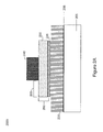
- FIG. 2A shows a cross-section diagram 2000 of the basic contact scheme using carbon nanotubes as the interfacial material.
- the substrate 205 may be sapphire, SiC, AlN or another material that is applicable for GaN technology with an additional film of semiconducting material 206 such as n-GaN.
- P-GaN 220 is deposited on top of substrate 205 .
- the additional film of semiconducting material 206 such as n-GaN forms a p-n junction with overlying p-GaN 220 material.
- substrate 205 should be understood to include overlying film of semiconducting material 206 like n-GaN.
- a fabric of CNTs 235 and metal 230 are contacting the p-GaN 220 with the CNTs interposed between the metal 230 and p-GaN 220 . Because the fabric of CNTs may be porous, both the metal and CNTs may be in contact with the p-GaN.
- the metal 230 and CNTs 235 comprise what is termed as the interface film 250 . The upper surface of the interface film is contacted by a metal bond pad 240 . An active region 260 is adjacent to the metal pad 240 .
- FIG. 2B shows an embodiment structure 2001 which is similar to structure 200 ; however, the interface film may have CNTs 235 on top of the metal 230 , making interface contact structure 250 ′.
- the metal is in intimate contact with the p-GaN.
- the primary role of the CNTs is to provide a transparent conductive film to enhance spreading current while inducing a minimal impact on optical transparency.
- the CNTs could assist in forming contact to the GaN if the metal 230 is sufficiently thin.
- a sufficiently thin metal may be 0.5 to 3 nm, for example.
- An active region 260 ′ is adjacent to the metal pad 240 .
- the interface layer 250 ′′ consists of multiple layers of CNT 235 ′ and metal 230 ′.
- the sequence of films may be: CNT-metal-CNT.
- a second example is: CNT-metal-CNT-metal.
- a third example is: metal-CNT-metal.
- the metal portion of the interface film may be etched away leaving primarily CNTs. Methods used to provide an active region in single layer embodiments are also employed in multilayered embodiments.
- the metal is etched before the nanotube fabric—because the CNT fabric is porous, the etchant will readily etch the multiple layers of metal—whether wet or dry.
- the CNT fabric can then be removed with a standard O 2 RIE to achieve the desired structure.
- the above embodiment portrays one variant of the interface layer labeled as 250 (also 250 ′ and 250 ′′) in FIG. 2A-C .
- the primary role of the interface layer is to provide good contact to the metal pad, good contact to the GaN and in some applications, allow for high optical transparency in the active contact region 260 (also 260 ′ and 260 ′′) adjacent to the metal pad.
- the role of the metal component of the interface layer may be as an etch-stop (for either RIE etch or wet etch) to define the metal pad 240 in FIG. 2A-C .
- An additional role of the metal may be to protect the CNTs from the device environment or from potentially damaging processing steps.
- FIGS. 3A-H displays a method of forming a high transmittance and low resistance contact to p-GaN by employing a CNT fabric as an interfacial layer. The steps for forming such a structure are listed below.
- substrate 305 like substrate 205 , includes an additional overlying film of semiconducting material 306 such as n-GaN, on which a p-GaN film 320 is deposited.
- substrate 305 will be understood to include additional overlying film of semiconducting material 306 .
- the use of semiconducting material 306 to form a p-n junction is well known in the art and will not be shown in the various embodiments that follow.
- Step 1 The process starting point is shown in FIG. 3A (structure 3000 ) depicting a substrate 305 , which is similar to substrate 205 presented in FIG. 2A-C .
- the p-GaN surface may be cleaned with an acid treatment (HF for example) prior to deposition of the CNTs to remove any protective oxides or other thin films.
- HF acid treatment
- FIG. 3B ( 3001 ) shows the substrate 305 and p-GaN film 320 with the first component of the interface structure deposited—the CNT fabric 335 .
- the CNTs may be deposited by spin-coating or spray-coating techniques, well known in the art.
- FIG. 3C ( 3002 ) depicts the application of an additional component of the interface structure 350 which is the metal film 330 .
- the metal contact/pad material 340 is then deposited on top of the interface structure 350 .
- FIG. 3D ( 3003 ) depicts the formation of the active area.
- Photoresist 370 is patterned on the bond pad metal layer 340 .
- the resist pattern is then transferred into the pad metal 340 either by a wet etch process or a reactive ion etch (RIE) process. This pattern defines the electrically active contact area of the GaN LED structure.
- RIE reactive ion etch
- Step 5 The pattern of structure 3003 is transferred to the interface layer 350 by either wet etching or dry etching metal 330 and then dry etching CNT fabric 335 , forming structure 3004 , depicted in FIG. 3E .
- the dry etching processing of CNT fabric 335 has been previously described in U.S. patent application Ser. No. 09/915,093, filed on Jul. 25, 2001, now U.S. Pat. No. 6,919,592, entitled ELECTROMECHANICAL MEMORY ARRAY USING NANOTUBE RIBBONS AND METHOD FOR MAKING SAME; U.S. patent application Ser. No. 10/850,100, filed on May 20, 2004, now U.S. Pat. No.
- FIG. 3F depicts a second patterning step by using photoresist 370 ′, which is patterned on the metal pad 340 .
- This photoresist pattern is used to define the metal bond pad that will make contact to appropriate electrical interconnects (not shown).
- Step 7 In FIG. 3G ( 3006 ), the photoresist pattern 370 ′ is transferred to the metal pad 340 by wet etch or RIE. RIE should only be used if the uppermost film 330 of the interface layer 350 is metal of sufficient thickness (>10 nm depending on continuity of thin film) so as to protect the CNTs from plasma damage.
- FIG. 3H shows the final structure 3007 with a preferred embodiment optional step in which the metal 330 of the interface film 350 may be wet etched, leaving only the CNTs fabric 335 in the region adjacent to the metal pad 340 .
- This step can be implemented to maximize transparency in the active region adjacent to the pad.
- metal 330 The main goal of metal 330 is to provide a low resistance contact between bond pad metal 340 and CNT fabric 335 . Most metals form a Schottky barrier contact to CNTs; however, some metals such as Ti and Pd form a nearly ohmic contact to a CNT fabric, which is ideal for this invention. Therefore, the main purpose of metal 330 is to provide an low resistance contact to CNT fabric 335 and to provide an additional ohmic contact to metal bond pad 340 . Ideally, the metal film 330 should be removed from the active region ( 360 and 360 ′ of FIG. 3H ) above the CNT fabric 335 .
- ultra-thin films ( ⁇ 10 nm) of metal 330 should be employed so that optical transmission is not degraded.
- a thin layer e.g. Pt
- Pt may be used to improve the resistance of the CNT fabric.
- FIGS. 4A and 4B show FESEM images of a completed GaN device fabricated using the above process flow.
- FIG. 4A shows the aluminum pad (dark disk) on the active CNT area (square).
- FIG. 4B shows a high magnification image of the edge of the aluminum pad and the CNTs adjacent to it.
- This device was made using GaN wafers obtained from CREE, Inc., consisting of a p-GaN/n-GaN heterojunction on a SiC substrate and a protective oxide layer.
- the backside of the wafer was coated with Shipley 1805 photoresist to protect the backside of the wafer during the stripping of the oxide.
- the wafer was then immersed in a buffered oxide etch to strip the oxide exposing a clean p-GaN surface.
- CNTs were then spun onto the wafer repeatedly until the resistance as measured by a 4-point-probe was about 100 ⁇ .
- the wafer was then annealed in vacuum at 300° C. for 30 minutes in order to promote adhesion of the CNT fabric and remove residual solvent.
- a metal bi-layer film of 4 nm of Ti and 150 nm of Al were then deposited on top of the CNT fabric by electron beam evaporation.
- the CNTs and the 4 nm of Ti comprise the interface layer 350 mentioned in FIG. 3
- the 150 nm of Al comprise the contact pad layer 340 .
- the photoresist was stripped in Shipley 1165 (1-methyl-2-pyrrolidinone or NMP) at a temperature of 80° C. The wafer was then rinsed in isopropyl alcohol and dried to neutralize and remove residual NMP.
- the wafer was then etched in RIE for 2 min in oxygen plasma at 200 W. After the etch process, the wafer was measured in the 4-point-probe, yielding an infinite resistance and indicating that the regions between the contacts are electrically nullified.
- the wafer was then spun with Shipley 1805 photoresist and patterned by exposing and developing as above. This process matches FIG. 3F . Similar to above, the photoresist was developed in MF-321 developer and the aluminum was allowed to etch resulting in the structure shown in FIG. 3G . The wafer was rinsed in DI and dried.
- the wafer was then immersed in an HCl-based Ti etchant for 25 sec in order to remove the 4 nm of Ti in the active region adjacent to the pad ( 360 and 360 ′ in FIG. 3H ).
- the wafer was rinsed in DI and dried.
- FIGS. 4A-B shows FESEM micrographs of the final structure.
- This structure was electrically tested, providing the Current-Voltage (I-V) curve shown in FIG. 5 .
- the aluminum pad of a device was wire-bonded with an aluminum wire. Contact was also made to the bottom of the substrate on which gold traces were located; thereby, making contact to the n-doped side of the junction. The voltage bias was applied between the pad and the substrate to produce this curve. Visible light emission was observed at the onset of the ON-current of the diode at approximately 3 V.
- a top-down optical image of the device during operation is shown in FIG. 6 . In this figure, light is emitting from the square region which is the active area contacted by CNTs. The shadowed dot in the center is the aluminum pad. One can also notice the shadow of the aluminum bond wire to the right of the pad.
- the bond pad metal 740 forms a low resistance contact to the CNT fabric 735 and will connect to outside electrical connections (not shown).
- P-GaN film 720 , interface layer 750 , active areas 760 , 760 ′ and substrate 705 are selected and constructed as in other embodiments.
- the substrates used in the experiment described in this example were films p-GaN on sapphire (alumina) substrates which had gold contacts on the bottom side of the wafer and came with a protective sputtered SiO 2 layer on the p-GaN layer to protect the film from corrosion, oxidation and damage.
- the samples were obtained from CREE Inc.
- FIG. 8 The resulting structure is shown in the FIG. 8 in which one can see the circular Al pad ( 801 ), the square CNT region ( 802 ) and the surface of the substrate.
- FIG. 9 shows microscope images of the light output from several such devices.
- FIG. 10 shows a current voltage characteristic of the CNT-contacted p-GaN device. The pathway of electric current is from the carbon-nanotube contact, down through the p-n junction and out through the lower contact of the substrate.
- a sacrificial material such as, but not limited to, alumina, Ge or a bi-layer alumina/Ge thin film is used to pattern the active region of the CNT fabric. Therefore, after patterning film 330 and CNT fabric 335 ( FIG. 3E ) a wet etch is performed to remove thin film 330 , leaving only the CNT fabric 335 . A second thin film 340 would then be deposited and patterned to make electrical contact to the CNT fabric.
- the CNT fabric layers may be a monolayer or multilayer fabric, which is deposited by means of spin-coating or spray-coating.
- the CNT solution may be aqueous or solvent based.
- the CNTs may be single-walled (SWNTs), multi-walled (MWNTs), or bundles thereof.
- the CNTs may be fabricated by any means including: Chemical vapor deposition (CVD), laser ablation technique or electric arc furnace.
- the patterning and electrical contacting of a CNT fabric on top of a semiconductor material is not limited to p-GaN.
- Other important Group V, III-V or II-VI substrates that may be of interest include, but are not limited to, diamond, Silicon, GaAs, AlN, AlGaN, GaP, SiC, InP and any combination of the materials Al, N, Ga, In, P, As, etc that would be used to form an optical emitting device.
- an anneal can be performed on the final structure to lower the contact resistance between the bond pad, CNT fabric and p-GaN substrate.
- This anneal may be a vacuum anneal, a forming gas anneal (4% H 2 in N 2 ) or a Rapid Thermal Anneal at various temperatures, depending on the metals used for the bond pad contact.
- the application of purified nanotubes is preferable.
- using proper bulk nanotube preparations which contain primarily metallic or semiconducting nanotubes would allow application of a nanotube fabric to a substrate.
- the application of single-walled, multiwalled or mixtures of such nanotubes can be envisioned with subsequent patterning and etching to generate desired structures.
- Certain embodiments involve controlled composition of carbon nanotube fabrics. Specifically, methods may be employed to control the relative amount of metallic and semiconducting nanotubes in the nanofabric to achieve the desired characteristics and make an appropriate contact to the GaN and metal bond pads. In this fashion, the nanofabric may be made to have a higher or lower percentage of metallic nanotubes relative to semiconducting nanotubes. Correspondingly, other properties of the nanofabric (e.g., resistance) will change. Further, in some embodiments it may be preferable to separate metallic nanotubes from semiconducting nanotubes, first applying a semiconducting nanotube layer to make contact to the GaN, followed by a metallic layer to make contact to the metal bond pads.
Abstract
Description
(e) Strip PR using NMP: NMP solvent at 80 C was used to strip the photoresist.
(f) RIE through Ti/CNTs to render electrically inactive (Al is the hardmask): A reactive ion etch step is used to etch away the CNTs in the areas not protected by the Al. The parameters used: 60 Watts, 25 sccm flow of O2, 20 mT pressure, 60 sec time.
(g) Pattern photoresist to define the metal pad wet etch Al using TMAH: A second photo patterning step is done to define a 100 nm diameter circular pad centered within the square region of metal. As done earlier, the TMAH developed is allowed to develop the resist and etch the Al.
(h) Strip the Ti using Ti etchant: A Ti chemical etch is used to remove the Ti film that is exposed outside of the circular pad region.
(i) Hot NMP to strip photoresist: NMP solvent at 80 C is used to strip the photoresist.
-
- U.S. patent application Ser. No. 09/915,093, filed on Jul. 25, 2001, now U.S. Pat. No. 6,919,592, entitled ELECTROMECHANICAL MEMORY ARRAY USING NANOTUBE RIBBONS AND METHOD FOR MAKING SAME;
- U.S. patent application Ser. No. 10/850,100, filed on May 20, 2004, now U.S. Pat. No. 7,056,758, entitled ELECTROMECHANICAL MEMORY ARRAY USING NANOTUBE RIBBONS AND METHOD FOR MAKING SAME;
- U.S. patent application Ser. No. 10/852,880, filed on May 25, 2004, entitled ELECTROMECHANICAL MEMORY ARRAY USING NANOTUBE RIBBONS AND METHOD FOR MAKING SAME;
- U.S. patent application Ser. No. 09/915,173, filed on Jul. 25, 2001, now U.S. Pat. No. 6,643,165, entitled ELECTROMECHANICAL MEMORY HAVING CELL SELECTION CIRCUITRY CONSTRUCTED WITH NANOTUBE TECHNOLOGY;
- U.S. patent application Ser. No. 10/693,241, filed on Oct. 24, 2003, now U.S. Pat. No. 7,120,047, entitled DEVICE SELECTION CIRCUITRY CONSTRUCTED WITH NANOTUBE TECHNOLOGY;
- U.S. patent application Ser. No. 09/915,095, filed on Jul. 25, 2001, now U.S. Pat. No. 6,574,130, entitled HYBRID CIRCUIT HAVING NANOTUBE ELECTROMECHANICAL MEMORY;
- U.S. patent application Ser. No. 10/379,973, filed on Mar. 5, 2003, now U.S. Pat. No. 6,836,424, entitled HYBRID CIRCUIT HAVING NANOTUBE ELECTROMECHANICAL MEMORY;
- U.S. patent application Ser. No. 10/964,150, filed on Oct. 13, 2004, entitled HYBRID CIRCUIT HAVING NANOTUBE ELECTROMECHANICAL MEMORY;
- U.S. patent application Ser. No. 10/033,323, filed on Dec. 28, 2001, now U.S. Pat. No. 6,911,682, entitled ELECTROMECHANICAL THREE-TRACE JUNCTION DEVICES;
- U.S. patent application Ser. No. 10/802,900, filed on Mar. 17, 2004, entitled ELECTROMECHANICAL THREE-TRACE JUNCTION DEVICES;
- U.S. patent application Ser. No. 10/033,032, filed on Dec. 28, 2001, now U.S. Pat. No. 6,784,028, entitled METHODS OF MAKING ELECTROMECHANICAL THREE-TRACE JUNCTION DEVICES;
- U.S. patent application Ser. No. 10/824,679, filed on Apr. 15, 2004, now U.S. Pat. No. 6,979,590, entitled METHODS OF MAKING ELECTROMECHANICAL THREE-TRACE JUNCTION DEVICES;
- U.S. patent application Ser. No. 11/188,678, filed on Jul. 25, 2005, entitled METHODS OF MAKING ELECTROMECHANICAL THREE-TRACE JUNCTION DEVICES;
- U.S. patent application Ser. No. 10/128,118, filed on Apr. 23, 2002, now U.S. Pat. No. 6,706,402, entitled NANOTUBE FILMS AND ARTICLES;
- U.S. patent application Ser. No. 10/774,682, filed on Feb. 9, 2004, entitled NANOTUBE FILMS AND ARTICLES;
- U.S. patent application Ser. No. 10/776,573, filed on Feb. 11, 2004, now U.S. Pat. No. 6,942,921, entitled NANOTUBE FILMS AND ARTICLES;
- U.S. patent application Ser. No. 11/111,582, filed on Apr. 21, 2005, entitled NANOTUBE FILMS AND ARTICLES;
- U.S. patent application Ser. No. 10/128,117, filed on Apr. 23, 2002, now U.S. Pat. No. 6,835,591, entitled METHODS OF NANOTUBE FILMS AND ARTICLES;
- U.S. patent application Ser. No. 11/007,752, filed on Dec. 8, 2004, entitled METHODS OF NANOTUBE FILMS AND ARTICLES;
- U.S. patent application Ser. No. 11/010,491, filed on Dec. 13, 2004, entitled METHODS OF NANOTUBE FILMS AND ARTICLES;
- U.S. patent application Ser. No. 10/776,059, filed on Feb. 11, 2004, entitled METHODS OF USING PRE-FORMED NANOTUBES TO MAKE CARBON NANOTUBE FILMS, LAYERS, FABRICS, RIBBONS, ELEMENTS AND ARTICLES (HORIZONTAL), now U.S. Patent Publication 2004/0181630;
- U.S. patent application Ser. No. 11/193,795, filed on Jul. 29, 2005, entitled METHODS OF USING PRE-FORMED NANOTUBES TO MAKE CARBON NANOTUBE FILMS, LAYERS, FABRICS, RIBBONS, ELEMENTS AND ARTICLES (HORIZONTAL);
- U.S. patent application Ser. No. 10/341,005, filed on Jan. 13, 2003, entitled METHODS OF MAKING CARBON NANOTUBE FILMS, LAYERS, FABRICS, RIBBONS, ELEMENTS AND ARTICLES; and,
- U.S. patent application Ser. No. 10/341,130, filed on Jan. 13, 2003, entitled CARBON NANOTUBE FILMS, LAYERS, FABRICS, RIBBONS, ELEMENTS AND ARTICLES.
Claims (13)
Priority Applications (1)
| Application Number | Priority Date | Filing Date | Title |
|---|---|---|---|
| US12/506,878 US8044388B2 (en) | 2001-07-25 | 2009-07-21 | Method of forming a carbon nanotube-based contact to semiconductor |
Applications Claiming Priority (9)
| Application Number | Priority Date | Filing Date | Title |
|---|---|---|---|
| US09/915,173 US6643165B2 (en) | 2001-07-25 | 2001-07-25 | Electromechanical memory having cell selection circuitry constructed with nanotube technology |
| US09/915,093 US6919592B2 (en) | 2001-07-25 | 2001-07-25 | Electromechanical memory array using nanotube ribbons and method for making same |
| US09/915,095 US6574130B2 (en) | 2001-07-25 | 2001-07-25 | Hybrid circuit having nanotube electromechanical memory |
| US10/128,118 US6706402B2 (en) | 2001-07-25 | 2002-04-23 | Nanotube films and articles |
| US10/776,573 US6942921B2 (en) | 2001-07-25 | 2004-02-11 | Nanotube films and articles |
| US11/111,582 US20050191495A1 (en) | 2001-07-25 | 2005-04-21 | Nanotube films and articles |
| US77546106P | 2006-02-21 | 2006-02-21 | |
| US11/708,929 US7563711B1 (en) | 2001-07-25 | 2007-02-21 | Method of forming a carbon nanotube-based contact to semiconductor |
| US12/506,878 US8044388B2 (en) | 2001-07-25 | 2009-07-21 | Method of forming a carbon nanotube-based contact to semiconductor |
Related Parent Applications (1)
| Application Number | Title | Priority Date | Filing Date |
|---|---|---|---|
| US11/708,929 Continuation US7563711B1 (en) | 2001-07-25 | 2007-02-21 | Method of forming a carbon nanotube-based contact to semiconductor |
Publications (2)
| Publication Number | Publication Date |
|---|---|
| US20100148183A1 US20100148183A1 (en) | 2010-06-17 |
| US8044388B2 true US8044388B2 (en) | 2011-10-25 |
Family
ID=39766318
Family Applications (2)
| Application Number | Title | Priority Date | Filing Date |
|---|---|---|---|
| US11/708,929 Expired - Lifetime US7563711B1 (en) | 2001-07-25 | 2007-02-21 | Method of forming a carbon nanotube-based contact to semiconductor |
| US12/506,878 Expired - Fee Related US8044388B2 (en) | 2001-07-25 | 2009-07-21 | Method of forming a carbon nanotube-based contact to semiconductor |
Family Applications Before (1)
| Application Number | Title | Priority Date | Filing Date |
|---|---|---|---|
| US11/708,929 Expired - Lifetime US7563711B1 (en) | 2001-07-25 | 2007-02-21 | Method of forming a carbon nanotube-based contact to semiconductor |
Country Status (3)
| Country | Link |
|---|---|
| US (2) | US7563711B1 (en) |
| TW (1) | TWI421918B (en) |
| WO (1) | WO2008115652A1 (en) |
Cited By (1)
| Publication number | Priority date | Publication date | Assignee | Title |
|---|---|---|---|---|
| US20140339592A1 (en) * | 2011-04-29 | 2014-11-20 | Tsinghua University | Light emitting diode |
Families Citing this family (21)
| Publication number | Priority date | Publication date | Assignee | Title |
|---|---|---|---|---|
| US7563711B1 (en) | 2001-07-25 | 2009-07-21 | Nantero, Inc. | Method of forming a carbon nanotube-based contact to semiconductor |
| KR100790216B1 (en) | 2006-10-17 | 2008-01-02 | 삼성전자주식회사 | A transparent cnt electrode using conductive dispersant and preparation method thereof |
| KR100883737B1 (en) * | 2007-01-17 | 2009-02-12 | 삼성전자주식회사 | Transparent carbon nanotube electrode with net shape carbon nanotube film and preparation method thereof |
| EP2204074B1 (en) | 2007-09-10 | 2019-11-06 | University of Florida Research Foundation, Inc. | Nanotube enabled, gate-voltage controlled light emitting diodes |
| US20110163298A1 (en) * | 2010-01-04 | 2011-07-07 | Chien-Min Sung | Graphene and Hexagonal Boron Nitride Devices |
| US8507966B2 (en) | 2010-03-02 | 2013-08-13 | Micron Technology, Inc. | Semiconductor cells, arrays, devices and systems having a buried conductive line and methods for forming the same |
| US20110227043A1 (en) | 2010-03-19 | 2011-09-22 | International Business Machines Corporation | Graphene sensor |
| KR101072193B1 (en) * | 2010-04-01 | 2011-10-10 | 엘지이노텍 주식회사 | Light emitting device, fabrication method thereof, and light emitting device package |
| KR20120003775A (en) * | 2010-07-05 | 2012-01-11 | 엘지이노텍 주식회사 | Light emitting device and method for fabricating the same, light emitting device package, and lighting system |
| US9018734B2 (en) * | 2011-04-15 | 2015-04-28 | The United States Of America As Represented By The Secretary Of The Army | Single wall carbon nanotube diodes |
| ES2592530T3 (en) | 2011-06-17 | 2016-11-30 | Fiberweb, Llc | Multi-layer vapor permeable article, substantially waterproof |
| US10369769B2 (en) | 2011-06-23 | 2019-08-06 | Fiberweb, Inc. | Vapor-permeable, substantially water-impermeable multilayer article |
| WO2012177996A2 (en) | 2011-06-23 | 2012-12-27 | Fiberweb, Inc. | Vapor permeable, substantially water impermeable multilayer article |
| WO2012178011A2 (en) | 2011-06-24 | 2012-12-27 | Fiberweb, Inc. | Vapor-permeable, substantially water-impermeable multilayer article |
| CN103367554B (en) * | 2012-03-28 | 2016-03-30 | 清华大学 | The preparation method of light-emitting diode |
| CN104769661B (en) | 2012-11-05 | 2017-07-18 | 佛罗里达大学研究基金会有限公司 | Luminance compensation in display |
| CN107293591B (en) | 2016-04-11 | 2020-03-31 | 华邦电子股份有限公司 | Printed circuit, thin film transistor and manufacturing method thereof |
| TWI601454B (en) * | 2016-04-11 | 2017-10-01 | 華邦電子股份有限公司 | Printed circuit, thin film transistor and manufacturing method thereof |
| US10349834B2 (en) * | 2016-12-30 | 2019-07-16 | Palo Alto Research Center Incorporated | Sensing health using fluid sensors in feminine hygiene products |
| US10485476B2 (en) * | 2016-12-30 | 2019-11-26 | Palo Alto Research Center Incorporated | Chromatography-aided substance sensing in absorbent hygiene and medical products |
| US10985164B1 (en) * | 2019-09-27 | 2021-04-20 | Nanya Technology Corporation | Semiconductor device with nanowire contact and method for fabricating the same |
Citations (37)
| Publication number | Priority date | Publication date | Assignee | Title |
|---|---|---|---|---|
| US4979149A (en) | 1986-09-10 | 1990-12-18 | Lgz Landis & Gyr Zug Ag | Non-volatile memory device including a micro-mechanical storage element |
| WO2000048195A1 (en) | 1999-02-12 | 2000-08-17 | Board Of Trustees Operating Michigan State University | Nanocapsules containing charged particles, their uses and methods of forming the same |
| WO2002045113A1 (en) | 2000-11-29 | 2002-06-06 | Nec Corporation | Pattern forming method for carbon nanotube, and field emission cold cathode and method of manufacturing the cold cathode |
| US6409567B1 (en) | 1997-12-15 | 2002-06-25 | E.I. Du Pont De Nemours And Company | Past-deposited carbon electron emitters |
| US6417525B1 (en) | 1997-03-19 | 2002-07-09 | Sharp Kabushiki Kaisha | Semiconductor light emitter with current block region formed over the semiconductor layer and electrode connection portion for connecting the pad electrode to the translucent electrode |
| US6423583B1 (en) | 2001-01-03 | 2002-07-23 | International Business Machines Corporation | Methodology for electrically induced selective breakdown of nanotubes |
| US6426687B1 (en) | 2001-05-22 | 2002-07-30 | The Aerospace Corporation | RF MEMS switch |
| US6445006B1 (en) * | 1995-12-20 | 2002-09-03 | Advanced Technology Materials, Inc. | Microelectronic and microelectromechanical devices comprising carbon nanotube components, and methods of making same |
| US6443901B1 (en) | 2000-06-15 | 2002-09-03 | Koninklijke Philips Electronics N.V. | Capacitive micromachined ultrasonic transducers |
| US6504292B1 (en) * | 1999-07-15 | 2003-01-07 | Agere Systems Inc. | Field emitting device comprising metallized nanostructures and method for making the same |
| US6548841B2 (en) | 2000-11-09 | 2003-04-15 | Texas Instruments Incorporated | Nanomechanical switches and circuits |
| US6574130B2 (en) | 2001-07-25 | 2003-06-03 | Nantero, Inc. | Hybrid circuit having nanotube electromechanical memory |
| US6643165B2 (en) | 2001-07-25 | 2003-11-04 | Nantero, Inc. | Electromechanical memory having cell selection circuitry constructed with nanotube technology |
| US20040031975A1 (en) | 2002-03-18 | 2004-02-19 | Max-Planck-Gesellschaft Zur Forderung Der Wissenschaften E.V., A German Corporation | Field effect transistor memory cell, memory device and method for manufacturing a field effect transistor memory cell |
| US6784028B2 (en) | 2001-12-28 | 2004-08-31 | Nantero, Inc. | Methods of making electromechanical three-trace junction devices |
| US20040181630A1 (en) | 2001-07-25 | 2004-09-16 | Nantero, Inc. | Devices having horizontally-disposed nanofabric articles and methods of making the same |
| US6803840B2 (en) | 2001-03-30 | 2004-10-12 | California Institute Of Technology | Pattern-aligned carbon nanotube growth and tunable resonator apparatus |
| US6809462B2 (en) | 2000-04-05 | 2004-10-26 | Sri International | Electroactive polymer sensors |
| US20040232429A1 (en) | 1997-05-08 | 2004-11-25 | Showa Denko K.K. | Electrode for light-emitting semiconductor devices and method of producing the electrode |
| US20040238907A1 (en) | 2003-06-02 | 2004-12-02 | Pinkerton Joseph F. | Nanoelectromechanical transistors and switch systems |
| US6835591B2 (en) | 2001-07-25 | 2004-12-28 | Nantero, Inc. | Methods of nanotube films and articles |
| US20050068128A1 (en) | 2003-06-20 | 2005-03-31 | David Yip | Anchorless electrostatically activated micro electromechanical system switch |
| US6891320B2 (en) * | 2000-11-17 | 2005-05-10 | Kabushiki Kaisha Toshiba | Field emission cold cathode device of lateral type |
| US6911682B2 (en) | 2001-12-28 | 2005-06-28 | Nantero, Inc. | Electromechanical three-trace junction devices |
| US20050191495A1 (en) | 2001-07-25 | 2005-09-01 | Nantero, Inc. | Nanotube films and articles |
| WO2005083751A2 (en) | 2004-02-20 | 2005-09-09 | University Of Florida Research Foundation, Inc. | Semiconductor device and method using nanotube contacts |
| US20050218523A1 (en) | 2004-03-30 | 2005-10-06 | Dubin Valery M | Integrated circuit with metal layer having carbon nanotubes and methods of making same |
| US6955937B1 (en) | 2004-08-12 | 2005-10-18 | Lsi Logic Corporation | Carbon nanotube memory cell for integrated circuit structure with removable side spacers to permit access to memory cell and process for forming such memory cell |
| US20050230763A1 (en) | 2004-04-15 | 2005-10-20 | Taiwan Semiconductor Manufacturing Co., Ltd. | Method of manufacturing a microelectronic device with electrode perturbing sill |
| US6969651B1 (en) | 2004-03-26 | 2005-11-29 | Lsi Logic Corporation | Layout design and process to form nanotube cell for nanotube memory applications |
| US20050266605A1 (en) | 2004-06-01 | 2005-12-01 | Canon Kabushiki Kaisha | Process for patterning nanocarbon material, semiconductor device, and method for manufacturing semiconductor device |
| US6975189B1 (en) | 2000-11-02 | 2005-12-13 | Telasic Communications, Inc. | On-chip multilayer metal shielded transmission line |
| US7056758B2 (en) | 2001-07-25 | 2006-06-06 | Nantero, Inc. | Electromechanical memory array using nanotube ribbons and method for making same |
| US20060237537A1 (en) | 2002-09-30 | 2006-10-26 | Nanosys, Inc. | Applications of nano-enabled large area macroelectronic substrates incorporating nanowires and nanowire composites |
| US7176505B2 (en) | 2001-12-28 | 2007-02-13 | Nantero, Inc. | Electromechanical three-trace junction devices |
| WO2008115652A1 (en) | 2007-02-21 | 2008-09-25 | Nantero, Inc. | Method of forming a carbon nanotube-based contact to semiconductor |
| US7566478B2 (en) | 2001-07-25 | 2009-07-28 | Nantero, Inc. | Methods of making carbon nanotube films, layers, fabrics, ribbons, elements and articles |
Family Cites Families (64)
| Publication number | Priority date | Publication date | Assignee | Title |
|---|---|---|---|---|
| US6100109A (en) * | 1994-11-02 | 2000-08-08 | Siemens Aktiengesellschaft | Method for producing a memory device |
| US6057637A (en) * | 1996-09-13 | 2000-05-02 | The Regents Of The University Of California | Field emission electron source |
| AU6545698A (en) | 1997-03-07 | 1998-09-22 | William Marsh Rice University | Carbon fibers formed from single-wall carbon nanotubes |
| JP3902883B2 (en) * | 1998-03-27 | 2007-04-11 | キヤノン株式会社 | Nanostructure and manufacturing method thereof |
| JP2002518280A (en) | 1998-06-19 | 2002-06-25 | ザ・リサーチ・ファウンデーション・オブ・ステイト・ユニバーシティ・オブ・ニューヨーク | Aligned free-standing carbon nanotubes and their synthesis |
| US6346189B1 (en) * | 1998-08-14 | 2002-02-12 | The Board Of Trustees Of The Leland Stanford Junior University | Carbon nanotube structures made using catalyst islands |
| US6630772B1 (en) * | 1998-09-21 | 2003-10-07 | Agere Systems Inc. | Device comprising carbon nanotube field emitter structure and process for forming device |
| JP3943272B2 (en) | 1999-01-18 | 2007-07-11 | 双葉電子工業株式会社 | Film forming method of carbon nanotube |
| US6250984B1 (en) * | 1999-01-25 | 2001-06-26 | Agere Systems Guardian Corp. | Article comprising enhanced nanotube emitter structure and process for fabricating article |
| US6256767B1 (en) * | 1999-03-29 | 2001-07-03 | Hewlett-Packard Company | Demultiplexer for a molecular wire crossbar network (MWCN DEMUX) |
| US6128214A (en) * | 1999-03-29 | 2000-10-03 | Hewlett-Packard | Molecular wire crossbar memory |
| US6314019B1 (en) * | 1999-03-29 | 2001-11-06 | Hewlett-Packard Company | Molecular-wire crossbar interconnect (MWCI) for signal routing and communications |
| AUPP976499A0 (en) * | 1999-04-16 | 1999-05-06 | Commonwealth Scientific And Industrial Research Organisation | Multilayer carbon nanotube films |
| AU782000B2 (en) | 1999-07-02 | 2005-06-23 | President And Fellows Of Harvard College | Nanoscopic wire-based devices, arrays, and methods of their manufacture |
| JP4063451B2 (en) | 1999-07-26 | 2008-03-19 | 双葉電子工業株式会社 | Carbon nanotube pattern formation method |
| US6277318B1 (en) * | 1999-08-18 | 2001-08-21 | Agere Systems Guardian Corp. | Method for fabrication of patterned carbon nanotube films |
| KR20010055501A (en) * | 1999-12-10 | 2001-07-04 | 김순택 | Method for forming cathode of field emission display |
| KR20010056153A (en) * | 1999-12-14 | 2001-07-04 | 구자홍 | Field emission display device and its fabrication method |
| US6495116B1 (en) * | 2000-04-10 | 2002-12-17 | Lockheed Martin Corporation | Net shape manufacturing using carbon nanotubes |
| JP4222757B2 (en) * | 2000-05-04 | 2009-02-12 | クナノ・アーベー | Nanostructure |
| EP1170799A3 (en) * | 2000-07-04 | 2009-04-01 | Infineon Technologies AG | Electronic device and method of manufacture of an electronic device |
| JP3859199B2 (en) | 2000-07-18 | 2006-12-20 | エルジー エレクトロニクス インコーポレイティド | Carbon nanotube horizontal growth method and field effect transistor using the same |
| KR100376768B1 (en) * | 2000-08-23 | 2003-03-19 | 한국과학기술연구원 | Parallel and selective growth and connection method of carbon nanotubes on the substrates for electronic-spintronic device applications |
| US6495258B1 (en) * | 2000-09-20 | 2002-12-17 | Auburn University | Structures with high number density of carbon nanotubes and 3-dimensional distribution |
| AU2904602A (en) | 2000-12-11 | 2002-06-24 | Harvard College | Nanosensors |
| AU2002254367B2 (en) * | 2001-03-26 | 2007-12-06 | Eikos, Inc. | Coatings containing carbon nanotubes |
| US20020160111A1 (en) * | 2001-04-25 | 2002-10-31 | Yi Sun | Method for fabrication of field emission devices using carbon nanotube film as a cathode |
| US7157068B2 (en) * | 2001-05-21 | 2007-01-02 | The Trustees Of Boston College | Varied morphology carbon nanotubes and method for their manufacture |
| JP4207398B2 (en) * | 2001-05-21 | 2009-01-14 | 富士ゼロックス株式会社 | Method for manufacturing wiring of carbon nanotube structure, wiring of carbon nanotube structure, and carbon nanotube device using the same |
| US20040023253A1 (en) * | 2001-06-11 | 2004-02-05 | Sandeep Kunwar | Device structure for closely spaced electrodes |
| US6924538B2 (en) * | 2001-07-25 | 2005-08-02 | Nantero, Inc. | Devices having vertically-disposed nanofabric articles and methods of making the same |
| US7118693B2 (en) * | 2001-07-27 | 2006-10-10 | Eikos, Inc. | Conformal coatings comprising carbon nanotubes |
| WO2003011755A1 (en) * | 2001-07-27 | 2003-02-13 | University Of Surrey | Production of carbon nanotubes |
| KR100455284B1 (en) | 2001-08-14 | 2004-11-12 | 삼성전자주식회사 | High-throughput sensor for detecting biomolecules using carbon nanotubes |
| JP4306990B2 (en) | 2001-10-18 | 2009-08-05 | 独立行政法人産業技術総合研究所 | Nonlinear optical element |
| US6645628B2 (en) * | 2001-11-13 | 2003-11-11 | The United States Of America As Represented By The Secretary Of The Air Force | Carbon nanotube coated anode |
| US6894359B2 (en) * | 2002-09-04 | 2005-05-17 | Nanomix, Inc. | Sensitivity control for nanotube sensors |
| WO2003063208A2 (en) * | 2002-01-18 | 2003-07-31 | California Institute Of Technology | Array-based architecture for molecular electronics |
| JP2003243316A (en) * | 2002-02-20 | 2003-08-29 | Fuji Photo Film Co Ltd | Substrate for semiconductor element and its manufacturing method |
| US6889216B2 (en) * | 2002-03-12 | 2005-05-03 | Knowm Tech, Llc | Physical neural network design incorporating nanotechnology |
| US6858197B1 (en) * | 2002-03-13 | 2005-02-22 | The United States Of America As Represented By The Administrator Of The National Aeronautics And Space Administration | Controlled patterning and growth of single wall and multi-wall carbon nanotubes |
| US6919730B2 (en) * | 2002-03-18 | 2005-07-19 | Honeywell International, Inc. | Carbon nanotube sensor |
| US6899945B2 (en) * | 2002-03-19 | 2005-05-31 | William Marsh Rice University | Entangled single-wall carbon nanotube solid material and methods for making same |
| US6891227B2 (en) * | 2002-03-20 | 2005-05-10 | International Business Machines Corporation | Self-aligned nanotube field effect transistor and method of fabricating same |
| US6872645B2 (en) * | 2002-04-02 | 2005-03-29 | Nanosys, Inc. | Methods of positioning and/or orienting nanostructures |
| US6946410B2 (en) * | 2002-04-05 | 2005-09-20 | E. I. Du Pont De Nemours And Company | Method for providing nano-structures of uniform length |
| AU2003229333A1 (en) * | 2002-05-21 | 2003-12-12 | Eikos, Inc. | Method for patterning carbon nanotube coating and carbon nanotube wiring |
| US20040007528A1 (en) * | 2002-07-03 | 2004-01-15 | The Regents Of The University Of California | Intertwined, free-standing carbon nanotube mesh for use as separation, concentration, and/or filtration medium |
| JP4547852B2 (en) * | 2002-09-04 | 2010-09-22 | 富士ゼロックス株式会社 | Manufacturing method of electrical parts |
| US7052588B2 (en) * | 2002-11-27 | 2006-05-30 | Molecular Nanosystems, Inc. | Nanotube chemical sensor based on work function of electrodes |
| US20040265550A1 (en) * | 2002-12-06 | 2004-12-30 | Glatkowski Paul J. | Optically transparent nanostructured electrical conductors |
| US6919740B2 (en) * | 2003-01-31 | 2005-07-19 | Hewlett-Packard Development Company, Lp. | Molecular-junction-nanowire-crossbar-based inverter, latch, and flip-flop circuits, and more complex circuits composed, in part, from molecular-junction-nanowire-crossbar-based inverter, latch, and flip-flop circuits |
| US6918284B2 (en) * | 2003-03-24 | 2005-07-19 | The United States Of America As Represented By The Secretary Of The Navy | Interconnected networks of single-walled carbon nanotubes |
| US7537803B2 (en) * | 2003-04-08 | 2009-05-26 | New Jersey Institute Of Technology | Polymer coating/encapsulation of nanoparticles using a supercritical antisolvent process |
| US7780918B2 (en) * | 2003-05-14 | 2010-08-24 | Nantero, Inc. | Sensor platform using a horizontally oriented nanotube element |
| US7354877B2 (en) * | 2003-10-29 | 2008-04-08 | Lockheed Martin Corporation | Carbon nanotube fabrics |
| TWI228833B (en) * | 2004-05-04 | 2005-03-01 | Ind Tech Res Inst | Method for enhancing the electrical characteristics of organic electronic devices |
| TWI244159B (en) * | 2004-04-16 | 2005-11-21 | Ind Tech Res Inst | Metal nanoline process and its application on aligned growth of carbon nanotube or silicon nanowire |
| US20050233263A1 (en) * | 2004-04-20 | 2005-10-20 | Applied Materials, Inc. | Growth of carbon nanotubes at low temperature |
| JP2006080170A (en) * | 2004-09-08 | 2006-03-23 | Hitachi Cable Ltd | Manufacturing method of cnt-containing wiring material and target material for sputtering |
| JP4517865B2 (en) * | 2005-01-26 | 2010-08-04 | Jfeエンジニアリング株式会社 | Method for producing carbon nanotube electrode |
| US20060237799A1 (en) * | 2005-04-21 | 2006-10-26 | Lsi Logic Corporation | Carbon nanotube memory cells having flat bottom electrode contact surface |
| US7402770B2 (en) * | 2005-06-10 | 2008-07-22 | Lsi Logic Corporation | Nano structure electrode design |
| US7538040B2 (en) * | 2005-06-30 | 2009-05-26 | Nantero, Inc. | Techniques for precision pattern transfer of carbon nanotubes from photo mask to wafers |
-
2007
- 2007-02-21 US US11/708,929 patent/US7563711B1/en not_active Expired - Lifetime
-
2008
- 2008-02-20 WO PCT/US2008/054431 patent/WO2008115652A1/en active Application Filing
- 2008-02-21 TW TW97106049A patent/TWI421918B/en active
-
2009
- 2009-07-21 US US12/506,878 patent/US8044388B2/en not_active Expired - Fee Related
Patent Citations (49)
| Publication number | Priority date | Publication date | Assignee | Title |
|---|---|---|---|---|
| US4979149A (en) | 1986-09-10 | 1990-12-18 | Lgz Landis & Gyr Zug Ag | Non-volatile memory device including a micro-mechanical storage element |
| US6445006B1 (en) * | 1995-12-20 | 2002-09-03 | Advanced Technology Materials, Inc. | Microelectronic and microelectromechanical devices comprising carbon nanotube components, and methods of making same |
| US6417525B1 (en) | 1997-03-19 | 2002-07-09 | Sharp Kabushiki Kaisha | Semiconductor light emitter with current block region formed over the semiconductor layer and electrode connection portion for connecting the pad electrode to the translucent electrode |
| US20040232429A1 (en) | 1997-05-08 | 2004-11-25 | Showa Denko K.K. | Electrode for light-emitting semiconductor devices and method of producing the electrode |
| US6409567B1 (en) | 1997-12-15 | 2002-06-25 | E.I. Du Pont De Nemours And Company | Past-deposited carbon electron emitters |
| WO2000048195A1 (en) | 1999-02-12 | 2000-08-17 | Board Of Trustees Operating Michigan State University | Nanocapsules containing charged particles, their uses and methods of forming the same |
| US6504292B1 (en) * | 1999-07-15 | 2003-01-07 | Agere Systems Inc. | Field emitting device comprising metallized nanostructures and method for making the same |
| US6809462B2 (en) | 2000-04-05 | 2004-10-26 | Sri International | Electroactive polymer sensors |
| US6443901B1 (en) | 2000-06-15 | 2002-09-03 | Koninklijke Philips Electronics N.V. | Capacitive micromachined ultrasonic transducers |
| US6975189B1 (en) | 2000-11-02 | 2005-12-13 | Telasic Communications, Inc. | On-chip multilayer metal shielded transmission line |
| US6548841B2 (en) | 2000-11-09 | 2003-04-15 | Texas Instruments Incorporated | Nanomechanical switches and circuits |
| US6891320B2 (en) * | 2000-11-17 | 2005-05-10 | Kabushiki Kaisha Toshiba | Field emission cold cathode device of lateral type |
| WO2002045113A1 (en) | 2000-11-29 | 2002-06-06 | Nec Corporation | Pattern forming method for carbon nanotube, and field emission cold cathode and method of manufacturing the cold cathode |
| US6423583B1 (en) | 2001-01-03 | 2002-07-23 | International Business Machines Corporation | Methodology for electrically induced selective breakdown of nanotubes |
| US6803840B2 (en) | 2001-03-30 | 2004-10-12 | California Institute Of Technology | Pattern-aligned carbon nanotube growth and tunable resonator apparatus |
| US6426687B1 (en) | 2001-05-22 | 2002-07-30 | The Aerospace Corporation | RF MEMS switch |
| US7056758B2 (en) | 2001-07-25 | 2006-06-06 | Nantero, Inc. | Electromechanical memory array using nanotube ribbons and method for making same |
| US7298016B2 (en) | 2001-07-25 | 2007-11-20 | Nantero, Inc. | Electromechanical memory array using nanotube ribbons and method for making same |
| US7745810B2 (en) | 2001-07-25 | 2010-06-29 | Nantero, Inc. | Nanotube films and articles |
| US7566478B2 (en) | 2001-07-25 | 2009-07-28 | Nantero, Inc. | Methods of making carbon nanotube films, layers, fabrics, ribbons, elements and articles |
| US6835591B2 (en) | 2001-07-25 | 2004-12-28 | Nantero, Inc. | Methods of nanotube films and articles |
| US6836424B2 (en) | 2001-07-25 | 2004-12-28 | Nantero, Inc. | Hybrid circuit having nanotube electromechanical memory |
| US7342818B2 (en) | 2001-07-25 | 2008-03-11 | Nantero, Inc. | Hybrid circuit having nanotube electromechanical memory |
| US7335528B2 (en) | 2001-07-25 | 2008-02-26 | Nantero, Inc. | Methods of nanotube films and articles |
| US7304357B2 (en) | 2001-07-25 | 2007-12-04 | Nantero, Inc. | Devices having horizontally-disposed nanofabric articles and methods of making the same |
| US20050191495A1 (en) | 2001-07-25 | 2005-09-01 | Nantero, Inc. | Nanotube films and articles |
| US20040181630A1 (en) | 2001-07-25 | 2004-09-16 | Nantero, Inc. | Devices having horizontally-disposed nanofabric articles and methods of making the same |
| US6942921B2 (en) | 2001-07-25 | 2005-09-13 | Nantero, Inc. | Nanotube films and articles |
| US7264990B2 (en) | 2001-07-25 | 2007-09-04 | Nantero, Inc. | Methods of nanotubes films and articles |
| US7120047B2 (en) | 2001-07-25 | 2006-10-10 | Segal Brent M | Device selection circuitry constructed with nanotube technology |
| US6574130B2 (en) | 2001-07-25 | 2003-06-03 | Nantero, Inc. | Hybrid circuit having nanotube electromechanical memory |
| US6643165B2 (en) | 2001-07-25 | 2003-11-04 | Nantero, Inc. | Electromechanical memory having cell selection circuitry constructed with nanotube technology |
| US6911682B2 (en) | 2001-12-28 | 2005-06-28 | Nantero, Inc. | Electromechanical three-trace junction devices |
| US6784028B2 (en) | 2001-12-28 | 2004-08-31 | Nantero, Inc. | Methods of making electromechanical three-trace junction devices |
| US6979590B2 (en) | 2001-12-28 | 2005-12-27 | Nantero, Inc. | Methods of making electromechanical three-trace junction devices |
| US7419845B2 (en) | 2001-12-28 | 2008-09-02 | Nantero, Inc. | Methods of making electromechanical three-trace junction devices |
| US7176505B2 (en) | 2001-12-28 | 2007-02-13 | Nantero, Inc. | Electromechanical three-trace junction devices |
| US20040031975A1 (en) | 2002-03-18 | 2004-02-19 | Max-Planck-Gesellschaft Zur Forderung Der Wissenschaften E.V., A German Corporation | Field effect transistor memory cell, memory device and method for manufacturing a field effect transistor memory cell |
| US20060237537A1 (en) | 2002-09-30 | 2006-10-26 | Nanosys, Inc. | Applications of nano-enabled large area macroelectronic substrates incorporating nanowires and nanowire composites |
| US20040238907A1 (en) | 2003-06-02 | 2004-12-02 | Pinkerton Joseph F. | Nanoelectromechanical transistors and switch systems |
| US20050068128A1 (en) | 2003-06-20 | 2005-03-31 | David Yip | Anchorless electrostatically activated micro electromechanical system switch |
| US20050199894A1 (en) | 2004-02-20 | 2005-09-15 | University Of Florida Research Foundation, Inc. | Semiconductor device and method using nanotube contacts |
| WO2005083751A2 (en) | 2004-02-20 | 2005-09-09 | University Of Florida Research Foundation, Inc. | Semiconductor device and method using nanotube contacts |
| US6969651B1 (en) | 2004-03-26 | 2005-11-29 | Lsi Logic Corporation | Layout design and process to form nanotube cell for nanotube memory applications |
| US20050218523A1 (en) | 2004-03-30 | 2005-10-06 | Dubin Valery M | Integrated circuit with metal layer having carbon nanotubes and methods of making same |
| US20050230763A1 (en) | 2004-04-15 | 2005-10-20 | Taiwan Semiconductor Manufacturing Co., Ltd. | Method of manufacturing a microelectronic device with electrode perturbing sill |
| US20050266605A1 (en) | 2004-06-01 | 2005-12-01 | Canon Kabushiki Kaisha | Process for patterning nanocarbon material, semiconductor device, and method for manufacturing semiconductor device |
| US6955937B1 (en) | 2004-08-12 | 2005-10-18 | Lsi Logic Corporation | Carbon nanotube memory cell for integrated circuit structure with removable side spacers to permit access to memory cell and process for forming such memory cell |
| WO2008115652A1 (en) | 2007-02-21 | 2008-09-25 | Nantero, Inc. | Method of forming a carbon nanotube-based contact to semiconductor |
Non-Patent Citations (10)
| Title |
|---|
| Avouris, P., "Carbon nanotube electronics," Chemical Physics 281, 2002, pp. 429-445. |
| Bradley, K. et al., "Flexible Nanotube Electronics," Nano Letters 2003, vol. 3, No. 10, 1353-1355. |
| Dequesnes, et al., "Calculation of pull-in voltages for carbon-nanotube-based nanoelectromechanical switches," Nanotechnology 13, 2002, pp. 120-131. |
| International Search Report and Written Opinion of the International Searching Authority of the United States Patent and Trademark Office, dated Aug. 4, 2008, 7 pages. |
| Kahn, M.G.C. et al., "Solubilization of Oxidized Single-Walled Carbon Nanotubes in Organic and Aqueous Solvents through Organic Derivatization," Nano Letters 2002, vol. 2, No. 11, pp. 1215-1218. |
| Kaneto, K. et al., "Electrical conductivities of multi-wall carbon nano tubes," Synthetic Metals, Elsevier Science S.A. (1999), vol. 103, pp. 2543-2546. |
| Lee, et al., "Single Wall Carbon Nanotubes for p-Type Ohmic Contacts to GAN Light-Emitting Diodes," Nano Letters, 2004, vol. 4, No. 5, pp. 911-915. |
| Niu, C. et al., "High power electrochemical capacitors based on carbon nanotube electrodes," Appl. Phys. Lett 70 (11), Mar. 17, 1997, pp. 1480-1482. |
| Shelimov et al., "Purification of single-wall carbon nanotubes by ultrasonically assisted filtration," Chemical Physics Letters, vol. 282, pp. 429-434, Jan. 23, 1998. |
| Stadermann, M. et al., "Nanoscale study of conduction through carbon nanotube networks," Phys. Rev. B 69 , 201402(R), 2004. |
Cited By (2)
| Publication number | Priority date | Publication date | Assignee | Title |
|---|---|---|---|---|
| US20140339592A1 (en) * | 2011-04-29 | 2014-11-20 | Tsinghua University | Light emitting diode |
| US9012946B2 (en) * | 2011-04-29 | 2015-04-21 | Tsinghua University | Light emitting diode |
Also Published As
| Publication number | Publication date |
|---|---|
| TWI421918B (en) | 2014-01-01 |
| WO2008115652A1 (en) | 2008-09-25 |
| US20090173964A1 (en) | 2009-07-09 |
| TW200845155A (en) | 2008-11-16 |
| US7563711B1 (en) | 2009-07-21 |
| US20100148183A1 (en) | 2010-06-17 |
Similar Documents
| Publication | Publication Date | Title |
|---|---|---|
| US8044388B2 (en) | Method of forming a carbon nanotube-based contact to semiconductor | |
| JP5383823B2 (en) | Nanostructured devices | |
| JP6126725B2 (en) | Formation and selective removal of conductive auxiliary layers for nanostructure processing | |
| KR101216124B1 (en) | Semiconductor device and method using nanotube contacts | |
| JP2007520877A (en) | Semiconductor device with heterojunction | |
| US20070029561A1 (en) | Omni-directional reflector and light emitting diode adopting the same | |
| US8283650B2 (en) | Flat lower bottom electrode for phase change memory cell | |
| US10276698B2 (en) | Scalable process for the formation of self aligned, planar electrodes for devices employing one or two dimensional lattice structures | |
| US20070051942A1 (en) | Etch masks based on template-assembled nanoclusters | |
| US7541205B2 (en) | Fabrication method of transparent electrode on visible light-emitting diode | |
| JP2007088404A (en) | Method of manufacturing light emitting diode | |
| KR100579320B1 (en) | Method of manufacturing light emitting device | |
| KR102283105B1 (en) | High heat dissipation nanostructure photonic device and method of manuafcturing the same | |
| KR20160109815A (en) | High-efficiency GaN-based light-emitting diodes and method of manufacturing the same | |
| JP2009044139A (en) | Carbon nanotube field-effect transistor, and method for manufacturing the same | |
| JP2008306197A (en) | Nitride semiconductor device |
Legal Events
| Date | Code | Title | Description |
|---|---|---|---|
| ZAAA | Notice of allowance and fees due |
Free format text: ORIGINAL CODE: NOA |
|
| ZAAB | Notice of allowance mailed |
Free format text: ORIGINAL CODE: MN/=. |
|
| AS | Assignment |
Owner name: NANTERO, INC., MASSACHUSETTS Free format text: ASSIGNMENT OF ASSIGNORS INTEREST;ASSIGNORS:WARD, JONATHAN W.;SCHLATKA, BEN;MEINHOLD, MITCHELL;AND OTHERS;SIGNING DATES FROM 20091012 TO 20101216;REEL/FRAME:026299/0433 |
|
| ZAAA | Notice of allowance and fees due |
Free format text: ORIGINAL CODE: NOA |
|
| ZAAB | Notice of allowance mailed |
Free format text: ORIGINAL CODE: MN/=. |
|
| STCF | Information on status: patent grant |
Free format text: PATENTED CASE |
|
| FPAY | Fee payment |
Year of fee payment: 4 |
|
| MAFP | Maintenance fee payment |
Free format text: PAYMENT OF MAINTENANCE FEE, 8TH YEAR, LARGE ENTITY (ORIGINAL EVENT CODE: M1552); ENTITY STATUS OF PATENT OWNER: LARGE ENTITY Year of fee payment: 8 |
|
| AS | Assignment |
Owner name: SILICON VALLEY BANK, MASSACHUSETTS Free format text: INTELLECTUAL PROPERTY SECURITY AGREEMENT;ASSIGNOR:NANTERO, INC.;REEL/FRAME:054383/0632 Effective date: 20201110 |
|
| AS | Assignment |
Owner name: NANTERO, INC., MASSACHUSETTS Free format text: RELEASE OF SECURITY INTEREST IN PATENTS;ASSIGNOR:SILICON VALLEY BANK;REEL/FRAME:056790/0001 Effective date: 20210701 |
|
| FEPP | Fee payment procedure |
Free format text: MAINTENANCE FEE REMINDER MAILED (ORIGINAL EVENT CODE: REM.); ENTITY STATUS OF PATENT OWNER: LARGE ENTITY |
|
| LAPS | Lapse for failure to pay maintenance fees |
Free format text: PATENT EXPIRED FOR FAILURE TO PAY MAINTENANCE FEES (ORIGINAL EVENT CODE: EXP.); ENTITY STATUS OF PATENT OWNER: LARGE ENTITY |
|
| STCH | Information on status: patent discontinuation |
Free format text: PATENT EXPIRED DUE TO NONPAYMENT OF MAINTENANCE FEES UNDER 37 CFR 1.362 |
|
| FP | Lapsed due to failure to pay maintenance fee |
Effective date: 20231025 |