US8050648B1 - Superconducting digital mixer - Google Patents

Superconducting digital mixer Download PDF

Info

Publication number
US8050648B1
US8050648B1 US12/725,426 US72542610A US8050648B1 US 8050648 B1 US8050648 B1 US 8050648B1 US 72542610 A US72542610 A US 72542610A US 8050648 B1 US8050648 B1 US 8050648B1
Authority
US
United States
Prior art keywords
signal
circuit
mixer
digital
mixing
Prior art date
Legal status (The legal status is an assumption and is not a legal conclusion. Google has not performed a legal analysis and makes no representation as to the accuracy of the status listed.)
Active
Application number
US12/725,426
Inventor
Alexander F. Kirichenko
Deepnarayan Gupta
Saad Sarwana
Current Assignee (The listed assignees may be inaccurate. Google has not performed a legal analysis and makes no representation or warranty as to the accuracy of the list.)
SeeQC Inc
Original Assignee
Hypres Inc
Priority date (The priority date is an assumption and is not a legal conclusion. Google has not performed a legal analysis and makes no representation as to the accuracy of the date listed.)
Filing date
Publication date
Application filed by Hypres Inc filed Critical Hypres Inc
Priority to US12/725,426 priority Critical patent/US8050648B1/en
Application granted granted Critical
Publication of US8050648B1 publication Critical patent/US8050648B1/en
Assigned to SEEQC,INC. reassignment SEEQC,INC. ASSIGNMENT OF ASSIGNORS INTEREST (SEE DOCUMENT FOR DETAILS). Assignors: HYPRES, INC.
Active legal-status Critical Current
Anticipated expiration legal-status Critical

Links

Images

Classifications

    • HELECTRICITY
    • H03ELECTRONIC CIRCUITRY
    • H03DDEMODULATION OR TRANSFERENCE OF MODULATION FROM ONE CARRIER TO ANOTHER
    • H03D7/00Transference of modulation from one carrier to another, e.g. frequency-changing
    • H03D7/005Transference of modulation from one carrier to another, e.g. frequency-changing by means of superconductive devices

Definitions

  • the invention described herein relates to the field of superconductivity, and more specifically relates to circuits and techniques for implementing digital quadrature mixers using Josephson junctions.
  • Josephson junctions are quantum-mechanical circuit elements of superconducting devices.
  • the Josephson effect in particular results from two superconductors acting to preserve long-range order across a barrier, such as an insulating barrier. With a thin enough barrier, the phase of the electron wave function in one superconductor maintains a fixed relationship with the phase of the wave function in another superconductor. This linking up of phases is called phase coherence.
  • a Josephson junction is the interface between two superconducting materials separated by a non-superconducting barrier.
  • a current may flow freely within the superconductors but the barrier prevents the current from flowing freely between them.
  • a supercurrent may tunnel through the barrier depending on the quantum phase of the superconductors.
  • the amount of supercurrent that may tunnel through the barriers is restricted by the size and substance of the barrier. The maximum value the supercurrent may obtain is called a critical current of the Josephson junction.
  • Josephson junctions have two basic electrical properties. The first is that the junctions have inductive reactance. That is, similar to inductors, the voltage difference across the junction is related to the time rate of change of the current. The second is that a constant voltage across the junction will produce an oscillating current through the barrier, and vice versa. Thus, Josephson junctions convert a direct current voltage to an alternating current.
  • RSFQ circuits are widely recognized as the fastest digital circuits in any electronic technology, and this is also true of RSFQ digital mixers.
  • the digital mixers described in the present invention constitute the first practical circuits for the implementation of digital mixers in a complete RSFQ digital receiver system, and have been demonstrated for clock speeds up to 40 GHz.
  • the invention described herein is related to circuits and techniques for implementing digital mixers utilizing Josephson junction technology, which don't require synchronism between the incoming signal and a reference signal.
  • the purpose of the invention is to provide a digital quadrature mixer, which overcomes the problems of the prior art.
  • FIG. 1 is an exemplary embodiment of an XOR based digital Mixer in accordance with one aspect of the invention.
  • FIG. 2 is an exemplary embodiment of a streaming Mixer in accordance with one aspect of the invention.
  • FIG. 3A is a diagram of a dual port NDRO cell, which can be utilized for the multiplexer of FIG. 2 .
  • FIG. 3B is a block diagram of the circuit of FIG. 3A .
  • FIG. 4 is a diagram of a digital Mixer utilizing an NDRO cell to perform AND functionality asynchronously.
  • FIG. 5 is a circuit diagram of a resettable T flip-flop used in connection with the circuits of FIGS. 1 , 2 and 4 .
  • FIG. 6A is a diagram of a Reset-Set (RS) type NDRO cell used in the circuit of FIG. 1 .
  • RS Reset-Set
  • FIG. 6B is a partial Moore diagram of an RS-type NDRO cell used in FIG. 6A .
  • FIG. 7A is a circuit diagram of an XOR-type streaming mixer.
  • FIG. 7B is a diagram of a NDRO Multiplexer/Demultiplexer cell used in the XOR-type streaming mixer of FIG. 7A .
  • FIG. 8A is a circuit diagram of a D flip-flop used in the circuits of FIGS. 1 , 2 and 4 .
  • FIG. 8B is a partial Moore diagram of the circuit shown in FIG. 8A .
  • FIG. 9 is an exemplary layout of a digital I/Q Mixer illustrated in FIG. 1 .
  • FIG. 10 is an exemplary layout of a digital I/Q Mixer utilized in FIG. 2 .
  • FIG. 11 is an exemplary layout of a digital I/Q Mixer shown in FIG. 4 .
  • FIG. 12 is a block diagram of a correlation receiver in accordance with one aspect of the invention.
  • FIG. 13 shows portions of the circuit of FIG. 12 in more detail.
  • An important component of any digital receiver is a digital I/Q Mixer for converting narrowband (about 5 MHz) signals down from a few GHz.
  • the invention uses a circuit that is similar in principle to the Gilbert quadrature mixer. See article by B. Gilbert, “A Precise Four Quadrant Multiplier With Sub nanosecond Response,” IEEE. J. Solid-State Circuits, Vol. SC-3, pp. 365-373, December 1968.
  • the basic idea of this mixer is to use square waves as a local oscillator signal instead of sine waves.
  • the digital version of such a mixer is comparably easy to implement in RSFQ in case of single-bit coding, such as at the output of a delta-sigma modulator.
  • FIG. 1 The first implementation of a square wave digital mixer in RSFQ is shown in FIG. 1 .
  • the right side of the device on the block diagram serves as a single-bit square wave generator with quadrature outputs.
  • FIG. 1 is shown as a two channel I/Q Mixer, the principles of the invention apply to a single channel mixer as well.
  • the binary tree of resettable T flip-flops creates two (I and Q) local oscillator signals with 90 degree relative phase shift.
  • the T flip-flops control RS-type NDRO cells, which, in turn, create digital square waves turning on and off a stream of SFQ pulses.
  • a modulated signal gets mixed with 90 degree. shifted square waves in XOR cells, producing I channel and Q channel output products.
  • An RS-type NDRO cell and a T flip-flop is used, instead of a T-type NDRO cell, in order to avoid a possible collision between the NDRO read-out pulse and reference pulse. Such a collision may cause a wrong phase shift between I and Q local oscillator signals. If such a problem occurs, the only way to correct it is by applying a RESET signal, and one would not want to do that too often.
  • this version of the mixer has issues with timing, limiting its performance.
  • Multiplexing direct and inverted data outputs to the proper channel it performs digital Quadrature signal down-conversion.
  • the modulated signal passes through a D flip-flop with complementary outputs (DFFC), it becomes asynchronous.
  • Multiplexing direct and inverted data outputs to the proper channel we effectively perform digital I/Q signal down-conversion.
  • the multiplexing is done by two multiplexer cells controlled by the same T flip-flop binary tree as in FIG. 1 , providing a 90 degree phase shift between I and Q channels. Again this circuit can be applied to single channel mixing as well as to I/Q quadrature mixing.
  • the multiplexer cell is shown in FIG. 3 .
  • This cell basically comprises a dual-port NDRO cell. From this cell, a designer can build either a demultiplexer by merging inputs A and B, or a multiplexer by merging outputs A and B. See article by Kirichenko et al., “A 4-bit Single Flux Quantum decoder,” IEEE Transactions on Applied Superconductivity, Vol. 5, No. 2, p. 2857, June 1995.
  • the multiplexing is done by two 2 ⁇ 1 RSFQ switches.
  • the basic switch cell shown in FIG. 3A comprises a dual-port RSFQ Non-Destructive Read-Out (NDRO) cell with merged outputs, i.e., electrically connected outputs 1 , 2 .
  • Applying an SFQ pulse to the input “Set A” causes the switch to connect input terminal “In A” to the output terminal “Out A” and disconnect terminal “In B”.
  • Applying an SFQ pulse to the input “Set B” causes the switch to connect input terminal “In B” to the output terminal “Out B” and disconnect terminal “In A”.
  • the optimized parameters for the cell in FIG. 3A are in Table 1.
  • Both switches are controlled by a resettable T flip-flip binary tree. See description of T1 cell in S. Polonsky, et al., “Single Flux Quantum T flip-flop and its possible applications”, IEEE trans. On Appl. Supercond., vol. 4, p. 9, 1994, for the schematics and optimal parameters of the resettable TFF.
  • the TFF tree converts a periodic reference signal into a control sequence of the switches, effectively creating two 90-degree phase-shifted Local Oscillator square-wave signals of a half reference signal frequency.
  • FIG. 4 is a diagram of a digital I/Q Mixer utilizing an NDRO cell to perform an AND function asynchronously.
  • a reference clock drives a binary tree of T flip-flops with the outputs of the T flip-flop driving respective NDRO cells which perform an AND function with the data arriving from the delta-sigma modulator over a type D flip-flop.
  • the digital I/Q Mixer employing XOR operation shown in FIG. 1 has good gain and a good signal-to-noise ratio but there is no obvious multi-bit implementation.
  • the streaming I/Q Mixer shown in FIG. 2 takes care of timing and synchronization issues, but may be hard to design for multi-bit data streams. Thus, each of the three mixers described is preferred for a particular application.
  • the XOR mixer shown in FIG. 1 utilizes a T flip-flop, an RS-type NDRO, an XOR cell and a D flip-flop (single output).
  • the streaming I/Q Mixer shown in FIG. 2 utilizes the multiplexer shown in FIG. 3 and a D flip-flop with complementary outputs.
  • the AND gate mixer shown in FIG. 4 utilizes T flip-flops, a multiplexer, such as that shown in FIG. 3 , and a D flip-flop with complementary outputs. Each of these elements utilized to construct the mixers described so far will now be described in more detail.
  • FIG. 5 shows a circuit for construction of an SFQ resettable toggle flip-flop as used in the construction of the circuit of FIG. 1 .
  • the parameters for this schematic are found in the Polonsky article, S. Polonsky et al., “Single Flux, Quantum B Flip-flop and Its Possible Applications”, IEEE, vol. 4, no. 1, March 1994, p. 9.
  • FIG. 6A is a diagram of an RS-type NDRO cell used in FIG. 1 .
  • This cell functions as a Non-Destructive Read-Out with a single bit memory.
  • FIG. 7A is a circuit diagram of an XOR-type streaming mixer, indicated by the MUX cell in FIG. 2 .
  • FIG. 7B is a diagram of a Multiplexer/Demultiplexer cell used in the XOR circuit of FIG. 7A .
  • This RSFQ logic circuit functions as a multiplexer or demultiplexer, combining two input pulse streams into a single output stream or conversely. This was described in the U.S. Pat. No. 5,982,219, invented by A. Kirichenko (1999).
  • FIG. 8A shows a circuit for an SFQ D flip-flop as used in the construction of the circuit of FIGS. 1 and 4 in which the complementary output is not used, and in FIG. 2 , which uses the complementary output. If the data input is “1” (i.e., an SFQ pulse) then the True output gives “1” and the Complement gives “0”. If the data input is “0” (i.e., no SFQ pulse), then the True output gives “0” and the Complement gives “1”.
  • FIG. 8B shows a partial Moore diagram of the D flip-flop used in FIG. 1 .
  • FIG. 9 is an exemplary layout of a digital I/Q Mixer of the type shown in FIG. 1 .
  • FIG. 10 is an exemplary layout of a digital I/Q Mixer of the type shown in FIG. 2 .
  • FIG. 11 is an exemplary layout of a digital I/Q Mixer of the type shown in FIG. 4 .
  • FIG. 12 is a block diagram of a correlation receiver in accordance with one aspect of the invention.
  • Raw analog RF input is applied to an analog to digital convener (ADC) preferably to an oversampled delta modulator or delta sigma modulator.
  • ADC analog to digital converter
  • the output of the ADC is passed to a D flip-flop with complementary outputs and then to a multiplexer MUX.
  • the output of the multiplexer is then passed to a chain of T flip-flops TFF1-TFF13 in this example the output (Digital Output) is taken from the last T flip-flop.
  • the Digital Output is passed to another D flip-flop with complementary outputs to control the phase shift imported to a frequency reference by a string of alternating inverters and T flip-flop (TFF 1 -4) cells.
  • the output of the last T flip-flop connects to the set/reset inputs of the multiplexer of the streaming mixer.

Abstract

Digital mixers which permit mixing of asynchronous signals may be constructed of Rapid Single Flux Quantum (RSFQ) logic elements. The logic elements may include an RSFQ non-destructive readout cell (NDRO), an RSFQ D flip-flop, an RSFQ XOR circuit, and an RSFQ T flip-flop. A binary tree arrangement of T flip-flops can be used to provide in-phase and quadrature phase-divided replicas of a reference signal. The mixing elements can be either an XOR circuit, a dual port NDRO circuit functioning as a multiplexer or an RS type NDRO functioning as an AND gate. The RSFQ logic elements utilize Josephson junctions which operate in superconducting temperature domains.

Description

CROSS REFERENCE TO RELATED APPLICATIONS
The present application is a continuation of U.S. application Ser. No. 11/243,019, filed Oct. 4, 2005, now U.S. Pat. No. 7,680,474, the entirety of which is expressly incorporated herein by reference.
GOVERNMENT INTERESTS
This invention was made with Government support under Contract Numbers N00014-02-C-0005, N00014-03-C-0082 and N00014-03-C-0370 awarded by the Department of the Navy. The Government has certain rights in the invention.
BACKGROUND OF THE INVENTION
1. Field of the Invention
The invention described herein relates to the field of superconductivity, and more specifically relates to circuits and techniques for implementing digital quadrature mixers using Josephson junctions.
2. Related Art
Josephson junctions are quantum-mechanical circuit elements of superconducting devices. The Josephson effect in particular results from two superconductors acting to preserve long-range order across a barrier, such as an insulating barrier. With a thin enough barrier, the phase of the electron wave function in one superconductor maintains a fixed relationship with the phase of the wave function in another superconductor. This linking up of phases is called phase coherence.
A Josephson junction is the interface between two superconducting materials separated by a non-superconducting barrier. A current may flow freely within the superconductors but the barrier prevents the current from flowing freely between them. However, a supercurrent may tunnel through the barrier depending on the quantum phase of the superconductors. The amount of supercurrent that may tunnel through the barriers is restricted by the size and substance of the barrier. The maximum value the supercurrent may obtain is called a critical current of the Josephson junction.
Josephson junctions have two basic electrical properties. The first is that the junctions have inductive reactance. That is, similar to inductors, the voltage difference across the junction is related to the time rate of change of the current. The second is that a constant voltage across the junction will produce an oscillating current through the barrier, and vice versa. Thus, Josephson junctions convert a direct current voltage to an alternating current.
A family of logic/memory devices were proposed using Josephson junctions the IEEE Transactions on Applied Superconductivity, Volume 1, Number 1, March 1991, by K. K. Likharev and V. K. Semenov in an article entitled, RSFQ Logic/Memory Family: A New Josephson junction Technology For Sub-Terahertz-Clock-Frequency Digital Systems. That article is hereby incorporated by reference in its entirety into specification of this application.
RSFQ circuits are widely recognized as the fastest digital circuits in any electronic technology, and this is also true of RSFQ digital mixers. The digital mixers described in the present invention constitute the first practical circuits for the implementation of digital mixers in a complete RSFQ digital receiver system, and have been demonstrated for clock speeds up to 40 GHz.
Prior art attempts at producing digital mixers in the superconducting domain required synchronism between an incoming signal and a reference signal.
BRIEF SUMMARY OF THE INVENTION
The invention described herein is related to circuits and techniques for implementing digital mixers utilizing Josephson junction technology, which don't require synchronism between the incoming signal and a reference signal.
The purpose of the invention is to provide a digital quadrature mixer, which overcomes the problems of the prior art.
BRIEF DESCRIPTION OF THE DRAWINGS
FIG. 1 is an exemplary embodiment of an XOR based digital Mixer in accordance with one aspect of the invention.
FIG. 2 is an exemplary embodiment of a streaming Mixer in accordance with one aspect of the invention.
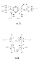
FIG. 3A is a diagram of a dual port NDRO cell, which can be utilized for the multiplexer of FIG. 2.
FIG. 3B is a block diagram of the circuit of FIG. 3A.
FIG. 4 is a diagram of a digital Mixer utilizing an NDRO cell to perform AND functionality asynchronously.
FIG. 5 is a circuit diagram of a resettable T flip-flop used in connection with the circuits of FIGS. 1, 2 and 4.
FIG. 6A is a diagram of a Reset-Set (RS) type NDRO cell used in the circuit of FIG. 1.
FIG. 6B is a partial Moore diagram of an RS-type NDRO cell used in FIG. 6A.
FIG. 7A is a circuit diagram of an XOR-type streaming mixer.
FIG. 7B is a diagram of a NDRO Multiplexer/Demultiplexer cell used in the XOR-type streaming mixer of FIG. 7A.
FIG. 8A is a circuit diagram of a D flip-flop used in the circuits of FIGS. 1, 2 and 4.
FIG. 8B is a partial Moore diagram of the circuit shown in FIG. 8A.
FIG. 9 is an exemplary layout of a digital I/Q Mixer illustrated in FIG. 1.
FIG. 10 is an exemplary layout of a digital I/Q Mixer utilized in FIG. 2.
FIG. 11 is an exemplary layout of a digital I/Q Mixer shown in FIG. 4.
FIG. 12 is a block diagram of a correlation receiver in accordance with one aspect of the invention.
FIG. 13 shows portions of the circuit of FIG. 12 in more detail.
DETAILED DESCRIPTION OF THE INVENTION
An important component of any digital receiver is a digital I/Q Mixer for converting narrowband (about 5 MHz) signals down from a few GHz. To achieve this goal with maximum efficiency the invention uses a circuit that is similar in principle to the Gilbert quadrature mixer. See article by B. Gilbert, “A Precise Four Quadrant Multiplier With Sub nanosecond Response,” IEEE. J. Solid-State Circuits, Vol. SC-3, pp. 365-373, December 1968. The basic idea of this mixer is to use square waves as a local oscillator signal instead of sine waves. The mathematical representation of a square wave is G(t)=sign[sin(ωLO·t)], where ωLO·t is a local oscillator frequency. The digital version of such a mixer is comparably easy to implement in RSFQ in case of single-bit coding, such as at the output of a delta-sigma modulator.
The first implementation of a square wave digital mixer in RSFQ is shown in FIG. 1. The right side of the device on the block diagram serves as a single-bit square wave generator with quadrature outputs. Although, FIG. 1 is shown as a two channel I/Q Mixer, the principles of the invention apply to a single channel mixer as well. As shown, the binary tree of resettable T flip-flops creates two (I and Q) local oscillator signals with 90 degree relative phase shift. The T flip-flops control RS-type NDRO cells, which, in turn, create digital square waves turning on and off a stream of SFQ pulses. A modulated signal gets mixed with 90 degree. shifted square waves in XOR cells, producing I channel and Q channel output products. An RS-type NDRO cell and a T flip-flop is used, instead of a T-type NDRO cell, in order to avoid a possible collision between the NDRO read-out pulse and reference pulse. Such a collision may cause a wrong phase shift between I and Q local oscillator signals. If such a problem occurs, the only way to correct it is by applying a RESET signal, and one would not want to do that too often. Despite its simple design, this version of the mixer has issues with timing, limiting its performance.
To avoid this problem, we have designed a second novel mixer performing single-bit-stream XOR multiplication (FIG. 2). In this case, we use the simple fact that A XOR 0=A and A XOR 1=Ā. A Rapid Single-Flux-Quantum (RSFQ) D flip-flop with complementary outputs (DFFC) (schematics and optimal parameters are in Kirichenko et al., “A 4-bit Single Flux Quantum Decoder,” IEEE Transactions on Applied Superconductivity, Vol. 5, No. 2, p. 2857, June 1995), converts the modulated signal into a single-bit data stream along with its inverted (complementary) representation. Multiplexing direct and inverted data outputs to the proper channel, it performs digital Quadrature signal down-conversion. After the modulated signal passes through a D flip-flop with complementary outputs (DFFC), it becomes asynchronous. Multiplexing direct and inverted data outputs to the proper channel, we effectively perform digital I/Q signal down-conversion. The multiplexing is done by two multiplexer cells controlled by the same T flip-flop binary tree as in FIG. 1, providing a 90 degree phase shift between I and Q channels. Again this circuit can be applied to single channel mixing as well as to I/Q quadrature mixing.
The multiplexer cell is shown in FIG. 3. This cell basically comprises a dual-port NDRO cell. From this cell, a designer can build either a demultiplexer by merging inputs A and B, or a multiplexer by merging outputs A and B. See article by Kirichenko et al., “A 4-bit Single Flux Quantum decoder,” IEEE Transactions on Applied Superconductivity, Vol. 5, No. 2, p. 2857, June 1995.
We have designed and fabricated the FIG. 3 version of the digital I/Q Mixer using the standard HYPRES 1 kA/cm2 fabrication process. The same design was also converted to the standard HYPRES 4.5 kA/cm2 fabrication process.
The multiplexing is done by two 2×1 RSFQ switches. The basic switch cell shown in FIG. 3A comprises a dual-port RSFQ Non-Destructive Read-Out (NDRO) cell with merged outputs, i.e., electrically connected outputs 1, 2. Applying an SFQ pulse to the input “Set A” causes the switch to connect input terminal “In A” to the output terminal “Out A” and disconnect terminal “In B”. Applying an SFQ pulse to the input “Set B” causes the switch to connect input terminal “In B” to the output terminal “Out B” and disconnect terminal “In A”. The optimized parameters for the cell in FIG. 3A are in Table 1.
TABLE 1
Optimized parameters for the dual-port
NDRO cell, normalized to reference
Critical 0.125 2.54 Bias 0.125
Current mA Inductance pH current mA
J1 2.94 L1 1.56 I1 1.92
J2 2.78 LQ1 0.60
J3 2.16 LQ2 1.22
J4 1.95 LJ1 0.03
J5 1.25 LJ4 0.04
J6 1.60 LJ5 0.06
J7 1.88 LJ6 0.29
J8 1.55 LJ7 0.50
J9 2.07 LJ8 0.01
J10 2.89 LJ9 0.51
LJ10 0.34
Both switches are controlled by a resettable T flip-flip binary tree. See description of T1 cell in S. Polonsky, et al., “Single Flux Quantum T flip-flop and its possible applications”, IEEE trans. On Appl. Supercond., vol. 4, p. 9, 1994, for the schematics and optimal parameters of the resettable TFF. The TFF tree converts a periodic reference signal into a control sequence of the switches, effectively creating two 90-degree phase-shifted Local Oscillator square-wave signals of a half reference signal frequency.
FIG. 4 is a diagram of a digital I/Q Mixer utilizing an NDRO cell to perform an AND function asynchronously. Like the other mixer designs, a reference clock drives a binary tree of T flip-flops with the outputs of the T flip-flop driving respective NDRO cells which perform an AND function with the data arriving from the delta-sigma modulator over a type D flip-flop.
Each of the three mixers described heretofore have their advantages and drawbacks. The circuit shown in FIG. 4, employing an AND operation has a poor signal-to-noise ratio because of a DC component in the local oscillator. However, it is feasible for a multi-bit implementation.
The digital I/Q Mixer employing XOR operation shown in FIG. 1, has good gain and a good signal-to-noise ratio but there is no obvious multi-bit implementation.
The streaming I/Q Mixer shown in FIG. 2, takes care of timing and synchronization issues, but may be hard to design for multi-bit data streams. Thus, each of the three mixers described is preferred for a particular application.
The XOR mixer shown in FIG. 1, utilizes a T flip-flop, an RS-type NDRO, an XOR cell and a D flip-flop (single output).
The streaming I/Q Mixer shown in FIG. 2 utilizes the multiplexer shown in FIG. 3 and a D flip-flop with complementary outputs.
The AND gate mixer shown in FIG. 4, utilizes T flip-flops, a multiplexer, such as that shown in FIG. 3, and a D flip-flop with complementary outputs. Each of these elements utilized to construct the mixers described so far will now be described in more detail.
FIG. 5 shows a circuit for construction of an SFQ resettable toggle flip-flop as used in the construction of the circuit of FIG. 1. The parameters for this schematic are found in the Polonsky article, S. Polonsky et al., “Single Flux, Quantum B Flip-flop and Its Possible Applications”, IEEE, vol. 4, no. 1, March 1994, p. 9.
The normalized “Personal Superconducting Circuit ANalayzer” (Polonsky, S.; Shevchenko, P.; Kirichenko, A.; Zinoviev, D.; Rylyakoy, A., “PSCAN'96: New Software for Simulation and Optimization of Complex RSFQ Circuits”, IEEE Transactions on Applied Superconductivity, Volume 7, Issue 2, June 1997 Page(s): 2685-2689) (PSCAN) units are normalized to 125 pA for junction critical currents in and bias current values I, and to 2.63 pA for inductance values L.
FIG. 6A is a diagram of an RS-type NDRO cell used in FIG. 1.
This cell functions as a Non-Destructive Read-Out with a single bit memory. One can change the state of the NDRO by applying the Reset or Set inputs. If the cell is in state “1”, then the Read input pulse goes to the Output. If the cell is in state “0”, then the Read input pulse is prevented from going to the Output.
The normalized PSCAN values for the circuit of FIG. 6A are as follows:
J1=3.15, J2=2.19, J3=2.21, J4=2.63, J5=1.32, J6=2.34, J7=2.39, J8=2.54, J9=2.02, J10=2.13,
I1=1.80, I2=2.42, I3=1.93,
LQ1=0.16, LQ2=0.16,
L1=1.37, L2=0.48, L3=0.10, L4=0.80, L5=0.53, L6=1.68, L7=0.66, L8=0.61, L9=0.32,
LJ2=0.80, LJ3=0.49, LJ4=0.21, LJ5=0.16, LJ6=0.25, LJ7=0.19,
XN=1.00.
FIG. 7A is a circuit diagram of an XOR-type streaming mixer, indicated by the MUX cell in FIG. 2.
FIG. 7B is a diagram of a Multiplexer/Demultiplexer cell used in the XOR circuit of FIG. 7A.
This RSFQ logic circuit functions as a multiplexer or demultiplexer, combining two input pulse streams into a single output stream or conversely. This was described in the U.S. Pat. No. 5,982,219, invented by A. Kirichenko (1999).
The normalized PSCAN values for the circuit of FIG. 7B are as follows: L1=4.51, L2=1.77, L3=0.37, L4=0.60, L5=0.30, L6=0.62, LC1=1.14, LC2=0.75.
FIG. 8A shows a circuit for an SFQ D flip-flop as used in the construction of the circuit of FIGS. 1 and 4 in which the complementary output is not used, and in FIG. 2, which uses the complementary output. If the data input is “1” (i.e., an SFQ pulse) then the True output gives “1” and the Complement gives “0”. If the data input is “0” (i.e., no SFQ pulse), then the True output gives “0” and the Complement gives “1”.
The normalized PSCAN values for the circuit of FIG. 8A are as follows:
I1=2.04, I2=4.45, I3=0.83,
J2=1.41, J3=1.41, J4=1.96, J5=2.42, J6=2.94, J7=2.82, J8=2.43, J9=1.96, J10=1.00,
L1=1.50, L2=0.30, L3=0.31, L4=0.74, L5=0.70, L6=2.28, L7=1.20, L8=1.20, L9=0.94, L10=2.00, L13=1.00,
LJ2=0.08, LJ3=0.29, LJ4=0.19, LJ5=0.09, LJ7=0.45,
LQ=0.23, LQ2=0.02.
FIG. 8B shows a partial Moore diagram of the D flip-flop used in FIG. 1.
FIG. 9 is an exemplary layout of a digital I/Q Mixer of the type shown in FIG. 1.
FIG. 10 is an exemplary layout of a digital I/Q Mixer of the type shown in FIG. 2.
FIG. 11 is an exemplary layout of a digital I/Q Mixer of the type shown in FIG. 4.
FIG. 12 is a block diagram of a correlation receiver in accordance with one aspect of the invention.
Turning to FIG. 13, Raw analog RF input is applied to an analog to digital convener (ADC) preferably to an oversampled delta modulator or delta sigma modulator. The output of the ADC is passed to a D flip-flop with complementary outputs and then to a multiplexer MUX. The output of the multiplexer is then passed to a chain of T flip-flops TFF1-TFF13 in this example the output (Digital Output) is taken from the last T flip-flop. The Digital Output is passed to another D flip-flop with complementary outputs to control the phase shift imported to a frequency reference by a string of alternating inverters and T flip-flop (TFF 1-4) cells. The output of the last T flip-flop connects to the set/reset inputs of the multiplexer of the streaming mixer.
While various embodiments of the present invention have been illustrated herein in detail, it should be apparent that modifications and adaptations to those embodiments may occur to those skilled in the art without departing from the scope of the present invention as set forth in the following claims.

Claims (20)

1. A digital mixer comprising:
an input circuit adapted to receive an incoming signal;
a reference circuit, adapted to receive a reference signal not synchronized with said incoming signal; and
a mixing circuit adapted to mix said incoming signal and said reference signal to generate an output signal having a spectrum with mixed signal products, comprising at least one superconducting non-destructive readout cell which does not receive a clock signal;
wherein at least one of the incoming signal and the reference signal is a multibit amplitude representation digital signal, generated by a circuit comprising a plurality of elements which are configured to generate concurrent digital data signals each having respectively a different magnitude relationship to the represented multibit amplitude.
2. The digital mixer of claim 1, wherein said mixing circuit comprises a Rapid Single Flux Quantum circuit.
3. The digital mixer of claim 2, wherein said mixing circuit further comprises an XOR gate.
4. The digital mixer of claim 1, wherein said mixing circuit comprises a pair of multiplexers.
5. The digital mixer of claim 1, wherein at least one of said input and reference circuit comprises a D flip-flop.
6. The digital mixer of claim 1, wherein at least one of said input and reference circuit comprises a T flip-flop.
7. A cross correlator using the digital mixer of claim 1.
8. A digital receiver using the cross correlator of claim 7.
9. A mixer for mixing a square wave reference signal with an incoming signal comprising:
a reference circuit adapted to receive said reference signal and adapted to produce a plurality of local signals with respectively different phases;
an input circuit adapted to receive said incoming signal and adapted to produce a plurality of input signals having respectively different phases;
wherein at least one of said plurality of local signals and said plurality of input signals is a multibit amplitude digital signal, generated by a circuit comprising a plurality of elements which are configured to generate concurrent digital data signals each having respectively a different magnitude relationship to the represented multibit amplitude;
a plurality of substantially unclocked mixing circuits, each adapted to receive a complementary set of said plurality of local signals and a complementary set of said plurality of input signals, each comprising a superconducting dual-port non-destructive readout cell; and
an output from each mixing circuit adapted to provide an output signal having a spectrum with mixed signal products of the incoming signal and a respective phase of the reference signal.
10. The mixer of claim 9, wherein said plurality of mixing circuits comprise Rapid Single Flux Quantum circuits.
11. The mixer of claim 10, wherein said plurality of mixing circuits further comprise an XOR gate.
12. The mixer of claim 9, in which said plurality of mixing circuits each comprise a multiplexer.
13. The mixer of claim 9, in which at least one of said reference circuit and said input circuit comprises a D flip-flop.
14. The mixer of claim 9, in which at least one of said reference circuit and said input circuit comprises a T flip-flop.
15. A digital mixing method, comprising:
receiving an incoming signal;
receiving a reference signal not synchronized with said incoming signal; and
mixing said incoming signal and said reference signal in a mixing circuit comprising at least one superconducting non-destructive readout cell which does not receive a clock signal, to generate an output signal having a spectrum with mixed signal products;
wherein at least one of the incoming signal and the reference signal is a concurrent multibit amplitude representation digital signal, each bit of the multibit amplitude representation having respectively a different magnitude relationship to the represented multibit amplitude.
16. The method of claim 15, wherein said mixing circuit comprises a Rapid Single Flux Quantum circuit.
17. The method of claim 16, wherein said mixing circuit comprises an XOR gate.
18. The method of claim 15, wherein said mixing circuit comprises a pair of multiplexers.
19. The method of claim 15, wherein at least one of said input signal and reference signal is received from a circuit comprising a D flip-flop.
20. The method of claim 15, wherein at least one of said input signal and reference signal is received from a circuit comprising a T flip-flop.
US12/725,426 2005-10-04 2010-03-16 Superconducting digital mixer Active US8050648B1 (en)

Priority Applications (1)

Application Number Priority Date Filing Date Title
US12/725,426 US8050648B1 (en) 2005-10-04 2010-03-16 Superconducting digital mixer

Applications Claiming Priority (2)

Application Number Priority Date Filing Date Title
US11/243,019 US7680474B2 (en) 2005-10-04 2005-10-04 Superconducting digital mixer
US12/725,426 US8050648B1 (en) 2005-10-04 2010-03-16 Superconducting digital mixer

Related Parent Applications (1)

Application Number Title Priority Date Filing Date
US11/243,019 Continuation US7680474B2 (en) 2005-10-04 2005-10-04 Superconducting digital mixer

Publications (1)

Publication Number Publication Date
US8050648B1 true US8050648B1 (en) 2011-11-01

Family

ID=37902529

Family Applications (2)

Application Number Title Priority Date Filing Date
US11/243,019 Active 2027-11-14 US7680474B2 (en) 2005-10-04 2005-10-04 Superconducting digital mixer
US12/725,426 Active US8050648B1 (en) 2005-10-04 2010-03-16 Superconducting digital mixer

Family Applications Before (1)

Application Number Title Priority Date Filing Date
US11/243,019 Active 2027-11-14 US7680474B2 (en) 2005-10-04 2005-10-04 Superconducting digital mixer

Country Status (1)

Country Link
US (2) US7680474B2 (en)

Cited By (4)

* Cited by examiner, † Cited by third party
Publication number Priority date Publication date Assignee Title
US9473124B1 (en) 2009-10-12 2016-10-18 Hypres, Inc. Low-power biasing networks for superconducting integrated circuits
US9906191B1 (en) 2010-08-02 2018-02-27 Hypres, Inc. Superconducting multi-bit digital mixer
US10222416B1 (en) 2015-04-14 2019-03-05 Hypres, Inc. System and method for array diagnostics in superconducting integrated circuit
US20220190830A1 (en) * 2020-12-10 2022-06-16 International Business Machines Corporation Rapid single flux quantum pulse multiplier

Families Citing this family (22)

* Cited by examiner, † Cited by third party
Publication number Priority date Publication date Assignee Title
US8462889B2 (en) 2005-10-04 2013-06-11 Hypres, Inc. Oversampling digital receiver for radio-frequency signals
US7616063B1 (en) * 2007-03-29 2009-11-10 Scientific Components Corporation Frequency synthesizer using a phase-locked loop and single side band mixer
US8344818B1 (en) * 2007-06-15 2013-01-01 Scientific Components Corporation Single side band (SSB) mixer
US8260144B2 (en) * 2008-03-12 2012-09-04 Hypres Inc. Digital radio frequency tranceiver system and method
US20120268190A1 (en) * 2011-04-19 2012-10-25 Icera Inc. Local oscillator clock signals
CN102413389B (en) * 2011-12-06 2014-07-02 烽火通信科技股份有限公司 Method for realizing intersection of asynchronous ODU0 (Optical Data Unit 0) with 80G volume
US8923439B1 (en) 2013-06-07 2014-12-30 Intel IP Corporation Complementary signal mixing
FR3021162B1 (en) * 2014-05-13 2017-10-06 Thales Sa MIXER CIRCUIT WITH COMPENSABLE HARMONIC CONTENT
US10650319B2 (en) 2015-02-06 2020-05-12 Northrop Grumman Systems Corporation Flux control of qubit under resonant excitation
US9543959B1 (en) * 2015-10-21 2017-01-10 Microsoft Technology Licensing, Llc Phase-mode based superconducting logic
US9673847B1 (en) * 2015-11-25 2017-06-06 Analog Devices, Inc. Apparatus and methods for transceiver calibration
US9979408B2 (en) 2016-05-05 2018-05-22 Analog Devices, Inc. Apparatus and methods for phase synchronization of phase-locked loops
US10411713B2 (en) 2017-02-04 2019-09-10 Microsoft Technology Licensing, Llc Superconducting circuits based devices and methods
US10756712B2 (en) 2017-11-13 2020-08-25 Northrop Grumman Systems Corporation RQL phase-mode flip-flop
US11082051B2 (en) 2018-05-11 2021-08-03 Analog Devices Global Unlimited Company Apparatus and methods for timing offset compensation in frequency synthesizers
US10615783B2 (en) 2018-07-31 2020-04-07 Northrop Grumman Systems Corporation RQL D flip-flops
US10554207B1 (en) * 2018-07-31 2020-02-04 Northrop Grumman Systems Corporation Superconducting non-destructive readout circuits
US11201608B2 (en) 2020-04-24 2021-12-14 Northrop Grumman Systems Corporation Superconducting latch system
CN111865461B (en) * 2020-05-25 2022-09-23 北京无线电测量研究所 Broadband multichannel digital TR circuit
US20230225225A1 (en) * 2020-06-01 2023-07-13 The Regents Of The University Of California System and method for superconducting silicon interconnect substrate with superconducting quantum processor
CN112394905B (en) * 2020-11-27 2022-11-08 重庆邮电大学 Design method of quantum divider
US20220344563A1 (en) * 2021-04-27 2022-10-27 Microsoft Technology Licensing, Llc Interfacing with superconducting circuitry

Citations (14)

* Cited by examiner, † Cited by third party
Publication number Priority date Publication date Assignee Title
US5406216A (en) * 1993-11-29 1995-04-11 Motorola, Inc. Technique and method for asynchronous scan design
US5631929A (en) * 1995-05-09 1997-05-20 Unisys Corporation Electronic transmitter having a digital combiner circuit for transmitting multiple digital input signals simultaneously
US5818373A (en) 1996-12-19 1998-10-06 Research Foundation Of State University Of New York Interface between superconductor and semiconductor electronic circuits using phase-shift keying coded output data format
US5963351A (en) * 1996-08-23 1999-10-05 Conductus, Inc. Digital optical receiver with instantaneous Josephson clock recovery circuit
US6420895B1 (en) * 2001-03-23 2002-07-16 Trw Inc. High-sensitivity, self-clocked receiver for multi-chip superconductor circuits
US20040022332A1 (en) * 2002-08-02 2004-02-05 Deepnarayan Gupta Digital RF correlator for multipurpose digital signal processing
US6724216B2 (en) 2001-05-14 2004-04-20 Fujitsu Limited Rapid single-flux-quantum logic circuit and rapid single-flux-quantum output conversion circuit
US20040120299A1 (en) 2002-12-18 2004-06-24 Anna Kidiyarova-Shevchenko Method and apparatus for multi-user detection using RFSQ successive interference cancellation in CDMA wireless systems
US6836154B2 (en) 2000-08-30 2004-12-28 Telefonaktiebolaget Lm Ericsson (Publ) Direction sensitive and phase-inversion free phase detectors
US6917537B2 (en) 2003-08-11 2005-07-12 Northrop Grumman Corporation RSFQ Batcher-banyan switching network
US20050235027A1 (en) 2004-04-14 2005-10-20 Jung Ku R Arithmetic and logic unit using half adder
US20070021933A1 (en) * 2003-08-29 2007-01-25 Koninklijke Philips Electronics N.V. Phase detector
US7257609B1 (en) * 2000-10-16 2007-08-14 Nokia Corporation Multiplier and shift device using signed digit representation
US7944253B1 (en) * 2005-10-04 2011-05-17 Hypres, Inc. Digital programmable frequency divider

Family Cites Families (2)

* Cited by examiner, † Cited by third party
Publication number Priority date Publication date Assignee Title
US5140324A (en) * 1991-06-06 1992-08-18 Westinghouse Electric Corp. Superconducting sigma-delta analog-to-digital converter
US5289400A (en) * 1992-07-30 1994-02-22 Westinghouse Electric Corp. Single-flux-quantum multiply-accumulator

Patent Citations (14)

* Cited by examiner, † Cited by third party
Publication number Priority date Publication date Assignee Title
US5406216A (en) * 1993-11-29 1995-04-11 Motorola, Inc. Technique and method for asynchronous scan design
US5631929A (en) * 1995-05-09 1997-05-20 Unisys Corporation Electronic transmitter having a digital combiner circuit for transmitting multiple digital input signals simultaneously
US5963351A (en) * 1996-08-23 1999-10-05 Conductus, Inc. Digital optical receiver with instantaneous Josephson clock recovery circuit
US5818373A (en) 1996-12-19 1998-10-06 Research Foundation Of State University Of New York Interface between superconductor and semiconductor electronic circuits using phase-shift keying coded output data format
US6836154B2 (en) 2000-08-30 2004-12-28 Telefonaktiebolaget Lm Ericsson (Publ) Direction sensitive and phase-inversion free phase detectors
US7257609B1 (en) * 2000-10-16 2007-08-14 Nokia Corporation Multiplier and shift device using signed digit representation
US6420895B1 (en) * 2001-03-23 2002-07-16 Trw Inc. High-sensitivity, self-clocked receiver for multi-chip superconductor circuits
US6724216B2 (en) 2001-05-14 2004-04-20 Fujitsu Limited Rapid single-flux-quantum logic circuit and rapid single-flux-quantum output conversion circuit
US20040022332A1 (en) * 2002-08-02 2004-02-05 Deepnarayan Gupta Digital RF correlator for multipurpose digital signal processing
US20040120299A1 (en) 2002-12-18 2004-06-24 Anna Kidiyarova-Shevchenko Method and apparatus for multi-user detection using RFSQ successive interference cancellation in CDMA wireless systems
US6917537B2 (en) 2003-08-11 2005-07-12 Northrop Grumman Corporation RSFQ Batcher-banyan switching network
US20070021933A1 (en) * 2003-08-29 2007-01-25 Koninklijke Philips Electronics N.V. Phase detector
US20050235027A1 (en) 2004-04-14 2005-10-20 Jung Ku R Arithmetic and logic unit using half adder
US7944253B1 (en) * 2005-10-04 2011-05-17 Hypres, Inc. Digital programmable frequency divider

Non-Patent Citations (7)

* Cited by examiner, † Cited by third party
Title
Fei, "Frequency Divider Design Strategies", Broadband Technology, Mar. 2005, pp. 18-26.
Gilbert, "A Precise Four-Quadrant Multiplier with Subnanosecond Response", IEEE, vol. SC-3, Dec. 1968, pp, 365-373.
Kirichenko, et al., "4-bit Rapid Single-Flux-Quantum Decoder", IEEE, vol. 5, No. 2, Mar. 1995, pp. 2857-2860.
Kirichenko, et al., "Superconductor Digital Receiver Components", IEEE, vol. 15, No. 2, Jun. 2005, pp. 1-7.
Likharev, et al, "RSFQ Logic/Memory Family: A New Josephson-Junction Technology for Sub-Terahertz-Clock-Frequency Digital Systems", IEEE Transactions on Applied Superconductivity, vol. 1, No. 1, Mar. 1991, pp. 3-28.
Polonsky, et al., "Single Flux, Quantum B Flip-Flop and Its Possible Applications", IEEE, vol. 4, No. 1, Mar. 1994, pp. 9-18.
Yu, et al., "RSFQ Asynchronous Serial Multiplier and Spreading Codes Generator for Multiuser Detector", IEEE, vol. 13, No. 2, Jun. 2003, pp. 429-432.

Cited By (6)

* Cited by examiner, † Cited by third party
Publication number Priority date Publication date Assignee Title
US9473124B1 (en) 2009-10-12 2016-10-18 Hypres, Inc. Low-power biasing networks for superconducting integrated circuits
US9853645B1 (en) 2009-10-12 2017-12-26 Hypres, Inc. Low-power biasing networks for superconducting integrated circuits
US9906191B1 (en) 2010-08-02 2018-02-27 Hypres, Inc. Superconducting multi-bit digital mixer
US10222416B1 (en) 2015-04-14 2019-03-05 Hypres, Inc. System and method for array diagnostics in superconducting integrated circuit
US20220190830A1 (en) * 2020-12-10 2022-06-16 International Business Machines Corporation Rapid single flux quantum pulse multiplier
US11411564B2 (en) * 2020-12-10 2022-08-09 International Business Machines Corporation Rapid single flux quantum pulse multiplier

Also Published As

Publication number Publication date
US20070077906A1 (en) 2007-04-05
US7680474B2 (en) 2010-03-16

Similar Documents

Publication Publication Date Title
US8050648B1 (en) Superconducting digital mixer
US7554369B2 (en) Digital programmable frequency divider
Soloviev et al. Beyond Moore’s technologies: operation principles of a superconductor alternative
Mukhanov et al. Superconductor analog-to-digital converters
US6614371B2 (en) Synchronous data serialization circuit
US20170201224A1 (en) Superconducting logic compatible phase shifter
US20070293160A1 (en) Digital Routing Switch Matrix for Digitized Radio-Frequency Signals
US10411713B2 (en) Superconducting circuits based devices and methods
JPH11154867A (en) Correlative superconducting conductor single magnetic flux quantum analog digital conveter
Wikborg et al. RSFQ front-end for a software radio receiver
JP2007329797A (en) Superconducting single flux quantum modulation circuit
US7750664B2 (en) Digital programmable phase generator
US5818373A (en) Interface between superconductor and semiconductor electronic circuits using phase-shift keying coded output data format
Kirichenko et al. 4-bit rapid single-flux-quantum decoder
Likharev Superconductors speed up computation
US5982219A (en) Asynchronous dual-rail demultiplexer employing Josephson junctions
JP6952404B2 (en) Switching frequency-multiplexed microwave signals using cascading multipath interference Josephson switches with non-overlapping bandwidth
JPH1092188A (en) Ultra-high speed shift register utilizing resonance tunnel diode
US4678945A (en) Unidirectional single-flux-quantum logic circuit
Balashov et al. Passive phase shifter for superconducting Josephson circuits
Kirichenko High-speed asynchronous data multiplexing/demultiplexing
Cong et al. Superconductor Logic Implementation with All-JJ Inductor-Free Cell Library
Koch et al. A NRZ-output amplifier for RSFQ circuits
Mukhanov Superconductive single-flux quantum technology
Ke et al. Single flux quantum circuits using the residue number system

Legal Events

Date Code Title Description
STCF Information on status: patent grant

Free format text: PATENTED CASE

FPAY Fee payment

Year of fee payment: 4

AS Assignment

Owner name: SEEQC,INC., NEW YORK

Free format text: ASSIGNMENT OF ASSIGNORS INTEREST;ASSIGNOR:HYPRES, INC.;REEL/FRAME:049412/0196

Effective date: 20190421

FEPP Fee payment procedure

Free format text: MAINTENANCE FEE REMINDER MAILED (ORIGINAL EVENT CODE: REM.); ENTITY STATUS OF PATENT OWNER: SMALL ENTITY

FEPP Fee payment procedure

Free format text: 7.5 YR SURCHARGE - LATE PMT W/IN 6 MO, SMALL ENTITY (ORIGINAL EVENT CODE: M2555); ENTITY STATUS OF PATENT OWNER: SMALL ENTITY

MAFP Maintenance fee payment

Free format text: PAYMENT OF MAINTENANCE FEE, 8TH YR, SMALL ENTITY (ORIGINAL EVENT CODE: M2552); ENTITY STATUS OF PATENT OWNER: SMALL ENTITY

Year of fee payment: 8

FEPP Fee payment procedure

Free format text: MAINTENANCE FEE REMINDER MAILED (ORIGINAL EVENT CODE: REM.); ENTITY STATUS OF PATENT OWNER: SMALL ENTITY

FEPP Fee payment procedure

Free format text: 11.5 YR SURCHARGE- LATE PMT W/IN 6 MO, SMALL ENTITY (ORIGINAL EVENT CODE: M2556); ENTITY STATUS OF PATENT OWNER: SMALL ENTITY

MAFP Maintenance fee payment

Free format text: PAYMENT OF MAINTENANCE FEE, 12TH YR, SMALL ENTITY (ORIGINAL EVENT CODE: M2553); ENTITY STATUS OF PATENT OWNER: SMALL ENTITY

Year of fee payment: 12