US8063426B2 - Fast switching power insulated gate semiconductor device - Google Patents
Fast switching power insulated gate semiconductor device Download PDFInfo
- Publication number
- US8063426B2 US8063426B2 US12/021,037 US2103708A US8063426B2 US 8063426 B2 US8063426 B2 US 8063426B2 US 2103708 A US2103708 A US 2103708A US 8063426 B2 US8063426 B2 US 8063426B2
- Authority
- US
- United States
- Prior art keywords
- gate
- fiss
- iiss
- capacitance
- mosfet
- Prior art date
- Legal status (The legal status is an assumption and is not a legal conclusion. Google has not performed a legal analysis and makes no representation as to the accuracy of the status listed.)
- Expired - Fee Related, expires
Links
- 239000004065 semiconductor Substances 0.000 title abstract description 6
- 238000009413 insulation Methods 0.000 claims abstract description 14
- 239000003990 capacitor Substances 0.000 claims description 15
- 230000005669 field effect Effects 0.000 claims description 7
- XUIMIQQOPSSXEZ-UHFFFAOYSA-N Silicon Chemical compound [Si] XUIMIQQOPSSXEZ-UHFFFAOYSA-N 0.000 claims description 6
- 229910044991 metal oxide Inorganic materials 0.000 claims description 6
- 150000004706 metal oxides Chemical class 0.000 claims description 6
- 229910052710 silicon Inorganic materials 0.000 claims description 6
- 239000010703 silicon Substances 0.000 claims description 6
- 239000008186 active pharmaceutical agent Substances 0.000 description 8
- 230000003247 decreasing effect Effects 0.000 description 5
- 238000010586 diagram Methods 0.000 description 5
- 230000000694 effects Effects 0.000 description 5
- 238000000034 method Methods 0.000 description 5
- 230000006378 damage Effects 0.000 description 2
- 238000000151 deposition Methods 0.000 description 2
- 101150068246 V-MOS gene Proteins 0.000 description 1
- 230000000052 comparative effect Effects 0.000 description 1
- 230000014509 gene expression Effects 0.000 description 1
- 238000010606 normalization Methods 0.000 description 1
Images


Classifications
-
- H—ELECTRICITY
- H01—ELECTRIC ELEMENTS
- H01L—SEMICONDUCTOR DEVICES NOT COVERED BY CLASS H10
- H01L29/00—Semiconductor devices adapted for rectifying, amplifying, oscillating or switching, or capacitors or resistors with at least one potential-jump barrier or surface barrier, e.g. PN junction depletion layer or carrier concentration layer; Details of semiconductor bodies or of electrodes thereof ; Multistep manufacturing processes therefor
- H01L29/66—Types of semiconductor device ; Multistep manufacturing processes therefor
- H01L29/68—Types of semiconductor device ; Multistep manufacturing processes therefor controllable by only the electric current supplied, or only the electric potential applied, to an electrode which does not carry the current to be rectified, amplified or switched
- H01L29/76—Unipolar devices, e.g. field effect transistors
- H01L29/772—Field effect transistors
- H01L29/78—Field effect transistors with field effect produced by an insulated gate
- H01L29/7801—DMOS transistors, i.e. MISFETs with a channel accommodating body or base region adjoining a drain drift region
- H01L29/7802—Vertical DMOS transistors, i.e. VDMOS transistors
-
- H—ELECTRICITY
- H01—ELECTRIC ELEMENTS
- H01L—SEMICONDUCTOR DEVICES NOT COVERED BY CLASS H10
- H01L29/00—Semiconductor devices adapted for rectifying, amplifying, oscillating or switching, or capacitors or resistors with at least one potential-jump barrier or surface barrier, e.g. PN junction depletion layer or carrier concentration layer; Details of semiconductor bodies or of electrodes thereof ; Multistep manufacturing processes therefor
- H01L29/40—Electrodes ; Multistep manufacturing processes therefor
- H01L29/41—Electrodes ; Multistep manufacturing processes therefor characterised by their shape, relative sizes or dispositions
- H01L29/423—Electrodes ; Multistep manufacturing processes therefor characterised by their shape, relative sizes or dispositions not carrying the current to be rectified, amplified or switched
- H01L29/42312—Gate electrodes for field effect devices
- H01L29/42316—Gate electrodes for field effect devices for field-effect transistors
- H01L29/4232—Gate electrodes for field effect devices for field-effect transistors with insulated gate
- H01L29/42364—Gate electrodes for field effect devices for field-effect transistors with insulated gate characterised by the insulating layer, e.g. thickness or uniformity
-
- H—ELECTRICITY
- H03—ELECTRONIC CIRCUITRY
- H03K—PULSE TECHNIQUE
- H03K17/00—Electronic switching or gating, i.e. not by contact-making and –breaking
- H03K17/04—Modifications for accelerating switching
- H03K17/041—Modifications for accelerating switching without feedback from the output circuit to the control circuit
- H03K17/0412—Modifications for accelerating switching without feedback from the output circuit to the control circuit by measures taken in the control circuit
- H03K17/04123—Modifications for accelerating switching without feedback from the output circuit to the control circuit by measures taken in the control circuit in field-effect transistor switches
-
- H—ELECTRICITY
- H01—ELECTRIC ELEMENTS
- H01L—SEMICONDUCTOR DEVICES NOT COVERED BY CLASS H10
- H01L25/00—Assemblies consisting of a plurality of individual semiconductor or other solid state devices ; Multistep manufacturing processes thereof
- H01L25/03—Assemblies consisting of a plurality of individual semiconductor or other solid state devices ; Multistep manufacturing processes thereof all the devices being of a type provided for in the same subgroup of groups H01L27/00 - H01L33/00, or in a single subclass of H10K, H10N, e.g. assemblies of rectifier diodes
- H01L25/04—Assemblies consisting of a plurality of individual semiconductor or other solid state devices ; Multistep manufacturing processes thereof all the devices being of a type provided for in the same subgroup of groups H01L27/00 - H01L33/00, or in a single subclass of H10K, H10N, e.g. assemblies of rectifier diodes the devices not having separate containers
- H01L25/07—Assemblies consisting of a plurality of individual semiconductor or other solid state devices ; Multistep manufacturing processes thereof all the devices being of a type provided for in the same subgroup of groups H01L27/00 - H01L33/00, or in a single subclass of H10K, H10N, e.g. assemblies of rectifier diodes the devices not having separate containers the devices being of a type provided for in group H01L29/00
-
- H—ELECTRICITY
- H01—ELECTRIC ELEMENTS
- H01L—SEMICONDUCTOR DEVICES NOT COVERED BY CLASS H10
- H01L2924/00—Indexing scheme for arrangements or methods for connecting or disconnecting semiconductor or solid-state bodies as covered by H01L24/00
- H01L2924/0001—Technical content checked by a classifier
- H01L2924/0002—Not covered by any one of groups H01L24/00, H01L24/00 and H01L2224/00
Landscapes
- Microelectronics & Electronic Packaging (AREA)
- Engineering & Computer Science (AREA)
- Power Engineering (AREA)
- Condensed Matter Physics & Semiconductors (AREA)
- General Physics & Mathematics (AREA)
- Physics & Mathematics (AREA)
- Ceramic Engineering (AREA)
- Computer Hardware Design (AREA)
- Semiconductor Integrated Circuits (AREA)
- Electronic Switches (AREA)
- Insulated Gate Type Field-Effect Transistor (AREA)
- Metal-Oxide And Bipolar Metal-Oxide Semiconductor Integrated Circuits (AREA)
- Closed-Circuit Television Systems (AREA)
Abstract
Description
β≡A(1/C iiss−1/C fiss)=∝max.
d≧d min≈β/[(Q G(max) /Q G(min))−1]
where QG(max) is the maximum allowable steady state charge for safe operation and QG(min) is the minimum charge required for complete switching.
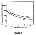
where A is an effective area, which includes proper normalization constants. Thus, ∝ is a maximum (∝max) when the device is switched off as shown in
β≡A(1/C iiss−1/C fiss)=∝max.
d ins≧β/[(Q G(max) /Q G(min))−1]
wherein QG(min) is the minimum charge required for complete switching and wherein QG(max) is the maximum allowable gate charge on the device which includes a safety margin. Destruction will occur when Q≧QG(max).
d ins≧β/[(V GS(max)/VGS(min))−1]
∈s =L s di/dt+iR s
∈s(max) ≈L s I DS(max) /T s +I DS(max) R s.
| TABLE 1 | ||||||
| No. | Modified Input Gate Capacitance Ciiss, Cfiss (nF) |
|
Applied Gate Voltage VGS (volt) | Initial & Final Gate Charge Transferred CiissVGS & CfissVGS (nC) | Turn-on Delay Time Predicted & Observed Td(on) (ns) | Measured Switching Time Ts (ns) |
| i | 1.2 2.6 | 2.16 | 15 | 18 40 | 6.3 6 | 38 |
| (20 ns/div) | ||||||
| ii | 0.86 1.4 | 1.63 | 32 | 28 45 | 5.3 5 | 20 |
| (20 ns/div) | ||||||
| iii | 0.58 0.78 | 1.34 | 120 | 70 94 | 4.4 <2 | <4 |
| (10 ns/div) | ||||||
| iv | 0.35 0.41 | 1.17 | 200 | 70 82 | 3.4 <2 | <4 |
| (10 ns/div) | ||||||
∈s(max)≈7.4 nH(40 A/27 ns)+4 volt=15 volt
V G(internal) ≈V GS(max)−∈s(max)=20 volt−15 volt=5 volt
∈s(max)≈7.4 nH(40 A/2.5 ns)+5 volt=123 volt
V G(internal) ≈V GS(max)−∈s(max)≈200 volt−123 volt=77 volt
T don≈(2π/3)(L S C iiss)1/2.
Ts∝1/dins 1/2
which indicates that the total switching time is reduced by increasing the effective thickness dins of
Q G =V GS C iiss ≧Q G(min).
V GS ≧V GS(min)=Q G(min) /C iiss.
Also,
Q G =V GS C fiss ≦Q G(max)
and the corresponding voltage limit is given by
V GS ≦V GS(max) =Q G(max) /C fiss.
C fiss /C iiss ≦Q G(max) /Q G(min)
or
C fiss /C iiss ≦V GS(max) /V GS(min).
(2π/3)2 Q G(min) L S ≦V ES T S≦(2π/3)2 Q G(max) L S
which means that the operating voltage VGS of the device according to the invention (which is much higher than the corresponding voltage for prior art devices) is limited as follows:
(2π/3)2 Q G(min) L S /T S 2 ≦V GS≦(2π/3)2 Q G(max) L S /T S 2
and as illustrated in
Claims (18)
Priority Applications (1)
| Application Number | Priority Date | Filing Date | Title |
|---|---|---|---|
| US12/021,037 US8063426B2 (en) | 2003-01-21 | 2008-01-28 | Fast switching power insulated gate semiconductor device |
Applications Claiming Priority (5)
| Application Number | Priority Date | Filing Date | Title |
|---|---|---|---|
| ZA2003/0552 | 2003-01-21 | ||
| ZA200300552 | 2003-01-21 | ||
| PCT/ZA2004/000005 WO2004066395A2 (en) | 2003-01-21 | 2004-01-21 | Fast switching power insulated gate semiconductor device |
| US10/542,720 US20060118832A1 (en) | 2003-01-21 | 2004-01-21 | Fast switching power insulated gate semiconductor device |
| US12/021,037 US8063426B2 (en) | 2003-01-21 | 2008-01-28 | Fast switching power insulated gate semiconductor device |
Related Parent Applications (3)
| Application Number | Title | Priority Date | Filing Date |
|---|---|---|---|
| PCT/ZA2004/000005 Continuation WO2004066395A2 (en) | 2003-01-21 | 2004-01-21 | Fast switching power insulated gate semiconductor device |
| US10/542,720 Continuation US20060118832A1 (en) | 2003-01-21 | 2004-01-21 | Fast switching power insulated gate semiconductor device |
| US11/542,720 Continuation US7835749B1 (en) | 2006-10-03 | 2006-10-03 | Location inspector in wireless networks |
Publications (2)
| Publication Number | Publication Date |
|---|---|
| US20080203457A1 US20080203457A1 (en) | 2008-08-28 |
| US8063426B2 true US8063426B2 (en) | 2011-11-22 |
Family
ID=32772476
Family Applications (2)
| Application Number | Title | Priority Date | Filing Date |
|---|---|---|---|
| US10/542,720 Abandoned US20060118832A1 (en) | 2003-01-21 | 2004-01-21 | Fast switching power insulated gate semiconductor device |
| US12/021,037 Expired - Fee Related US8063426B2 (en) | 2003-01-21 | 2008-01-28 | Fast switching power insulated gate semiconductor device |
Family Applications Before (1)
| Application Number | Title | Priority Date | Filing Date |
|---|---|---|---|
| US10/542,720 Abandoned US20060118832A1 (en) | 2003-01-21 | 2004-01-21 | Fast switching power insulated gate semiconductor device |
Country Status (8)
| Country | Link |
|---|---|
| US (2) | US20060118832A1 (en) |
| EP (1) | EP1586120B1 (en) |
| JP (2) | JP5362955B2 (en) |
| CN (1) | CN100508211C (en) |
| ES (1) | ES2578678T3 (en) |
| HK (1) | HK1091321A1 (en) |
| WO (1) | WO2004066395A2 (en) |
| ZA (1) | ZA200505759B (en) |
Families Citing this family (3)
| Publication number | Priority date | Publication date | Assignee | Title |
|---|---|---|---|---|
| US8039897B2 (en) * | 2008-12-19 | 2011-10-18 | Fairchild Semiconductor Corporation | Lateral MOSFET with substrate drain connection |
| US20120019284A1 (en) * | 2010-07-26 | 2012-01-26 | Infineon Technologies Austria Ag | Normally-Off Field Effect Transistor, a Manufacturing Method Therefor and a Method for Programming a Power Field Effect Transistor |
| CN104604133B (en) * | 2012-08-28 | 2017-03-01 | 夏普株式会社 | Compound semiconductor device |
Citations (39)
| Publication number | Priority date | Publication date | Assignee | Title |
|---|---|---|---|---|
| US3883413A (en) | 1972-09-25 | 1975-05-13 | Avco Corp | Ozone generator using pulsed electron beam and decaying electric field |
| US4038165A (en) | 1975-03-13 | 1977-07-26 | Union Carbide Corporation | Corona reaction method |
| US4438356A (en) | 1982-03-24 | 1984-03-20 | International Rectifier Corporation | Solid state relay circuit employing MOSFET power switching devices |
| US4471245A (en) | 1982-06-21 | 1984-09-11 | Eaton Corporation | FET Gating circuit with fast turn-on capacitor |
| US4491807A (en) | 1982-05-20 | 1985-01-01 | Rca Corporation | FET Negative resistance circuits |
| JPS6038877A (en) | 1983-08-12 | 1985-02-28 | Hitachi Ltd | Insulated gate semiconductor device |
| US4683387A (en) * | 1985-12-03 | 1987-07-28 | The United States Of America As Represented By The Secretary Of The Air Force | Quadrature switch apparatus for multi mode phase shift drivers |
| US4695936A (en) | 1986-02-07 | 1987-09-22 | Astec Components, Ltd. | Switching mode power supply start circuit |
| US4713220A (en) | 1985-04-22 | 1987-12-15 | National Distillers And Chemical Corporation | Ozonator power supply |
| US4736121A (en) | 1985-09-10 | 1988-04-05 | Sos Microelettronica S.p.A. | Charge pump circuit for driving N-channel MOS transistors |
| US4764857A (en) | 1987-05-06 | 1988-08-16 | Zenith Electronics Corporation | Power supply start-up circuit with high frequency transformer |
| US4796174A (en) | 1986-04-04 | 1989-01-03 | Sgs-Thomson Microelectronics S.A. | Direct voltage multiplier capable of being integrated into a semiconducting structure |
| GB2206731A (en) | 1987-06-08 | 1989-01-11 | Philips Electronic Associated | A semiconductor device and a circuit for an intelligent power switch |
| US4869881A (en) | 1988-05-03 | 1989-09-26 | Pillar Technologies, Inc. | Ozone generator system |
| US4873460A (en) | 1988-11-16 | 1989-10-10 | California Institute Of Technology | Monolithic transistor gate energy recovery system |
| US4912335A (en) | 1988-03-07 | 1990-03-27 | Dionics Inc. | Means for rapid charging and dynamic discharging of a capacitively charged electrical device |
| US5016070A (en) | 1989-06-30 | 1991-05-14 | Texas Instruments Incorporated | Stacked CMOS sRAM with vertical transistors and cross-coupled capacitors |
| WO1991011826A1 (en) | 1990-02-01 | 1991-08-08 | Quigg Fred L | Mosfet structure having reduced gate capacitance and method of forming same |
| US5140201A (en) | 1990-04-02 | 1992-08-18 | Mitsubishi Denki Kabushiki Kaisha | Gate drive circuit for insulated gate semiconductor device and flash controller using the circuit |
| US5392187A (en) | 1992-08-12 | 1995-02-21 | North Carolina State University At Raleigh | Integrated circuit power device with transient responsive current limiting means |
| US5475333A (en) | 1991-05-10 | 1995-12-12 | Fuji Electric Co., Ltd. | Built-in drive power-source semiconductor device |
| US5504449A (en) | 1992-04-09 | 1996-04-02 | Harris Corporation | Power driver circuit |
| JPH08321602A (en) | 1995-05-26 | 1996-12-03 | Fuji Electric Co Ltd | Mis semiconductor device and controlling method thereof |
| US5977588A (en) * | 1997-10-31 | 1999-11-02 | Stmicroelectronics, Inc. | Radio frequency power MOSFET device having improved performance characteristics |
| DE19905421A1 (en) | 1999-02-10 | 2000-08-24 | Semikron Elektronik Gmbh | Power semiconductor component with reduced Miller capacity such as IGBT or MOSFET in current rectifier, half-bridges, and switches |
| EP1096573A2 (en) | 1999-10-27 | 2001-05-02 | Intersil Corporation | Technique for minimizing gate charge and gate to drain capacitance in power MOS devices such as DMOS, IGBTs and MOSFETs |
| US6291298B1 (en) * | 1999-05-25 | 2001-09-18 | Advanced Analogic Technologies, Inc. | Process of manufacturing Trench gate semiconductor device having gate oxide layer with multiple thicknesses |
| WO2002013257A2 (en) | 2000-08-04 | 2002-02-14 | Infineon Technologies Ag | Semiconductor switch element comprising two control electrodes, which can be controlled by means of field effect |
| US6441652B1 (en) | 1999-06-24 | 2002-08-27 | Koninklijke Philips Electroanics N.V. | High efficiency high frequency resonant gate driver for power converter |
| US6566708B1 (en) | 2000-11-17 | 2003-05-20 | Koninklijke Philips Electronics N.V. | Trench-gate field-effect transistors with low gate-drain capacitance and their manufacture |
| US6573560B2 (en) | 2001-11-06 | 2003-06-03 | Fairchild Semiconductor Corporation | Trench MOSFET with reduced Miller capacitance |
| US6589830B1 (en) | 2000-09-20 | 2003-07-08 | Fairchild Semiconductor Corporation | Self-aligned process for fabricating power MOSFET with spacer-shaped terraced gate |
| US20030173619A1 (en) | 2002-03-15 | 2003-09-18 | Martin Feldtkeller | Circuit configuration and method for the switch-on/off control of a field-effect transistor |
| US6690062B2 (en) | 2002-03-19 | 2004-02-10 | Infineon Technologies Ag | Transistor configuration with a shielding electrode outside an active cell array and a reduced gate-drain capacitance |
| US6707102B2 (en) | 2000-09-19 | 2004-03-16 | Renesas Technology Corp. | Semiconductor device including an insulated gate type field effect transistor and method for fabricating the same |
| US6759835B2 (en) | 2001-12-21 | 2004-07-06 | Goodrich Control Systems, Ltd. | Switch control circuit |
| US20040251484A1 (en) | 1999-09-13 | 2004-12-16 | Masayuki Miyazaki | Semiconductor integrated circuit device |
| US6870220B2 (en) * | 2002-08-23 | 2005-03-22 | Fairchild Semiconductor Corporation | Method and apparatus for improved MOS gating to reduce miller capacitance and switching losses |
| US6870405B2 (en) | 1999-02-24 | 2005-03-22 | Potchefstroom University For Christian Higher Education | Method for driving an insulated gate semiconductor device using a short duration pulse |
Family Cites Families (5)
| Publication number | Priority date | Publication date | Assignee | Title |
|---|---|---|---|---|
| SE456291B (en) * | 1980-02-22 | 1988-09-19 | Rca Corp | VERTICAL MOSPHET DEVICE INCLUDING A COLLECTOR AREA LOCATED ON SCREEN ELECTRODE FOR MINIMIZER MILLER CAPACITANCE AND POWER DISTURBANCE |
| JP2975646B2 (en) * | 1989-06-30 | 1999-11-10 | テキサス インスツルメンツ インコーポレイテツド | Integrated device |
| JPH03138981A (en) * | 1989-10-25 | 1991-06-13 | Hitachi Ltd | Semiconductor element |
| JPH03228376A (en) * | 1990-02-02 | 1991-10-09 | Nippon Telegr & Teleph Corp <Ntt> | Vertical double diffused mosfet |
| JPH05335582A (en) * | 1992-05-27 | 1993-12-17 | Omron Corp | Vertical mosfet device and manufacture thereof |
-
2004
- 2004-01-21 JP JP2006501327A patent/JP5362955B2/en not_active Expired - Fee Related
- 2004-01-21 CN CNB2004800069694A patent/CN100508211C/en not_active Expired - Fee Related
- 2004-01-21 WO PCT/ZA2004/000005 patent/WO2004066395A2/en active Search and Examination
- 2004-01-21 EP EP04737345.1A patent/EP1586120B1/en not_active Expired - Lifetime
- 2004-01-21 US US10/542,720 patent/US20060118832A1/en not_active Abandoned
- 2004-01-21 ES ES04737345.1T patent/ES2578678T3/en not_active Expired - Lifetime
-
2005
- 2005-07-19 ZA ZA200505759A patent/ZA200505759B/en unknown
-
2006
- 2006-10-27 HK HK06111869.9A patent/HK1091321A1/en not_active IP Right Cessation
-
2008
- 2008-01-28 US US12/021,037 patent/US8063426B2/en not_active Expired - Fee Related
-
2013
- 2013-05-20 JP JP2013106189A patent/JP2013179344A/en active Pending
Patent Citations (41)
| Publication number | Priority date | Publication date | Assignee | Title |
|---|---|---|---|---|
| US3883413A (en) | 1972-09-25 | 1975-05-13 | Avco Corp | Ozone generator using pulsed electron beam and decaying electric field |
| US4038165A (en) | 1975-03-13 | 1977-07-26 | Union Carbide Corporation | Corona reaction method |
| US4438356A (en) | 1982-03-24 | 1984-03-20 | International Rectifier Corporation | Solid state relay circuit employing MOSFET power switching devices |
| US4491807A (en) | 1982-05-20 | 1985-01-01 | Rca Corporation | FET Negative resistance circuits |
| US4471245A (en) | 1982-06-21 | 1984-09-11 | Eaton Corporation | FET Gating circuit with fast turn-on capacitor |
| JPS6038877A (en) | 1983-08-12 | 1985-02-28 | Hitachi Ltd | Insulated gate semiconductor device |
| US4713220A (en) | 1985-04-22 | 1987-12-15 | National Distillers And Chemical Corporation | Ozonator power supply |
| US4736121A (en) | 1985-09-10 | 1988-04-05 | Sos Microelettronica S.p.A. | Charge pump circuit for driving N-channel MOS transistors |
| US4683387A (en) * | 1985-12-03 | 1987-07-28 | The United States Of America As Represented By The Secretary Of The Air Force | Quadrature switch apparatus for multi mode phase shift drivers |
| US4695936A (en) | 1986-02-07 | 1987-09-22 | Astec Components, Ltd. | Switching mode power supply start circuit |
| US4796174A (en) | 1986-04-04 | 1989-01-03 | Sgs-Thomson Microelectronics S.A. | Direct voltage multiplier capable of being integrated into a semiconducting structure |
| US4764857A (en) | 1987-05-06 | 1988-08-16 | Zenith Electronics Corporation | Power supply start-up circuit with high frequency transformer |
| GB2206731A (en) | 1987-06-08 | 1989-01-11 | Philips Electronic Associated | A semiconductor device and a circuit for an intelligent power switch |
| US4912335A (en) | 1988-03-07 | 1990-03-27 | Dionics Inc. | Means for rapid charging and dynamic discharging of a capacitively charged electrical device |
| US4869881A (en) | 1988-05-03 | 1989-09-26 | Pillar Technologies, Inc. | Ozone generator system |
| US4873460A (en) | 1988-11-16 | 1989-10-10 | California Institute Of Technology | Monolithic transistor gate energy recovery system |
| US5016070A (en) | 1989-06-30 | 1991-05-14 | Texas Instruments Incorporated | Stacked CMOS sRAM with vertical transistors and cross-coupled capacitors |
| WO1991011826A1 (en) | 1990-02-01 | 1991-08-08 | Quigg Fred L | Mosfet structure having reduced gate capacitance and method of forming same |
| JPH05507385A (en) | 1990-02-01 | 1993-10-21 | クウィッグ,フレッド,エル. | MOSFET structure with reduced gate capacitance and method of manufacturing the same |
| US5140201A (en) | 1990-04-02 | 1992-08-18 | Mitsubishi Denki Kabushiki Kaisha | Gate drive circuit for insulated gate semiconductor device and flash controller using the circuit |
| US5475333A (en) | 1991-05-10 | 1995-12-12 | Fuji Electric Co., Ltd. | Built-in drive power-source semiconductor device |
| US5504449A (en) | 1992-04-09 | 1996-04-02 | Harris Corporation | Power driver circuit |
| US5392187A (en) | 1992-08-12 | 1995-02-21 | North Carolina State University At Raleigh | Integrated circuit power device with transient responsive current limiting means |
| JPH08321602A (en) | 1995-05-26 | 1996-12-03 | Fuji Electric Co Ltd | Mis semiconductor device and controlling method thereof |
| US5977588A (en) * | 1997-10-31 | 1999-11-02 | Stmicroelectronics, Inc. | Radio frequency power MOSFET device having improved performance characteristics |
| DE19905421A1 (en) | 1999-02-10 | 2000-08-24 | Semikron Elektronik Gmbh | Power semiconductor component with reduced Miller capacity such as IGBT or MOSFET in current rectifier, half-bridges, and switches |
| US6870405B2 (en) | 1999-02-24 | 2005-03-22 | Potchefstroom University For Christian Higher Education | Method for driving an insulated gate semiconductor device using a short duration pulse |
| US6291298B1 (en) * | 1999-05-25 | 2001-09-18 | Advanced Analogic Technologies, Inc. | Process of manufacturing Trench gate semiconductor device having gate oxide layer with multiple thicknesses |
| US6441652B1 (en) | 1999-06-24 | 2002-08-27 | Koninklijke Philips Electroanics N.V. | High efficiency high frequency resonant gate driver for power converter |
| US20040251484A1 (en) | 1999-09-13 | 2004-12-16 | Masayuki Miyazaki | Semiconductor integrated circuit device |
| EP1096573A2 (en) | 1999-10-27 | 2001-05-02 | Intersil Corporation | Technique for minimizing gate charge and gate to drain capacitance in power MOS devices such as DMOS, IGBTs and MOSFETs |
| WO2002013257A2 (en) | 2000-08-04 | 2002-02-14 | Infineon Technologies Ag | Semiconductor switch element comprising two control electrodes, which can be controlled by means of field effect |
| US6707102B2 (en) | 2000-09-19 | 2004-03-16 | Renesas Technology Corp. | Semiconductor device including an insulated gate type field effect transistor and method for fabricating the same |
| US6589830B1 (en) | 2000-09-20 | 2003-07-08 | Fairchild Semiconductor Corporation | Self-aligned process for fabricating power MOSFET with spacer-shaped terraced gate |
| US6566708B1 (en) | 2000-11-17 | 2003-05-20 | Koninklijke Philips Electronics N.V. | Trench-gate field-effect transistors with low gate-drain capacitance and their manufacture |
| US6573560B2 (en) | 2001-11-06 | 2003-06-03 | Fairchild Semiconductor Corporation | Trench MOSFET with reduced Miller capacitance |
| US6759835B2 (en) | 2001-12-21 | 2004-07-06 | Goodrich Control Systems, Ltd. | Switch control circuit |
| US20030173619A1 (en) | 2002-03-15 | 2003-09-18 | Martin Feldtkeller | Circuit configuration and method for the switch-on/off control of a field-effect transistor |
| US6858895B2 (en) | 2002-03-15 | 2005-02-22 | Infineon Technologies Ag | Circuit configuration having a field-effect transistor operable at higher frequencies |
| US6690062B2 (en) | 2002-03-19 | 2004-02-10 | Infineon Technologies Ag | Transistor configuration with a shielding electrode outside an active cell array and a reduced gate-drain capacitance |
| US6870220B2 (en) * | 2002-08-23 | 2005-03-22 | Fairchild Semiconductor Corporation | Method and apparatus for improved MOS gating to reduce miller capacitance and switching losses |
Non-Patent Citations (3)
| Title |
|---|
| Form PCT/ISA/210 International Search Report for International Application No. PCT/ZA2004/000005 completed Jul. 8, 2004. |
| Office Action for Application No. JP 2006-501327 mailed May 24, 2010 (received Jun. 15, 2010). |
| Vishay Datasheet of N-Channel 240-V MOSFETS TN2410L, VN2406D/L, VN2410L/LS; Jul. 16, 2001; pp. 11-1-11-5; URL:www.vishay.com. |
Also Published As
| Publication number | Publication date |
|---|---|
| JP5362955B2 (en) | 2013-12-11 |
| CN100508211C (en) | 2009-07-01 |
| US20080203457A1 (en) | 2008-08-28 |
| WO2004066395A2 (en) | 2004-08-05 |
| WO2004066395A3 (en) | 2004-09-02 |
| EP1586120B1 (en) | 2016-04-27 |
| JP2013179344A (en) | 2013-09-09 |
| ZA200505759B (en) | 2007-02-28 |
| US20060118832A1 (en) | 2006-06-08 |
| ES2578678T3 (en) | 2016-07-29 |
| EP1586120A2 (en) | 2005-10-19 |
| CN1836337A (en) | 2006-09-20 |
| JP2006516365A (en) | 2006-06-29 |
| HK1091321A1 (en) | 2007-01-12 |
Similar Documents
| Publication | Publication Date | Title |
|---|---|---|
| US7012792B2 (en) | Semiconductor integrated circuit | |
| EP1513197A2 (en) | Power integrated circuit with distributed gate driver | |
| EP2533407B1 (en) | Switching circuit | |
| JP2007174134A (en) | High-speed gate drive circuit | |
| DE102015102878B4 (en) | Electronic control circuit | |
| US10917080B2 (en) | Gate drive circuit | |
| US10720915B2 (en) | Adaptive gate driver | |
| US8063426B2 (en) | Fast switching power insulated gate semiconductor device | |
| US11543846B2 (en) | Gate driver circuit for reducing deadtime inefficiencies | |
| US7889003B2 (en) | Class-D amplifier | |
| JPH0321114A (en) | Level shifting circuit and method for driving semiconductor element | |
| US6853232B2 (en) | Power switching device | |
| EP0281113B1 (en) | Semi-conductor buffer circuit | |
| US4016431A (en) | Optimal driver for LSI | |
| EP0068892B1 (en) | Inverter circuit | |
| EP0222242A1 (en) | Temperature compensation for semiconductor logic gates | |
| EP0481093A1 (en) | Delay circuit | |
| US10819351B1 (en) | Gate driver circuit with a closed loop overdrive generator | |
| US4001721A (en) | Field effect transistor miller integrator oscillator with temperature compensating impedance | |
| JP4085512B2 (en) | High side switch circuit | |
| EP3806334A1 (en) | Switched capacitor circuit | |
| EP0244889B1 (en) | Ccd input circuit | |
| DE19728283A1 (en) | Control circuit for a controllable semiconductor component | |
| WO2016201402A1 (en) | Dv/dt control in mosfet gate drive | |
| US5684390A (en) | Active semiconductor device with matched reference component maintained in breakdown mode |
Legal Events
| Date | Code | Title | Description |
|---|---|---|---|
| STCF | Information on status: patent grant |
Free format text: PATENTED CASE |
|
| FEPP | Fee payment procedure |
Free format text: PAYOR NUMBER ASSIGNED (ORIGINAL EVENT CODE: ASPN); ENTITY STATUS OF PATENT OWNER: SMALL ENTITY |
|
| FPAY | Fee payment |
Year of fee payment: 4 |
|
| AS | Assignment |
Owner name: AMBIXTRA (PTY) LTD, SOUTH AFRICA Free format text: ASSIGNMENT OF ASSIGNORS INTEREST;ASSIGNOR:NORTH-WEST UNIVERSITY;REEL/FRAME:036738/0763 Effective date: 20141203 Owner name: NORTH-WEST UNIVERSITY, SOUTH AFRICA Free format text: ASSIGNMENT OF ASSIGNORS INTEREST;ASSIGNORS:VISSER, BAREND;DE JAGER, OCKER CORNELIS;REEL/FRAME:036738/0425 Effective date: 20050811 |
|
| FEPP | Fee payment procedure |
Free format text: MAINTENANCE FEE REMINDER MAILED (ORIGINAL EVENT CODE: REM.); ENTITY STATUS OF PATENT OWNER: SMALL ENTITY |
|
| LAPS | Lapse for failure to pay maintenance fees |
Free format text: PATENT EXPIRED FOR FAILURE TO PAY MAINTENANCE FEES (ORIGINAL EVENT CODE: EXP.); ENTITY STATUS OF PATENT OWNER: SMALL ENTITY |
|
| STCH | Information on status: patent discontinuation |
Free format text: PATENT EXPIRED DUE TO NONPAYMENT OF MAINTENANCE FEES UNDER 37 CFR 1.362 |
|
| FP | Lapsed due to failure to pay maintenance fee |
Effective date: 20191122 |