US8068224B2 - Spectroscopic module - Google Patents

Spectroscopic module Download PDF

Info

Publication number
US8068224B2
US8068224B2 US12/377,325 US37732508A US8068224B2 US 8068224 B2 US8068224 B2 US 8068224B2 US 37732508 A US37732508 A US 37732508A US 8068224 B2 US8068224 B2 US 8068224B2
Authority
US
United States
Prior art keywords
light
passing hole
absorbing layer
predetermined plane
spectroscopy module
Prior art date
Legal status (The legal status is an assumption and is not a legal conclusion. Google has not performed a legal analysis and makes no representation as to the accuracy of the status listed.)
Active
Application number
US12/377,325
Other versions
US20100201980A1 (en
Inventor
Katsumi Shibayama
Takafumi Yokino
Tomofumi Suzuki
Helmut Teichmann
Dietmar Hiller
Ulrich Starker
Current Assignee (The listed assignees may be inaccurate. Google has not performed a legal analysis and makes no representation or warranty as to the accuracy of the list.)
Hamamatsu Photonics KK
Original Assignee
Hamamatsu Photonics KK
Priority date (The priority date is an assumption and is not a legal conclusion. Google has not performed a legal analysis and makes no representation as to the accuracy of the date listed.)
Filing date
Publication date
Application filed by Hamamatsu Photonics KK filed Critical Hamamatsu Photonics KK
Assigned to HAMAMATSU PHOTONICS K.K. reassignment HAMAMATSU PHOTONICS K.K. ASSIGNMENT OF ASSIGNORS INTEREST (SEE DOCUMENT FOR DETAILS). Assignors: SUZUKI, TOMOFUMI, YOKINO, TAKAFUMI, SHIBAYAMA, KATSUMI, HILLER, DIETMAR, STARKER, ULRICH, TEICHMANN, HELMUT
Publication of US20100201980A1 publication Critical patent/US20100201980A1/en
Application granted granted Critical
Publication of US8068224B2 publication Critical patent/US8068224B2/en
Active legal-status Critical Current
Anticipated expiration legal-status Critical

Links

Images

Classifications

    • GPHYSICS
    • G01MEASURING; TESTING
    • G01JMEASUREMENT OF INTENSITY, VELOCITY, SPECTRAL CONTENT, POLARISATION, PHASE OR PULSE CHARACTERISTICS OF INFRARED, VISIBLE OR ULTRAVIOLET LIGHT; COLORIMETRY; RADIATION PYROMETRY
    • G01J3/00Spectrometry; Spectrophotometry; Monochromators; Measuring colours
    • G01J3/02Details
    • G01J3/04Slit arrangements slit adjustment
    • GPHYSICS
    • G01MEASURING; TESTING
    • G01JMEASUREMENT OF INTENSITY, VELOCITY, SPECTRAL CONTENT, POLARISATION, PHASE OR PULSE CHARACTERISTICS OF INFRARED, VISIBLE OR ULTRAVIOLET LIGHT; COLORIMETRY; RADIATION PYROMETRY
    • G01J3/00Spectrometry; Spectrophotometry; Monochromators; Measuring colours
    • G01J3/02Details
    • G01J3/0202Mechanical elements; Supports for optical elements
    • GPHYSICS
    • G01MEASURING; TESTING
    • G01JMEASUREMENT OF INTENSITY, VELOCITY, SPECTRAL CONTENT, POLARISATION, PHASE OR PULSE CHARACTERISTICS OF INFRARED, VISIBLE OR ULTRAVIOLET LIGHT; COLORIMETRY; RADIATION PYROMETRY
    • G01J3/00Spectrometry; Spectrophotometry; Monochromators; Measuring colours
    • G01J3/02Details
    • G01J3/0205Optical elements not provided otherwise, e.g. optical manifolds, diffusers, windows
    • G01J3/0243Optical elements not provided otherwise, e.g. optical manifolds, diffusers, windows having a through-hole enabling the optical element to fulfil an additional optical function, e.g. a mirror or grating having a throughhole for a light collecting or light injecting optical fiber
    • GPHYSICS
    • G01MEASURING; TESTING
    • G01JMEASUREMENT OF INTENSITY, VELOCITY, SPECTRAL CONTENT, POLARISATION, PHASE OR PULSE CHARACTERISTICS OF INFRARED, VISIBLE OR ULTRAVIOLET LIGHT; COLORIMETRY; RADIATION PYROMETRY
    • G01J3/00Spectrometry; Spectrophotometry; Monochromators; Measuring colours
    • G01J3/02Details
    • G01J3/0256Compact construction
    • G01J3/0259Monolithic
    • GPHYSICS
    • G01MEASURING; TESTING
    • G01JMEASUREMENT OF INTENSITY, VELOCITY, SPECTRAL CONTENT, POLARISATION, PHASE OR PULSE CHARACTERISTICS OF INFRARED, VISIBLE OR ULTRAVIOLET LIGHT; COLORIMETRY; RADIATION PYROMETRY
    • G01J3/00Spectrometry; Spectrophotometry; Monochromators; Measuring colours
    • G01J3/02Details
    • G01J3/0262Constructional arrangements for removing stray light
    • GPHYSICS
    • G01MEASURING; TESTING
    • G01JMEASUREMENT OF INTENSITY, VELOCITY, SPECTRAL CONTENT, POLARISATION, PHASE OR PULSE CHARACTERISTICS OF INFRARED, VISIBLE OR ULTRAVIOLET LIGHT; COLORIMETRY; RADIATION PYROMETRY
    • G01J3/00Spectrometry; Spectrophotometry; Monochromators; Measuring colours
    • G01J3/02Details
    • G01J3/0291Housings; Spectrometer accessories; Spatial arrangement of elements, e.g. folded path arrangements
    • GPHYSICS
    • G01MEASURING; TESTING
    • G01JMEASUREMENT OF INTENSITY, VELOCITY, SPECTRAL CONTENT, POLARISATION, PHASE OR PULSE CHARACTERISTICS OF INFRARED, VISIBLE OR ULTRAVIOLET LIGHT; COLORIMETRY; RADIATION PYROMETRY
    • G01J3/00Spectrometry; Spectrophotometry; Monochromators; Measuring colours
    • G01J3/12Generating the spectrum; Monochromators
    • G01J3/18Generating the spectrum; Monochromators using diffraction elements, e.g. grating
    • GPHYSICS
    • G01MEASURING; TESTING
    • G01JMEASUREMENT OF INTENSITY, VELOCITY, SPECTRAL CONTENT, POLARISATION, PHASE OR PULSE CHARACTERISTICS OF INFRARED, VISIBLE OR ULTRAVIOLET LIGHT; COLORIMETRY; RADIATION PYROMETRY
    • G01J3/00Spectrometry; Spectrophotometry; Monochromators; Measuring colours
    • G01J3/28Investigating the spectrum
    • G01J3/2803Investigating the spectrum using photoelectric array detector

Definitions

  • the present invention relates to a spectroscopy module for dispersing light to detect the light.
  • Patent Document 1 has disclosed, for example, that which is provided with a light-transmitting supporting body, an incident slit portion which makes light incident into the supporting body, a concave diffraction grating for dispersing the light made incident into the supporting body to reflect the light and a diode for detecting the light dispersed and reflected by the concave diffraction grating.
  • Patent Document 1 Japanese Published Examined Patent Application No. 3119917
  • the present invention has been made in view of the above situation, an object of which is to provide a highly reliable spectroscopy module.
  • the spectroscopy module of the present invention is provided with a light transmitting body portion, a spectroscopic portion for dispersing light made incident from a predetermined plane of the body portion into the body portion to reflect the light on the predetermined plane, and a light detecting element supported on the predetermined plane to detect the light dispersed and reflected by the spectroscopic portion, and in which a light absorbing layer having a first light-passing hole through which light advancing to the spectroscopic portion passes and a second light-passing hole through which light advancing to the light detecting element passes is formed on the predetermined plane.
  • the light absorbing layer has the first light-passing hole through which light advancing to the spectroscopic portion passes and the second light-passing hole through which light advancing to the light detecting element passes. Therefore, it is possible to prevent the deviation of a relative positional relationship between the first light-passing hole and the second light-passing hole. Further, since the occurrence of stray light is suppressed by the light absorbing layer and the stray light is absorbed, the stray light can be suppressed from being made incident into the light detecting element. Therefore, according to the spectroscopy module, it is possible to improve the reliability.
  • the body portion is provided with a plurality of light-transmitting members laminated in a direction approximately orthogonal to the predetermined plane. Further, it is more preferable that the light-transmitting member having the predetermined plane is formed in a plate shape. Since the spectroscopy module is constituted as described above, it is possible to easily form the light absorbing layer and implement the light detecting element on the body portion.
  • the light absorbing layer is formed between adjacent light-transmitting members in a direction approximately orthogonal to the predetermined plane. Since the spectroscopy module is constituted as described above, it is possible to limit light which advances to the body portion, while spreading, in such a manner that the light can arrive at a desired region and also more effectively suppress stray light from being made incident into the light detecting element.
  • the spectroscopy module of the present invention it is preferable that wiring which is electrically connected to the light detecting element is formed on the predetermined plane.
  • the wiring is preferably provided with a light absorbing layer on the predetermined plane. Since the spectroscopy module is constituted as described above, it is possible to prevent stray light from being reflected in a diffused manner by the wiring.
  • a wiring electrically connected to a light detecting element is formed on a plane opposite to the predetermined plane on a light absorbing layer formed on the predetermined plane. Since the spectroscopy module is constituted as described above, while stray light is prevented from being reflected in a diffused manner by the wiring, it is possible to suppress the occurrence of the stray light by the light absorbing layer and also secure the absorption of the stray light by the light absorbing layer to a greater extent.
  • FIG. 1 is a plan view of the spectroscopy module of a first embodiment.
  • FIG. 2 is a cross sectional view taken along line II to II shown in FIG. 1 .
  • FIG. 3 is a longitudinal sectional view of the spectroscopy module of a second embodiment.
  • FIG. 4 is a longitudinal sectional view of the spectroscopy module of another embodiment.
  • FIG. 5 is a longitudinal sectional view of the spectroscopy module of another embodiment.
  • FIG. 6 is a longitudinal sectional view showing the vicinity of a spectroscopic portion of the spectroscopy module of another embodiment.
  • a spectroscopy module 1 is provided with a light-transmitting body portion 2 , a spectroscopic portion 3 for dispersing light L 1 made incident from a front plane (predetermined plane) 2 a of the body portion 2 into the body portion 2 to reflect the light on the front plane 2 a , and a light detecting element 4 supported on the front plane 2 a to detect light L 2 dispersed and reflected by the spectroscopic portion 3 .
  • the spectroscopy module 1 is to disperse the light L 1 into a plurality of lights L 2 by the spectroscopic portion 3 and detect the light L 2 by the light detecting element 4 , thereby measuring the wavelength distribution of the light L 1 , the intensity of a specific wavelength component, or the like.
  • the body portion 2 is provided with light-transmitting members 2 1 to 2 3 laminated in a direction approximately orthogonal to the front plane 2 a .
  • the light-transmitting members 2 1 , 2 2 are formed in a rectangular thin plate shape by using light-transmitting glass or others such as BK7, Pyrex (registered trademark) and quartz.
  • the light-transmitting member 2 3 is formed by using the same materials as those of the light-transmitting member 2 1 , 2 2 , that is, a light-transmitting resin, a light-transmitting organic-inorganic hybrid material or light-transmitting low-menting-point glass for replica molding in a hemisphere or a curved-surface shape so as to give lens effects.
  • the member is made with the same material as the light-transmitting members 2 1 , 2 2 , it is pasted to the light-transmitting member 2 2 with an optical resin or by direct bonding.
  • the light-transmitting member 2 3 acts as a lens for forming an image on a light detecting portion 4 a of the light detecting element 4 on the basis of the light L 2 dispersed and reflected by the spectroscopic portion 3 .
  • the spectroscopic portion 3 is a reflection-type grating having a diffraction layer 14 formed on the outer surface of the light-transmitting member 2 3 and a reflection layer 5 formed on the outer surface of the diffraction layer 14 .
  • the diffraction layer 14 is a serrated cross-sectional blazed grating, a rectangular cross-sectional binary grating or a sinusoidal cross-sectional holographic grating, or the like. It is formed, for example, by coating a photosensitive resin on the outer surface of the light-transmitting member 2 3 and then using a light-transmitting mold made of quartz or the like (grating mold) to subject the photosensitive resin to UV curing.
  • Materials of the diffraction layer 14 are made more stable when heated and cured after UV curing.
  • the reflection layer 5 is formed in a film shape, for example, by evaporating Al, Au or the like on the outer surface of the diffraction layer 14 .
  • materials of the diffraction layer 14 shall not be limited to photosensitive resins but may include photosensitive glass, photosensitive organic-inorganic hybrid materials, heat-deformable resins/glass or organic-inorganic hybrid materials.
  • the light detecting element 4 is a photodiode array having the light detecting portion 4 a in which long photodiodes are arrayed one-dimensionally in a direction approximately orthogonal to the longitudinal direction thereof.
  • the direction of the one-dimensional array of photodiodes is approximately coincident with the longitudinal direction of the light-transmitting members 2 1 , 2 2 and also the light detecting portion 4 a is arranged so as to face the front plane 2 a of the body portion 2 .
  • the light detecting element 4 shall not be limited to the photodiode array but may include a C-MOS image sensor and a CCD image sensor.
  • a light absorbing layer 6 having a light-passing hole (first light-passing hole) 6 a through which light L 1 advancing to the spectroscopic portion 3 passes and a light-passing hole (second light-passing hole) 6 b through which light L 2 advancing to the light detecting portion 4 a of the light detecting element 4 passes.
  • the light-passing hole 6 a is a slit extending in a direction approximately orthogonal to the longitudinal direction of the light-transmitting members 2 1 , 2 2 .
  • the light absorbing layer 6 is subjected to patterning so as to have the light-passing holes 6 a , 6 b and integrally formed by using CrO, a CrO-containing laminated film, black resist or the like.
  • the area of the second light-passing hole 6 b is larger than the area of the first light-passing hole 6 a .
  • the width of the first light-passing hole 6 b is larger than the width of the second light-passing hole 6 b.
  • a light absorbing layer 7 having a light-passing hole (first light-passing hole) 7 a through which light L 1 advancing to the spectroscopic portion 3 passes and a light-passing hole (second light-passing hole) 7 b through which light L 2 advancing to the light detecting portion 4 a of the light detecting element 4 passes.
  • the light absorbing layer 7 is formed on the back plane of the light-transmitting member 2 1 .
  • the light-transmitting member 2 1 on which the light absorbing layer 7 is formed is pasted to the light-transmitting member 2 2 by using an optical resin 8 adjusted for the refraction index so that no reflection can take place on a boundary face.
  • the light absorbing layer 7 is subjected to patterning so as to have the light-passing holes 7 a , 7 b and integrally formed by using CrO, a CrO-containing laminated film, black resist or the like. As shown if FIG.
  • the area of the first light-passing hole 7 a of the light absorbing layer formed between the light-transmitting member is larger than the area of the first light-passing hole 6 a of the light absorbing layer formed on the predetermined plane and the area of the second light-passing hole 7 b of the light absorbing layer formed between the light-transmitting member is larger than area of the second light-passing hole of the light absorbing layer formed on the predetermined plane.
  • the light absorbing layer 6 is made rough on a front plane, and a wiring 9 formed by using a single layer of Al, Au or the like or a laminated film of Ti—Pt—Au, Ti—Ni-An, Cr—Au or the like is formed on the front plane.
  • the wiring 9 is provided with a plurality of pad portions 9 a arranged around the light-passing hole 6 b , a plurality of pad portions 9 b arranged at the ends of the light-transmitting members 2 1 , 2 2 in the longitudinal direction and a plurality of connection portions 9 c for connecting the corresponding pad portions 9 a and pad portions 9 b .
  • An external terminal of the light detecting element 4 is electrically connected to the pad portions 9 a by flip chip bonding, and a flexible printed board 11 for taking out an output signal of the light detecting element 4 is electrically connected to the pad portions 9 b by wire bonding.
  • the light detecting element 4 is supported on the front plane 2 a of the body portion 2 in a state that the light detecting portion 4 a faces the light-passing hole 6 b of the light absorbing layer 6 , and an optical resin 12 adjusted for the refraction index so that no reflection takes place on a boundary face is loaded as an underfill resin between the light detecting portion 4 a and the front plane 2 a.
  • An electrical insulation layer 20 is preferably formed in a film shape between the light absorbing layer 6 and the wiring 9 by using an insulating resin such as SiO 2 , SiN or SiON. This is because where the light absorbing layer 6 is made with black resist, the black resist is thermally affected and degenerated to be electrically conductive due to carbon contained on the light absorbing layer 6 , and there may occur a short circuit if no electrical insulation layer is formed.
  • an insulating resin such as SiO 2 , SiN or SiON.
  • light L 1 is made incident from the front plane 2 a of the body portion 2 via the light-passing hole 6 a of the light absorbing layer 6 , advancing to the light-transmitting member 2 1 , the light-passing hole 7 a of the light absorbing layer 7 , and the light-transmitting members 2 2 , 2 3 , arriving at the spectroscopic portion 3 , and dispersed into a plurality of lights L 2 by the spectroscopic portion 3 .
  • the thus dispersed light L 2 is reflected to the direction of the front plane 2 a of the body portion 2 by the spectroscopic portion 3 , advancing to the light-transmitting member 2 3 , 2 2 , the light-passing hole 7 b of the light absorbing layer 7 , the light-transmitting member 2 1 , the light-passing hole 6 b of the light absorbing layer 6 , arriving at the light detecting portion 4 a of the light detecting element 4 , and detected by the light detecting element 4 .
  • the light absorbing layer 6 having the light-passing hole 6 a through which light L 1 advancing to the spectroscopic portion 3 passes and the light-passing hole 6 b through which light L 2 advancing to the light detecting portion 4 a of the light detecting element 4 passes is formed integrally by patterning. Therefore, it is possible to prevent the deviation of a relative positional relationship between the light-passing hole 6 a and the light-passing hole 6 b . Further, since the occurrence of stray light is suppressed by the light absorbing layer 6 and the stray light is absorbed, the stray light can be suppressed from being made incident into the light detecting portion 4 a of the light detecting element 4 . Therefore, according to the spectroscopy module 1 , it is possible to improve the reliability.
  • the body portion 2 is provided with light-transmitting members 2 1 to 2 3 laminated in a direction approximately orthogonal to the front plane 2 a , and the light-transmitting member 2 1 having the front plane 2 a is also formed in a plate shape. Thereby, it is possible to form the light absorbing layer 6 and implement the light detecting element 4 at the body portion 2 in a simple manner.
  • the light absorbing layer 7 having the light-passing hole 7 a through which light L 1 advancing to the spectroscopic portion 3 passes and the light-passing hole 7 b through which light L 2 advancing to the light detecting portion 4 a of the light detecting element 4 passes.
  • the wiring 9 electrically connected to the light detecting element 4 is formed on the front plane (that is, the plane opposite to the front plane 2 a of the body portion 2 ) of the light absorbing layer 6 . Thereby, it is possible to prevent the stray light from being reflected in a diffused manner by the wiring 9 .
  • the spectroscopy module 1 of a second embodiment is different from the spectroscopy module 1 of the above-described first embodiment in that the wiring 9 is formed on the front plane 2 a of the body portion 2 .
  • the wiring 9 is formed on the front plane 2 a of the body portion 2 , a connection portion 9 c of the wiring 9 is covered with the light absorbing layer 6 , and pad portions 9 a, 9 b of the wiring 9 are exposed from the light absorbing layer 6 . Since the wiring 9 can be more firmly attached to the body portion 2 , it is possible to prevent the wiring 9 from being broken.
  • the wiring 9 is provided with a light absorbing layer 13 made with a single layer of CrO or the like or a laminated film of Cr—CrO or the like on the front plane 2 a of the body portion 2 . It is, therefore, possible to prevent stray light from being reflected in a diffused manner by the wiring 9 .
  • the body portion 2 may be formed in such a shape that a semispherical lens is cut out by two flat planes which are approximately orthogonal to the flat plane portion thereof and also approximately parallel with each other.
  • the flat plane portion of the semispherical lens is given as the front plane 2 a of the body portion 2
  • the spectroscopic portion 3 is formed at a curved portion of the semispherical lens.
  • the body portion 2 may be such that the light-transmitting member 2 1 in a long thin plate shape is pasted to a flat portion of the light-transmitting member 2 2 formed so that the semispherical lens is cut out by two flat planes approximately orthogonal to the flat plane portion thereof and also approximately parallel with each other with the use of an optical resin or by direct bonding.
  • the front plane of the light-transmitting member 2 1 is given as the front plane 2 a of the body portion 2
  • the spectroscopic portion 3 is formed at a curved portion of the light-transmitting member 2 2 .
  • the light transmitting member 2 3 which acts as a lens may be formed integrally with the diffraction layer 14 , for example, by using light-transmitting low-melting point glass for replica molding.
  • the light transmitting member 2 3 which acts as a lens may be formed integrally with the diffraction layer 14 , for example, by using light-transmitting low-melting point glass for replica molding.

Abstract

In the spectroscopy module 1, a light absorbing layer 6 having a light-passing hole 6 a through which light L1 advancing into a spectroscopic portion 3 passes and a light-passing hole 6 b through which light L2 advancing into a light detecting portion 4 a of a light detecting element 4 passes is integrally formed by patterning. Therefore, it is possible to prevent deviation of the relative positional relationship between the light-passing hole 6 a and the light-passing hole 6 b. Further, since the occurrence of stray light is suppressed by the light absorbing layer 6 and the stray light is absorbed, the light detecting portion 4 a of the light detecting element 4 can be suppressed from being made incident. Therefore, according to the spectroscopy module 1, it is possible to improve the reliability.

Description

TECHNICAL FIELD
The present invention relates to a spectroscopy module for dispersing light to detect the light.
BACKGROUND ART
As a conventional spectroscopy module, Patent Document 1 has disclosed, for example, that which is provided with a light-transmitting supporting body, an incident slit portion which makes light incident into the supporting body, a concave diffraction grating for dispersing the light made incident into the supporting body to reflect the light and a diode for detecting the light dispersed and reflected by the concave diffraction grating.
Patent Document 1: Japanese Published Examined Patent Application No. 3119917
DISCLOSURE OF THE INVENTION Problems to be Solved by the Invention
Nevertheless, in the above-described spectroscopy module, upon attachment of the incident slit portion and the diode to the supporting body, there is a fear that a relative positional relationship between the incident slit portion and the diode may deviate, thus resulting in a decrease in reliability of the spectroscopy module.
Now, the present invention has been made in view of the above situation, an object of which is to provide a highly reliable spectroscopy module.
Means for Solving the Problems
In order to attain the above object, the spectroscopy module of the present invention is provided with a light transmitting body portion, a spectroscopic portion for dispersing light made incident from a predetermined plane of the body portion into the body portion to reflect the light on the predetermined plane, and a light detecting element supported on the predetermined plane to detect the light dispersed and reflected by the spectroscopic portion, and in which a light absorbing layer having a first light-passing hole through which light advancing to the spectroscopic portion passes and a second light-passing hole through which light advancing to the light detecting element passes is formed on the predetermined plane.
In the spectroscopy module, the light absorbing layer has the first light-passing hole through which light advancing to the spectroscopic portion passes and the second light-passing hole through which light advancing to the light detecting element passes. Therefore, it is possible to prevent the deviation of a relative positional relationship between the first light-passing hole and the second light-passing hole. Further, since the occurrence of stray light is suppressed by the light absorbing layer and the stray light is absorbed, the stray light can be suppressed from being made incident into the light detecting element. Therefore, according to the spectroscopy module, it is possible to improve the reliability.
In the spectroscopy module of the present invention, it is preferable that the body portion is provided with a plurality of light-transmitting members laminated in a direction approximately orthogonal to the predetermined plane. Further, it is more preferable that the light-transmitting member having the predetermined plane is formed in a plate shape. Since the spectroscopy module is constituted as described above, it is possible to easily form the light absorbing layer and implement the light detecting element on the body portion.
In the spectroscopy module of the present invention, it is preferable that the light absorbing layer is formed between adjacent light-transmitting members in a direction approximately orthogonal to the predetermined plane. Since the spectroscopy module is constituted as described above, it is possible to limit light which advances to the body portion, while spreading, in such a manner that the light can arrive at a desired region and also more effectively suppress stray light from being made incident into the light detecting element.
In the spectroscopy module of the present invention, it is preferable that wiring which is electrically connected to the light detecting element is formed on the predetermined plane. For example, where the body portion is made with glass and the wiring is made with a metal, it is possible to prevent the wiring from being broken due to the fact that the wiring is more firmly attached to the body portion. In this instance, the wiring is preferably provided with a light absorbing layer on the predetermined plane. Since the spectroscopy module is constituted as described above, it is possible to prevent stray light from being reflected in a diffused manner by the wiring.
In the spectroscopy module of the present invention, it is preferable that a wiring electrically connected to a light detecting element is formed on a plane opposite to the predetermined plane on a light absorbing layer formed on the predetermined plane. Since the spectroscopy module is constituted as described above, while stray light is prevented from being reflected in a diffused manner by the wiring, it is possible to suppress the occurrence of the stray light by the light absorbing layer and also secure the absorption of the stray light by the light absorbing layer to a greater extent.
Effects of the Invention
According to the present invention, it is possible to improve the reliability.
BRIEF DESCRIPTION OF THE DRAWINGS
FIG. 1 is a plan view of the spectroscopy module of a first embodiment.
FIG. 2 is a cross sectional view taken along line II to II shown in FIG. 1.
FIG. 3 is a longitudinal sectional view of the spectroscopy module of a second embodiment.
FIG. 4 is a longitudinal sectional view of the spectroscopy module of another embodiment.
FIG. 5 is a longitudinal sectional view of the spectroscopy module of another embodiment.
FIG. 6 is a longitudinal sectional view showing the vicinity of a spectroscopic portion of the spectroscopy module of another embodiment.
DESCRIPTION OF REFERENCE NUMERALS
  • 1: spectroscopy module
  • 2: body portion
  • 2 a: front plane (predetermined plane)
  • 2 1 to 2 3: light-transmitting members
  • 3: spectroscopic portion
  • 4: light detecting element
  • 6, 7: light absorbing layer
  • 6 a, 7 a: light-passing hole (first light-passing hole)
  • 6 b, 7 b: light-passing hole (second light-passing hole)
  • 9: wiring
  • 13: light absorbing layer
BEST MODES FOR CARRYING OUT THE INVENTION
Hereinafter, a detailed description will be given to preferred embodiments of the present invention by referring to the drawings. It is noted that in the individual drawings, the same reference letters or numerals are given to the same and corresponding parts, with a overlapping description omitted.
First Embodiment
As shown in FIG. 1 and FIG. 2, a spectroscopy module 1 is provided with a light-transmitting body portion 2, a spectroscopic portion 3 for dispersing light L1 made incident from a front plane (predetermined plane) 2 a of the body portion 2 into the body portion 2 to reflect the light on the front plane 2 a, and a light detecting element 4 supported on the front plane 2 a to detect light L2 dispersed and reflected by the spectroscopic portion 3. The spectroscopy module 1 is to disperse the light L1 into a plurality of lights L2 by the spectroscopic portion 3 and detect the light L2 by the light detecting element 4, thereby measuring the wavelength distribution of the light L1, the intensity of a specific wavelength component, or the like.
The body portion 2 is provided with light-transmitting members 2 1 to 2 3 laminated in a direction approximately orthogonal to the front plane 2 a. The light-transmitting members 2 1, 2 2 are formed in a rectangular thin plate shape by using light-transmitting glass or others such as BK7, Pyrex (registered trademark) and quartz. The light-transmitting member 2 3 is formed by using the same materials as those of the light-transmitting member 2 1, 2 2, that is, a light-transmitting resin, a light-transmitting organic-inorganic hybrid material or light-transmitting low-menting-point glass for replica molding in a hemisphere or a curved-surface shape so as to give lens effects. And, for example, where the member is made with the same material as the light-transmitting members 2 1, 2 2, it is pasted to the light-transmitting member 2 2 with an optical resin or by direct bonding. The light-transmitting member 2 3 acts as a lens for forming an image on a light detecting portion 4 a of the light detecting element 4 on the basis of the light L2 dispersed and reflected by the spectroscopic portion 3.
The spectroscopic portion 3 is a reflection-type grating having a diffraction layer 14 formed on the outer surface of the light-transmitting member 2 3 and a reflection layer 5 formed on the outer surface of the diffraction layer 14. The diffraction layer 14 is a serrated cross-sectional blazed grating, a rectangular cross-sectional binary grating or a sinusoidal cross-sectional holographic grating, or the like. It is formed, for example, by coating a photosensitive resin on the outer surface of the light-transmitting member 2 3 and then using a light-transmitting mold made of quartz or the like (grating mold) to subject the photosensitive resin to UV curing. Materials of the diffraction layer 14 are made more stable when heated and cured after UV curing. The reflection layer 5 is formed in a film shape, for example, by evaporating Al, Au or the like on the outer surface of the diffraction layer 14. It is noted that materials of the diffraction layer 14 shall not be limited to photosensitive resins but may include photosensitive glass, photosensitive organic-inorganic hybrid materials, heat-deformable resins/glass or organic-inorganic hybrid materials.
The light detecting element 4 is a photodiode array having the light detecting portion 4 a in which long photodiodes are arrayed one-dimensionally in a direction approximately orthogonal to the longitudinal direction thereof. In the light detecting element 4, the direction of the one-dimensional array of photodiodes is approximately coincident with the longitudinal direction of the light-transmitting members 2 1, 2 2 and also the light detecting portion 4 a is arranged so as to face the front plane 2 a of the body portion 2. It is noted that the light detecting element 4 shall not be limited to the photodiode array but may include a C-MOS image sensor and a CCD image sensor.
On the front plane 2 a of the body portion 2 (that is, the front plane of the light-transmitting member 2 1), there is formed a light absorbing layer 6 having a light-passing hole (first light-passing hole) 6 a through which light L1 advancing to the spectroscopic portion 3 passes and a light-passing hole (second light-passing hole) 6 b through which light L2 advancing to the light detecting portion 4 a of the light detecting element 4 passes. The light-passing hole 6 a is a slit extending in a direction approximately orthogonal to the longitudinal direction of the light-transmitting members 2 1, 2 2. The light absorbing layer 6 is subjected to patterning so as to have the light-passing holes 6 a, 6 b and integrally formed by using CrO, a CrO-containing laminated film, black resist or the like. As shown in FIGS 1 and 2, the area of the second light-passing hole 6 b is larger than the area of the first light-passing hole 6 a. Also, as shown in FIG. 1, in a direction perpendicular to the direction along which the second light-passing hole 6 b and the first light-passing hole 6 a are juxtaposed, the width of the first light-passing hole 6 b is larger than the width of the second light-passing hole 6 b.
Between the light-transmitting members 2 1, 2 2 adjacent to each other in a direction approximately orthogonal to the front plane 2 a of the body portion 2, there is formed a light absorbing layer 7 having a light-passing hole (first light-passing hole) 7 a through which light L1 advancing to the spectroscopic portion 3 passes and a light-passing hole (second light-passing hole) 7 b through which light L2 advancing to the light detecting portion 4 a of the light detecting element 4 passes. The light absorbing layer 7 is formed on the back plane of the light-transmitting member 2 1. Further, the light-transmitting member 2 1 on which the light absorbing layer 7 is formed is pasted to the light-transmitting member 2 2 by using an optical resin 8 adjusted for the refraction index so that no reflection can take place on a boundary face. The light absorbing layer 7 is subjected to patterning so as to have the light-passing holes 7 a, 7 b and integrally formed by using CrO, a CrO-containing laminated film, black resist or the like. As shown if FIG. 2, the area of the first light-passing hole 7 a of the light absorbing layer formed between the light-transmitting member is larger than the area of the first light-passing hole 6 a of the light absorbing layer formed on the predetermined plane and the area of the second light-passing hole 7 b of the light absorbing layer formed between the light-transmitting member is larger than area of the second light-passing hole of the light absorbing layer formed on the predetermined plane.
The light absorbing layer 6 is made rough on a front plane, and a wiring 9 formed by using a single layer of Al, Au or the like or a laminated film of Ti—Pt—Au, Ti—Ni-An, Cr—Au or the like is formed on the front plane. The wiring 9 is provided with a plurality of pad portions 9 a arranged around the light-passing hole 6 b, a plurality of pad portions 9 b arranged at the ends of the light-transmitting members 2 1, 2 2 in the longitudinal direction and a plurality of connection portions 9 c for connecting the corresponding pad portions 9 a and pad portions 9 b. An external terminal of the light detecting element 4 is electrically connected to the pad portions 9 a by flip chip bonding, and a flexible printed board 11 for taking out an output signal of the light detecting element 4 is electrically connected to the pad portions 9 b by wire bonding. The light detecting element 4 is supported on the front plane 2 a of the body portion 2 in a state that the light detecting portion 4 a faces the light-passing hole 6 b of the light absorbing layer 6, and an optical resin 12 adjusted for the refraction index so that no reflection takes place on a boundary face is loaded as an underfill resin between the light detecting portion 4 a and the front plane 2 a.
An electrical insulation layer 20 is preferably formed in a film shape between the light absorbing layer 6 and the wiring 9 by using an insulating resin such as SiO2, SiN or SiON. This is because where the light absorbing layer 6 is made with black resist, the black resist is thermally affected and degenerated to be electrically conductive due to carbon contained on the light absorbing layer 6, and there may occur a short circuit if no electrical insulation layer is formed.
In the above-constituted spectroscopy module 1, light L1 is made incident from the front plane 2 a of the body portion 2 via the light-passing hole 6 a of the light absorbing layer 6, advancing to the light-transmitting member 2 1, the light-passing hole 7 a of the light absorbing layer 7, and the light-transmitting members 2 2, 2 3, arriving at the spectroscopic portion 3, and dispersed into a plurality of lights L2 by the spectroscopic portion 3. The thus dispersed light L2 is reflected to the direction of the front plane 2 a of the body portion 2 by the spectroscopic portion 3, advancing to the light-transmitting member 2 3,2 2, the light-passing hole 7 b of the light absorbing layer 7, the light-transmitting member 2 1, the light-passing hole 6 b of the light absorbing layer 6, arriving at the light detecting portion 4 a of the light detecting element 4, and detected by the light detecting element 4.
As described so far, in the spectroscopy module 1, the light absorbing layer 6 having the light-passing hole 6 a through which light L1 advancing to the spectroscopic portion 3 passes and the light-passing hole 6 b through which light L2 advancing to the light detecting portion 4 a of the light detecting element 4 passes is formed integrally by patterning. Therefore, it is possible to prevent the deviation of a relative positional relationship between the light-passing hole 6 a and the light-passing hole 6 b. Further, since the occurrence of stray light is suppressed by the light absorbing layer 6 and the stray light is absorbed, the stray light can be suppressed from being made incident into the light detecting portion 4 a of the light detecting element 4. Therefore, according to the spectroscopy module 1, it is possible to improve the reliability.
Further, the body portion 2 is provided with light-transmitting members 2 1 to 2 3 laminated in a direction approximately orthogonal to the front plane 2 a, and the light-transmitting member 2 1 having the front plane 2 a is also formed in a plate shape. Thereby, it is possible to form the light absorbing layer 6 and implement the light detecting element 4 at the body portion 2 in a simple manner.
Still further, between the light-transmitting members 2 1, 2 2 adjacent to each other in a direction approximately orthogonal to the front plane 2 a of the body portion 2, there is formed the light absorbing layer 7 having the light-passing hole 7 a through which light L1 advancing to the spectroscopic portion 3 passes and the light-passing hole 7 b through which light L2 advancing to the light detecting portion 4 a of the light detecting element 4 passes. Thereby, it is possible to limit light L1, L2 which advance to the body portion 2 while spreading in such a manner that they can arrive at a desired region and also suppress more effectively stray light from being made incident into the light detecting element 4.
In addition, the wiring 9 electrically connected to the light detecting element 4 is formed on the front plane (that is, the plane opposite to the front plane 2 a of the body portion 2) of the light absorbing layer 6. Thereby, it is possible to prevent the stray light from being reflected in a diffused manner by the wiring 9.
Second Embodiment
The spectroscopy module 1 of a second embodiment is different from the spectroscopy module 1 of the above-described first embodiment in that the wiring 9 is formed on the front plane 2 a of the body portion 2.
More specifically, as shown in FIG. 3, the wiring 9 is formed on the front plane 2 a of the body portion 2, a connection portion 9 c of the wiring 9 is covered with the light absorbing layer 6, and pad portions 9 a, 9 b of the wiring 9 are exposed from the light absorbing layer 6. Since the wiring 9 can be more firmly attached to the body portion 2, it is possible to prevent the wiring 9 from being broken.
Further, the wiring 9 is provided with a light absorbing layer 13 made with a single layer of CrO or the like or a laminated film of Cr—CrO or the like on the front plane 2 a of the body portion 2. It is, therefore, possible to prevent stray light from being reflected in a diffused manner by the wiring 9.
The present invention shall not be limited to the above-described first and second embodiments.
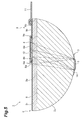
For example, as shown in FIG. 4, the body portion 2 may be formed in such a shape that a semispherical lens is cut out by two flat planes which are approximately orthogonal to the flat plane portion thereof and also approximately parallel with each other. In this instance, the flat plane portion of the semispherical lens is given as the front plane 2 a of the body portion 2, and the spectroscopic portion 3 is formed at a curved portion of the semispherical lens.
Further, as shown in FIG. 5, the body portion 2 may be such that the light-transmitting member 2 1 in a long thin plate shape is pasted to a flat portion of the light-transmitting member 2 2 formed so that the semispherical lens is cut out by two flat planes approximately orthogonal to the flat plane portion thereof and also approximately parallel with each other with the use of an optical resin or by direct bonding. In this instance, the front plane of the light-transmitting member 2 1 is given as the front plane 2 a of the body portion 2, and the spectroscopic portion 3 is formed at a curved portion of the light-transmitting member 2 2.
Still further, as shown in FIG. 6, the light transmitting member 2 3 which acts as a lens may be formed integrally with the diffraction layer 14, for example, by using light-transmitting low-melting point glass for replica molding. Thereby, it is possible to simplify the manufacturing process and also prevent the deviation of a relative positional relationship between the light-transmitting member 2 3 and the diffraction layer 14.
INDUSTRIAL APPLICABILITY
According to the present invention, it is possible to improve the reliability.

Claims (13)

1. A spectroscopy module comprising: a light-transmitting body portion;
a spectroscopic portion for dispersing light made incident from a predetermined plane of the body portion into the body portion, and reflecting the light on the predetermined plane;
the spectroscopic portion is arranged on a plane of the body portion, the plane facing the predetermined plane; and
a light detecting element supported on the predetermined plane to detect the light dispersed and reflected by the spectroscopic portion;
wherein a light absorbing layer having a first light-passing hole through which light advancing to the spectroscopic portion passes and a second light-passing hole through which light advancing to the light detecting element passes is formed on the predetermined plane.
2. The spectroscopy module as set forth in claim 1, wherein the body portion is provided with a plurality of light-transmitting members laminated in a direction approximately orthogonal to the predetermined plane.
3. The spectroscopy module as set forth in claim 2, wherein the light-transmitting members having the predetermined plane are formed in a plate shape.
4. The spectroscopy module as set forth in claim 2, wherein a light absorbing layer is formed between the light-transmitting members adjacent to each other in a direction approximately orthogonal to the predetermined plane.
5. The spectroscopy module as set forth in claim 1, wherein wiring electrically connected to the light detecting element is formed on the predetermined plane,
a wiring is electrically connected to an external terminal of the light detecting element, the external terminal facing the predetermined plane.
6. The spectroscopy module as set forth in claim 5, wherein the wiring is provided with a light absorbing layer on the predetermined plane.
7. The spectroscopy module as set forth in claim 1, wherein the wiring electrically connected to the light detecting element is formed on a plane opposite to the predetermined plane on the light absorbing layer formed on the predetermined plane,
a wiring is electrically connected to an external terminal of the light detecting element, the external terminal facing the predetermined plane.
8. The spectroscopy module as set forth in claim 1, wherein the area of the second light-passing hole is larger than the area of the first light-passing hole.
9. The spectroscopy module as set forth in claim 1, wherein the spectroscopic portion has a diffraction layer formed on the outer surface of the light-transmitting body portion, the outer surface formed in a hemisphere or a curved-surface shape.
10. The spectroscopy module as set forth in claim 1, wherein in a direction perpendicular to the direction along which the second light-passing hole and the first light-passing hole are juxtaposed, the width of the first light-passing hole is larger than the width of the second light-passing hole.
11. The spectroscopy module as set forth in claim 4, wherein the area of the first light-passing hole of the light absorbing layer formed between the light-transmitting members is larger than the area of the first light-passing hole of the light absorbing layer formed on the predetermined plane and the area of the second light-passing hole of the light absorbing layer formed between the light-transmitting members is larger than the area of the second light-passing hole of the light absorbing layer formed on the predetermined plane.
12. The spectroscopy module as set forth in claim 5 or 7, wherein an electrical insulation layer is formed in a film shape between the light absorbing layer and the wiring.
13. The spectroscopy module as set forth in claim 5, wherein a connection portion of the wiring is covered with the light absorbing layer and pad portions of the wiring are exposed from the light absorbing layer.
US12/377,325 2007-06-08 2008-06-05 Spectroscopic module Active US8068224B2 (en)

Applications Claiming Priority (4)

Application Number Priority Date Filing Date Title
JP2007153014A JP4887221B2 (en) 2007-06-08 2007-06-08 Spectroscopic module
JP2007-153014 2007-06-08
JPP2007-153014 2007-06-08
PCT/JP2008/060361 WO2008149928A1 (en) 2007-06-08 2008-06-05 Spectroscopic module

Publications (2)

Publication Number Publication Date
US20100201980A1 US20100201980A1 (en) 2010-08-12
US8068224B2 true US8068224B2 (en) 2011-11-29

Family

ID=40093739

Family Applications (1)

Application Number Title Priority Date Filing Date
US12/377,325 Active US8068224B2 (en) 2007-06-08 2008-06-05 Spectroscopic module

Country Status (7)

Country Link
US (1) US8068224B2 (en)
EP (1) EP2154498B1 (en)
JP (1) JP4887221B2 (en)
KR (1) KR101642514B1 (en)
CN (3) CN101542247B (en)
TW (1) TWI445931B (en)
WO (1) WO2008149928A1 (en)

Cited By (3)

* Cited by examiner, † Cited by third party
Publication number Priority date Publication date Assignee Title
US9714863B2 (en) 2012-11-29 2017-07-25 International Business Machines Corporation Optical spectrometer
US20180259393A1 (en) * 2017-03-10 2018-09-13 Hitachi High-Tech Analytical Science Limited Portable Analyzer Using Optical Emission Spectroscopy
US10775236B2 (en) * 2014-02-05 2020-09-15 Hamamatsu Photonics K.K. Spectrometer, and spectrometer production method

Families Citing this family (16)

* Cited by examiner, † Cited by third party
Publication number Priority date Publication date Assignee Title
JP4891841B2 (en) * 2007-06-08 2012-03-07 浜松ホトニクス株式会社 Spectroscopic module
KR101491889B1 (en) 2007-06-08 2015-02-11 하마마츠 포토닉스 가부시키가이샤 Spectroscope
WO2008149940A1 (en) * 2007-06-08 2008-12-11 Hamamatsu Photonics K.K. Spectroscopic module
JP4887221B2 (en) 2007-06-08 2012-02-29 浜松ホトニクス株式会社 Spectroscopic module
EP2072978A4 (en) * 2007-06-08 2014-01-08 Hamamatsu Photonics Kk Spectroscopic module
JP4891840B2 (en) * 2007-06-08 2012-03-07 浜松ホトニクス株式会社 Spectroscopic module
EP2075555A4 (en) 2007-06-08 2014-01-01 Hamamatsu Photonics Kk Spectroscopic module
JP5207938B2 (en) * 2008-05-15 2013-06-12 浜松ホトニクス株式会社 Spectroscopic module and method for manufacturing spectral module
JP5074291B2 (en) * 2008-05-15 2012-11-14 浜松ホトニクス株式会社 Spectroscopic module
JP2010261767A (en) 2009-05-01 2010-11-18 Canon Inc Spectroscopic device and image forming apparatus with the same
JP5825880B2 (en) * 2011-06-27 2015-12-02 浜松ホトニクス株式会社 Spectroscopic module
JP5910989B2 (en) * 2012-03-09 2016-04-27 株式会社リコー Spectroscopic measurement apparatus, image evaluation apparatus, and image forming apparatus
JP5113947B2 (en) * 2012-04-18 2013-01-09 浜松ホトニクス株式会社 Spectroscopic module
JP6061542B2 (en) * 2012-08-06 2017-01-18 浜松ホトニクス株式会社 Spectrometer
CN107179584B (en) * 2016-03-10 2019-06-14 源杰科技股份有限公司 Optical conenctor
WO2020008851A1 (en) * 2018-07-06 2020-01-09 浜松ホトニクス株式会社 Spectral module and method for manufacturing spectral module

Citations (40)

* Cited by examiner, † Cited by third party
Publication number Priority date Publication date Assignee Title
JPS54143685A (en) 1978-04-29 1979-11-09 Ritsuo Hasumi Compact spectroscope for digital light wavemeter
JPS626126A (en) 1985-07-03 1987-01-13 Shimadzu Corp Sensor for analyzing light spectrum
JPS63229765A (en) 1987-03-18 1988-09-26 Fujitsu Ltd Detector for infrared rays
US4784935A (en) 1986-04-04 1988-11-15 Kernforschungszentrum Karlsruhe Gmbh Method of producing a passive optical device including at least one reflection grating
JPH03119917A (en) 1989-09-30 1991-05-22 Iseki & Co Ltd Grass reaper in mower
US5026160A (en) * 1989-10-04 1991-06-25 The United States Of America As Represented By The Secretary Of The Navy Monolithic optical programmable spectrograph (MOPS)
JPH04294223A (en) 1990-12-04 1992-10-19 Carl Zeiss:Fa Diode-line type spectrochemical analyzer
JPH05322653A (en) 1992-05-26 1993-12-07 Hamamatsu Photonics Kk Semiconductor photosensor
JPH06129908A (en) 1992-10-15 1994-05-13 Hamamatsu Photonics Kk Spectroscopic imaging sensor
JPH06229829A (en) 1993-02-04 1994-08-19 Olympus Optical Co Ltd Photoreceptor element array
JPH08145794A (en) 1994-11-17 1996-06-07 Shimadzu Corp Spectroscope
DE19717015A1 (en) 1997-04-23 1998-10-29 Inst Mikrotechnik Mainz Gmbh Miniaturized optical component and method for its production
WO1999053350A1 (en) 1998-04-10 1999-10-21 Ion Optics, Inc. Monolithic infrared spectrometer apparatus and methods
US6081331A (en) * 1998-03-11 2000-06-27 Gretag-Macbeth Ag Spectrometer
JP2000298066A (en) 1999-04-01 2000-10-24 Gretag Macbeth Ag Spectrometer
US6181418B1 (en) 1998-03-12 2001-01-30 Gretag Macbeth Llc Concentric spectrometer
JP2003139611A (en) 2001-11-06 2003-05-14 Olympus Optical Co Ltd Spectrophotometer
JP2003202463A (en) 2002-01-09 2003-07-18 Fujitsu Ltd Wavelength multiplex bidirectional optical transmission module
JP2003243444A (en) 2002-02-20 2003-08-29 Nippon Telegr & Teleph Corp <Ntt> Substrate mounting structure and semiconductor device
US20030197862A1 (en) 2000-12-13 2003-10-23 Cohen Mitchell S. Multimode planar spectrographs for wavelength demultiplexing and methods of fabrication
JP2003318478A (en) 2002-04-26 2003-11-07 Sumitomo Electric Ind Ltd Optical communication apparatus
JP2003337206A (en) 2001-05-09 2003-11-28 Nippon Sheet Glass Co Ltd Resin erecting lens array and method of making the same
JP2004191246A (en) 2002-12-12 2004-07-08 Matsushita Electric Ind Co Ltd Ruggidness detecting sensor
US20040196458A1 (en) 2003-04-02 2004-10-07 Olympus Corporation Spectrophotometer
US20040239931A1 (en) 2003-05-28 2004-12-02 Hamamatsu Photonics K.K. Photodetector and spectrometer using the same
JP2004537750A (en) 2001-08-02 2004-12-16 アイギス セミコンダクター インコーポレイテッド Tunable optics
US6862092B1 (en) * 1999-01-08 2005-03-01 Ibsen Photonics A/S Spectrometer
JP2005308495A (en) 2004-04-20 2005-11-04 Hamamatsu Photonics Kk Spectroscope and measuring apparatus using the same
JP2006030031A (en) 2004-07-16 2006-02-02 Hamamatsu Photonics Kk Spectroscope
CN1800941A (en) 2005-01-06 2006-07-12 群康科技(深圳)有限公司 Backlight module assembly
US20070252989A1 (en) 2006-04-28 2007-11-01 Comstock Lovell E Monolithic offner spectrometer
US7369228B2 (en) 2003-02-04 2008-05-06 Carl Zeiss Microimaging Gmbh Compact spectrometer
JP4294223B2 (en) 1998-11-09 2009-07-08 ザ ロゴシン インスティチュート Composition of restricted rapid-growable cells producing growth inhibitors and uses thereof
US20100103412A1 (en) 2007-06-08 2010-04-29 Hamamatsu Photonics K.K. Spectroscopic module
US20100201980A1 (en) 2007-06-08 2010-08-12 Hamamatsu Phtonics K.K. Spectroscopic module
US20100208259A1 (en) 2007-06-08 2010-08-19 Hamamatsu Photonics K.K. Spectroscopic module
US20100208257A1 (en) 2007-06-08 2010-08-19 Hamamatsu Photonics K.K. Spectroscopic module
US20100208258A1 (en) 2007-06-08 2010-08-19 Hamamatsu Photonics K.K. Spectroscope
US20100214563A1 (en) 2007-06-08 2010-08-26 Hamamatsu Photonics K.K. Spectroscopic module
US20100238439A1 (en) 2007-06-08 2010-09-23 Tomofumi Suzuki Spectroscopic module

Family Cites Families (1)

* Cited by examiner, † Cited by third party
Publication number Priority date Publication date Assignee Title
US5995221A (en) * 1997-02-28 1999-11-30 Instruments S.A., Inc. Modified concentric spectrograph

Patent Citations (46)

* Cited by examiner, † Cited by third party
Publication number Priority date Publication date Assignee Title
JPS54143685A (en) 1978-04-29 1979-11-09 Ritsuo Hasumi Compact spectroscope for digital light wavemeter
JPS626126A (en) 1985-07-03 1987-01-13 Shimadzu Corp Sensor for analyzing light spectrum
US4784935A (en) 1986-04-04 1988-11-15 Kernforschungszentrum Karlsruhe Gmbh Method of producing a passive optical device including at least one reflection grating
JPS63229765A (en) 1987-03-18 1988-09-26 Fujitsu Ltd Detector for infrared rays
JPH03119917A (en) 1989-09-30 1991-05-22 Iseki & Co Ltd Grass reaper in mower
US5026160A (en) * 1989-10-04 1991-06-25 The United States Of America As Represented By The Secretary Of The Navy Monolithic optical programmable spectrograph (MOPS)
JPH04294223A (en) 1990-12-04 1992-10-19 Carl Zeiss:Fa Diode-line type spectrochemical analyzer
JP3119917B2 (en) 1990-12-04 2000-12-25 カール−ツアイス−スチフツング Diode array spectrometer
JPH05322653A (en) 1992-05-26 1993-12-07 Hamamatsu Photonics Kk Semiconductor photosensor
JPH06129908A (en) 1992-10-15 1994-05-13 Hamamatsu Photonics Kk Spectroscopic imaging sensor
JPH06229829A (en) 1993-02-04 1994-08-19 Olympus Optical Co Ltd Photoreceptor element array
JPH08145794A (en) 1994-11-17 1996-06-07 Shimadzu Corp Spectroscope
US6303934B1 (en) 1997-04-10 2001-10-16 James T. Daly Monolithic infrared spectrometer apparatus and methods
DE19717015A1 (en) 1997-04-23 1998-10-29 Inst Mikrotechnik Mainz Gmbh Miniaturized optical component and method for its production
US6081331A (en) * 1998-03-11 2000-06-27 Gretag-Macbeth Ag Spectrometer
US6181418B1 (en) 1998-03-12 2001-01-30 Gretag Macbeth Llc Concentric spectrometer
WO1999053350A1 (en) 1998-04-10 1999-10-21 Ion Optics, Inc. Monolithic infrared spectrometer apparatus and methods
JP4294223B2 (en) 1998-11-09 2009-07-08 ザ ロゴシン インスティチュート Composition of restricted rapid-growable cells producing growth inhibitors and uses thereof
US6862092B1 (en) * 1999-01-08 2005-03-01 Ibsen Photonics A/S Spectrometer
JP2000298066A (en) 1999-04-01 2000-10-24 Gretag Macbeth Ag Spectrometer
US20030197862A1 (en) 2000-12-13 2003-10-23 Cohen Mitchell S. Multimode planar spectrographs for wavelength demultiplexing and methods of fabrication
JP2003337206A (en) 2001-05-09 2003-11-28 Nippon Sheet Glass Co Ltd Resin erecting lens array and method of making the same
JP2004537750A (en) 2001-08-02 2004-12-16 アイギス セミコンダクター インコーポレイテッド Tunable optics
JP2003139611A (en) 2001-11-06 2003-05-14 Olympus Optical Co Ltd Spectrophotometer
JP2003202463A (en) 2002-01-09 2003-07-18 Fujitsu Ltd Wavelength multiplex bidirectional optical transmission module
JP2003243444A (en) 2002-02-20 2003-08-29 Nippon Telegr & Teleph Corp <Ntt> Substrate mounting structure and semiconductor device
JP2003318478A (en) 2002-04-26 2003-11-07 Sumitomo Electric Ind Ltd Optical communication apparatus
JP2004191246A (en) 2002-12-12 2004-07-08 Matsushita Electric Ind Co Ltd Ruggidness detecting sensor
US7369228B2 (en) 2003-02-04 2008-05-06 Carl Zeiss Microimaging Gmbh Compact spectrometer
US20040196458A1 (en) 2003-04-02 2004-10-07 Olympus Corporation Spectrophotometer
US7092090B2 (en) 2003-04-02 2006-08-15 Olympus Corporation Spectrophotometer
JP2004354176A (en) 2003-05-28 2004-12-16 Hamamatsu Photonics Kk Photodetector and spectrometer using it
US20040239931A1 (en) 2003-05-28 2004-12-02 Hamamatsu Photonics K.K. Photodetector and spectrometer using the same
JP2005308495A (en) 2004-04-20 2005-11-04 Hamamatsu Photonics Kk Spectroscope and measuring apparatus using the same
JP2006030031A (en) 2004-07-16 2006-02-02 Hamamatsu Photonics Kk Spectroscope
US7605917B2 (en) 2004-07-16 2009-10-20 Hamamatsu Photonics K.K. Spectrometer
CN1800941A (en) 2005-01-06 2006-07-12 群康科技(深圳)有限公司 Backlight module assembly
US20070252989A1 (en) 2006-04-28 2007-11-01 Comstock Lovell E Monolithic offner spectrometer
US7697137B2 (en) 2006-04-28 2010-04-13 Corning Incorporated Monolithic Offner spectrometer
US20100103412A1 (en) 2007-06-08 2010-04-29 Hamamatsu Photonics K.K. Spectroscopic module
US20100201980A1 (en) 2007-06-08 2010-08-12 Hamamatsu Phtonics K.K. Spectroscopic module
US20100208259A1 (en) 2007-06-08 2010-08-19 Hamamatsu Photonics K.K. Spectroscopic module
US20100208257A1 (en) 2007-06-08 2010-08-19 Hamamatsu Photonics K.K. Spectroscopic module
US20100208258A1 (en) 2007-06-08 2010-08-19 Hamamatsu Photonics K.K. Spectroscope
US20100214563A1 (en) 2007-06-08 2010-08-26 Hamamatsu Photonics K.K. Spectroscopic module
US20100238439A1 (en) 2007-06-08 2010-09-23 Tomofumi Suzuki Spectroscopic module

Non-Patent Citations (1)

* Cited by examiner, † Cited by third party
Title
F. Reininger, et al., "VIRTIS: Visible Infrared Thermal Imaging Spectrometer for the Rosetta Mission," Proceedings. SPIE, vol. 2819 [Imaging Spectrometry II], Aug. 1996, pp. 66-77.

Cited By (4)

* Cited by examiner, † Cited by third party
Publication number Priority date Publication date Assignee Title
US9714863B2 (en) 2012-11-29 2017-07-25 International Business Machines Corporation Optical spectrometer
US10775236B2 (en) * 2014-02-05 2020-09-15 Hamamatsu Photonics K.K. Spectrometer, and spectrometer production method
US20180259393A1 (en) * 2017-03-10 2018-09-13 Hitachi High-Tech Analytical Science Limited Portable Analyzer Using Optical Emission Spectroscopy
US10876888B2 (en) * 2017-03-10 2020-12-29 Hitachi High-Tech Analytical Science Limited Portable analyzer using optical emission spectroscopy

Also Published As

Publication number Publication date
EP2154498A4 (en) 2013-12-25
TWI445931B (en) 2014-07-21
CN101542249A (en) 2009-09-23
WO2008149928A1 (en) 2008-12-11
EP2154498B1 (en) 2018-08-08
KR20100017085A (en) 2010-02-16
KR101642514B1 (en) 2016-07-25
CN101542247A (en) 2009-09-23
CN101542249B (en) 2012-07-25
CN101542247B (en) 2013-08-21
CN101542252A (en) 2009-09-23
EP2154498A1 (en) 2010-02-17
JP2008304385A (en) 2008-12-18
JP4887221B2 (en) 2012-02-29
US20100201980A1 (en) 2010-08-12
TW200916741A (en) 2009-04-16

Similar Documents

Publication Publication Date Title
US8068224B2 (en) Spectroscopic module
US8411269B2 (en) Spectroscopic module
US8045155B2 (en) Spectroscopic module
US8068223B2 (en) Spectroscopic module
US8049887B2 (en) Spectroscopic module
US8564773B2 (en) Spectroscopy module
KR101735131B1 (en) Spectroscopy module and manufacturing method therefor
US8139214B2 (en) Spectroscopy module, and method for manufacturing the same
US8013993B2 (en) Spectroscopy module
US8018591B2 (en) Spectroscopy module
US8027034B2 (en) Method for manufacturing spectroscopy module, and spectroscopy module
JP4887251B2 (en) Spectroscopic module
JP2009069016A (en) Spectroscopic module
JP5097294B2 (en) Spectroscopic module
JP4980184B2 (en) Spectroscopic module
JP5113947B2 (en) Spectroscopic module

Legal Events

Date Code Title Description
AS Assignment

Owner name: HAMAMATSU PHOTONICS K.K., JAPAN

Free format text: ASSIGNMENT OF ASSIGNORS INTEREST;ASSIGNORS:SHIBAYAMA, KATSUMI;YOKINO, TAKAFUMI;SUZUKI, TOMOFUMI;AND OTHERS;SIGNING DATES FROM 20090120 TO 20090126;REEL/FRAME:022251/0918

STCF Information on status: patent grant

Free format text: PATENTED CASE

FPAY Fee payment

Year of fee payment: 4

MAFP Maintenance fee payment

Free format text: PAYMENT OF MAINTENANCE FEE, 8TH YEAR, LARGE ENTITY (ORIGINAL EVENT CODE: M1552); ENTITY STATUS OF PATENT OWNER: LARGE ENTITY

Year of fee payment: 8

MAFP Maintenance fee payment

Free format text: PAYMENT OF MAINTENANCE FEE, 12TH YEAR, LARGE ENTITY (ORIGINAL EVENT CODE: M1553); ENTITY STATUS OF PATENT OWNER: LARGE ENTITY

Year of fee payment: 12