US8072073B2 - Semiconductor device and method of manufacturing same - Google Patents
Semiconductor device and method of manufacturing same Download PDFInfo
- Publication number
- US8072073B2 US8072073B2 US12/210,702 US21070208A US8072073B2 US 8072073 B2 US8072073 B2 US 8072073B2 US 21070208 A US21070208 A US 21070208A US 8072073 B2 US8072073 B2 US 8072073B2
- Authority
- US
- United States
- Prior art keywords
- wiring
- layer
- wiring structure
- insulating layer
- wiring layer
- Prior art date
- Legal status (The legal status is an assumption and is not a legal conclusion. Google has not performed a legal analysis and makes no representation as to the accuracy of the status listed.)
- Expired - Fee Related, expires
Links
Images


Classifications
-
- H—ELECTRICITY
- H01—ELECTRIC ELEMENTS
- H01L—SEMICONDUCTOR DEVICES NOT COVERED BY CLASS H10
- H01L23/00—Details of semiconductor or other solid state devices
- H01L23/52—Arrangements for conducting electric current within the device in operation from one component to another, i.e. interconnections, e.g. wires, lead frames
- H01L23/522—Arrangements for conducting electric current within the device in operation from one component to another, i.e. interconnections, e.g. wires, lead frames including external interconnections consisting of a multilayer structure of conductive and insulating layers inseparably formed on the semiconductor body
- H01L23/528—Geometry or layout of the interconnection structure
- H01L23/5283—Cross-sectional geometry
-
- H—ELECTRICITY
- H01—ELECTRIC ELEMENTS
- H01L—SEMICONDUCTOR DEVICES NOT COVERED BY CLASS H10
- H01L23/00—Details of semiconductor or other solid state devices
- H01L23/52—Arrangements for conducting electric current within the device in operation from one component to another, i.e. interconnections, e.g. wires, lead frames
- H01L23/522—Arrangements for conducting electric current within the device in operation from one component to another, i.e. interconnections, e.g. wires, lead frames including external interconnections consisting of a multilayer structure of conductive and insulating layers inseparably formed on the semiconductor body
- H01L23/532—Arrangements for conducting electric current within the device in operation from one component to another, i.e. interconnections, e.g. wires, lead frames including external interconnections consisting of a multilayer structure of conductive and insulating layers inseparably formed on the semiconductor body characterised by the materials
- H01L23/5329—Insulating materials
-
- H—ELECTRICITY
- H01—ELECTRIC ELEMENTS
- H01L—SEMICONDUCTOR DEVICES NOT COVERED BY CLASS H10
- H01L23/00—Details of semiconductor or other solid state devices
- H01L23/52—Arrangements for conducting electric current within the device in operation from one component to another, i.e. interconnections, e.g. wires, lead frames
- H01L23/522—Arrangements for conducting electric current within the device in operation from one component to another, i.e. interconnections, e.g. wires, lead frames including external interconnections consisting of a multilayer structure of conductive and insulating layers inseparably formed on the semiconductor body
- H01L23/532—Arrangements for conducting electric current within the device in operation from one component to another, i.e. interconnections, e.g. wires, lead frames including external interconnections consisting of a multilayer structure of conductive and insulating layers inseparably formed on the semiconductor body characterised by the materials
- H01L23/53204—Conductive materials
- H01L23/53209—Conductive materials based on metals, e.g. alloys, metal silicides
- H01L23/53214—Conductive materials based on metals, e.g. alloys, metal silicides the principal metal being aluminium
- H01L23/53223—Additional layers associated with aluminium layers, e.g. adhesion, barrier, cladding layers
-
- H—ELECTRICITY
- H01—ELECTRIC ELEMENTS
- H01L—SEMICONDUCTOR DEVICES NOT COVERED BY CLASS H10
- H01L23/00—Details of semiconductor or other solid state devices
- H01L23/52—Arrangements for conducting electric current within the device in operation from one component to another, i.e. interconnections, e.g. wires, lead frames
- H01L23/522—Arrangements for conducting electric current within the device in operation from one component to another, i.e. interconnections, e.g. wires, lead frames including external interconnections consisting of a multilayer structure of conductive and insulating layers inseparably formed on the semiconductor body
- H01L23/532—Arrangements for conducting electric current within the device in operation from one component to another, i.e. interconnections, e.g. wires, lead frames including external interconnections consisting of a multilayer structure of conductive and insulating layers inseparably formed on the semiconductor body characterised by the materials
- H01L23/53204—Conductive materials
- H01L23/53209—Conductive materials based on metals, e.g. alloys, metal silicides
- H01L23/53228—Conductive materials based on metals, e.g. alloys, metal silicides the principal metal being copper
- H01L23/53238—Additional layers associated with copper layers, e.g. adhesion, barrier, cladding layers
-
- H—ELECTRICITY
- H01—ELECTRIC ELEMENTS
- H01L—SEMICONDUCTOR DEVICES NOT COVERED BY CLASS H10
- H01L24/00—Arrangements for connecting or disconnecting semiconductor or solid-state bodies; Methods or apparatus related thereto
- H01L24/01—Means for bonding being attached to, or being formed on, the surface to be connected, e.g. chip-to-package, die-attach, "first-level" interconnects; Manufacturing methods related thereto
- H01L24/02—Bonding areas ; Manufacturing methods related thereto
- H01L24/04—Structure, shape, material or disposition of the bonding areas prior to the connecting process
- H01L24/05—Structure, shape, material or disposition of the bonding areas prior to the connecting process of an individual bonding area
-
- H—ELECTRICITY
- H01—ELECTRIC ELEMENTS
- H01L—SEMICONDUCTOR DEVICES NOT COVERED BY CLASS H10
- H01L2924/00—Indexing scheme for arrangements or methods for connecting or disconnecting semiconductor or solid-state bodies as covered by H01L24/00
- H01L2924/0001—Technical content checked by a classifier
- H01L2924/00013—Fully indexed content
-
- H—ELECTRICITY
- H01—ELECTRIC ELEMENTS
- H01L—SEMICONDUCTOR DEVICES NOT COVERED BY CLASS H10
- H01L2924/00—Indexing scheme for arrangements or methods for connecting or disconnecting semiconductor or solid-state bodies as covered by H01L24/00
- H01L2924/01—Chemical elements
- H01L2924/01019—Potassium [K]
-
- H—ELECTRICITY
- H01—ELECTRIC ELEMENTS
- H01L—SEMICONDUCTOR DEVICES NOT COVERED BY CLASS H10
- H01L2924/00—Indexing scheme for arrangements or methods for connecting or disconnecting semiconductor or solid-state bodies as covered by H01L24/00
- H01L2924/01—Chemical elements
- H01L2924/01057—Lanthanum [La]
-
- H—ELECTRICITY
- H01—ELECTRIC ELEMENTS
- H01L—SEMICONDUCTOR DEVICES NOT COVERED BY CLASS H10
- H01L2924/00—Indexing scheme for arrangements or methods for connecting or disconnecting semiconductor or solid-state bodies as covered by H01L24/00
- H01L2924/01—Chemical elements
- H01L2924/01078—Platinum [Pt]
-
- H—ELECTRICITY
- H01—ELECTRIC ELEMENTS
- H01L—SEMICONDUCTOR DEVICES NOT COVERED BY CLASS H10
- H01L2924/00—Indexing scheme for arrangements or methods for connecting or disconnecting semiconductor or solid-state bodies as covered by H01L24/00
- H01L2924/01—Chemical elements
- H01L2924/01079—Gold [Au]
-
- H—ELECTRICITY
- H01—ELECTRIC ELEMENTS
- H01L—SEMICONDUCTOR DEVICES NOT COVERED BY CLASS H10
- H01L2924/00—Indexing scheme for arrangements or methods for connecting or disconnecting semiconductor or solid-state bodies as covered by H01L24/00
- H01L2924/013—Alloys
- H01L2924/0132—Binary Alloys
- H01L2924/01322—Eutectic Alloys, i.e. obtained by a liquid transforming into two solid phases
-
- H—ELECTRICITY
- H01—ELECTRIC ELEMENTS
- H01L—SEMICONDUCTOR DEVICES NOT COVERED BY CLASS H10
- H01L2924/00—Indexing scheme for arrangements or methods for connecting or disconnecting semiconductor or solid-state bodies as covered by H01L24/00
- H01L2924/10—Details of semiconductor or other solid state devices to be connected
- H01L2924/11—Device type
- H01L2924/12—Passive devices, e.g. 2 terminal devices
- H01L2924/1204—Optical Diode
- H01L2924/12044—OLED
-
- H—ELECTRICITY
- H01—ELECTRIC ELEMENTS
- H01L—SEMICONDUCTOR DEVICES NOT COVERED BY CLASS H10
- H01L2924/00—Indexing scheme for arrangements or methods for connecting or disconnecting semiconductor or solid-state bodies as covered by H01L24/00
- H01L2924/10—Details of semiconductor or other solid state devices to be connected
- H01L2924/11—Device type
- H01L2924/13—Discrete devices, e.g. 3 terminal devices
- H01L2924/1304—Transistor
- H01L2924/1306—Field-effect transistor [FET]
- H01L2924/13091—Metal-Oxide-Semiconductor Field-Effect Transistor [MOSFET]
-
- H—ELECTRICITY
- H01—ELECTRIC ELEMENTS
- H01L—SEMICONDUCTOR DEVICES NOT COVERED BY CLASS H10
- H01L2924/00—Indexing scheme for arrangements or methods for connecting or disconnecting semiconductor or solid-state bodies as covered by H01L24/00
- H01L2924/10—Details of semiconductor or other solid state devices to be connected
- H01L2924/11—Device type
- H01L2924/14—Integrated circuits
-
- H—ELECTRICITY
- H01—ELECTRIC ELEMENTS
- H01L—SEMICONDUCTOR DEVICES NOT COVERED BY CLASS H10
- H01L2924/00—Indexing scheme for arrangements or methods for connecting or disconnecting semiconductor or solid-state bodies as covered by H01L24/00
- H01L2924/19—Details of hybrid assemblies other than the semiconductor or other solid state devices to be connected
- H01L2924/1901—Structure
- H01L2924/1904—Component type
- H01L2924/19041—Component type being a capacitor
-
- H—ELECTRICITY
- H01—ELECTRIC ELEMENTS
- H01L—SEMICONDUCTOR DEVICES NOT COVERED BY CLASS H10
- H01L2924/00—Indexing scheme for arrangements or methods for connecting or disconnecting semiconductor or solid-state bodies as covered by H01L24/00
- H01L2924/19—Details of hybrid assemblies other than the semiconductor or other solid state devices to be connected
- H01L2924/1901—Structure
- H01L2924/1904—Component type
- H01L2924/19042—Component type being an inductor
-
- H—ELECTRICITY
- H01—ELECTRIC ELEMENTS
- H01L—SEMICONDUCTOR DEVICES NOT COVERED BY CLASS H10
- H01L2924/00—Indexing scheme for arrangements or methods for connecting or disconnecting semiconductor or solid-state bodies as covered by H01L24/00
- H01L2924/19—Details of hybrid assemblies other than the semiconductor or other solid state devices to be connected
- H01L2924/1901—Structure
- H01L2924/1904—Component type
- H01L2924/19043—Component type being a resistor
-
- H—ELECTRICITY
- H01—ELECTRIC ELEMENTS
- H01L—SEMICONDUCTOR DEVICES NOT COVERED BY CLASS H10
- H01L2924/00—Indexing scheme for arrangements or methods for connecting or disconnecting semiconductor or solid-state bodies as covered by H01L24/00
- H01L2924/30—Technical effects
- H01L2924/301—Electrical effects
- H01L2924/30105—Capacitance
-
- H—ELECTRICITY
- H01—ELECTRIC ELEMENTS
- H01L—SEMICONDUCTOR DEVICES NOT COVERED BY CLASS H10
- H01L2924/00—Indexing scheme for arrangements or methods for connecting or disconnecting semiconductor or solid-state bodies as covered by H01L24/00
- H01L2924/30—Technical effects
- H01L2924/301—Electrical effects
- H01L2924/30107—Inductance
-
- H—ELECTRICITY
- H01—ELECTRIC ELEMENTS
- H01L—SEMICONDUCTOR DEVICES NOT COVERED BY CLASS H10
- H01L2924/00—Indexing scheme for arrangements or methods for connecting or disconnecting semiconductor or solid-state bodies as covered by H01L24/00
- H01L2924/30—Technical effects
- H01L2924/301—Electrical effects
- H01L2924/3011—Impedance
Definitions
- This invention relates to a semiconductor device and to a method of manufacturing the device. More particularly, the invention relates to a semiconductor device having a high reliability in the form of a package in which the semiconductor device has been connected to a mounting substrate, and to a method of manufacturing this device.
- a low-k material in which the specific inductivity is 2.5 or below, is now being employed in semiconductor devices. Further, lead-free solder materials are now being employed as the material of solder balls in view of effects upon the environment.
- a low-k material has a mechanical strength, such as hardness and elastic modulus, lower than that of silicon oxide, silicon nitride and silicon oxonitride, etc., which have been used heretofore as silicon-based elements.
- a lead-free solder material in comparison with the conventional Pb—Sn eutectic solder material, has a poor creep characteristic. The creep characteristic indicates the ease of deformation of a material. Consequently, the amount of deformation of solder balls per se following the hardening thereof is small and residual stress within the solder balls is large.
- a semiconductor chip is mounted on a mounting substrate such as a printed board or built-up substrate and is used as a semiconductor device (package).
- a semiconductor device such as a printed board or built-up substrate
- FCBGA Flipchip Ball Grid Array
- wafer-level CSP Chip-Size Package
- Various techniques are used to mitigate thermal stress in these packages.
- Patent Document 1 discloses a technique for connecting a semiconductor chip to a BGA substrate using a solder bump and filling the device with an underfill resin in order to protect the small solder-bump connection.
- Patent Document 1 it is possible to provide a highly reliable semiconductor device having a BGA structure in which severance at the solder bump and exfoliation of the semiconductor chip do not occur even if thermal stress is produced by thermal expansion.
- Patent Document 2 discloses a technique for providing a layer having a low elastic modulus on a semiconductor chip and providing an external electrode terminal on this layer.
- stress that acts upon metal balls can be mitigated by thus providing the layer having the low elastic modulus below the metal balls.
- by providing the surface of the semiconductor chip with the metal balls spaced far away from the pads stress produced in the metal balls can be prevented from propagating to the semiconductor chip connected to the pads.
- Patent Document 3 discloses a technique for directly providing a semiconductor element with a wiring layer for the purpose of furnishing a connection reliability greater than that of an FCBGA.
- a resin substrate having a highly rigid core material is provided for an external terminal in a semiconductor device incorporating a semiconductor chip, thereby improving the long-term reliability of the package.
- Patent Document 1 Japanese Patent Kokai Publication No. JP-A-11-74417
- Patent Document 2 Japanese Patent Kokai Publication No. JP-A-11-204560
- Patent Document 3 Japanese Patent Kokai Publication No. JP-P2002-246500A
- Patent Document 4 Japanese Patent Kokai Publication No. JP-A-10-51105
- Patent Document 5 Japanese Patent Kokai Publication No. JP-A-9-64493
- Patent Document 6 Japanese Patent Kokai Publication No. JP-A-6-334334
- Patent Documents 1-6 are incorporated herein by reference thereto. The following analyses are given by the present inventor.
- the via structure in Patent Document 1 is one in which the connection interface with the vias is located in a region where stress concentrates.
- connection interface with the vias is situated at the boundary between the wiring and vias on the side of the semiconductor substrate where there is a large concentration of stress.
- a semiconductor device comprising: a semiconductor substrate; a first wiring structure placed on the semiconductor substrate and having one or more first wiring layers, one or more insulating layers and a first via; a second wiring structure placed on the first wiring structure and having one or more second wiring layers, one or more second insulating layers, a second via and a third via; and an external terminal provided on the second wiring structure; wherein the second via, which is connected to the second wiring layer of the second wiring structure and to the external terminal, has a connection interface disposed at an end of the second via that is on the side of the external terminal.
- a method of manufacturing a semiconductor device comprising: forming a first wiring structure, which has a first insulating layer, a first wiring layer and a first via, on a semiconductor substrate on which semiconductor elements have been formed; forming a second wiring structure, which has a second insulating layer, a second wiring layer, a second via and a third via, on the first wiring structure; and forming an external terminal on the second wiring structure; wherein the forming the second wiring structure includes: forming the second wiring layer; forming a metal post, which will serve as the second via, on the second wiring layer; covering the second wiring layer and the metal post with the second insulating layer; and exposing the metal post by polishing the surface of the second insulating layer.
- the second wiring structure comprising thick insulating and wiring layers and the very small first wiring structure can be protected.
- the second wiring structure which is obtained by building up the second insulating layers and second wiring layers thicker than the insulating and wiring layers of the first wiring structure using an organic resin as the insulating layers, is provided on the first wiring structure obtained by building up the first wiring layers and first insulating layers alternatingly on the semiconductor substrate.
- the amounts of deformation and migration in the respective layers of the plurality of wiring layers, as well as the directions thereof, differ depending upon the shapes and thicknesses of the respective layers and the areas of adhesion to the insulating layers, and stress concentrates at the vias connecting the external electrodes and the wiring layers.
- a connection interface is provided in the area on the side of the external terminals and not at the boundary with the wiring layer on the side of the semiconductor substrate, and the insulating layers and wiring layers, inclusive of the region of the connection interface, are made to adhere.
- the insulating layers are corrected by the wiring layers and similar deformation occurs in the area of adhesion that includes the connection interface with the vias.
- This effect manifests itself in particular with regard to a via diameter of less than 20 ⁇ m. Accordingly, it is possible to provide a highly reliable semiconductor device that operates with a large driving current and at a high frequency.
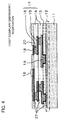
- FIG. 1 is a partial sectional view schematically illustrating the configuration of a semiconductor device according to a first exemplary embodiment of the present invention
- FIG. 2 is an enlarged partial sectional view schematically illustrating the configuration of a first wiring structure in the semiconductor device according to the first exemplary embodiment
- FIGS. 3A and 3B are enlarged partial sectional views useful in describing concentration of stress in a second wiring structure in the semiconductor device according to the first exemplary embodiment
- FIG. 4 is a partial sectional view schematically illustrating the configuration of a first modification of the semiconductor device according to the first exemplary embodiment
- FIG. 5 is a partial sectional view schematically illustrating the configuration of a second modification of the semiconductor device according to the first exemplary embodiment
- FIGS. 6A to 6C are schematic views illustrating an example of the effects of a reduction in external terminals in the semiconductor device according to the first exemplary embodiment
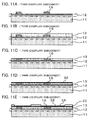
- FIGS. 7A to 7E are first process sectional views schematically illustrating a method of manufacturing a semiconductor device according to the first exemplary embodiment
- FIGS. 8A to 8D are second process sectional views schematically illustrating a method of manufacturing a semiconductor device according to the first exemplary embodiment
- FIG. 9 is a partial sectional view schematically illustrating the configuration of a semiconductor device according to a second exemplary embodiment of the present invention.
- FIG. 10 is a partial sectional view schematically illustrating the configuration of a semiconductor device according to a third exemplary embodiment of the present invention.
- FIGS. 11A to 11E are first process sectional views schematically illustrating a method of manufacturing a semiconductor device according to the third exemplary embodiment.
- FIGS. 12A to 12E are second process sectional views schematically illustrating a method of manufacturing a semiconductor device according to the third exemplary embodiment.
- a semiconductor device comprises: a semiconductor substrate 11 ( FIG. 1 ); a first wiring structure 12 ( FIG. 1 ) placed on the semiconductor substrate 11 ( FIG. 1 ) and having one or more first wiring layers 26 ( FIG. 2 ), one or more insulating layers 27 ( FIG. 2 ) and a first via 30 ( FIG. 2 ); a second wiring structure 17 ( FIG. 1 ) placed on the first wiring structure 12 ( FIG. 1 ) and having one or more second wiring layers 15 ( FIG. 1 ), one or more second insulating layers 14 ( FIG. 1 ), a second via 16 ( FIG. 1 ) and a third via 19 ( FIG. 1 ); and an external terminal 18 ( FIG. 1 ) provided on the second wiring structure 17 ( FIG. 1 ).
- the second via 16 ( FIG. 1 ), which is connected to the second wiring layer 15 ( FIG. 1 ) of the second wiring structure 17 ( FIG. 1 ) and to the external terminal 18 ( FIG. 1 ), has a connection interface 16 a ( FIG. 1 ) disposed at an end of the second via that is on the side of the external terminal 18 ( FIG. 1 ).
- a method of manufacturing a semiconductor device comprises: forming a first wiring structure 12 ( FIG. 7 ), which has a first insulating layer, a first wiring layer and a first via, on a semiconductor substrate 11 ( FIG. 7A ) on which semiconductor elements have been formed; forming a second wiring structure 17 ( FIG. 8D ), which has a second insulating layer 14 ( FIG. 8D ), a second wiring layer 15 ( FIG. 8D ), a second via 16 ( FIG. 8D ) and a third via 19 ( FIG. 8D ), on the first wiring structure 12 ( FIG. 7A ); and forming an external terminal 18 ( FIG. 8D ) on the second wiring structure 17 ( FIG. 8D ).
- the forming the second wiring structure 17 ( FIG. 7 ) which has a first insulating layer, a first wiring layer and a first via, on a semiconductor substrate 11 ( FIG. 7A ) on which semiconductor elements have been formed
- 8D includes: forming the second wiring layer (which corresponds to electroplating 34 in FIG. 7D ); forming a metal post 36 ( FIG. 8A ), which will serve as the second via 16 ( FIG. 8 ), on the second wiring layer 15 ( FIG. 8A ); covering the second wiring layer 15 ( FIG. 8B ) and the metal post 36 ( FIG. 8B ) with the second insulating layer 14 ( FIG. 8B ); and exposing the metal post (which corresponds to the second via 16 in FIG. 8C ) by polishing the surface of the second insulating layer 14 ( FIG. 8C ).
- FIG. 1 is a partial sectional view schematically illustrating the configuration of a semiconductor device according to a first exemplary embodiment of the present invention
- FIG. 2 is an enlarged partial sectional view schematically illustrating the configuration of a first wiring structure in the semiconductor device according to the first exemplary embodiment.
- the first wiring structure 12 includes source electrodes 22 and drain electrodes 23 formed alternatingly in space-apart relation on the surface of the semiconductor substrate 11 .
- a gate electrode 21 is formed via a gate insulating film (not shown) on a channel region delimited by diffusion areas 22 and 23 (for example, the source electrode 22 and drain electrode 23 ).
- a MOS (Metal Oxide Semiconductor) transistor 24 is constructed by the gate electrode 21 , source electrode 22 and drain electrode 23 .
- a plurality of the MOS transistors 24 are provided on the semiconductor substrate 11 .
- a first insulating layer 27 covered by an insulating film 29 is formed on the MOS transistors 24 and on the surface of the semiconductor substrate 11 . Plugs 25 connected to the source electrode 22 and drain electrode 23 are formed on the first insulating layer 27 on semiconductor substrate 11 .
- a first wiring layer 26 is provided on the first insulating layer 27 .
- the first wiring layer 26 is composed of wiring 28 and the insulating film 29 .
- the wiring 28 is electrically connected to respective ones of the source electrode 22 and drain electrode 23 by the plugs 25 formed in the first insulating layer 27 .
- the first insulating layer 27 is provided on the first wiring layer 26
- the first wiring layer 26 is provided on the first insulating layer 27 .
- the first insulating layer 27 is composed of the insulating film 29 and a first via 30 .
- the wiring 28 of the first wiring layers 26 above and below the first insulating layer 27 is electrically connected by the corresponding first via 30 .
- the first wiring structure 12 is constructed by building up the first insulating layers 27 and first wiring layers 26 alternatingly.
- the wiring 28 and first via 30 of the first wiring structure 12 mainly comprise copper or aluminum, by way of example, and can be formed by, e.g., the damascene method.
- the damascene method forms a trench in the shape of a desired wiring pattern or via pattern in an insulating film by dry etching, provides a barrier metal by a sputtering method, CVD (Chemical Vapor Deposition) method or ALD (Atomic Layer Deposition) method, etc., then forms a feed layer (not shown), which is for electroplating, by a sputtering method, etc., fills the trench with copper by copper electroplating and then applies a CMP (Chemical Mechanical Polishing) method which leaves the copper only in the trench, thereby providing the desired wiring.
- CVD Chemical Vapor Deposition
- ALD Atomic Layer Deposition
- the thickness of the first insulating layer 27 is 0.2 to 1.6 ⁇ m, by way of example. Further, among the plurality of first insulating layers 27 , at least one first insulating layer 27 provided near the semiconductor substrate 11 preferably uses a low-k material. By way of example, a porous silicon oxide film is used as the low-k material and the elastic modulus thereof at 25° C. is 4 to 10 GPa.
- an insulating passivation film 13 comprising an inorganic or organic material is provided on the first wiring structure 12 , and a second wiring layer 15 and second insulating layer 14 are provided on the passivation film.
- the second wiring layer 15 and wiring 28 (see FIG. 2 ) on the surface of the first wiring structure 12 are electrically connected via a third via 19 .
- the second wiring structure 17 is constructed by building up the second insulating layers 14 and second wiring layers 15 alternatingly.
- the plurality of second wiring layers 15 are electrically connected by a second via 16 .
- An external terminal 18 is provided on the second insulating layer 14 that is the uppermost layer.
- the external terminal 18 is electrically connected to the second wiring layer 15 through the corresponding second via 16 .
- the external terminal 18 may have such a structure that the position thereof is changed depending upon the surface-layer wiring in conformity with the connection method, or such a structure that the terminal is provided directly on the second via 16 .
- the second wiring layer 15 consists of, e.g., copper, and can have a thickness of 5 ⁇ m.
- the second wiring layer 15 is formed by a wiring formation method different from that of the first wiring structure 12 , e.g., a subtractive method, a semi-additive method or a full-additive method.
- the subtractive method subjects a copper foil, which has been provided on a substrate or resin, to etching using a resist, which has been formed into a desired pattern, as an etching mask, then removes the resist to obtain the desired wiring pattern.
- the semi-additive method forms a feed layer by non-electrolytic plating, a sputtering method or CVD method, etc., then forms a resist having openings into a desired pattern, deposits an electroplating metal in the openings of the resist by electrolysis, removes the resist and then etches the feed layer to obtain the desired wiring pattern.
- the full-additive method causes a non-electrolytic plating catalyst to be adsorbed onto the surface of a substrate or resin, then forms a pattern by a resist, activates the catalyst leaving the resist as an insulating layer and deposits a metal in the opening of the insulating layer by a non-electrolytic plating method, thereby obtaining the desired wiring pattern.
- the surface of the passivation film 13 or second insulating layer 14 may be a roughened surface having fine unevenness, in which case good adhesion is readily obtained even with copper or aluminum. Formation of the layer by sputtering is ideal as means for improving adhesion.
- the second insulating layer 14 inclusive of the periphery of the second via is corrected by the external terminal 18 or second wiring layer 15 .
- the external terminal 18 at the periphery of the adhesion layer 37 and the second wiring layer 15 , second via 16 and second insulating layer 14 therefore move in approximately the same direction.
- the connection interface between the second via 16 and the external terminal 18 or second wiring layer 15 undergoes little deformation and breakage at the connection interface can be prevented effectively even with the second via 16 of very small diameter.
- the second wiring layer 15 is formed thicker than the first wiring layer 26 ( FIG. 2 ) of the first wiring structure 12 .
- the thickness of the second wiring layer 15 is, e.g., 3 to 12 ⁇ m, preferably 5 to 10 ⁇ m. If the thickness is less than 3 ⁇ m, the wiring resistance will be high and the electrical characteristics of the power supply circuit of the semiconductor device will deteriorate.
- a wiring layer whose thickness exceeds 12 ⁇ m will produce waviness, which reflects the unevenness of the wiring layer, in the surface of the insulating layer that covers the wiring layer, limits the number of layers built up, increases the thickness of the second wiring structure 17 per se, enlarges the warpage of the overall semiconductor device and makes formation difficult owing to process-related limitations.
- the second insulating layer 14 is formed from, e.g., an organic material.
- organic material examples are epoxy resin, epoxy acrylate resin, urethane acrylate resin, polyester resin, phenol resin, polyimide resin, BCB (benzocyclobutene), PBO (polybenzoxazole) and polynorbornene resin, etc.
- polyimide resin and PBO excel in such mechanical characteristics as film strength, tensile elastic modulus and breakage elongation and therefore can furnish high reliability. It does not matter whether the organic material is photosensitive or non-photosensitive.
- the elastic modulus of the second insulating layer 14 at 25° C. is, e.g., 0.15 to 8 GPa. If the elastic modulus is less than 0.15 GPa, the amount of deformation of the second insulating layer 14 when stress is mitigated is large, almost all of the stress is impressed upon the second wiring layer 15 , the second wiring layer 15 is readily severed and breakage readily occurs at the interface of the second wiring layer 15 /second via 16 . If the elastic modulus exceeds 8 GPa, the amount of deformation of the second insulating layer 14 is too small, mitigation of stress in the second wiring structure 17 is unsatisfactory and exfoliation between layers and destruction of the insulating film readily occur in the first wiring structure 12 .
- an elastic modulus of 0.15 to 8 GPa is preferred. Further, by adopting a combination in which the elastic modulus of the second insulating layer 14 of second wiring structure 17 is lower than that of the first insulating layer 27 ( FIG. 2 ) of first wiring structure 12 , stress is mitigated effectively by the second insulating layer 14 and the first wiring structure 12 can be protected.
- the breakage elongation of the second insulating layer 14 is equal to or greater than 15%. If the breakage elongation is less than 15%, cracks readily develop in the second insulating layer 14 . For example, when the semiconductor device according to the first exemplary embodiment was mounted on a mounting substrate and subjected to a temperature cycle test at ⁇ 55 to 125° C., cracks were produced in the second insulating layer 14 by 100 to 300 cycles. Accordingly, it is preferred that the breakage elongation be equal to or greater than 15%.
- the coefficient of thermal expansion be less than 40 ppm/° C. If the coefficient of thermal expansion exceeds 40 ppm/° C., the wafer that forms the semiconductor device will warp owing to internal stress of the second insulating layer 14 . In a silicon wafer having a diameter of 200 mm (8 inches) and a thickness of 0.725 mm, this amount of warpage exceeds 200 ⁇ m in a case where the thickness of the overall insulating layer is in the vicinity of 30 to 35 ⁇ m.
- the deformation of the second insulating layer 14 having a low elastic modulus deforms more than the highly rigid second wiring layer 15 and stress concentrates at the second via 16 connecting a plurality of the second wiring layers 15 .
- This concentration of stress is as illustrated in FIGS. 3A and 3B .
- the stand-alone state shown in FIG. 3A becomes the state shown in FIG. 3B , in which external stress indicated by the arrow is received. Under this condition of received external stress, the direction of deformation and amount thereof in each layer vary owing to a difference in the patterns of the external terminal 18 and second wiring layer 15 .
- the second insulating layer 14 is strongly joined to the external terminal 18 or to second wiring layer 15 by the adhesion layers 37 , wiring correction areas 38 shown in FIGS. 3A , 3 B are produced in the second insulating layer 14 .
- the second insulating layer 14 has its deformation corrected by the external terminal 18 or second wiring layer 15 and the deformation follows the respective patterns. As a result, stress does not concentrate at the connection interface of the second via 16 .
- connection reliability can be improved at a second via 16 having a diameter of less than 20 ⁇ m.
- the adhesion layer 37 does not exist and the second wiring layer 15 and second via 16 are integrated.
- the fact that there is no interface that invites breakage at the stress concentration area 39 is ideal. Also ideal is that grain boundary of the material constituting the second wiring layer 15 and second via 16 is not provided so as to cross the second via 16 in a plane in the stress concentration area 39 .
- connection interface 16 a of the second via 16 In order to place the connection interface 16 a of the second via 16 on the side of the external terminal, use is made of a method of forming a post at the position of the second via 16 beforehand by a plating method or forming the post and wiring by performing etching after full-surface plating, then forming an insulating film of an organic material, polishing and exposing the post to thereby obtain the second via 16 .
- the plating method the oxide on the surface of the underlying metal is removed by a pre-treatment, and epitaxial growth that follows the grain boundary of the underlying metal occurs when the initial deposition of plating metal is performed.
- the second wiring layer 15 and second via 16 finally constructed become an integrated whole even though the process is divided. This makes it possible to avoid a state in which the grain boundary crosses the plane.
- the external terminal 18 may have the structures shown in FIGS. 4 and 5 .
- FIG. 4 if connection is achieved using a solder material, an opening is limited by an overcoat film 20 so as to obtain a state in which solder is supplied solely to the external terminal 18 . Since the amount of solder flow is limited owing to the limitation applied by the overcoat film 20 , it is possible to stabilize mounting height when the semiconductor device is mounted on the mounting substrate.
- the second via 16 for making the connection to the external terminal 18 is exposed in the opening of the overcoat film 20 , and the external terminal 18 is provided so as to cover the exposed portion of the second via 16 and the opening in the overcoat film 20 .
- the overcoat film 20 is formed from, e.g., epoxy resin, epoxy acrylate resin, urethane acrylate resin, polyester resin, phenol resin, polyimide resin, BCB (benzocyclobutene), PBO (polybenzoxazole) and polynorbornene resin, etc.
- polyimide resin and PBO excel in such mechanical characteristics as film strength, tensile elastic modulus and breakage elongation and therefore can furnish high reliability. It does not matter whether the organic material is photosensitive or non-photosensitive.
- the opening in the overcoat film 20 is formed by photolithography or the like.
- the opening in the overcoat film 20 is formed by laser, dry etching or blasting, etc.
- the surface of the external terminal 18 can be formed by at least one metal selected from the group comprising, e.g., copper, aluminum, gold, silver and solder material, or an alloy thereof, taking into consideration the wetness of solder balls formed on the surface of the external terminal 18 and the connectivity of bonding wires, etc.
- the external terminal 18 can be constructed by building up a plurality of layers. For example, a nickel layer and a gold layer can be built up on a copper layer, the gold layer can be adopted as the surface, and the thicknesses of the nickel layer and gold layer can be made 3 ⁇ m and 1 ⁇ m, respectively.
- the second insulating layer 14 and the second wiring layer 15 are illustrated as two layers each. However, this does not impose a limitation and the number of layers used may decided as necessary. Further, in FIG. 2 , there are eight layers of the first wiring layer 26 and seven layers of the first insulating layer 27 . However, this does not impose a limitation and the number of layers used may decided as necessary.
- the wiring of the first wiring layer 26 and second wiring layer 15 is composed of at least one metal selected from the group comprising, e.g., copper, aluminum, nickel, gold and silver.
- copper is ideal from the standpoints of electrical resistance value and cost.
- nickel makes it possible to prevent an interfacial reaction with another material such as the insulating material and can be used as an inductor or resistance wiring that exploits the characteristics of a magnetic material.
- the thickness of the second wiring layer 15 of second wiring structure 17 is two or more times the thickness of the first wiring layer 26 of first wiring structure 12 , and therefore it has an allowable amount of current that is at least two or more times greater.
- a plurality of power wires or ground wires using identical voltage can be bundled together into a single wire.
- the result is as illustrated in the examples of FIGS. 6B and 6C and the number of external terminals 18 can be made less than the number of electrical connections with the second wiring structure 17 formed on the surface of the first wiring structure 12 .
- the result is as illustrated in FIG. 6B .
- the size and spacing (pitch) of the external terminals 18 can be enlarged. As a result, the area of connection between the mounting substrate and the semiconductor device is enlarged and it is possible to realize stable packaging and high connection reliability. Further, as illustrated in FIG. 6C , if use is made of a size and spacing (pitch) of the external terminals 18 identical with those of the case where no reduction in the number of external terminals is made, a vacant area 31 , in which it is possible to mount other passive elements, active elements and optical element, etc., is obtained on the surface on which the external terminals are formed. Further functionality and higher performance can be realized by mounting other parts.
- FIGS. 7A to 7E and FIGS. 8A to 8D are process sectional views schematically illustrating a method of manufacturing a semiconductor device according to the first exemplary embodiment. It should be noted that it does not matter if washing and heat treatment are performed at each step as appropriate.
- the first wiring structure 12 is formed on the semiconductor substrate 11 (step A 1 ; FIG. 7A ).
- the semiconductor substrate 11 is formed of Si or GaAs, and a plurality of MOS (Metal Oxide Semiconductor) transistors 24 are formed.
- MOS transistor 24 the gate electrode 21 is formed via a gate insulating film (not shown) on a channel region delimited by the source electrode 22 and drain electrode 23 , as illustrated in FIG. 2 .
- copper or aluminum for example, is mainly used for the wiring 28 and first vias 30 of the first wiring layer, and these are formed by e.g., the damascene method.
- the damascene method forms a trench in the shape of a desired wiring pattern or via pattern in an insulating film by dry etching, provides a barrier metal by a sputtering method, CVD (Chemical Vapor Deposition) method or ALD (Atomic Layer Deposition) method, etc., then forms a feed layer, which is for electroplating, by a sputtering method, etc., fills the trench with copper by copper electroplating and then applies a CMP (Chemical Mechanical Polishing) method which leaves the copper only in the trench, thereby providing the desired wiring.
- CVD Chemical Vapor Deposition
- ALD Atomic Layer Deposition
- the insulating film 29 of at least one first insulating layer 27 provided near the semiconductor substrate 11 preferably uses a low-k material.
- a porous silicon oxide film is used as the low-k material.
- the first insulating layer 27 is formed by the CVD method or by a spin coating method.
- the passivation film 13 is formed (step A 2 ; FIG. 7B ). If the passivation film 13 is an inorganic material, an opening is formed by dry etching so as to expose the connection to the first wiring structure 12 after the passivation film 13 is formed by the CVD method or spin coating method. If the passivation film 13 is an organic material, then it does not matter whether the material is photosensitive or non-photosensitive. If a photosensitive organic material is used, the opening in the passivation film 13 is formed as by photolithography after the passivation film 13 is formed by spin coating, a laminate method, pressing method or printing method. In a case where use is made of a photosensitive or non-photosensitive organic material with a low pattern resolution, the opening in the passivation film 13 is formed by laser, dry etching or blasting, etc.
- FIGS. 7A to 7E and FIGS. 8A to 8D illustrate the opening in the passivation film 13 as having a vertical wall, as in FIG. 1 , etc.
- the wall may be tapered, as illustrated in FIG. 9 (according to a second exemplary embodiment).
- the opening By tapering the opening, the area of connection with the first wiring structure 12 can be reduced. This makes it possible to raise the wiring density on the surface of the first wiring structure 12 and to enlarge the area of connection with the second wiring layer 15 , thereby improving connection reliability.
- formation of the wiring is facilitated by tapering the opening.
- a feed layer 32 is formed by sputtering, non-electrolytic plating, the CVD method or aerosol method, etc. (step A 3 ; FIG. 7C ).
- the feed layer 32 is formed so as to contact the passivation film 13 and second insulating layer 14 .
- the sputtering method is ideal since it readily assures adhesion to the material of the passivation film 13 and second insulating layer 14 , etc.
- the feed layer 32 is formed from a laminate of an adhesion metal and low-resistance metal for electroplating purposes. Suitable examples of the adhesion metal are titanium, tungsten, nickel, tantalum, vanadium, chrome, molybdenum, copper or aluminum or alloys thereof.
- the surface of the passivation film 13 or second insulating layer 14 may be a roughened surface having fine unevenness, in which case good adhesion is readily obtained even with copper or aluminum. Formation of the layer by sputtering is ideal as means for improving adhesion. Applying reverse sputtering using argon is particular preferred as a pre-treatment for film formation by sputtering.
- a plating resist 33 is formed on the feed layer 32 and an electroplating metal 34 is deposited in the opening of the plating resist 33 by supplying electricity to the feed layer 32 (step A 4 ; FIG. 7D ).
- the plating resist 33 which consists of a photosensitive organic material, is formed into a film by the spin coating method, laminate method, pressing method or printing method, after which the opening is formed in the plating resist 33 as by photolithography.
- plating resist 33 is formed so to have an opening at a position where the second via 16 will be situated, and an electroplating metal 35 is deposited in this opening by supplying electricity to the feed layer 32 (step A 5 ; FIG. 7E ).
- This plating resist 33 may be formed by building it up on the plating resist 33 that was formed at step 7 D or may be formed anew.
- the plating resist 33 which consists of a photosensitive organic material, is formed into a film by the spin coating method, laminate method, pressing method or printing method, after which the opening is formed in the plating resist 33 as by photolithography.
- the oxide on the surface of the underlying metal is removed by a pre-treatment, and epitaxial growth that follows the grain boundary of the underlying metal occurs when the initial deposition of plating metal is performed.
- the second wiring layer 15 and second via 16 finally constructed become an integrated whole even though the process is divided. This makes it possible to avoid a state in which the grain boundary crosses the plane.
- step A 6 the plating resist 33 is removed, the feed layer 32 is removed by wet etching or dry etching, and the second wiring layer 15 that is an integral part of a metal post 36 that will serve as the second via 16 ( FIG. 1 ) is formed (step A 6 ; FIG. 8A ).
- the second insulating layer 14 is formed by the spin coating method, laminate method, pressing method or printing method so as to cover the second wiring layer 15 and metal post 36 (step A 7 ; FIG. 8B ).
- the second insulating layer 14 is formed from epoxy resin, epoxy acrylate resin, urethane acrylate resin, polyester resin, phenol resin, polyimide resin, BCB (benzocyclobutene), PBO (polybenzoxazole) or polynorbornene resin, etc.
- polyimide resin and PBO excel in such mechanical characteristics as film strength, tensile elastic modulus and breakage elongation and therefore can furnish high reliability.
- the surface of the second insulating layer 14 is removed by the dry etching method, CMP method, polishing or lapping and the upper portion of the metal post 36 ( FIG. 8B ) formed by plating is exposed to thereby form the second via 16 (step A 8 ; FIG. 8C ).
- CMP is ideal as the polishing method.
- the second wiring structure 17 having the desired number of layers is formed by repeating the steps of FIGS. 7C to 8C , then the external terminals 18 are formed (step A 9 ; FIG. 8D ) using the feed layer 32 , plating resist 33 , electrolytic plating, non-electrolytic plating and etching methods through steps similar to those of FIGS. 7C to 8C .
- the semiconductor device shown in FIG. 1 can be formed very efficiently.
- a plurality of semiconductor devices may be formed on a wafer and separated into individual devices by dicing.
- connection interface 16 a on the side of the external terminal 18 (of the second via 16 ), the connection interface can be separated from the boundary between the second via 16 and the second wiring layer 15 on the side of the semiconductor substrate 11 where stress concentrates and the connection reliability of the second via 16 can be improved.
- the thickness of the second wiring layer 15 of second wiring structure 17 two or more times the thickness of the first wiring layer 26 of first wiring structure 12 , breakage of the second wiring layer 15 can be prevented and the wiring resistance of the second wiring layer 15 can be reduced. Furthermore, if the thickness of the second wiring layer 15 is enlarged, then the thickness per layer of the second insulating layers 14 increases correspondingly and the effect of mitigating stress is enhanced.
- the thickness of the second wiring layer 15 is two or more times greater, then it will have an allowable amount of current that is at least two or more times greater than that of the first wiring layer 26 of first wiring structure 12 .
- the second wiring structure 17 therefore, power wires or ground wires using identical voltage can be bundled together into a single wire.
- wafer-level CSP that performs rewiring on the surface of a semiconductor element, only the placement is changed in a one-to-one relationship without reducing the number of connection terminals of the wiring when provided on the semiconductor device element.
- the numbers of power and ground terminals are increased over those of a semiconductor element the number of external terminals of which is about 500 or more.
- the number of external terminals 18 can be reduced greatly in comparison with a case where the same number of external terminals 18 is formed in a one-to-one relationship with respect to the points of electrical contact with the second wiring structure 17 formed on the surface of the first wiring structure 12 .
- the size and spacing (pitch) of the external terminals 18 can be enlarged, stable packaging of the mounting substrate and semiconductor device and high connection reliability can be realized.
- FIG. 9 is a partial sectional view schematically illustrating the configuration of a semiconductor device according to a second exemplary embodiment of the present invention.
- the semiconductor device according to the second exemplary embodiment differs from that of the first exemplary embodiment (see FIG. 1 ) in that the third via 19 , which electrically connects the first wiring structure 12 and second wiring structure 17 provided on the passivation film 13 , has a larger taper angle than that of the second via 16 .
- this exemplary embodiment is similar to the first exemplary embodiment.
- the structure of the external terminal 18 in FIG. 9 is similar to that of FIG. 1 , the external terminal 18 may just as well have a structure identical with that shown in FIGS. 4 and 5 .
- the second exemplary embodiment similarly has the effect of reducing the number of external terminals 18 by gathering together the power wiring and ground wiring illustrated in FIGS. 6B and 6C .
- a represent the cross-sectional area of the surface of connection between the third via 19 and the first wiring structure 12
- b represent the cross-sectional area of the third via 19 on the extension line of the surface of connection between the passivation film 13 and the second wiring layer 15
- c represent the cross-sectional area at the boundary between the second via 16 of the second wiring structure 17 and the second wiring layer 15 on the side of the semiconductor substrate 11
- d represent the cross-sectional area of the connection interface on the side of the external terminal 18 .
- Equation (1) Equation (1) below.
- the third via 19 has a taper angle larger than that of the second via 16 .
- the structure is such that the design rule of the wiring becomes gradually larger in the direction from the side of the semiconductor substrate 11 to the side of the external terminal 18 . This is important in order to enable mounting on the mounting substrate and incorporate the semiconductor device into a system.
- wiring design can be enlarged from the first wiring structure 12 to the second wiring structure 17 .
- the area of connection between the first wiring structure 12 and the upper wiring can be reduced.
- wiring density can be raised.
- the taper angle at least be made smaller than that of the third via 19 , and the shape of a substantially cubic column or substantially cylindrical column is desirable.
- the third via 19 is formed to have the taper angle
- formation is possible by applying lithography and thermal treatment using a photosensitive organic material as the passivation film 13 ; by performing wet etching of an organic material of a non-photosensitive resin using another material as a mask, followed by heat treatment; by performing anisotropic etching using dry etching or wet etching; or by first forming an electrically conductive post or bump that will serve as the third via 19 .
- effects similar to those of the first exemplary embodiment are obtained and, in addition to the effect of mitigating stress in the second wiring structure 17 , the effect of mitigating stress in the passivation film 13 is obtained as well.
- the ability to protect the first wiring structure 12 is enhanced further and a highly reliable semiconductor device can be obtained.
- FIG. 10 is a partial sectional view schematically illustrating the configuration of a semiconductor device according to a third exemplary embodiment of the present invention.
- the semiconductor device according to the third exemplary embodiment differs from the semiconductor devices according to the first exemplary embodiment ( FIG. 1 ) and second exemplary embodiment ( FIG. 9 ) in that the third via 19 that electrically connects the first wiring structure 12 and the second wiring structure 17 to the passivation film 13 is provided separate from the second wiring layer 15 , and in that the adhesion layer 37 is provided between the third via 19 and the second wiring layer 15 .
- this exemplary embodiment is similar to the first exemplary embodiment.
- the structure of the external terminal 18 in FIG. 10 is similar to that of FIG. 1 , the external terminal 18 may just as well have a structure identical with that shown in FIGS. 4 and 5 .
- the third exemplary embodiment similarly has the effect of reducing the number of external terminals 18 by gathering together the power wiring and ground wiring illustrated in FIGS. 6B and 6C . Furthermore, as illustrated in FIG. 9 , it does not matter if the third via 19 of the passivation film 13 has a taper angle larger than that of the second via 16 .
- the step in the surface of the passivation film 13 can be made smaller in comparison with that of the semiconductor devices of the first and second exemplary embodiments when the second wiring layer 15 is formed, and it is easier to make the second wiring layer 15 finer and to raise the density thereof in comparison with that of the semiconductor devices of the first and second exemplary embodiments.
- the third via 19 is made from at least one metal selected from the group comprising tungsten, nickel, copper, gold, aluminum and silver and is provided in the passivation film 13 .
- the third via 19 may be formed by providing an opening in the passivation film 13 and then filling the opening with the desired metal. After the third via 19 is provided on the first wiring structure 12 , surface polishing may be performed following formation of the passivation film 13 .
- FIGS. 11A to 1E and FIGS. 12A to 12E are process sectional views schematically illustrating a method of manufacturing a semiconductor device according to the third exemplary embodiment. It should be noted that it does not matter if washing and heat treatment are performed at each step as appropriate.
- the first wiring structure 12 is formed on the semiconductor substrate 11 (step B 1 ; FIG. 11A ).
- the semiconductor substrate 11 is formed of Si or GaAs, and a plurality of MOS (Metal Oxide Semiconductor) transistors 24 are formed.
- MOS transistor 24 the gate electrode 21 is formed via a gate insulating film (not shown) on a channel region delimited by the source electrode 22 and drain electrode 23 , as illustrated in FIG. 2 .
- copper or aluminum for example, is mainly used for the wiring 28 and first vias 30 of the first wiring layer, and these are formed by e.g., the damascene method.
- the damascene method forms a trench in the shape of a desired wiring pattern or via pattern in an insulating film by dry etching, provides a barrier metal by a sputtering method, CVD (Chemical Vapor Deposition) method or ALD (Atomic Layer Deposition) method, etc., then forms a feed layer, which is for electroplating, by a sputtering method, etc., fills the trench with copper by copper electroplating and then applies a CMP (Chemical Mechanical Polishing) method which leaves the copper only in the trench, thereby providing the desired wiring.
- CVD Chemical Vapor Deposition
- ALD Atomic Layer Deposition
- the insulating film 29 of at least one first insulating layer 27 provided near the semiconductor substrate 11 preferably uses a low-k material.
- a porous silicon oxide film is used as the low-k material.
- the first insulating layer 27 is formed by the CVD method or by a spin coating method.
- the third via 19 is formed from at least one metal selected from the group comprising tungsten, nickel, copper, gold, aluminum and silver.
- a desired metal film is formed over the entire surface by the CVD method, sputtering method, electroplating or non-electroplating. Thereafter, the third via 19 may be formed by dry etching or wet etching, or a metal may be deposited at the desired position using a plating resist.
- the passivation film 13 is formed (step B 2 ; FIG. 11B ). If the passivation film 13 is an inorganic material, the passivation film 13 is formed by the CVD method or spin coating method. If the passivation film 13 is an organic material, the material may be either photosensitive or non-photosensitive, and the passivation film 13 is formed by spin coating, the laminate method, pressing method or printing method.
- the passivation film 13 is removed by the dry etching method, CMP method, polishing or lapping and the upper portion of the third via 19 is exposed (step B 3 ; FIG. 11C ).
- FIGS. 11A to 11C illustrate a method of forming the third via 19 before the passivation film 13 is formed.
- the opening may be filled with the desired metal, after which excess metal may be removed by etching or by the CMP method.
- FIGS. 11A to 11E and FIGS. 11A to 11D illustrate the opening in the passivation film 13 as having a vertical wall, as in FIG. 1 .
- the wall may be tapered, as illustrated in FIG. 9 (according to the second exemplary embodiment).
- the opening By tapering the opening, the area of connection with the first wiring structure 12 can be reduced. This makes it possible to raise the wiring density on the surface of the first wiring structure 12 and to enlarge the area of connection with the second wiring layer 15 , thereby improving connection reliability.
- formation of the wiring is facilitated by tapering the opening.
- the feed layer 32 is formed by sputtering, non-electrolytic plating, the CVD method or aerosol method, etc. (step B 4 ; FIG. 11D ).
- the sputtering method is ideal since it readily assures adhesion to the material of the passivation film 13 and second insulating layer 14 , etc.
- the feed layer 32 is formed from a laminate of an adhesion metal and low-resistance metal for electroplating purposes. Suitable examples of the adhesion metal are titanium, tungsten, nickel, tantalum, vanadium, chrome, molybdenum, copper or aluminum or alloys thereof.
- the surface of the passivation film 13 or second insulating layer 14 may be a roughened surface having fine unevenness, in which case good adhesion is readily obtained even with copper or aluminum. Formation of the layer by sputtering is ideal as means for improving adhesion. Applying reverse sputtering using argon is particular preferred as a pre-treatment for film formation by sputtering.
- the plating resist 33 is formed on the feed layer 32 and an electroplating metal 34 is deposited in the opening of the plating resist 33 by supplying electricity to the feed layer 32 (step B 5 ; FIG. 11E ).
- the plating resist 33 which consists of a photosensitive organic material, is formed into a film by the spin coating method, laminate method, pressing method or printing method, after which the opening is formed in the plating resist 33 as by photolithography.
- the plating resist 33 is formed so to have an opening at a position where the second via 16 will be situated, and an electroplating metal 35 is deposited in this opening by supplying electricity to the feed layer 32 (step B 6 ; FIG. 12A ).
- This plating resist 33 may be formed by building it up on the plating resist 33 that was formed at step 11 E or may be formed anew.
- the plating resist 33 which consists of a photosensitive organic material, is formed into a film by the spin coating method, laminate method, pressing method or printing method, after which the opening is formed in the plating resist 33 as by photolithography.
- the oxide on the surface of the underlying metal is removed by a pre-treatment, and epitaxial growth that follows the grain boundary of the underlying metal occurs when the initial deposition of plating metal is performed.
- the second wiring layer 15 and second via 16 finally constructed become an integrated whole even though the process is divided. This makes it possible to avoid a state in which the grain boundary crosses the plane.
- step B 7 the plating resist 33 is removed, the feed layer 32 is removed by wet etching or dry etching, and the second wiring layer 15 that is an integral part of a metal post 36 that will serve as the second via 16 is formed (step B 7 ; FIG. 12B ).
- the second insulating layer 14 is formed by the spin coating method, laminate method, pressing method or printing method so as to cover the second wiring layer 15 and metal post 36 (step B 8 ; FIG. 12C ).
- the second insulating layer 14 is formed from epoxy resin, epoxy acrylate resin, urethane acrylate resin, polyester resin, phenol resin, polyimide resin, BCB (benzocyclobutene), PBO (polybenzoxazole) or polynorbornene resin, etc.
- polyimide resin and PBO excel in such mechanical characteristics as film strength, tensile elastic modulus and breakage elongation and therefore can furnish high reliability.
- the surface of the second insulating layer 14 is removed by the dry etching method, CMP method, polishing or lapping and the upper portion of the metal post 36 ( FIG. 8B ) formed by plating is exposed to thereby form the second via 16 (step B 9 ; FIG. 12D ).
- CMP is ideal as the polishing method.
- the second wiring structure 17 having the desired number of layers is formed by repeating the steps of FIGS. 11D to 12D , then the external terminals 18 are formed (step B 10 ; FIG. 12E ) using the feed layer 32 , plating resist 33 , electrolytic plating, non-electrolytic plating and etching methods through steps similar to those of FIGS. 11D to 12B .
- the semiconductor device shown in FIG. 10 can be formed very efficiently.
- the third via 19 the second wiring layer 15 on the passivation film 13 can be formed finer and at a higher density in comparison with the method of manufacturing the semiconductor device according to the first exemplary embodiment.
- a plurality of semiconductor devices may be formed on a wafer and separated into individual devices by dicing.
- a capacitor that performs the role of a circuit noise filter may be provided at desired position of the laminate circuit composed of the surface of the first wiring structure 12 , the passivation film 13 , second insulating layer 14 , second wiring layer 15 , external terminal 18 and overcoat film 20 .
- the dielectric material for forming the capacitor are metal oxides such as titanium oxide, tantalum oxide, Al 2 O 3 , SiO 2 , ZrO 2 , HfO 2 or Nb 2 O 2 ; Perovskite materials such as BST (Ba x Sr 1-x TiO 3 ), PZT (PbZr x Ti 1-x O 3 ) or PLZT (Pb l-y La y Zr x Ti 1-x O 3 ); or Bi-layered compounds such as SrBi 2 Ta 2 O 9 .
- BST Ba x Sr 1-x TiO 3
- PZT PbZr x Ti 1-x O 3
- PLZT Pb l-y La y Zr x Ti 1-x O 3
- Bi-layered compounds such as SrBi 2 Ta 2 O 9 .
- an organic material that is a mixture of inorganic or magnetic materials may be used as the dielectric material constituting the capacitor.
- one or a plurality of layers of the second insulating layers 14 of second wiring structure 17 may be formed from a material having a dielectric constant of 9 or greater, and opposing electrodes may be formed at desired positions of the wiring layers above and below, thereby providing a capacitor that performs the role of a circuit noise filter.
- the dielectric material for forming the capacitor are metal oxides such as titanium oxide, tantalum oxide, Al 2 O 3 , SiO 2 , ZrO 2 , HfO 2 or Nb 2 O 2 ; Perovskite materials such as BST (BaxSr 1-x TiO 3 ), PZT (PbZr x Ti 1-x O 3 ) or PLZT (Pb 1-y La y Zr x Ti 1-x O 3 ); or Bi-layered compounds such as SrBi 2 Ta 2 O 9 .
- BST BaxSr 1-x TiO 3
- PZT PZr x Ti 1-x O 3
- PLZT Pb 1-y La y Zr x Ti 1-x O 3
- Bi-layered compounds such as SrBi 2 Ta 2 O 9 .
- an organic material that is a mixture of inorganic or magnetic materials may be used as the dielectric material constituting the capacitor.
- the metal post may be formed on the second wiring layer by a plating method.
- the method may further comprise forming a passivation film between said forming the first wiring structure and said forming the second wiring structure.
- the forming the second wiring layer and the forming of the metal post may be performed by electroplating using a same feed layer.
- the surface of the second insulating layer may be polished using CMP.
Abstract
Description
b/a>d/c Equation (1)
Claims (19)
Applications Claiming Priority (3)
| Application Number | Priority Date | Filing Date | Title |
|---|---|---|---|
| JP2007238014A JP4953132B2 (en) | 2007-09-13 | 2007-09-13 | Semiconductor device |
| JP2007-238014 | 2007-09-13 | ||
| JP2007238014 | 2007-09-13 |
Publications (2)
| Publication Number | Publication Date |
|---|---|
| US20090072404A1 US20090072404A1 (en) | 2009-03-19 |
| US8072073B2 true US8072073B2 (en) | 2011-12-06 |
Family
ID=40453578
Family Applications (1)
| Application Number | Title | Priority Date | Filing Date |
|---|---|---|---|
| US12/210,702 Expired - Fee Related US8072073B2 (en) | 2007-09-13 | 2008-09-15 | Semiconductor device and method of manufacturing same |
Country Status (3)
| Country | Link |
|---|---|
| US (1) | US8072073B2 (en) |
| JP (1) | JP4953132B2 (en) |
| CN (1) | CN101388373B (en) |
Cited By (7)
| Publication number | Priority date | Publication date | Assignee | Title |
|---|---|---|---|---|
| US20110101520A1 (en) * | 2009-10-29 | 2011-05-05 | Taiwan Semiconductor Manufacturing Company, Ltd. | Semiconductor Die Contact Structure and Method |
| US9190348B2 (en) | 2012-05-30 | 2015-11-17 | Taiwan Semiconductor Manufacturing Company, Ltd. | Scheme for connector site spacing and resulting structures |
| US9472521B2 (en) | 2012-05-30 | 2016-10-18 | Taiwan Semiconductor Manufacturing Company, Ltd. | Scheme for connector site spacing and resulting structures |
| US20200328131A1 (en) * | 2019-04-10 | 2020-10-15 | Intel Corporation | Method for forming embedded grounding planes on interconnect layers |
| US20210183694A1 (en) * | 2017-08-28 | 2021-06-17 | Taiwan Semiconductor Manufacturing Company, Ltd. | Semiconductor package and method of fabricating semiconductor package |
| US20210193636A1 (en) * | 2018-09-07 | 2021-06-24 | Samsung Electronics Co., Ltd. | Semiconductor package and method of fabricating the same |
| US20230066861A1 (en) * | 2021-08-30 | 2023-03-02 | Taiwan Semiconductor Manufacturing Company, Ltd. | Interconnect structure and methods of forming the same |
Families Citing this family (26)
| Publication number | Priority date | Publication date | Assignee | Title |
|---|---|---|---|---|
| FI20095110A0 (en) * | 2009-02-06 | 2009-02-06 | Imbera Electronics Oy | Electronic module with EMI protection |
| JP2012530362A (en) * | 2009-06-19 | 2012-11-29 | アイメック | Reduction of cracks at the metal / organic dielectric interface |
| JP2011096918A (en) * | 2009-10-30 | 2011-05-12 | Oki Semiconductor Co Ltd | Semiconductor device and method of manufacturing the same |
| US8766440B2 (en) | 2010-03-04 | 2014-07-01 | Nec Corporation | Wiring board with built-in semiconductor element |
| JP2011187473A (en) * | 2010-03-04 | 2011-09-22 | Nec Corp | Wiring substrate with built-in semiconductor element |
| JP5605429B2 (en) | 2010-04-08 | 2014-10-15 | 日本電気株式会社 | Wiring board with built-in semiconductor element |
| KR101067216B1 (en) * | 2010-05-24 | 2011-09-22 | 삼성전기주식회사 | Printed circuit board and semiconductor package with the smae |
| JP5590984B2 (en) * | 2010-06-21 | 2014-09-17 | 新光電気工業株式会社 | Electronic device and manufacturing method thereof |
| JP5466096B2 (en) * | 2010-06-21 | 2014-04-09 | 新光電気工業株式会社 | Semiconductor device and manufacturing method thereof |
| JP5590985B2 (en) * | 2010-06-21 | 2014-09-17 | 新光電気工業株式会社 | Semiconductor device and manufacturing method thereof |
| JP5539077B2 (en) * | 2010-07-09 | 2014-07-02 | ローム株式会社 | Semiconductor device |
| US8896125B2 (en) | 2011-07-05 | 2014-11-25 | Sony Corporation | Semiconductor device, fabrication method for a semiconductor device and electronic apparatus |
| US8513815B2 (en) | 2011-07-21 | 2013-08-20 | International Business Machines Corporation | Implementing integrated circuit mixed double density and high performance wire structure |
| JP6009152B2 (en) * | 2011-09-15 | 2016-10-19 | ルネサスエレクトロニクス株式会社 | Manufacturing method of semiconductor device |
| US8836124B2 (en) * | 2012-03-08 | 2014-09-16 | International Business Machines Corporation | Fuse and integrated conductor |
| JP5661707B2 (en) * | 2012-09-18 | 2015-01-28 | ウィン セミコンダクターズ コーポレーション | Compound semiconductor integrated circuit |
| US9431473B2 (en) * | 2012-11-21 | 2016-08-30 | Qualcomm Incorporated | Hybrid transformer structure on semiconductor devices |
| US10002700B2 (en) | 2013-02-27 | 2018-06-19 | Qualcomm Incorporated | Vertical-coupling transformer with an air-gap structure |
| US9634645B2 (en) | 2013-03-14 | 2017-04-25 | Qualcomm Incorporated | Integration of a replica circuit and a transformer above a dielectric substrate |
| US9449753B2 (en) | 2013-08-30 | 2016-09-20 | Qualcomm Incorporated | Varying thickness inductor |
| US9906318B2 (en) | 2014-04-18 | 2018-02-27 | Qualcomm Incorporated | Frequency multiplexer |
| US10763031B2 (en) | 2016-08-30 | 2020-09-01 | Samsung Electro-Mechanics Co., Ltd. | Method of manufacturing an inductor |
| JP6955864B2 (en) * | 2016-12-26 | 2021-10-27 | ラピスセミコンダクタ株式会社 | Semiconductor devices and methods for manufacturing semiconductor devices |
| CN108807295A (en) * | 2017-04-28 | 2018-11-13 | 中芯长电半导体(江阴)有限公司 | A kind of encapsulating structure and packaging method |
| DE102018120491A1 (en) * | 2018-08-22 | 2020-02-27 | Osram Opto Semiconductors Gmbh | OPTOELECTRONIC COMPONENT AND METHOD FOR PRODUCING AN OPTOELECTRONIC COMPONENT |
| CN112107307B (en) * | 2020-08-24 | 2021-05-25 | 中国科学院上海微系统与信息技术研究所 | Preparation method and structure of high-flux implanted flexible nerve electrode |
Citations (16)
| Publication number | Priority date | Publication date | Assignee | Title |
|---|---|---|---|---|
| JPH06334334A (en) | 1993-05-20 | 1994-12-02 | Sumitomo Bakelite Co Ltd | Manufacture of printed wiring board |
| JPH0964493A (en) | 1995-08-29 | 1997-03-07 | Nippon Mektron Ltd | Wiring structure of circuit board and its formation |
| JPH1051105A (en) | 1996-08-06 | 1998-02-20 | Mitsubishi Paper Mills Ltd | Manufacture of printed wiring board |
| JPH1174417A (en) | 1997-08-28 | 1999-03-16 | Mitsubishi Electric Corp | Semiconductor device |
| JPH11204560A (en) | 1998-01-09 | 1999-07-30 | Matsushita Electron Corp | Semiconductor device and manufacture thereof |
| US6313540B1 (en) * | 1998-12-25 | 2001-11-06 | Nec Corporation | Electrode structure of semiconductor element |
| JP2002246500A (en) | 2000-12-12 | 2002-08-30 | Ibiden Co Ltd | Multilayer printed wiring board and its manufacturing method |
| US6455943B1 (en) * | 2001-04-24 | 2002-09-24 | United Microelectronics Corp. | Bonding pad structure of semiconductor device having improved bondability |
| US6717272B2 (en) * | 2002-03-20 | 2004-04-06 | Samsung Electronics Co., Ltd. | Reinforced bond-pad substructure and method for fabricating the same |
| US6955981B2 (en) * | 2002-09-13 | 2005-10-18 | Taiwan Semiconductor Manufacturing Company, Ltd. | Pad structure to prompt excellent bondability for low-k intermetal dielectric layers |
| CN1722429A (en) | 2004-07-15 | 2006-01-18 | 日本电气株式会社 | Semiconductor device |
| US7081679B2 (en) * | 2003-12-10 | 2006-07-25 | Taiwan Semiconductor Manufacturing Co., Ltd. | Structure and method for reinforcing a bond pad on a chip |
| US20060226547A1 (en) | 2004-02-10 | 2006-10-12 | Kun-Chih Wang | Semiconductor chip capable of implementing wire bonding over active circuits |
| US7301231B2 (en) * | 2004-09-30 | 2007-11-27 | Agere Systems, Inc. | Reinforced bond pad for a semiconductor device |
| US20080272493A1 (en) * | 2007-05-02 | 2008-11-06 | Taiwan Semiconductor Manufacturing Co., Ltd. | Semiconductor device |
| US7629689B2 (en) * | 2004-01-22 | 2009-12-08 | Kawasaki Microelectronics, Inc. | Semiconductor integrated circuit having connection pads over active elements |
Family Cites Families (1)
| Publication number | Priority date | Publication date | Assignee | Title |
|---|---|---|---|---|
| JP2006196668A (en) * | 2005-01-13 | 2006-07-27 | Toshiba Corp | Semiconductor device and manufacturing method of the same |
-
2007
- 2007-09-13 JP JP2007238014A patent/JP4953132B2/en not_active Expired - Fee Related
-
2008
- 2008-09-15 US US12/210,702 patent/US8072073B2/en not_active Expired - Fee Related
- 2008-09-16 CN CN200810160807.6A patent/CN101388373B/en not_active Expired - Fee Related
Patent Citations (17)
| Publication number | Priority date | Publication date | Assignee | Title |
|---|---|---|---|---|
| JPH06334334A (en) | 1993-05-20 | 1994-12-02 | Sumitomo Bakelite Co Ltd | Manufacture of printed wiring board |
| JPH0964493A (en) | 1995-08-29 | 1997-03-07 | Nippon Mektron Ltd | Wiring structure of circuit board and its formation |
| JPH1051105A (en) | 1996-08-06 | 1998-02-20 | Mitsubishi Paper Mills Ltd | Manufacture of printed wiring board |
| JPH1174417A (en) | 1997-08-28 | 1999-03-16 | Mitsubishi Electric Corp | Semiconductor device |
| JPH11204560A (en) | 1998-01-09 | 1999-07-30 | Matsushita Electron Corp | Semiconductor device and manufacture thereof |
| US6313540B1 (en) * | 1998-12-25 | 2001-11-06 | Nec Corporation | Electrode structure of semiconductor element |
| JP2002246500A (en) | 2000-12-12 | 2002-08-30 | Ibiden Co Ltd | Multilayer printed wiring board and its manufacturing method |
| US6455943B1 (en) * | 2001-04-24 | 2002-09-24 | United Microelectronics Corp. | Bonding pad structure of semiconductor device having improved bondability |
| US6717272B2 (en) * | 2002-03-20 | 2004-04-06 | Samsung Electronics Co., Ltd. | Reinforced bond-pad substructure and method for fabricating the same |
| US6955981B2 (en) * | 2002-09-13 | 2005-10-18 | Taiwan Semiconductor Manufacturing Company, Ltd. | Pad structure to prompt excellent bondability for low-k intermetal dielectric layers |
| US7081679B2 (en) * | 2003-12-10 | 2006-07-25 | Taiwan Semiconductor Manufacturing Co., Ltd. | Structure and method for reinforcing a bond pad on a chip |
| US7629689B2 (en) * | 2004-01-22 | 2009-12-08 | Kawasaki Microelectronics, Inc. | Semiconductor integrated circuit having connection pads over active elements |
| US20060226547A1 (en) | 2004-02-10 | 2006-10-12 | Kun-Chih Wang | Semiconductor chip capable of implementing wire bonding over active circuits |
| US7304385B2 (en) * | 2004-02-10 | 2007-12-04 | United Microelectronics Corp. | Semiconductor chip capable of implementing wire bonding over active circuits |
| CN1722429A (en) | 2004-07-15 | 2006-01-18 | 日本电气株式会社 | Semiconductor device |
| US7301231B2 (en) * | 2004-09-30 | 2007-11-27 | Agere Systems, Inc. | Reinforced bond pad for a semiconductor device |
| US20080272493A1 (en) * | 2007-05-02 | 2008-11-06 | Taiwan Semiconductor Manufacturing Co., Ltd. | Semiconductor device |
Non-Patent Citations (2)
| Title |
|---|
| Chinese Official Action-200810160807.6-Feb. 23, 2011. |
| Chinese Official Action—200810160807.6—Feb. 23, 2011. |
Cited By (18)
| Publication number | Priority date | Publication date | Assignee | Title |
|---|---|---|---|---|
| US10847459B2 (en) | 2009-10-29 | 2020-11-24 | Taiwan Semiconductor Manufacturing Company, Ltd. | Semiconductor die contact structure and method |
| US9024431B2 (en) | 2009-10-29 | 2015-05-05 | Taiwan Semiconductor Manufacturing Company, Ltd. | Semiconductor die contact structure and method |
| US9536811B2 (en) | 2009-10-29 | 2017-01-03 | Taiwan Semiconductor Manufacturing Company, Ltd. | Semiconductor die contact structure and method |
| US10163785B2 (en) | 2009-10-29 | 2018-12-25 | Taiwan Semiconductor Manufacturing Company, Ltd. | Semiconductor die contact structure and method |
| US11515272B2 (en) | 2009-10-29 | 2022-11-29 | Taiwan Semiconductor Manufacturing Company, Ltd. | Semiconductor die contact structure and method |
| US20110101520A1 (en) * | 2009-10-29 | 2011-05-05 | Taiwan Semiconductor Manufacturing Company, Ltd. | Semiconductor Die Contact Structure and Method |
| US9190348B2 (en) | 2012-05-30 | 2015-11-17 | Taiwan Semiconductor Manufacturing Company, Ltd. | Scheme for connector site spacing and resulting structures |
| US9472521B2 (en) | 2012-05-30 | 2016-10-18 | Taiwan Semiconductor Manufacturing Company, Ltd. | Scheme for connector site spacing and resulting structures |
| US9484317B2 (en) | 2012-05-30 | 2016-11-01 | Taiwan Semiconductor Manufacturing Company, Ltd. | Scheme for connector site spacing and resulting structures |
| US10504856B2 (en) | 2012-05-30 | 2019-12-10 | Taiwan Semiconductor Manufacturing Company, Ltd. | Scheme for connector site spacing and resulting structures |
| US10985114B2 (en) | 2012-05-30 | 2021-04-20 | Taiwan Semiconductor Manufacturing Company, Ltd. | Scheme for connector site spacing and resulting structures |
| US11862512B2 (en) * | 2017-08-28 | 2024-01-02 | Taiwan Semiconductor Manufacturing Company, Ltd. | Semiconductor package and method of fabricating semiconductor package |
| US20210183694A1 (en) * | 2017-08-28 | 2021-06-17 | Taiwan Semiconductor Manufacturing Company, Ltd. | Semiconductor package and method of fabricating semiconductor package |
| US20210193636A1 (en) * | 2018-09-07 | 2021-06-24 | Samsung Electronics Co., Ltd. | Semiconductor package and method of fabricating the same |
| US11626393B2 (en) * | 2018-09-07 | 2023-04-11 | Samsung Electronics Co., Ltd. | Semiconductor package and method of fabricating the same |
| US11791228B2 (en) * | 2019-04-10 | 2023-10-17 | Intel Corporation | Method for forming embedded grounding planes on interconnect layers |
| US20200328131A1 (en) * | 2019-04-10 | 2020-10-15 | Intel Corporation | Method for forming embedded grounding planes on interconnect layers |
| US20230066861A1 (en) * | 2021-08-30 | 2023-03-02 | Taiwan Semiconductor Manufacturing Company, Ltd. | Interconnect structure and methods of forming the same |
Also Published As
| Publication number | Publication date |
|---|---|
| CN101388373A (en) | 2009-03-18 |
| US20090072404A1 (en) | 2009-03-19 |
| JP2009071045A (en) | 2009-04-02 |
| JP4953132B2 (en) | 2012-06-13 |
| CN101388373B (en) | 2013-09-25 |
Similar Documents
| Publication | Publication Date | Title |
|---|---|---|
| US8072073B2 (en) | Semiconductor device and method of manufacturing same | |
| US8710639B2 (en) | Semiconductor element-embedded wiring substrate | |
| US6917119B2 (en) | Low fabrication cost, high performance, high reliability chip scale package | |
| US6683380B2 (en) | Integrated circuit with bonding layer over active circuitry | |
| US7091616B2 (en) | Semiconductor device having a leading wiring layer | |
| US7348673B2 (en) | Semiconductor device | |
| US7745931B2 (en) | Semiconductor device and manufacturing method thereof | |
| US8481418B2 (en) | Low fabrication cost, high performance, high reliability chip scale package | |
| US7777333B2 (en) | Structure and method for fabricating flip chip devices | |
| EP1482553A2 (en) | Semiconductor device and manufacturing method thereof | |
| US20070170566A1 (en) | Semiconductor Device and Method of Manufacturing the Same, Circuit Board, and Electronic Instrument | |
| US9035455B2 (en) | Semiconductor device | |
| US6649507B1 (en) | Dual layer photoresist method for fabricating a mushroom bumping plating structure | |
| KR100879191B1 (en) | Semiconductor package and fabricating method thereof | |
| US9281234B2 (en) | WLCSP interconnect apparatus and method | |
| WO2010047228A1 (en) | Wiring board and method for manufacturing same | |
| US11217548B2 (en) | Semiconductor device structure and manufacturing method | |
| US20070035022A1 (en) | Semiconductor device and method of manufacturing the same | |
| CN115249678A (en) | Semiconductor packaging structure and packaging method | |
| JP4067412B2 (en) | Semiconductor device and manufacturing method of semiconductor device |
Legal Events
| Date | Code | Title | Description |
|---|---|---|---|
| AS | Assignment |
Owner name: NEC ELECTRONICS CORPORATION, JAPAN Free format text: ASSIGNMENT OF ASSIGNORS INTEREST;ASSIGNORS:KIKUCHI, KATSUMI;YAMAMICHI, SHINTARO;KAWANO, MASAYA;AND OTHERS;REEL/FRAME:021534/0510 Effective date: 20080902 Owner name: NEC CORPORATION, JAPAN Free format text: ASSIGNMENT OF ASSIGNORS INTEREST;ASSIGNORS:KIKUCHI, KATSUMI;YAMAMICHI, SHINTARO;KAWANO, MASAYA;AND OTHERS;REEL/FRAME:021534/0510 Effective date: 20080902 |
|
| AS | Assignment |
Owner name: RENESAS ELECTRONICS CORPORATION, JAPAN Free format text: CHANGE OF NAME;ASSIGNOR:NEC ELECTRONICS CORPORATION;REEL/FRAME:025214/0304 Effective date: 20100401 |
|
| STCF | Information on status: patent grant |
Free format text: PATENTED CASE |
|
| AS | Assignment |
Owner name: RENESAS ELECTRONICS CORPORATION, JAPAN Free format text: ASSIGNMENT OF ASSIGNORS INTEREST;ASSIGNOR:NEC CORPORATION;REEL/FRAME:030783/0873 Effective date: 20130621 |
|
| FPAY | Fee payment |
Year of fee payment: 4 |
|
| AS | Assignment |
Owner name: RENESAS ELECTRONICS CORPORATION, JAPAN Free format text: CHANGE OF ADDRESS;ASSIGNOR:RENESAS ELECTRONICS CORPORATION;REEL/FRAME:044928/0001 Effective date: 20150806 |
|
| FEPP | Fee payment procedure |
Free format text: MAINTENANCE FEE REMINDER MAILED (ORIGINAL EVENT CODE: REM.); ENTITY STATUS OF PATENT OWNER: LARGE ENTITY |
|
| LAPS | Lapse for failure to pay maintenance fees |
Free format text: PATENT EXPIRED FOR FAILURE TO PAY MAINTENANCE FEES (ORIGINAL EVENT CODE: EXP.); ENTITY STATUS OF PATENT OWNER: LARGE ENTITY |
|
| STCH | Information on status: patent discontinuation |
Free format text: PATENT EXPIRED DUE TO NONPAYMENT OF MAINTENANCE FEES UNDER 37 CFR 1.362 |
|
| FP | Lapsed due to failure to pay maintenance fee |
Effective date: 20191206 |