US8072444B2 - Display device and electronic apparatus using the same - Google Patents
Display device and electronic apparatus using the same Download PDFInfo
- Publication number
- US8072444B2 US8072444B2 US11/180,103 US18010305A US8072444B2 US 8072444 B2 US8072444 B2 US 8072444B2 US 18010305 A US18010305 A US 18010305A US 8072444 B2 US8072444 B2 US 8072444B2
- Authority
- US
- United States
- Prior art keywords
- display device
- substrate
- light
- circuit
- detecting element
- Prior art date
- Legal status (The legal status is an assumption and is not a legal conclusion. Google has not performed a legal analysis and makes no representation as to the accuracy of the status listed.)
- Active, expires
Links
Images


Classifications
-
- G—PHYSICS
- G09—EDUCATION; CRYPTOGRAPHY; DISPLAY; ADVERTISING; SEALS
- G09G—ARRANGEMENTS OR CIRCUITS FOR CONTROL OF INDICATING DEVICES USING STATIC MEANS TO PRESENT VARIABLE INFORMATION
- G09G3/00—Control arrangements or circuits, of interest only in connection with visual indicators other than cathode-ray tubes
- G09G3/20—Control arrangements or circuits, of interest only in connection with visual indicators other than cathode-ray tubes for presentation of an assembly of a number of characters, e.g. a page, by composing the assembly by combination of individual elements arranged in a matrix no fixed position being assigned to or needed to be assigned to the individual characters or partial characters
- G09G3/34—Control arrangements or circuits, of interest only in connection with visual indicators other than cathode-ray tubes for presentation of an assembly of a number of characters, e.g. a page, by composing the assembly by combination of individual elements arranged in a matrix no fixed position being assigned to or needed to be assigned to the individual characters or partial characters by control of light from an independent source
- G09G3/3406—Control of illumination source
-
- G—PHYSICS
- G09—EDUCATION; CRYPTOGRAPHY; DISPLAY; ADVERTISING; SEALS
- G09G—ARRANGEMENTS OR CIRCUITS FOR CONTROL OF INDICATING DEVICES USING STATIC MEANS TO PRESENT VARIABLE INFORMATION
- G09G3/00—Control arrangements or circuits, of interest only in connection with visual indicators other than cathode-ray tubes
- G09G3/20—Control arrangements or circuits, of interest only in connection with visual indicators other than cathode-ray tubes for presentation of an assembly of a number of characters, e.g. a page, by composing the assembly by combination of individual elements arranged in a matrix no fixed position being assigned to or needed to be assigned to the individual characters or partial characters
- G09G3/34—Control arrangements or circuits, of interest only in connection with visual indicators other than cathode-ray tubes for presentation of an assembly of a number of characters, e.g. a page, by composing the assembly by combination of individual elements arranged in a matrix no fixed position being assigned to or needed to be assigned to the individual characters or partial characters by control of light from an independent source
- G09G3/36—Control arrangements or circuits, of interest only in connection with visual indicators other than cathode-ray tubes for presentation of an assembly of a number of characters, e.g. a page, by composing the assembly by combination of individual elements arranged in a matrix no fixed position being assigned to or needed to be assigned to the individual characters or partial characters by control of light from an independent source using liquid crystals
- G09G3/3611—Control of matrices with row and column drivers
- G09G3/3648—Control of matrices with row and column drivers using an active matrix
-
- G—PHYSICS
- G09—EDUCATION; CRYPTOGRAPHY; DISPLAY; ADVERTISING; SEALS
- G09G—ARRANGEMENTS OR CIRCUITS FOR CONTROL OF INDICATING DEVICES USING STATIC MEANS TO PRESENT VARIABLE INFORMATION
- G09G2300/00—Aspects of the constitution of display devices
- G09G2300/04—Structural and physical details of display devices
- G09G2300/0404—Matrix technologies
- G09G2300/0408—Integration of the drivers onto the display substrate
-
- G—PHYSICS
- G09—EDUCATION; CRYPTOGRAPHY; DISPLAY; ADVERTISING; SEALS
- G09G—ARRANGEMENTS OR CIRCUITS FOR CONTROL OF INDICATING DEVICES USING STATIC MEANS TO PRESENT VARIABLE INFORMATION
- G09G2320/00—Control of display operating conditions
- G09G2320/06—Adjustment of display parameters
- G09G2320/0626—Adjustment of display parameters for control of overall brightness
- G09G2320/0646—Modulation of illumination source brightness and image signal correlated to each other
-
- G—PHYSICS
- G09—EDUCATION; CRYPTOGRAPHY; DISPLAY; ADVERTISING; SEALS
- G09G—ARRANGEMENTS OR CIRCUITS FOR CONTROL OF INDICATING DEVICES USING STATIC MEANS TO PRESENT VARIABLE INFORMATION
- G09G2330/00—Aspects of power supply; Aspects of display protection and defect management
- G09G2330/02—Details of power systems and of start or stop of display operation
- G09G2330/021—Power management, e.g. power saving
- G09G2330/022—Power management, e.g. power saving in absence of operation, e.g. no data being entered during a predetermined time
-
- G—PHYSICS
- G09—EDUCATION; CRYPTOGRAPHY; DISPLAY; ADVERTISING; SEALS
- G09G—ARRANGEMENTS OR CIRCUITS FOR CONTROL OF INDICATING DEVICES USING STATIC MEANS TO PRESENT VARIABLE INFORMATION
- G09G2360/00—Aspects of the architecture of display systems
- G09G2360/14—Detecting light within display terminals, e.g. using a single or a plurality of photosensors
- G09G2360/144—Detecting light within display terminals, e.g. using a single or a plurality of photosensors the light being ambient light
-
- G—PHYSICS
- G09—EDUCATION; CRYPTOGRAPHY; DISPLAY; ADVERTISING; SEALS
- G09G—ARRANGEMENTS OR CIRCUITS FOR CONTROL OF INDICATING DEVICES USING STATIC MEANS TO PRESENT VARIABLE INFORMATION
- G09G2360/00—Aspects of the architecture of display systems
- G09G2360/14—Detecting light within display terminals, e.g. using a single or a plurality of photosensors
- G09G2360/145—Detecting light within display terminals, e.g. using a single or a plurality of photosensors the light originating from the display screen
Definitions
- the present invention relates to a display device and especially to a display device that can adjust the luminance according to the ambient illuminance.
- LCD Liquid Crystal Display
- ELD Electro Luminescent Display
- FIG. 9 is a block diagram showing the function structure of an LCD described in Patent Document 1.
- 100 is an optical sensor that detects the external brightness of the device
- 101 is a backlight
- 102 is a luminance adjusting unit that adjusts the luminance of the backlight
- 103 is a memory that stores the data used for adjusting the luminance
- 104 is a processing unit that transmits a signal used for adjusting the luminance to the luminance adjusting unit 102 , based on the signal from the optical sensor 100 and the data of the memory 103 .
- This LCD stores the information of the backlight luminance that corresponds to the preset quantity of light received by the device in the memory 103 , lets the processing unit 104 calculate a luminance value of the backlight 101 that corresponds to the quantity of light received by the optical sensor 100 based on the data in the memory 103 , and lets the luminance adjusting unit 102 automatically adjust the luminance of the backlight 101 based on the result of the calculation by the processing unit 104 .
- Patent Documents 2 and 3 What is common among these devices is the fact that they all require a separate optical sensor near the display device. Because of this, the device tends to be large, there are restrictions as to where the optical sensor should be placed, and accurate light control cannot be achieved since the brightness is not measured directly at the display section.
- FIG. 10 is a drawing showing the structure of an LCD described in Patent Document 4.
- 110 is a liquid crystal display panel
- 111 is an optical sensor formed on the substrate whereon a thin film transistor (TFT hereinafter) of the liquid crystal display panel is formed
- 112 is a backlight
- 113 is a control circuit that controls the luminance of the backlight 112 according to a signal from the optical sensor 111 .
- the optical sensor 111 is formed on the substrate that comprises the liquid crystal display panel 110 . Therefore, it is not necessary to provide a separate optical sensor externally, and the problems mentioned above such as the increase in size and the layout restrictions stemming from the shape of the device do not occur. Further, since the optical sensor can be placed very close to the display section, the brightness of the display section can be measured accurately.
- Patent Documents 5 and 6 describe the same kind of technologies.
- the LCDs described in Patent Documents 4 to 6 has a sensor that detects external light, or an optical sensor that detects the luminance of the backlight side, on a glass substrate.
- a control circuit As a current.
- output current of optical sensor is very small.
- the control circuit is provided to the outside of the glass substrate. Therefore, the optical sensor and control circuit, provided inside and outside of the glass substrate respectively, need to be connected electrically by a wiring line such as a flexible cable, and the length of this wiring line needs to be at least several centimeter.
- the very small detecting current from the optical sensor flows in the wiring line and if external noise enters the cable, the luminance control will not be able to be performed accurately because the photodetecting current will not be transferred to the control circuit accurately.
- the same problem occurs in the case where the output of the optical sensor is outputted as a voltage.
- a display device with a substrate on which a pixel switching element is disposed, wherein a light-detecting element and data transmission circuit that converts a signal outputted from the light-detecting element into serial digital data and outputs the result are disposed on the substrate, and the luminance is adjusted according to an external chip-select signal.
- This display device has the characteristic of being resistant to noise since it converts the signal into serial digital data on the substrate.
- a display device with a substrate on which a pixel switching element is disposed, wherein a light-detecting element and a luminance control circuit are disposed on the substrate. Based on a signal outputted from the light-detecting element, the luminance control circuit drives the light source of the display device disposed in the front or back of the substrate, and adjusts the luminance. Since this display device completes the luminance control on the substrate, it, too, has the characteristic of being resistant to noise.
- a structure where the influence of noise can be minimized and it is not necessary to provide a new circuit outside of a substrate can be obtained.
- This can be achieved by employing the structure where the output of an optical sensor is converted into digital data, which is resistant to noise, before being transmitted to an existing luminance control circuit, or the structure where the luminance control is completed on the substrate.
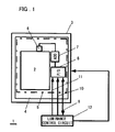
- FIG. 1 is an outline drawing of a display device relating to a first embodiment of the present invention.
- FIG. 2 is a drawing showing the voltage-current characteristics of a photodiode.
- FIG. 3 is an outline drawing of a display device relating to an alternative example of the first embodiment of the present invention.
- FIG. 4 is an outline drawing of a display device relating to a second embodiment of the present invention.
- FIG. 5 is an outline drawing of a display device relating to an alternative example of the second embodiment of the present invention.
- FIG. 6 is an outline drawing of a display device relating to an alternative example of the second embodiment of the present invention.
- FIG. 7 is an outline drawing of a display device relating to a third embodiment of the present invention.
- FIG. 8 is a drawing showing the outline structure of the liquid crystal display device of a mobile phone relating to an embodiment of the present invention.
- FIG. 9 is a block diagram showing the function structure of an LCD described in Patent Document 1.
- FIG. 10 is a drawing showing the structure of an LCD described in Patent Document 4.
- the display device 1 relating to the present embodiment comprises an optical sensor 6 , analog-to-digital converter circuit (ADC hereinafter) 7 , and a serial-parallel converter circuit 8 provided on a substrate 4 on which a TFT driving pixels is provided, converts an output signal of the sensor 6 into a digital signal, and enables the digital signal converted into serial data to be transmitted to use it for the luminance control of the display device, corresponding to external chip-select signals.
- ADC analog-to-digital converter circuit
- FIG. 1 is an outline drawing of the display device relating to the first embodiment of the present invention.
- the display device 1 comprises a backlight 3 , which is the light source, the TFT substrate 4 , on which the pixels (electrodes) and the TFT driving liquid crystal are provided, a counter substrate 5 disposed so that a liquid crystal layer, not shown in the drawing, is interposed between the TFT substrate 4 and the counter substrate 5 , and a luminance control circuit 12 outside of the substrates, and a display region 2 is provided.
- the optical sensor 6 using a photodiode is formed using the means described in Japanese Patent Kokai Publication No. JP-A-06-11690 or the like.
- the ADC 7 that converts an analog signal outputted from the optical sensor 6 into a digital signal, and the parallel-serial converter circuit (P/S hereinafter) 8 that parallel-serial converts the digital data from the ADC 7 into serial data are formed on the TFT substrate 4 .
- the optical sensor 6 is provided near the display region 2 .
- ADC 7 and P/S 8 are constituted to include the TFT formed on the glass substrate that comprises the TFT substrate 4 , and each of them is wired and provided near the optical sensor 6 .
- a serial bus 9 for transmitting the signal from the P/S 8 a transmission path for a chip-select signal (CS hereinafter) 10 that activates the serial bus 9 , and a transmission path for a timing clock (CLK hereinafter) 11 that becomes the reference when the serial bus 9 , activated by the CS 10 , outputs a signal are provided.
- the luminance control circuit 12 can control the current flowing in the backlight 3 , and it controls the luminance of the backlight 3 based on the serial data from the P/S 8 .
- FIG. 2 is a drawing showing the voltage-current characteristics of the photodiode of the optical sensor 6 provided on the TFT substrate 4 .
- FIG. 2 also shows a voltage-current characteristic curve 13 indicating the voltage-current characteristics of the photodiode when the illuminance by external light is low, and a voltage-current characteristic curve 14 indicating the voltage-current characteristics of the photodiode when the illuminance by external light is high.
- V 1 shown in FIG. 2
- V 1 shown in FIG. 2
- a low current value I 1 flows in the optical sensor 6 , provided near the display region 2 .
- This current value I 1 is converted into a digital signal by the ADC 7 , and into serial digital data by the P/S 8 .
- the serial bus 9 connected to the P/S 8 becomes active, and this digital data is transmitted to the luminance control circuit 12 via the serial bus 9 in sync with the CLK 11 .
- the luminance control circuit 12 which has received the digital data, detects that the illuminance of external light is low from the value of the data. In this case, the luminance control circuit 12 controls so that a current corresponding to a low luminance flows in the LED of the backlight 3 since the display can be recognized even with a low backlight luminance.
- a high current I 2 flows in the optical sensor 6 , provided near the display region 2 .
- the current value I 2 is converted into a digital signal by the ADC 7 , and into serial digital data by the P/S 8 .
- the serial bus 9 connected to the P/S 8 becomes active, and this digital data is transmitted to the luminance control circuit 12 via the serial bus 9 in sync with the CLK 11 .
- the luminance control circuit 12 which has received the digital data, detects that the illuminance of external light is high from the value of the data.
- the luminance control circuit 12 controls so that a current corresponding to a high luminance flows in the LED of the backlight 3 , increasing the luminance of the backlight 3 so that the display is easy to see.
- the above-described control is performed continuously while the CS 10 is being supplied to the P/S 8 . Therefore, it becomes possible to automatically increase the luminance in a bright area in order to enhance the visibility of the display or to automatically decrease the luminance in a dark area, according to the variation of the external light illuminance.
- the CS 10 is not supplied, deactivating the serial bus 9 , and the serial bus 9 is detached from the P/S 8 .
- the structure described above enables the small signal flowing in the photodiode to be converted into a digital signal, which has a stronger immunity against noise, by the ADC 7 disposed near the photodiode, and then supplied to the luminance control circuit 12 . Therefore, the influence of the noise entering into the wiring lines connected to the luminance control circuit 12 can be minimized and an accurate luminance control can be performed.
- the method in which the chip-select signal CS 10 is supplied when the P/S 8 converts the data into serial data and outputs externally is employed.
- the microwire interface which has been used already, can be used for controlling the luminance of a mobile phone.
- this structure does not require an external separate circuit, and it can achieve the automatic luminance control without causing increases in size of the device and cost.
- the optical sensor 6 is disposed on the top of the display region, as illustrated in FIG. 1 , however, note that the present invention is not limited to the above example. In terms of the visibility of the display region, the location of the optical sensor is not restricted as long as it is disposed in a location where it can detect the illuminance around the display region.
- the optical sensor 6 is formed as a light-detecting element using a photodiode, and its output current is detected, however, the present invention is not limited to this example, and the similar effects can be achieved by using other devices that change their voltage or current reacting to external light such as phototransistor.
- the present invention is applied to a transmission-type LCD having the light source provided in the back as the display device 1 , however, the present invention is not limited to this example, and can be applied to a reflection-type LCD that has the light source disposed in the front side of the substrate and displays a picture by reflecting the light source or external light or to a display device that uses a self-luminous element such as organic electro-luminescence element.
- the present invention is not limited to this example and it is evident that it can also adjust the luminance in many steps by dividing the signal from the optical sensors into multiple steps to control the luminance.
- the output from the optical sensor 6 is directly received by the ADC 7 , however, the present invention is not limited to this example, and a structure even more resistant to external noise can be achieved by providing an amplifier circuit 37 near the optical sensor 6 as shown in FIG. 3 , and having the amplifier circuit 37 receive the signal before transmitting it to the ADC.
- FIG. 4 is an outline drawing of the display device relating to the second embodiment of the present invention.
- the display device 1 comprises a backlight 3 , a TFT substrate 4 , on which pixels (electrodes) and a TFT driving liquid crystal are provided, and a counter substrate 5 disposed so that a liquid crystal layer, not shown in the drawing, is interposed between the TFT substrate 4 and the counter substrate 5 , and a display region 2 is provided.
- an optical sensor 6 using a photodiode is formed using the means described in Japanese Patent Kokai Publication No. JP-A-06-11690 or the like.
- a luminance control circuit 15 that controls the luminance of the backlight 3 based on a signal from the optical sensor 6 is formed on the top of the TFT substrate 4 .
- the optical sensor 6 is provided near the display region 2 .
- the luminance control circuit 15 is constituted to include the TFT formed on the glass substrate that comprises the TFT substrate 4 , and is wired and provided near the optical sensor 6 .
- a serial bus 16 that transfers external commands and data for controlling the luminance control circuit 15 , a transmission path for a chip-select signal (CS hereinafter) 17 that activates the serial bus 16 , and a transmission path for a timing clock (CLK hereinafter) 18 that becomes the reference when the serial bus 16 , activated by the CS 17 , outputs a signal are provided.
- the luminance control circuit 15 can control the current flowing in the backlight 3 , and it controls the luminance of the backlight 3 based on the output from the optical sensor 6 .
- An analog signal outputted from the optical sensor 6 is supplied to the luminance control circuit 15 on the TFT substrate 4 .
- the luminance control circuit 15 detects the illuminance of external light and performs luminance control of the backlight 3 . Since the optical sensor 6 and luminance control circuit 15 are provided near the top of the TFT substrate, the output signal of the optical sensor 6 can minimize the influence from external noise and perform luminance control.
- Some mobile phones have a function of decreasing the power consumption of the display device by lowering the luminance of the backlight after a certain period of time has passed.
- a mobile phone to which the present invention is applied can achieve this function as well.
- the CS 17 is supplied to the luminance control circuit 15 from an external CPU, activating the serial bus 16 connected to the luminance control circuit 15 .
- command data for lowering the luminance is transmitted to the luminance control circuit 15 via the serial bus 16 in sync with the CLK 18 .
- the luminance control circuit 15 having received the command data, controls so that the current flowing in the LED of the backlight 3 is lowered in order to decrease the power consumption regardless of the brightness of external light.
- the structure of the present embodiment it is possible to decrease the power consumption not only when the illuminance changes by external light, but also when the device is not being used. Needles to say, in the case where the illuminance detection, automatic light control, and the above described off-control of the backlight after a certain period of time has passed are not being performed, the CS 17 is not supplied, deactivating the serial bus 16 , and the serial bus 16 is detached from the luminance control circuit 15 .
- the present invention is not limited to this example, and an amplifier circuit 37 and an ADC 7 can be provided between the optical sensor 6 and the luminance control circuit 15 as shown in FIGS. 5 and 6 , having the amplifier circuit 37 and the ADC 7 receive the signal before transmitting it to the luminance control circuit.
- the above embodiment does not have any restrictions in terms of the location of the optical sensor, the type of the sensor device and the display device, and it can be applied to many display devices that require light control.
- FIG. 7 is an oblique perspective drawing showing the outline structure of the display device relating to the third embodiment of the present invention.
- the display device 1 comprises a backlight 3 , a TFT substrate 4 , on which pixels (electrodes) and a TFT driving liquid crystal are provided, a counter substrate 5 disposed so that a liquid crystal layer, not shown in the drawing, is interposed between the TFT substrate 4 and the counter substrate 5 , and a luminance control circuit 24 , and a display region 2 is provided.
- an optical sensor 6 using a photodiode and a thin film wiring 19 are formed using the means described in Japanese Patent Kokai Publication No. JP-A-06-11690 or the like.
- an IC 20 that includes an ADC and P/S is directly mounted in an area of the TFT substrate that is not covered by the counter substrate 5 .
- the optical sensor 6 is provided near the display region 2 .
- a serial bus 21 for transmitting the signal from the IC 20 a transmission path for a CS 22 that activates the serial bus 21 , and a transmission path for a CLK 23 that becomes the reference when the serial bus 21 , activated by the CS 22 , outputs a signal are provided.
- the luminance control circuit 24 can control the current flowing in the backlight 3 , and it controls the luminance of the backlight 3 based on the serial data from the IC 20 .
- An analog signal outputted by the optical sensor 6 is supplied to the IC 20 via the wiring 19 , and converted into serial digital data by the ADC and P/S.
- the serial bus 21 becomes active and the IC 20 transmits the data to the luminance control circuit 24 via the serial bus 21 in sync with the CLK 23 .
- the luminance control circuit 24 having received the digital data, can automatically adjust the luminance of the display device by controlling the luminance of the backlight 3 based on the value of the data.
- This luminance control can be performed without much influence from external noise since the wiring 19 only connects a short distance within the TFT substrate 4 . Further, because the signal communication with the outside of the display device can be performed with a small number of wiring lines, the size of the device can be made smaller.
- the present invention is not limited to this example, and it is evident that the same effects can be achieved by employing a structure where an IC including only parts of the ADC and P/S circuits is used and the rest of the circuits is constituted by the TFT formed on the TFT substrate.
- the luminance control of a display device according to the external light illuminance can be performed by the display device independently without communicating with the outside. It is because a sensor and current control circuit (luminance control circuit 24 ) for the illumination of the display device are provided on the side of the display device.
- FIG. 8 is drawing showing a circuit structure relating to the luminance control of the backlight of the LCD of a mobile phone relating to an embodiment of the present invention.
- a main LCD 28 a main LCD 28 , sub-display (not shown in the drawing), camera (not shown in the drawing), an application processor 25 that controls other devices, a power supply IC 26 that supplies the power to each of the function blocks, battery 27 that supplies the power to the power supply IC 26 , main LCD 28 , the LCD section (display region) 29 of the main LCD 28 , a TFT substrate 30 that constitutes the main LCD 28 , and backlight 36 for the main LCD are shown.
- an optical sensor 31 using a photodiode, an amplifier circuit 32 , ADC 33 , and a P/S 34 are formed using the means described in Japanese Patent Kokai Publication No. JP-A-06-11690 or the like.
- the optical sensor 31 is provided near the LCD section (display region) 29 .
- the amplifier circuit 32 , ADC 33 and P/S 34 are constituted to include the TFT formed on the glass substrate that comprises the TFT substrate 30 , and each of them is wired and provided near the LCD section (display region) 29 .
- the application processor 25 can read a luminance map that stores the information, expressed as digital data, on the relationship between external light illuminance and the target luminance of the backlight. Also, the application processor 25 is connected by a microwire interface 35 that controls the operation of the power supply IC 26 and P/S. More concretely, the microwire interface 35 comprises four lines: two bus lines for transferring the serial data, a chip-select line that selects a device (a CS 1 selects the P/S 34 and a CS 2 selects the power supply IC 26 ), and a clock that transmits a timing signal for transferring data with the device selected by the chip-select line.
- the application processor 25 selects the CS 1 activating the output of the P/S 34 . Then, the application processor 25 receives the digital data supplied from the P/S 34 via the serial bus line (the double-arrowed line) in sync with the clock signal CLK supplied to the P/S 34 .
- the data outputted from the P/S 34 at this time is obtained as follows: a current that flows in the optical sensor 31 when it receives external light is converted into a voltage with the amplifier circuit 32 , then, analog-to-digital converted by the ADC 33 , and parallel-serial converted by the P/S 34 .
- the application processor 25 refers to the luminance map and calculates the target luminance of the backlight that corresponds to the digital data inputted. Meanwhile, the serial bus line (the double-arrowed line) of the power supply IC 26 is not active since the CS 2 is not selected, and the power supply IC 26 is not influenced by the serial bus line.
- the application processor 25 will not change the luminance of the backlight 36 and it will move to another operation.
- the application processor will move to the following operation.
- the application processor 25 selects the CS 2 of the microwire interface 35 and activates the serial bus line of the power supply IC 26 . Then, the application processor 25 transmits a command for setting the backlight 36 to the luminance that corresponds to the map to the power supply IC 26 via the serial bus line in sync with the clock signal CLK.
- the power supply IC 26 having received the above-mentioned command, stores the data that corresponds to this backlight luminance, and changes the current value supplied to the backlight 36 based on this data.
- the serial bus line (the double-arrowed line) is inactive since the CS 1 is not selected, and the P/S 34 is not influenced by the serial bus line.
Abstract
Description
- [Patent Document 1]
- [Patent Document 2]
- [Patent Document 3]
- [Patent Document 4]
- [Patent Document 5]
- [Patent Document 6]
Claims (20)
Applications Claiming Priority (2)
| Application Number | Priority Date | Filing Date | Title |
|---|---|---|---|
| JP2004-206212 | 2004-07-13 | ||
| JP2004206212A JP2006030392A (en) | 2004-07-13 | 2004-07-13 | Display device and electronic equipment using the same |
Publications (2)
| Publication Number | Publication Date |
|---|---|
| US20060012543A1 US20060012543A1 (en) | 2006-01-19 |
| US8072444B2 true US8072444B2 (en) | 2011-12-06 |
Family
ID=35598918
Family Applications (1)
| Application Number | Title | Priority Date | Filing Date |
|---|---|---|---|
| US11/180,103 Active 2029-11-13 US8072444B2 (en) | 2004-07-13 | 2005-07-13 | Display device and electronic apparatus using the same |
Country Status (3)
| Country | Link |
|---|---|
| US (1) | US8072444B2 (en) |
| JP (1) | JP2006030392A (en) |
| CN (1) | CN1721929B (en) |
Cited By (6)
| Publication number | Priority date | Publication date | Assignee | Title |
|---|---|---|---|---|
| US20080055231A1 (en) * | 2006-08-30 | 2008-03-06 | Nec Electronics Corporation | Mobile terminal and display panel driver |
| US20090167675A1 (en) * | 2007-12-27 | 2009-07-02 | Park Jaedeok | Liquid crystal display and driving method thereof |
| US20090230882A1 (en) * | 2008-03-11 | 2009-09-17 | Hendrik Santo | Architecture and technique for inter-chip communication |
| US20090231247A1 (en) * | 2008-03-11 | 2009-09-17 | Tushar Dhayagude | Methods and circuits for self-calibrating controller |
| US20090315467A1 (en) * | 2008-06-24 | 2009-12-24 | Msilica Inc | Apparatus and methodology for enhancing efficiency of a power distribution system having power factor correction capability by using a self-calibrating controller |
| US20100237786A1 (en) * | 2009-03-23 | 2010-09-23 | Msilica Inc | Method and apparatus for an intelligent light emitting diode driver having power factor correction capability |
Families Citing this family (10)
| Publication number | Priority date | Publication date | Assignee | Title |
|---|---|---|---|---|
| US20090051678A1 (en) * | 2005-06-15 | 2009-02-26 | Masakazu Satoh | Active Matrix Display Apparatus |
| KR20070024235A (en) * | 2005-08-26 | 2007-03-02 | 삼성전자주식회사 | Backlight unit, display device having the same and driving method of the same |
| US20090015540A1 (en) * | 2006-01-20 | 2009-01-15 | Nec Corporation | Portable terminal |
| JP2008268642A (en) * | 2007-04-23 | 2008-11-06 | Sony Corp | Backlight device, method for controlling backlight and liquid crystal display device |
| JP2010175997A (en) * | 2009-01-30 | 2010-08-12 | Toshiba Corp | Electronic apparatus |
| CN106057137A (en) * | 2016-08-22 | 2016-10-26 | 信利光电股份有限公司 | Display device and brightness control method thereof |
| CN106297679B (en) * | 2016-09-19 | 2017-09-15 | 京东方科技集团股份有限公司 | Display device and the method for controlling display device brightness |
| CN108040360B (en) | 2017-12-05 | 2020-12-11 | 北京小米移动软件有限公司 | Method and device for controlling screen display |
| KR102618734B1 (en) * | 2018-11-19 | 2023-12-29 | 삼성디스플레이 주식회사 | Display device and method of driving the same |
| CN109683384B (en) * | 2019-02-15 | 2021-12-07 | 合肥鑫晟光电科技有限公司 | Display panel and display device |
Citations (15)
| Publication number | Priority date | Publication date | Assignee | Title |
|---|---|---|---|---|
| JPS61259287A (en) | 1985-05-14 | 1986-11-17 | 三菱電機株式会社 | Liquid crystal display unit |
| JPS646927A (en) | 1987-06-29 | 1989-01-11 | Hosiden Electronics Co | Liquid crystal display device |
| JPH02309316A (en) | 1989-05-25 | 1990-12-25 | Nec Corp | Liquid crystal display device |
| JPH03249622A (en) | 1990-02-28 | 1991-11-07 | Toshiba Corp | Liquid crystal display device |
| JPH04352128A (en) | 1991-05-30 | 1992-12-07 | Mitsubishi Electric Corp | Liquid crystal display device |
| JPH0611690A (en) | 1992-06-26 | 1994-01-21 | Rohm Co Ltd | Liquid crystal display device |
| JPH06332385A (en) | 1993-05-18 | 1994-12-02 | Sharp Corp | Display device |
| JP2000122575A (en) | 1998-10-20 | 2000-04-28 | Casio Comput Co Ltd | Display device |
| CN1327223A (en) | 2000-06-06 | 2001-12-19 | 索尼公司 | Modulation circuit and image display using said modulation circuit |
| JP2002175026A (en) | 2000-12-07 | 2002-06-21 | Sony Corp | Active matrix type display device and portable terminal using the same |
| US20040012556A1 (en) | 2002-07-17 | 2004-01-22 | Sea-Weng Yong | Method and related device for controlling illumination of a backlight of a liquid crystal display |
| US6717560B2 (en) * | 2000-05-15 | 2004-04-06 | Eastman Kodak Company | Self-illuminating imaging device |
| US6961038B2 (en) * | 2000-11-30 | 2005-11-01 | Canon Kabushiki Kaisha | Color liquid crystal display device |
| US20060007097A1 (en) | 2003-12-08 | 2006-01-12 | Sony Corporation | Liquid crystal display and backlight adjusting method |
| US7592980B2 (en) * | 2002-06-05 | 2009-09-22 | Semiconductor Energy Laboratory Co., Ltd. | Semiconductor device |
-
2004
- 2004-07-13 JP JP2004206212A patent/JP2006030392A/en active Pending
-
2005
- 2005-07-11 CN CN200510083553.9A patent/CN1721929B/en active Active
- 2005-07-13 US US11/180,103 patent/US8072444B2/en active Active
Patent Citations (17)
| Publication number | Priority date | Publication date | Assignee | Title |
|---|---|---|---|---|
| JPS61259287A (en) | 1985-05-14 | 1986-11-17 | 三菱電機株式会社 | Liquid crystal display unit |
| JPS646927A (en) | 1987-06-29 | 1989-01-11 | Hosiden Electronics Co | Liquid crystal display device |
| JPH02309316A (en) | 1989-05-25 | 1990-12-25 | Nec Corp | Liquid crystal display device |
| JPH03249622A (en) | 1990-02-28 | 1991-11-07 | Toshiba Corp | Liquid crystal display device |
| JPH04352128A (en) | 1991-05-30 | 1992-12-07 | Mitsubishi Electric Corp | Liquid crystal display device |
| JPH0611690A (en) | 1992-06-26 | 1994-01-21 | Rohm Co Ltd | Liquid crystal display device |
| JPH06332385A (en) | 1993-05-18 | 1994-12-02 | Sharp Corp | Display device |
| JP2000122575A (en) | 1998-10-20 | 2000-04-28 | Casio Comput Co Ltd | Display device |
| US6717560B2 (en) * | 2000-05-15 | 2004-04-06 | Eastman Kodak Company | Self-illuminating imaging device |
| US20020017962A1 (en) | 2000-06-06 | 2002-02-14 | Yuichi Takagi | Modulation circuit and image display using the same |
| CN1327223A (en) | 2000-06-06 | 2001-12-19 | 索尼公司 | Modulation circuit and image display using said modulation circuit |
| US6961038B2 (en) * | 2000-11-30 | 2005-11-01 | Canon Kabushiki Kaisha | Color liquid crystal display device |
| JP2002175026A (en) | 2000-12-07 | 2002-06-21 | Sony Corp | Active matrix type display device and portable terminal using the same |
| US7592980B2 (en) * | 2002-06-05 | 2009-09-22 | Semiconductor Energy Laboratory Co., Ltd. | Semiconductor device |
| US20040012556A1 (en) | 2002-07-17 | 2004-01-22 | Sea-Weng Yong | Method and related device for controlling illumination of a backlight of a liquid crystal display |
| US20060007097A1 (en) | 2003-12-08 | 2006-01-12 | Sony Corporation | Liquid crystal display and backlight adjusting method |
| CN1774665A (en) | 2003-12-08 | 2006-05-17 | 索尼株式会社 | Liquid crystal display and backlight adjusting method |
Non-Patent Citations (1)
| Title |
|---|
| JP Official Action dated Jan. 26, 2010 together with partial translation. |
Cited By (11)
| Publication number | Priority date | Publication date | Assignee | Title |
|---|---|---|---|---|
| US20080055231A1 (en) * | 2006-08-30 | 2008-03-06 | Nec Electronics Corporation | Mobile terminal and display panel driver |
| US20090167675A1 (en) * | 2007-12-27 | 2009-07-02 | Park Jaedeok | Liquid crystal display and driving method thereof |
| US8847875B2 (en) * | 2007-12-27 | 2014-09-30 | Lg Display Co., Ltd. | Liquid crystal display and driving method thereof |
| US20090230882A1 (en) * | 2008-03-11 | 2009-09-17 | Hendrik Santo | Architecture and technique for inter-chip communication |
| US20090231247A1 (en) * | 2008-03-11 | 2009-09-17 | Tushar Dhayagude | Methods and circuits for self-calibrating controller |
| US8493300B2 (en) * | 2008-03-11 | 2013-07-23 | Atmel Corporation | Architecture and technique for inter-chip communication |
| US8581810B2 (en) | 2008-03-11 | 2013-11-12 | Atmel Corporation | Methods and circuits for self-calibrating controller |
| US20090315467A1 (en) * | 2008-06-24 | 2009-12-24 | Msilica Inc | Apparatus and methodology for enhancing efficiency of a power distribution system having power factor correction capability by using a self-calibrating controller |
| US8314572B2 (en) | 2008-06-24 | 2012-11-20 | Atmel Corporation | Apparatus and methodology for enhancing efficiency of a power distribution system having power factor correction capability by using a self-calibrating controller |
| US20100237786A1 (en) * | 2009-03-23 | 2010-09-23 | Msilica Inc | Method and apparatus for an intelligent light emitting diode driver having power factor correction capability |
| US8441199B2 (en) | 2009-03-23 | 2013-05-14 | Atmel Corporation | Method and apparatus for an intelligent light emitting diode driver having power factor correction capability |
Also Published As
| Publication number | Publication date |
|---|---|
| CN1721929B (en) | 2010-11-03 |
| JP2006030392A (en) | 2006-02-02 |
| US20060012543A1 (en) | 2006-01-19 |
| CN1721929A (en) | 2006-01-18 |
Similar Documents
| Publication | Publication Date | Title |
|---|---|---|
| US8072444B2 (en) | Display device and electronic apparatus using the same | |
| KR101330817B1 (en) | Liquid crystal display device and driving thereof | |
| KR101229019B1 (en) | Liquid crystal display device and driving circuit of the same | |
| US8194031B2 (en) | Backlight control of electronic device | |
| US8669933B2 (en) | Liquid crystal display, electronic device, and method for controlling brightness of illumination unit of liquid crystal display | |
| KR101284926B1 (en) | Liquid Crystal Display Device And fabricating Method and Driving Method Thereof | |
| US8830157B2 (en) | Display apparatus, quantity-of-light adjusting method for display apparatus and electronic equipment | |
| CN101675466B (en) | Display device, display control method and electronic device | |
| US8842242B2 (en) | Liquid crystal display, estimating method of ambient light and driving method of liquid crystal display | |
| US7889158B2 (en) | Electrooptic device and electronic device | |
| WO2003050602A1 (en) | Reflection liquid crystal display apparatus | |
| JP4667079B2 (en) | Display device | |
| MX2009001822A (en) | Multiple light sensors and algorithms for luminance control of mobile display devices. | |
| KR101457683B1 (en) | Liquid Crystal Display | |
| US20110001728A1 (en) | Pointing device and display device using the same | |
| KR20110071388A (en) | Liquid crystal display device and method for controlling automatic brightness | |
| KR20240003745A (en) | Drive circuit, display module and display device | |
| CN102314247B (en) | Touch panel | |
| KR101325977B1 (en) | Photo sensor build-in LCD | |
| US20070200817A1 (en) | Driving device with light sensor module and electronic device using the same | |
| JP2008064828A (en) | Liquid crystal device and electronic apparatus | |
| US9697797B2 (en) | Method and apparatus for displaying content | |
| KR20080037187A (en) | Liquid crystal display | |
| KR20070060469A (en) | Liquid crystal display device and driving method | |
| CN201765801U (en) | Plane display device capable of automatically adjusting brightness |
Legal Events
| Date | Code | Title | Description |
|---|---|---|---|
| AS | Assignment |
Owner name: NEC CORPORATION, JAPAN Free format text: ASSIGNMENT OF ASSIGNORS INTEREST;ASSIGNORS:IKEDA, NAOYASU;HAGA, HIROSHI;OTOSE, TOMOHIKO;AND OTHERS;REEL/FRAME:016749/0420 Effective date: 20050707 |
|
| STCF | Information on status: patent grant |
Free format text: PATENTED CASE |
|
| AS | Assignment |
Owner name: GOLD CHARM LIMITED, SAMOA Free format text: ASSIGNMENT OF ASSIGNORS INTEREST;ASSIGNOR:NEC CORPORATION;REEL/FRAME:030024/0604 Effective date: 20121130 |
|
| FPAY | Fee payment |
Year of fee payment: 4 |
|
| MAFP | Maintenance fee payment |
Free format text: PAYMENT OF MAINTENANCE FEE, 8TH YEAR, LARGE ENTITY (ORIGINAL EVENT CODE: M1552); ENTITY STATUS OF PATENT OWNER: LARGE ENTITY Year of fee payment: 8 |
|
| AS | Assignment |
Owner name: HANNSTAR DISPLAY CORPORATION, TAIWAN Free format text: ASSIGNMENT OF ASSIGNORS INTEREST;ASSIGNOR:GOLD CHARM LIMITED;REEL/FRAME:063351/0517 Effective date: 20230320 |
|
| MAFP | Maintenance fee payment |
Free format text: PAYMENT OF MAINTENANCE FEE, 12TH YEAR, LARGE ENTITY (ORIGINAL EVENT CODE: M1553); ENTITY STATUS OF PATENT OWNER: LARGE ENTITY Year of fee payment: 12 |