US8072463B1 - Graphics system with virtual memory pages and non-power of two number of memory elements - Google Patents

Graphics system with virtual memory pages and non-power of two number of memory elements Download PDF

Info

Publication number
US8072463B1
US8072463B1 US11/538,755 US53875506A US8072463B1 US 8072463 B1 US8072463 B1 US 8072463B1 US 53875506 A US53875506 A US 53875506A US 8072463 B1 US8072463 B1 US 8072463B1
Authority
US
United States
Prior art keywords
partition
partitions
memory
graphics
graphics system
Prior art date
Legal status (The legal status is an assumption and is not a legal conclusion. Google has not performed a legal analysis and makes no representation as to the accuracy of the status listed.)
Active, expires
Application number
US11/538,755
Inventor
James M. Van Dyke
John H. Edmondson
John S. Montrym
Current Assignee (The listed assignees may be inaccurate. Google has not performed a legal analysis and makes no representation or warranty as to the accuracy of the list.)
Nvidia Corp
Original Assignee
Nvidia Corp
Priority date (The priority date is an assumption and is not a legal conclusion. Google has not performed a legal analysis and makes no representation as to the accuracy of the date listed.)
Filing date
Publication date
Application filed by Nvidia Corp filed Critical Nvidia Corp
Priority to US11/538,755 priority Critical patent/US8072463B1/en
Assigned to NVIDIA CORPORATION reassignment NVIDIA CORPORATION ASSIGNMENT OF ASSIGNORS INTEREST (SEE DOCUMENT FOR DETAILS). Assignors: EDMONDSON, JOHN H., MONTRYM, JOHN S., VAN DYKE, JAMES M.
Application granted granted Critical
Publication of US8072463B1 publication Critical patent/US8072463B1/en
Active legal-status Critical Current
Adjusted expiration legal-status Critical

Links

Images

Classifications

    • GPHYSICS
    • G06COMPUTING; CALCULATING OR COUNTING
    • G06FELECTRIC DIGITAL DATA PROCESSING
    • G06F12/00Accessing, addressing or allocating within memory systems or architectures
    • G06F12/02Addressing or allocation; Relocation
    • G06F12/06Addressing a physical block of locations, e.g. base addressing, module addressing, memory dedication
    • G06F12/0607Interleaved addressing
    • GPHYSICS
    • G06COMPUTING; CALCULATING OR COUNTING
    • G06FELECTRIC DIGITAL DATA PROCESSING
    • G06F12/00Accessing, addressing or allocating within memory systems or architectures
    • G06F12/02Addressing or allocation; Relocation
    • G06F12/08Addressing or allocation; Relocation in hierarchically structured memory systems, e.g. virtual memory systems
    • G06F12/10Address translation

Definitions

  • the present invention is generally related to partitioned memories. More particularly, the present invention is directed towards partitioned graphics memories.
  • a partitioned graphics memory has a number of partitions that are each operative to independently service memory requests from a plurality of memory clients while maintaining the appearance to a na ⁇ ve memory client of a unitary memory system.
  • a partitioned graphics memory provides several advantages.
  • One advantage is that since conventional dynamic random access memories (DRAMs) come in a limited number of standard sizes, a partitioned graphics memory allows an increase in the effective memory size, which improves performance.
  • DRAMs dynamic random access memories
  • FIG. 1 illustrates a memory system 100 similar to that described in U.S. patent Ser. No. 10/740,229 by Van Dyke et al., the contents of which are hereby incorporated by reference.
  • a memory system 100 for a partitioned memory system 100 includes two or more memory partitions, with the total number of partitions being equal to a power of two, such as four partitions.
  • Each partition P0 115 , P1 120 , P2 125 , and P3 130 is coupled to a memory controller 105 by its own respective data bus 135 .
  • Each data bus 135 has a memory byte width, W p , with an associated packet width for addressing locations within the partition.
  • W p memory byte width
  • a packet is a unit of data transfer.
  • each partition may have sub-partitions, such as two sub-partitions SP 0 140 A and SP 1 140 B.
  • Each sub-partition 140 A and 140 B has its own respective sub-bus 148 with a corresponding byte width for sub-packets, W sp , addressed to a memory location in the sub-partition.
  • W sp sub-packets
  • the sub-partitions are thus the minimum addressable unit of the graphics system.
  • Each sub-partition may, for example, be a double data rate (DDR) dynamic random access memory (DRAM).
  • DDR double data rate
  • DRAM dynamic random access memory
  • each partition may have 64 data pins whereas each sub-partition 140 A or 140 B has 32 data pins. This permits, for example, a 64 bit partition to be implemented as two conventional 32 bit memory chips.
  • the memory controller 105 routes addresses of requests from individual clients of a graphics system to specific partition/sub-partition memory locations.
  • the individual clients may be any component within a graphics processing system that requires access to a graphics memory to read, write, clear, or compress tile data.
  • An arbitration module 150 selects a client 155 or 160 .
  • a partition address routing module 190 maps an address associated with a client (e.g., a read or write request) to a memory location in a partition and its associated sub-partitions.
  • a compression/decompression module 165 is included to compress and decompress tile data to reduce memory bandwidth requirements.
  • a tag module 170 may be included to identify, by a tag (e.g., one or more bits) attributes of the tiles, such as whether a tile holds data in a compressed format.
  • a packing/unpacking state machine 180 and format conversion module 195 are provided to reorganize tile data.
  • partitioning permits the total effective number of DRAM data pins to be increased compared to an individual DRAM.
  • the total effective number of data pins for the partitioned graphics memory is the number of data pins per partition multiplied by the number of partitions.
  • the equivalent DRAM memory size of partitioned graphics memories have increased from 128 pins (2 7 ) to 256 pins (2 8 ) in current generation products.
  • the number of DRAMs in a partitioned graphics memory is a power of two.
  • binary address spaces naturally scale as a power of two.
  • many other attributes of a computer system also typically scale as a power of two.
  • conventional partitioned graphics memories utilize a power of two number of partitions (e.g., four) and have a power of two number of DRAMs (e.g., eight DRAMs in a partitioned graphics memory having four partitions and two DRAMs per partition).
  • a graphics system utilizes virtual memory pages and has a partitioned graphics memory that includes memory elements.
  • the partitioned graphics memory supports a non-power of two number of operative memory elements.
  • the memory elements are dynamic random access memories (DRAMs) and the graphics system supports having a total number of active DRAMs that is not equal to a power of two.
  • DRAMs dynamic random access memories
  • a partition swizzling operation is used to adjust the partition numbers associated with individual units of virtual memory allocation on particular virtual memory pages to achieve a selected partition interleaving pattern.
  • One embodiment of a graphics system includes a partitioned graphics memory having a plurality of partitions each including at least one dynamic random access memory (DRAM).
  • the graphics system includes a graphics processing unit coupled to the partitioned graphics memory.
  • An address translation module in the graphics processing unit performs an address translation to map virtual addresses to physical addresses and determines individual partitions associated with memory accesses for individual units of virtual memory allocation.
  • the graphics system performs partition interleaving in which data for an individual unit of virtual memory allocation is assigned to one partition and different individual units of virtual memory allocation are assigned to different partitions.
  • the graphics system performs a partition swizzling operation to adjust the partition numbers associated with the individual units of virtual memory allocation on particular virtual memory pages to achieve a selected partition interleaving pattern.
  • FIG. 1 is a block diagram of a prior art partitioned graphics memory
  • FIG. 2 is a block diagram of a graphics system with a partitioned graphics memory having a non power of two number of partitions according to one embodiment of the present invention
  • FIG. 3 is a block diagram of a graphics system with a partitioned graphics memory having a non-power of two number of DRAMs per partition according to one embodiment of the present invention
  • FIG. 4 illustrates a memory management unit (MMU) process for determining partition number and DRAM row-column-bank addresses according to one embodiment of the present invention
  • FIG. 5 illustrates an exemplary sequence of address translations according to one embodiment of the present invention
  • FIG. 6 illustrates an exemplary gob of a block-linear memory format in accordance with one embodiment of the present invention
  • FIG. 7 illustrates an exemplary block of a block-linear memory format in accordance with one embodiment of the present invention
  • FIG. 8 illustrates an exemplary row of a block-linear memory format in accordance with one embodiment of the present invention
  • FIG. 9 illustrates a mapping of a surface in a block-liner memory format in accordance with one embodiment of the present invention.
  • FIG. 10 illustrates an exemplary gob in accordance with one embodiment of a block-linear memory format
  • FIG. 11 illustrates an exemplary gob partition assignment without swizzling in accordance with one embodiment of the present invention
  • FIG. 12 illustrates an exemplary gob partition assignment with swizzling in accordance with one embodiment of the present invention.
  • FIG. 13 illustrates an exemplary mapping of physical addresses to partition numbers and row-column-bank addresses.
  • FIG. 2 illustrates a graphics system 200 in accordance with one embodiment of the present invention.
  • a graphics processing unit 205 includes a memory controller 210 to interface a partitioned graphics memory 250 having memory partitions 255 coupled by respective buses 257 to memory controller 210 .
  • Each partition 255 may for example, further include sub-partitions 253 coupled to sub-buses 251 via respective parallel interfaces.
  • Each sub-partition 253 includes a memory element.
  • each sub-partition 253 may include a memory element that is a dynamic random access memory (DRAM).
  • DRAM dynamic random access memory
  • Each DRAM of a sub-partition 253 has parallel interfaces with respect to the other sub-partitions 253 of the same partition 255 such that the total equivalent number of DRAM data pins of each partition 255 scales with the number of sub-partitions 253 .
  • a single partition 255 having two sub-partitions 253 each of which are 32 bit DRAMs results in an equivalent 64 bit access word.
  • Memory controller 210 is capable of interfacing a partitioned memory with a non-power of two number of DRAMs (i.e., the number of operative DRAM memory elements does not equal 2 m , where m is an integer).
  • FIG. 2 illustrates an embodiment with a non-power of two number of partitions (e.g., three partitions with two sub-partitions in each partition) such that the total number of DRAMs is not a power of two.
  • each partition includes a non-power of two number of sub-partitions 253 (e.g., three DRAMs) such that the total number of DRAMs is not equal to a power of two.
  • memory controller 210 is programmable such that it is capable of supporting different numbers of DRAMs, including both a power of two number of DRAMs and a non-power of two number of DRAMs.
  • memory controller 210 may be designed to support different numbers of partitions (e.g., 1, 2, 3, 4, 5, 6, 7, or 8 partitions) and during assembly programmed to support a particular number of partitions.
  • a non-volatile memory may be written to indicate the number of partitions.
  • the number of partitions may be selected, for example, based on cost constraints or yield considerations. For example, the number of partitions selected as operative (active) partitions may be reduced from a maximum number to account for a manufacturing defect.
  • a non-power of two number of partitions may be used is the case where a chip is nominally designed for four partitions but after manufacture has one defective partition.
  • the defective partition can be disabled and a product with three (a non power-of-two) active partitions shipped.
  • the number of partitions may be selected for different market segments.
  • the number of sub-partitions per partition may be based on cost or yield considerations.
  • Memory controller 210 includes an address translation module 215 -A to map memory addresses to particular partitions and row-bank-column addresses within partitions. Memory controller 210 performs address translation on behalf of na ⁇ ve memory clients 230 that lack an address translation capability. However, it will be understood that a sophisticated memory client 235 may include an address translation module 215 -B that performs some or all of the address translation for the sophisticated client.
  • graphics system 200 includes a CPU 260 utilizing virtual memory addressing implemented using virtual memory pages 280 , paging, page tables, and page table entries (PTEs).
  • a system memory 265 stores a graphics application 270 , driver 275 , and a page table 280 .
  • Virtual memory pages 280 are used for memory management and may, for example, be generated to store data for a graphics surface drawn by graphics application 270 .
  • a virtual memory page corresponds to a range of consecutive addresses in a virtual address space, such as a 4 KB page size or a 64 KB page size.
  • Address translation information to map virtual to physical page numbers are stored in page tables associated with individual pages. Individual items in a page table are known as page table entries (PTEs).
  • memory management unit (MMU) logic is used to handle memory access requests and perform address translation from virtual addresses to physical addresses.
  • the virtual address space is divided into pages. Copies of the MMU logic may reside in different locations within the graphics system, depending on the implementation. As illustrated in FIGS. 2 and 3 , a copy of the MMU logic may be included in address translation module 215 -A.
  • a translation lookaside buffer (TLB) 290 in GPU 205 may be used to cache address translation information to translate virtual page numbers to physical page numbers. Page table entries stored in page tables provide additional information for translating addresses. In particular, in a partitioned graphics memory using DRAMs as the memory elements the physical addresses further need to be translated into partition numbers and the row-column-bank addresses within individual DRAMs.
  • FIG. 4 illustrates an exemplary MMU process.
  • the MMU maps input graphics coordinates, such as texture (u,v) coordinates or (x,y) surface coordinates to virtual addresses.
  • a virtual memory page can be considered to be a virtual tile, where a virtual tile describes a region of virtual memory with common properties that maps to a contiguous region of physical memory.
  • the virtual address space is divided into virtual tiles which can be either a power of two in size (e.g., 64 KB) or a graphics non-power of two size, depending on the number of DRAMs.
  • the MMU maps the virtual tile address to the location of the virtual tile in physical memory using page table entries.
  • a virtual address is computed by applying a mapping (such as a pitch or block-linear mapping) onto the coordinates of the surface mapped.
  • a virtual address is determined based, for example, on a virtual offset.
  • a TLB receives PTE information from virtual memory pages.
  • the MMU maps the virtual tile address bits from the virtual address to the location of the virtual tile in physical memory using the PTEs.
  • the PTEs provide information on the “Kind” of data that is stored, and may include information on the data storage formats. Additionally, in one embodiment the PTEs provide information used to generate a partition number and a row-bank-column (RBC) address, such as partition stride, partition swizzle, partition offset or bank swizzle.
  • RBC row-bank-column
  • the low order bits of the virtual address may be used as low order bits of the physical address.
  • High order bits of the virtual address may be used as keys into address translation tables to determine the higher order bits of the physical address.
  • the MMU maps the virtual tile address bits from the virtual address to the location of the virtual tile in memory using the PTEs. The remainder of the bits from the virtual address are then combined with the address of the virtual tile in physical memory to compute the physical address associated with the virtual address requested.
  • bits [7,0] specify the byte within a 256 B physical region
  • bits [15:8] specify a 256 B physical region within the 64 KB virtual tile
  • bits [39:16] specify the virtual tile address.
  • the MMU logic utilizes one or more modulo operations to perform a partition assignment.
  • a modulo operation is an operation in which for two integers a and n, the operation a modulo n, the result is the remainder after division of a by n.
  • the modulo operation is often represented by the “%” character.
  • a modulo operation may be used to “cycle” physical memory addresses assigned to a partition number or a sub-partition number. That is, one or more modulo operations may be performed on appropriately scaled sets of physical memory addresses to assign chunks of physical memory address to partitions or sub-partitions in a cyclic order.
  • a partition number can be assigned using a modulo operation in which the partition number is based on a subset of physical address of the virtual memory page modulo the number of partitions with appropriate scaling, as described below in more detail.
  • a row-column-bank address is determined by taking a select set of physical address bits divided by the number of partitions.
  • FIG. 5 illustrates in more detail an exemplary sequence of address translation operations.
  • a region of a graphics surface is generated by a drawing engine 505 and has (x, y, z) coordinates (for the case that graphics surface region is a two dimensional surface, it has (x, y) coordinates).
  • a first address translation 510 is performed to map the graphics surface region to a one-dimensional virtual address (VA) space.
  • VA virtual address
  • the first address translation may comprise a conventional pitch memory format.
  • first address translation 510 may alternatively comprise a block-linear format to generate virtual addresses, which is described below in more detail.
  • a second address translation 520 is performed to translate the virtual address to a physical address (PA).
  • PA physical address
  • a third address translation 530 generates a raw address from the physical address.
  • the raw address includes the collection of fields needed to uniquely locate each byte in the DRAMs.
  • the raw address includes a partition number (and also sub-partition number, if a sub-partition is included) and a row-bank-column (RBC addresses) within a particular DRAM.
  • the third translation 530 to determine the raw address may, for example, utilize information in a page table entry specifying a data “kind” describing one or more formats for packing tile data (e.g., intra-tile packing).
  • a PTE may comprise fields indicating a compression mode, a multi-sample format, and one or more tile data formats.
  • a PTE may also include fields to support utilization of non-power of two numbers of DRAMs, such as a partition stride field to indicate units of contiguous memory stored within each partition, a partition offset field to adjust the partition number for the start of a page, and a bank swizzle field to perform bank swizzling for non-power of two numbers of DRAMs. It will also be understood that it is contemplated that more generally PTE fields may be provided to provide other types of information useful for performing address translation to optimize the use of a partitioned memory having a non-power of two number of DRAMs.
  • a graphics surface is mapped according to a hierarchical sequence of nested loops of gobs (sub-blocks), blocks, rows of blocks, and a whole surface to perform the mapping between spatial coordinates to virtual addresses.
  • the gob is a selected number of lines tall (e.g., 4 or 8, depending on the implementation) and has a selected byte width (e.g., 64 B)
  • a gob also preferably corresponds to an integer number of DRAM atoms for accessing an individual DRAM.
  • a packing choice may be specified by a page kind field in a page table entry. As illustrated in FIG.
  • a gob corresponds to a rectangular region of memory, such as 256 bytes in virtual address space, which is a minimum unit of allocation of a block-linear surface in virtual address space.
  • An individual gob may also correspond in size to that of a tile or small number of tiles. If a pixel requires 4 B of storage, a 256 B gob represents a 16 by 4 pixel region of a 2D surface.
  • a gob is preferably 256 bytes aligned to 256B such that a gob never crosses a MMU page boundary. As illustrated in FIG. 7 , a set of gobs are organized into a block.
  • a gob typically corresponds to one or more tiles and may be implemented with different numbers of lines.
  • FIG. 10 illustrates a 64B ⁇ 8 line Gob corresponding to two tiles. Individual sub-sections of a Gob may be assigned to different sub-partitions A or B.
  • the block-linear memory format maps graphics surfaces in a way that preserves attributes of the source data and which facilitates efficient access of data.
  • the block attributes may be selected to facilitate utilizing a non-power number of two DRAMs.
  • virtual memory pages may be a power of two size or a non power of two size.
  • the block height is always a power of two (e.g., 2 0 , 2 1 , 2 2 , 2 4 ) number of gobs but the block width can be an integer number of gobs (e.g., 1, 2 or 3).
  • the virtual memory page width varies with the number of partitions.
  • PTE fields may be included to provide information for a MMU to determine a partition number.
  • a PTE is a partition stride.
  • the partition stride is a unit of contiguous virtual/physical memory contained within an individual partition.
  • the partition stride determines how frequently the partition number is stepped as gobs are traversed.
  • the partition stride may correspond to one gob (256B) or a small number of gobs (e.g., four gobs or 1024B).
  • gob-sized regions of contiguous virtual/physical memory addresses are mapped to individual partitions.
  • a consequence of the partition stride is that gobs are interleaved amongst the partitions based, in part, on the partition stride.
  • a PTE may be included for a partition offset.
  • the partition offset is a pre-computed partition number for the location at the start of the page in physical memory.
  • the partition offset determines a starting partition for determining a partition number.
  • MMU logic may use PTE information to determine a partition number based on a modulo operation. For example, with 1024B partitions an exemplary formula for mapping a physical address to a partition number (e.g., Partition [2:0], indicating a partition number) based on a modulo operation on upper bits of the address with respect to the number of partitions is as follows:
  • Partition[2:0] (Physical Address[n-1:0])/(Partition Stride)) % (# partitions)
  • Partition[2:0] ( ⁇ Physical Address[n-1:8] ⁇ ) % (# partitions)
  • Partition[2:0] (Physical Address[n-1:10]) % (# partitions)
  • modulo operation is performed with respect to a subset of the physical address bits and scaled appropriately by the partition stride to determine a partition number, which may correspond to bits specifying the partition number.
  • row-column-bank addresses may be determined by MMU logic by analyzing a quotient of selected physical bits with respect to the number of partitions.
  • the nomenclature bank[b-1:0] denotes DRAM internal bank address bits and extbank denotes banks of DRAM chips.
  • the RBC address (RBC_ADR) at the partition can be expressed by the following equations by examining a quotient of a set of physical address bits divided by the number of partitions. In the equations, the first expression is a concatenation of row bits, external bank “extbank” bits (corresponding to DRAMs operated in parallel), and internal bank bits and column “col” bits:
  • the partition mapping is also preferably selected to support an arbitrary number of partitions such that the GPU can be used with graphics memory having a power of two number of partitions and also a non power of two number of partitions.
  • a potential problem is achieving effective load balancing, particularly for power-of-two numbers of partitions.
  • gobs are organized vertically into column-like blocks before stepping horizontally. Note that as described below in more detail, an interleave between partitions vertically inside a virtual memory page mapping may be performed such that no adjacent gobs have the same number vertically.
  • an additional partition swizzling operation is performed to improve the assignment of partitions.
  • the swizzling operation may be used to improve the abutment of gobs on virtual memory pages, particularly for the case of a power of two number of partitions.
  • FIG. 11 illustrates an alignment of gobs on a virtual memory page that would occur without swizzling for the case of four partitions (0, 1, 2, and 3).
  • the partition number associated with each gob is illustrated. Since there is a power of two number of partitions, entire rows of gobs are assigned to the same partition number. As previously described this in undesirable for clients that access data in horizontal patterns.
  • a hash operation may be used to swizzle the partition assignments to achieve a better pattern of gobs.
  • FIG. 12 illustrates an alignment of gobs on a virtual memory page with swizzling to achieve a checkerboard pattern of gob partition assignments.
  • a swizzling operation may utilize an XOR operation on selected address bits of page, such as on bits 0 to bit 15 of the 16 bits of a 64 KB page. These sixteen bits correspond to a region of contiguous addresses within one virtual memory page. That is, the swizzling is performed to reorganize particular virtual memory pages to improve abutment. The swizzling may also use the partition offset PTE to assist in determining a useful abutment. The swizzling will also depend upon the number of partitions used. The equations below describe an exemplary set of swizzling operations to interleave 256B partitions depending upon the number of partitions using XOR operation ( ⁇ ) on the 16 physical address (PA) bits 0 to 15 associated with a virtual memory page:
  • Partition[2:0] ⁇ 0,0, PA[8] ⁇ PA[9] ⁇ PA[10] ⁇ PA[11] ⁇ PA[12] ⁇ PA[13] ⁇
  • Partition[2:0] (PA[15:8]+(Partition Offset)) % 3
  • Partition[2:0] (PA[14]+PA[13:12]+PA[11:10]+PA[9:8]) % 4
  • Partition[2:0] (PA[15:8]+(Partition Offset)) % 5
  • Partition[2:0] ((PA[15:8]+(Partition Offset)) % 6) ⁇ 0,0, swz[4] ⁇ swz[3] ⁇ swz[2] ⁇ swz[1] ⁇ swz[0] ⁇
  • a PTE field may be included for bank swizzling.
  • Bank swizzling of the physical bank bits permits the banks to be optimally aligned to prevent DRAM page faults. For example, consider a 4 bank pattern and an 8 bank pattern.
  • bank patterns are as follows:
  • partition swizzling may not solve the same bank abutment problem.
  • Systems with power-of-two number of partitions will have mapping patterns similar to those illustrated in FIG. 11 .
  • bank patterns are swizzled.
  • Exemplary swizzled 4 bank and 8 bank patterns are as follows:
  • each partition includes a non-power of two number of DRAMs, such as three DRAMs.
  • a modulo technique may be used to map physical addresses to a non-power of two number of sub-partitions. For example with three DRAM sub-partitions each having a 16B access for a 48B total, a first modulo operation may be used to take the physical address for the partition modulo by 48 B and then the result divided by 48 B to select the partition. Within the 48 B of the selected partition, a second modulo operation, a modulo three, would determine the DRAM sub-partition. The RBC address within the sub-partition is then determined by dividing the physical address by 48 B.
  • FIG. 13 illustrates some of the aspects of determining partition numbers and RBC addresses.
  • the physical address space progresses from zero to some upper number.
  • the mapping of physical addresses to partition numbers P0, P1, and P2 is based on a partition stride of 256B.
  • the address translation between physical addresses and raw DRAM addresses has to account for the fact that physical addresses are assigned to the partitions in a sequence, i.e. partition 0 (P0) receives bytes 0 to 255 for one range of physical addresses and then bytes 256 to 512 for a separate range of physical addresses. Additionally, the address translation will depend upon which partition is selected to be the first partition of a page (in this example, partition P0).
  • the partition offset or starting partition may be calculated or stored in the PTE. It can be understood from FIG. 13 that a modulo operation based on the number of partitions, a partition stride, and a partition offset is an efficient way to translate physical addresses to partition number. However, it will be understood that other address translation methods are also contemplated to determine partition number and RBC addresses.

Abstract

A graphics system utilizes virtual memory pages and has a partitioned graphics memory that includes memory elements. The system supports having an non-power of two number of active memory elements. Additionally, a partition swizzling operation is used to adjust the partition numbers associated with individual units of virtual memory allocation on particular virtual memory pages to achieve a selected partition interleaving pattern.

Description

FIELD OF THE INVENTION
The present invention is generally related to partitioned memories. More particularly, the present invention is directed towards partitioned graphics memories.
BACKGROUND OF THE INVENTION
There is increasing interest in graphics systems that utilize a partitioned graphics memory. Background information on partitioned graphics memories is described in U.S. Pat. No. 6,853,382 by Van Dyke et al., the contents of which are hereby incorporated by reference. A partitioned graphics memory has a number of partitions that are each operative to independently service memory requests from a plurality of memory clients while maintaining the appearance to a naïve memory client of a unitary memory system.
A partitioned graphics memory provides several advantages. One advantage is that since conventional dynamic random access memories (DRAMs) come in a limited number of standard sizes, a partitioned graphics memory allows an increase in the effective memory size, which improves performance.
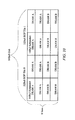
As one example of a partitioned graphics memory, FIG. 1 illustrates a memory system 100 similar to that described in U.S. patent Ser. No. 10/740,229 by Van Dyke et al., the contents of which are hereby incorporated by reference. A memory system 100 for a partitioned memory system 100 includes two or more memory partitions, with the total number of partitions being equal to a power of two, such as four partitions. Each partition P0 115, P1 120, P2 125, and P3 130 is coupled to a memory controller 105 by its own respective data bus 135. Each data bus 135 has a memory byte width, Wp, with an associated packet width for addressing locations within the partition. In accord with a common usage in the graphics industry, a packet is a unit of data transfer.
In turn, each partition may have sub-partitions, such as two sub-partitions SP0 140A and SP1 140B. Each sub-partition 140A and 140B has its own respective sub-bus 148 with a corresponding byte width for sub-packets, Wsp, addressed to a memory location in the sub-partition. Thus, in a single memory access to a partition, Pi, a single memory access may be made to each of its sub-partitions SPi. The sub-partitions are thus the minimum addressable unit of the graphics system. Each sub-partition may, for example, be a double data rate (DDR) dynamic random access memory (DRAM). As an illustrative example, each partition may have 64 data pins whereas each sub-partition 140A or 140B has 32 data pins. This permits, for example, a 64 bit partition to be implemented as two conventional 32 bit memory chips.
The memory controller 105 routes addresses of requests from individual clients of a graphics system to specific partition/sub-partition memory locations. The individual clients may be any component within a graphics processing system that requires access to a graphics memory to read, write, clear, or compress tile data. An arbitration module 150 selects a client 155 or 160.
A partition address routing module 190 maps an address associated with a client (e.g., a read or write request) to a memory location in a partition and its associated sub-partitions. A compression/decompression module 165 is included to compress and decompress tile data to reduce memory bandwidth requirements. A tag module 170 may be included to identify, by a tag (e.g., one or more bits) attributes of the tiles, such as whether a tile holds data in a compressed format. A packing/unpacking state machine 180 and format conversion module 195 are provided to reorganize tile data.
As previously described, partitioning permits the total effective number of DRAM data pins to be increased compared to an individual DRAM. The total effective number of data pins for the partitioned graphics memory is the number of data pins per partition multiplied by the number of partitions. As graphics systems have evolved, the equivalent DRAM memory size of partitioned graphics memories have increased from 128 pins (27) to 256 pins (28) in current generation products. For example, a total DRAM address space corresponding to 256 pins (which is a power of two, i.e., 256=28) may be implemented with four partitions each having 64 DRAM pins.
Conventionally, the number of DRAMs in a partitioned graphics memory is a power of two. As is well known, binary address spaces naturally scale as a power of two. Additionally, many other attributes of a computer system also typically scale as a power of two. As a consequence, conventional partitioned graphics memories utilize a power of two number of partitions (e.g., four) and have a power of two number of DRAMs (e.g., eight DRAMs in a partitioned graphics memory having four partitions and two DRAMs per partition).
However, doubling the number of DRAMs in successive product generations increases costs and also tends to reduce yield due to the larger chip area that is required. Consequently, it would be desirable to support an arbitrary number of partitions.
In light of the above-described problems the apparatus, system and method of the present invention was developed.
SUMMARY OF THE INVENTION
A graphics system utilizes virtual memory pages and has a partitioned graphics memory that includes memory elements. The partitioned graphics memory supports a non-power of two number of operative memory elements. In one implementation, the memory elements are dynamic random access memories (DRAMs) and the graphics system supports having a total number of active DRAMs that is not equal to a power of two. Additionally, a partition swizzling operation is used to adjust the partition numbers associated with individual units of virtual memory allocation on particular virtual memory pages to achieve a selected partition interleaving pattern.
One embodiment of a graphics system includes a partitioned graphics memory having a plurality of partitions each including at least one dynamic random access memory (DRAM). The graphics system includes a graphics processing unit coupled to the partitioned graphics memory. An address translation module in the graphics processing unit performs an address translation to map virtual addresses to physical addresses and determines individual partitions associated with memory accesses for individual units of virtual memory allocation. The graphics system performs partition interleaving in which data for an individual unit of virtual memory allocation is assigned to one partition and different individual units of virtual memory allocation are assigned to different partitions. The graphics system performs a partition swizzling operation to adjust the partition numbers associated with the individual units of virtual memory allocation on particular virtual memory pages to achieve a selected partition interleaving pattern.
BRIEF DESCRIPTION OF THE FIGURES
The invention is more fully appreciated in connection with the following detailed description taken in conjunction with the accompanying drawings, in which:
FIG. 1 is a block diagram of a prior art partitioned graphics memory;
FIG. 2 is a block diagram of a graphics system with a partitioned graphics memory having a non power of two number of partitions according to one embodiment of the present invention;
FIG. 3 is a block diagram of a graphics system with a partitioned graphics memory having a non-power of two number of DRAMs per partition according to one embodiment of the present invention;
FIG. 4 illustrates a memory management unit (MMU) process for determining partition number and DRAM row-column-bank addresses according to one embodiment of the present invention;
FIG. 5 illustrates an exemplary sequence of address translations according to one embodiment of the present invention;
FIG. 6 illustrates an exemplary gob of a block-linear memory format in accordance with one embodiment of the present invention;
FIG. 7 illustrates an exemplary block of a block-linear memory format in accordance with one embodiment of the present invention;
FIG. 8 illustrates an exemplary row of a block-linear memory format in accordance with one embodiment of the present invention;
FIG. 9 illustrates a mapping of a surface in a block-liner memory format in accordance with one embodiment of the present invention;
FIG. 10 illustrates an exemplary gob in accordance with one embodiment of a block-linear memory format;
FIG. 11 illustrates an exemplary gob partition assignment without swizzling in accordance with one embodiment of the present invention;
FIG. 12 illustrates an exemplary gob partition assignment with swizzling in accordance with one embodiment of the present invention; and
FIG. 13 illustrates an exemplary mapping of physical addresses to partition numbers and row-column-bank addresses.
Like reference numerals refer to corresponding parts throughout the several views of the drawings.
DETAILED DESCRIPTION OF THE INVENTION
FIG. 2 illustrates a graphics system 200 in accordance with one embodiment of the present invention. A graphics processing unit 205 includes a memory controller 210 to interface a partitioned graphics memory 250 having memory partitions 255 coupled by respective buses 257 to memory controller 210. Each partition 255, may for example, further include sub-partitions 253 coupled to sub-buses 251 via respective parallel interfaces. Each sub-partition 253 includes a memory element. For example, each sub-partition 253 may include a memory element that is a dynamic random access memory (DRAM). Although DRAM is an exemplary type of memory element, it will be understood throughout the following discussion that it is contemplated that the present invention may be applied to other types of memories. Each DRAM of a sub-partition 253 has parallel interfaces with respect to the other sub-partitions 253 of the same partition 255 such that the total equivalent number of DRAM data pins of each partition 255 scales with the number of sub-partitions 253. For example, a single partition 255 having two sub-partitions 253 each of which are 32 bit DRAMs results in an equivalent 64 bit access word.
Memory controller 210 is capable of interfacing a partitioned memory with a non-power of two number of DRAMs (i.e., the number of operative DRAM memory elements does not equal 2m, where m is an integer). FIG. 2 illustrates an embodiment with a non-power of two number of partitions (e.g., three partitions with two sub-partitions in each partition) such that the total number of DRAMs is not a power of two. In an alternate embodiment illustrated in FIG. 3, each partition includes a non-power of two number of sub-partitions 253 (e.g., three DRAMs) such that the total number of DRAMs is not equal to a power of two.
In one embodiment memory controller 210 is programmable such that it is capable of supporting different numbers of DRAMs, including both a power of two number of DRAMs and a non-power of two number of DRAMs. As one example, memory controller 210 may be designed to support different numbers of partitions (e.g., 1, 2, 3, 4, 5, 6, 7, or 8 partitions) and during assembly programmed to support a particular number of partitions. For example, a non-volatile memory may be written to indicate the number of partitions. The number of partitions may be selected, for example, based on cost constraints or yield considerations. For example, the number of partitions selected as operative (active) partitions may be reduced from a maximum number to account for a manufacturing defect. As one example of a yield consideration, one reason that a non-power of two number of partitions may be used is the case where a chip is nominally designed for four partitions but after manufacture has one defective partition. In this example instead of discarding the die, the defective partition can be disabled and a product with three (a non power-of-two) active partitions shipped. In a performance mode the number of partitions may be selected for different market segments. Similarly, the number of sub-partitions per partition may be based on cost or yield considerations.
Memory controller 210 includes an address translation module 215-A to map memory addresses to particular partitions and row-bank-column addresses within partitions. Memory controller 210 performs address translation on behalf of naïve memory clients 230 that lack an address translation capability. However, it will be understood that a sophisticated memory client 235 may include an address translation module 215-B that performs some or all of the address translation for the sophisticated client.
In one embodiment, graphics system 200 includes a CPU 260 utilizing virtual memory addressing implemented using virtual memory pages 280, paging, page tables, and page table entries (PTEs). A system memory 265 stores a graphics application 270, driver 275, and a page table 280. Virtual memory pages 280 are used for memory management and may, for example, be generated to store data for a graphics surface drawn by graphics application 270. A virtual memory page corresponds to a range of consecutive addresses in a virtual address space, such as a 4 KB page size or a 64 KB page size. Address translation information to map virtual to physical page numbers are stored in page tables associated with individual pages. Individual items in a page table are known as page table entries (PTEs). Examples of a graphics system which utilizes page table entries to provide information on tile storage formats for address translation in a partitioned graphics memory is described in U.S. patent Ser. No. 11/393,621, “Apparatus, System, and Method for Using Page Table Entries in a Graphics System to Provide Storage Format Information For Address Translation,” by Montrym et al., the contents of which are hereby incorporated by reference.
In one embodiment, memory management unit (MMU) logic is used to handle memory access requests and perform address translation from virtual addresses to physical addresses. The virtual address space is divided into pages. Copies of the MMU logic may reside in different locations within the graphics system, depending on the implementation. As illustrated in FIGS. 2 and 3, a copy of the MMU logic may be included in address translation module 215-A. A translation lookaside buffer (TLB) 290 in GPU 205 may be used to cache address translation information to translate virtual page numbers to physical page numbers. Page table entries stored in page tables provide additional information for translating addresses. In particular, in a partitioned graphics memory using DRAMs as the memory elements the physical addresses further need to be translated into partition numbers and the row-column-bank addresses within individual DRAMs.
FIG. 4 illustrates an exemplary MMU process. The MMU maps input graphics coordinates, such as texture (u,v) coordinates or (x,y) surface coordinates to virtual addresses. In one embodiment a virtual memory page can be considered to be a virtual tile, where a virtual tile describes a region of virtual memory with common properties that maps to a contiguous region of physical memory. The virtual address space is divided into virtual tiles which can be either a power of two in size (e.g., 64 KB) or a graphics non-power of two size, depending on the number of DRAMs. The MMU maps the virtual tile address to the location of the virtual tile in physical memory using page table entries.
Depending on a client, a virtual address is computed by applying a mapping (such as a pitch or block-linear mapping) onto the coordinates of the surface mapped. A virtual address is determined based, for example, on a virtual offset. A TLB receives PTE information from virtual memory pages. The MMU maps the virtual tile address bits from the virtual address to the location of the virtual tile in physical memory using the PTEs, The PTEs provide information on the “Kind” of data that is stored, and may include information on the data storage formats. Additionally, in one embodiment the PTEs provide information used to generate a partition number and a row-bank-column (RBC) address, such as partition stride, partition swizzle, partition offset or bank swizzle. To map virtual addresses to physical addresses, the low order bits of the virtual address may be used as low order bits of the physical address. High order bits of the virtual address may be used as keys into address translation tables to determine the higher order bits of the physical address.
In one embodiment, the MMU maps the virtual tile address bits from the virtual address to the location of the virtual tile in memory using the PTEs. The remainder of the bits from the virtual address are then combined with the address of the virtual tile in physical memory to compute the physical address associated with the virtual address requested. As an illustrative example, in one embodiment of a 64 KB virtual tile, bits [7,0] specify the byte within a 256 B physical region, bits [15:8] specify a 256 B physical region within the 64 KB virtual tile, and bits [39:16] specify the virtual tile address.
In one embodiment, the MMU logic utilizes one or more modulo operations to perform a partition assignment. A modulo operation is an operation in which for two integers a and n, the operation a modulo n, the result is the remainder after division of a by n. The modulo operation is often represented by the “%” character. A modulo operation may be used to “cycle” physical memory addresses assigned to a partition number or a sub-partition number. That is, one or more modulo operations may be performed on appropriately scaled sets of physical memory addresses to assign chunks of physical memory address to partitions or sub-partitions in a cyclic order. For example, a partition number can be assigned using a modulo operation in which the partition number is based on a subset of physical address of the virtual memory page modulo the number of partitions with appropriate scaling, as described below in more detail. In one embodiment a row-column-bank address is determined by taking a select set of physical address bits divided by the number of partitions.
FIG. 5 illustrates in more detail an exemplary sequence of address translation operations. A region of a graphics surface is generated by a drawing engine 505 and has (x, y, z) coordinates (for the case that graphics surface region is a two dimensional surface, it has (x, y) coordinates). A first address translation 510 is performed to map the graphics surface region to a one-dimensional virtual address (VA) space. The first address translation may comprise a conventional pitch memory format. However, as described in U.S. patent Ser. No. 11/393,621, first address translation 510 may alternatively comprise a block-linear format to generate virtual addresses, which is described below in more detail. A second address translation 520 is performed to translate the virtual address to a physical address (PA). For example, upper bits of the virtual address may be used to lookup a page number and lower bits may be used to form the physical address, where the physical address is a unique number for each byte in memory. A third address translation 530 generates a raw address from the physical address. The raw address includes the collection of fields needed to uniquely locate each byte in the DRAMs. In particular, the raw address includes a partition number (and also sub-partition number, if a sub-partition is included) and a row-bank-column (RBC addresses) within a particular DRAM. The third translation 530 to determine the raw address may, for example, utilize information in a page table entry specifying a data “kind” describing one or more formats for packing tile data (e.g., intra-tile packing). That is the page table entry provides auxiliary information describing the organization of raw graphics data in memory. As examples, a PTE may comprise fields indicating a compression mode, a multi-sample format, and one or more tile data formats. As described below in more detail, in one embodiment a PTE may also include fields to support utilization of non-power of two numbers of DRAMs, such as a partition stride field to indicate units of contiguous memory stored within each partition, a partition offset field to adjust the partition number for the start of a page, and a bank swizzle field to perform bank swizzling for non-power of two numbers of DRAMs. It will also be understood that it is contemplated that more generally PTE fields may be provided to provide other types of information useful for performing address translation to optimize the use of a partitioned memory having a non-power of two number of DRAMs.
In one embodiment of a block-linear memory format a graphics surface is mapped according to a hierarchical sequence of nested loops of gobs (sub-blocks), blocks, rows of blocks, and a whole surface to perform the mapping between spatial coordinates to virtual addresses. The gob is a selected number of lines tall (e.g., 4 or 8, depending on the implementation) and has a selected byte width (e.g., 64 B) A gob also preferably corresponds to an integer number of DRAM atoms for accessing an individual DRAM. A packing choice may be specified by a page kind field in a page table entry. As illustrated in FIG. 6, a gob corresponds to a rectangular region of memory, such as 256 bytes in virtual address space, which is a minimum unit of allocation of a block-linear surface in virtual address space. An individual gob may also correspond in size to that of a tile or small number of tiles. If a pixel requires 4 B of storage, a 256 B gob represents a 16 by 4 pixel region of a 2D surface. A gob is preferably 256 bytes aligned to 256B such that a gob never crosses a MMU page boundary. As illustrated in FIG. 7, a set of gobs are organized into a block. In particular, in one embodiment after the byte addresses of one gob are traversed the next gob down the block is traversed and so on until the block has been completely traversed. Blocks are further arranged in a specified order into rows, as illustrated in FIG. 8. Thus, after one block is traversed the next block is traversed in the row. Finally, as illustrated in FIG. 9, a whole surface is traversed through a sequence of rows. As previously described, a gob typically corresponds to one or more tiles and may be implemented with different numbers of lines. FIG. 10 illustrates a 64B×8 line Gob corresponding to two tiles. Individual sub-sections of a Gob may be assigned to different sub-partitions A or B.
The block-linear memory format maps graphics surfaces in a way that preserves attributes of the source data and which facilitates efficient access of data. In a block-linear format the block attributes may be selected to facilitate utilizing a non-power number of two DRAMs. As previously described in one embodiment virtual memory pages may be a power of two size or a non power of two size. In one embodiment the block height is always a power of two (e.g., 20, 21, 22, 24) number of gobs but the block width can be an integer number of gobs (e.g., 1, 2 or 3). In this implementation the virtual memory page width varies with the number of partitions.
As previously described, PTE fields may be included to provide information for a MMU to determine a partition number. One example of a PTE is a partition stride. The partition stride is a unit of contiguous virtual/physical memory contained within an individual partition. The partition stride determines how frequently the partition number is stepped as gobs are traversed. For example, the partition stride may correspond to one gob (256B) or a small number of gobs (e.g., four gobs or 1024B). Thus, individual gob-sized regions of contiguous virtual/physical memory addresses are mapped to individual partitions. A consequence of the partition stride is that gobs are interleaved amongst the partitions based, in part, on the partition stride. Additionally, as previously described a PTE may be included for a partition offset. The partition offset is a pre-computed partition number for the location at the start of the page in physical memory. Thus, the partition offset determines a starting partition for determining a partition number.
As previously described, MMU logic may use PTE information to determine a partition number based on a modulo operation. For example, with 1024B partitions an exemplary formula for mapping a physical address to a partition number (e.g., Partition [2:0], indicating a partition number) based on a modulo operation on upper bits of the address with respect to the number of partitions is as follows:
Partition[2:0]=(Physical Address[n-1:0])/(Partition Stride)) % (# partitions)
With a partition stride defined to be 256B or 1024B in a 64 KB virtual memory page, the equation simplifies to:
256B Partitions: Partition[2:0]=({Physical Address[n-1:8]}) % (# partitions)
1024B Partitions: Partition[2:0]=(Physical Address[n-1:10]) % (# partitions)
Where the modulo operation is performed with respect to a subset of the physical address bits and scaled appropriately by the partition stride to determine a partition number, which may correspond to bits specifying the partition number.
As previously described, row-column-bank addresses may be determined by MMU logic by analyzing a quotient of selected physical bits with respect to the number of partitions. In one implementation the nomenclature bank[b-1:0] denotes DRAM internal bank address bits and extbank denotes banks of DRAM chips. The RBC address (RBC_ADR) at the partition can be expressed by the following equations by examining a quotient of a set of physical address bits divided by the number of partitions. In the equations, the first expression is a concatenation of row bits, external bank “extbank” bits (corresponding to DRAMs operated in parallel), and internal bank bits and column “col” bits:
256B Partition:
{row[r-1:0], extbank, bank[b-1:0], col[c-1:5]}=int(PA[n-1:8]}/(# partitions))//==RBC_ADR at partition
1024B Partition:
{row[r-1:0], extbank, bank[b-1:0], col[c-1:5]}=if (problem page crossing region)
then
int(PA[n-1:8]/(# partitions))//==RBC_ADR
else
{int(PA[n-1:10]/(# partitions)), PA[9:8]}//==RBC_ADR
The partition mapping is also preferably selected to support an arbitrary number of partitions such that the GPU can be used with graphics memory having a power of two number of partitions and also a non power of two number of partitions. A potential problem is achieving effective load balancing, particularly for power-of-two numbers of partitions. In the most straightforward implementation of a block linear format, gobs are organized vertically into column-like blocks before stepping horizontally. Note that as described below in more detail, an interleave between partitions vertically inside a virtual memory page mapping may be performed such that no adjacent gobs have the same number vertically. However, a problem that is encountered if a block has a power of two number of gobs (e.g., four gobs) and there are a power-of-two number of partitions, rows of gobs will be assigned to the same partition number. This is undesirable for the case of clients that access data in horizontal patterns since only one partition would be utilized, reducing memory access efficiency. In particular, it is generally desirable for common memory access patterns that the desired data be spread amongst the partitions so that the data can be efficiently accessed from multiple partitions in a minimum number of clock cycles.
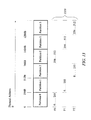
In one embodiment an additional partition swizzling operation is performed to improve the assignment of partitions. In particular, the swizzling operation may be used to improve the abutment of gobs on virtual memory pages, particularly for the case of a power of two number of partitions. FIG. 11 illustrates an alignment of gobs on a virtual memory page that would occur without swizzling for the case of four partitions (0, 1, 2, and 3). The partition number associated with each gob is illustrated. Since there is a power of two number of partitions, entire rows of gobs are assigned to the same partition number. As previously described this in undesirable for clients that access data in horizontal patterns. A hash operation may be used to swizzle the partition assignments to achieve a better pattern of gobs. FIG. 12 illustrates an alignment of gobs on a virtual memory page with swizzling to achieve a checkerboard pattern of gob partition assignments.
In one embodiment, a swizzling operation may utilize an XOR operation on selected address bits of page, such as on bits 0 to bit 15 of the 16 bits of a 64 KB page. These sixteen bits correspond to a region of contiguous addresses within one virtual memory page. That is, the swizzling is performed to reorganize particular virtual memory pages to improve abutment. The swizzling may also use the partition offset PTE to assist in determining a useful abutment. The swizzling will also depend upon the number of partitions used. The equations below describe an exemplary set of swizzling operations to interleave 256B partitions depending upon the number of partitions using XOR operation (^) on the 16 physical address (PA) bits 0 to 15 associated with a virtual memory page:
1 Partition:
Partition[2:0]=0
2 Partitions:
Partition[2:0]={0,0, PA[8] ^ PA[9] ^ PA[10] ^ PA[11] ^ PA[12] ^ PA[13]}
3 Partitions:
Partition[2:0]=(PA[15:8]+(Partition Offset)) % 3
4 Partitions:
Partition[2:0]=(PA[14]+PA[13:12]+PA[11:10]+PA[9:8]) % 4
5 Partitions:
Partition[2:0]=(PA[15:8]+(Partition Offset)) % 5
6 Partitions:
Partition[2:0] ((PA[15:8]+(Partition Offset)) % 6) ^{0,0, swz[4]^swz[3]^swz[2]^swz[1]^swz[0]}
where swz[4:0]=int(PA[n-1:8]/6)%32
As previously described, in one embodiment a PTE field may be included for bank swizzling. Bank swizzling of the physical bank bits permits the banks to be optimally aligned to prevent DRAM page faults. For example, consider a 4 bank pattern and an 8 bank pattern.
Without bank swizzling, the bank patterns are as follows:
4 bank pattern: 0 1 2 3
8 bank pattern: 0 1 2 3 4 5 6 7
Since a bank may span all partitions, partition swizzling may not solve the same bank abutment problem. Systems with power-of-two number of partitions will have mapping patterns similar to those illustrated in FIG. 11.
With bank swizzling, the bank patterns are swizzled. Exemplary swizzled 4 bank and 8 bank patterns are as follows:
4 bank pattern (swizzled): 2130
8 bank pattern (swizzled): 4 6 1 3 5 7 0 2
As previously described in regards to FIG. 3, in one embodiment each partition includes a non-power of two number of DRAMs, such as three DRAMs. A modulo technique may be used to map physical addresses to a non-power of two number of sub-partitions. For example with three DRAM sub-partitions each having a 16B access for a 48B total, a first modulo operation may be used to take the physical address for the partition modulo by 48 B and then the result divided by 48 B to select the partition. Within the 48 B of the selected partition, a second modulo operation, a modulo three, would determine the DRAM sub-partition. The RBC address within the sub-partition is then determined by dividing the physical address by 48 B.
FIG. 13 illustrates some of the aspects of determining partition numbers and RBC addresses. The physical address space progresses from zero to some upper number. In this example, the mapping of physical addresses to partition numbers P0, P1, and P2 is based on a partition stride of 256B. As indicated in inset 1310, the address translation between physical addresses and raw DRAM addresses has to account for the fact that physical addresses are assigned to the partitions in a sequence, i.e. partition 0 (P0) receives bytes 0 to 255 for one range of physical addresses and then bytes 256 to 512 for a separate range of physical addresses. Additionally, the address translation will depend upon which partition is selected to be the first partition of a page (in this example, partition P0). The partition offset or starting partition may be calculated or stored in the PTE. It can be understood from FIG. 13 that a modulo operation based on the number of partitions, a partition stride, and a partition offset is an efficient way to translate physical addresses to partition number. However, it will be understood that other address translation methods are also contemplated to determine partition number and RBC addresses.
The foregoing description, for purposes of explanation, used specific nomenclature to provide a thorough understanding of the invention. However, it will be apparent to one skilled in the art that specific details are not required in order to practice the invention. Thus, the foregoing descriptions of specific embodiments of the invention are presented for purposes of illustration and description. They are not intended to be exhaustive or to limit the invention to the precise forms disclosed; obviously, many modifications and variations are possible in view of the above teachings. The embodiments were chosen and described in order to best explain the principles of the invention and its practical applications, they thereby enable others skilled in the art to best utilize the invention and various embodiments with various modifications as are suited to the particular use contemplated. It is intended that the following claims and their equivalents define the scope of the invention.

Claims (20)

1. A graphics system, comprising:
a partitioned graphics memory having a plurality of independently addressable partitions each including at least one dynamic random access memory (DRAM), with a total number of operative DRAMs being a non power of two number, and at least one of said partitions including multiple DRAMs;
a graphics processing unit coupled to said partitioned graphics memory;
an address translation module in said graphics processing unit performing an address translation mapping virtual addresses to physical addresses and determining individual partitions associated with memory accesses for individual units of virtual memory allocation, said address translation module configured to perform a first modulo operation to select an individual partition in said partitioned graphics memory, said address translation module configured to perform a second modulo operation to select an individual DRAM included in said selected partition;
said graphics system performing partition interleaving in which data for an individual unit of virtual memory allocation is assigned to one partition and different individual units of virtual memory allocation are assigned to different partitions;
said graphics system performing a partition swizzling operation to adjust the partition numbers associated with said individual units of virtual memory allocation on particular virtual memory pages to achieve a selected partition interleaving pattern.
2. The graphics system of claim 1, wherein said selected partition interleaving pattern is a checkerboard pattern that prevents rows or columns of said individual units of virtual memory allocation on a virtual page from being assigned to the same partition.
3. The graphics system of claim 1, wherein said swizzling operation is based on the number of partitions in said partitioned memory such that said graphics system supports both a power of two number of partitions and a non power of two number of partitions.
4. The graphics system of claim 1, wherein said partition interleaving is based on the total number of said plurality of partitions and a partition offset indicating the first partition for a particular virtual memory page.
5. The graphics system of claim 4, wherein a partition offset is either stored as part of a page table entry or calculated at translation time.
6. The graphics system of claim 4, wherein said partition interleaving is further based on partition stride indicative of an integer number of individual units of virtual memory allocation.
7. The graphics system of claim 6, wherein said partition stride is stored as a page table entry.
8. The graphics system of claim 1, wherein said graphics system further performs bank swizzling to optimize bank utilization.
9. The graphics system of claim 1, wherein a memory format organizes said individual units of virtual memory allocation on particular virtual memory pages into blocks, said blocks further organized into rows.
10. The graphics system of claim 1, wherein said address translation module is configured to perform said first modulo operation based on a subset of physical address bits and a total number of partitions to arrive at a partition number, and said selected partition includes a non power of two number of DRAMs.
11. A graphics system, comprising:
a partitioned graphics memory having a plurality of independently addressable partitions each including at least one dynamic random access memory (DRAM), with a total number of operative DRAMs being a non power of two number, and at least one of said partitions including multiple DRAMs;
a central processing unit (CPU) utilizing virtual memory addressing in which at least one type of graphics data is represented on virtual pages as virtual tiles having units of virtual memory allocation organized according to a memory format; and
a graphics processing unit coupled to said partitioned graphics memory;
an address translation module in said graphics processing unit performing an address translation mapping physical addresses to individual partitions and DRAM addresses within partitions, said address translation module being programmable to specify a number of partitions in said partitioned graphics memory, said address translation being based on said specified number of partitions, said address translation module configured to perform a first modulo operation to select an individual partition in said partitioned graphics memory, said address translation module configured to perform a second modulo operation to select an individual DRAM included in said selected partition;
said graphics system performing partition interleaving in which data for an individual unit of virtual memory allocation is assigned to one partition and different individual units of virtual memory allocation are assigned to different partitions;
said graphics system performing a partition swizzling operation to adjust the partition numbers associated with said individual units of virtual memory allocation on particular virtual memory pages to achieve a selected partition interleaving pattern.
12. The graphics system of claim 11, wherein said selected partition interleaving pattern is a checkerboard pattern that prevents rows of said individual units of virtual memory allocation on a virtual page from being assigned to the same partition.
13. The graphics system of claim 11, wherein said swizzling operation is based on the specified number of partitions in said partitioned memory such that said graphics system supports both a power of two number of partitions and a non power of two number of partitions.
14. The graphics system of claim 11, wherein said partition interleaving is based on the specified number of partitions and a partition offset indicating the first partition for a particular virtual memory page.
15. The graphics system of claim 14, wherein said partition offset is stored as part of a page table entry.
16. The graphics system of claim 14, wherein said partition interleaving is further based on partition stride indicative of an integer number of individual units of virtual memory allocation.
17. The graphics system of claim 16, wherein said partition stride is stored as part of a page table entry.
18. The graphics system of claim 11, wherein said graphics system further performs bank swizzling to optimize bank utilization.
19. The graphics system of claim 11, wherein said memory format organizes said individual units of virtual memory allocation into blocks, said blocks further organized into rows.
20. The graphics system of claim 11, further comprising a non-volatile memory to store an indication corresponding to said specified number of partitions, and said specified number of partitions is different from a total number of partitions in said partitioned graphics memory.
US11/538,755 2006-10-04 2006-10-04 Graphics system with virtual memory pages and non-power of two number of memory elements Active 2029-07-19 US8072463B1 (en)

Priority Applications (1)

Application Number Priority Date Filing Date Title
US11/538,755 US8072463B1 (en) 2006-10-04 2006-10-04 Graphics system with virtual memory pages and non-power of two number of memory elements

Applications Claiming Priority (1)

Application Number Priority Date Filing Date Title
US11/538,755 US8072463B1 (en) 2006-10-04 2006-10-04 Graphics system with virtual memory pages and non-power of two number of memory elements

Publications (1)

Publication Number Publication Date
US8072463B1 true US8072463B1 (en) 2011-12-06

Family

ID=45034424

Family Applications (1)

Application Number Title Priority Date Filing Date
US11/538,755 Active 2029-07-19 US8072463B1 (en) 2006-10-04 2006-10-04 Graphics system with virtual memory pages and non-power of two number of memory elements

Country Status (1)

Country Link
US (1) US8072463B1 (en)

Cited By (18)

* Cited by examiner, † Cited by third party
Publication number Priority date Publication date Assignee Title
US20110078359A1 (en) * 2009-09-25 2011-03-31 Van Dyke James M Systems and Methods for Addressing Physical Memory
WO2013184252A1 (en) * 2012-06-04 2013-12-12 Qualcomm Incorporated Memory channel selection in a multi-channel memory system
US20150089168A1 (en) * 2013-09-20 2015-03-26 Advanced Micro Devices, Inc. Nested channel address interleaving
US20150294435A1 (en) * 2014-04-09 2015-10-15 Intel Corporation Banked memory access efficiency by a graphics processor
TWI514146B (en) * 2012-12-12 2015-12-21 Nvidia Corp Address bit remapping scheme to reduce access granularity of dram accesses
US9299124B2 (en) 2012-06-07 2016-03-29 Qualcomm Incorporated Padding for multi-channel memory
US9519578B1 (en) 2013-01-28 2016-12-13 Radian Memory Systems, Inc. Multi-array operation support and related devices, systems and software
US9542118B1 (en) * 2014-09-09 2017-01-10 Radian Memory Systems, Inc. Expositive flash memory control
US10127627B2 (en) * 2015-09-23 2018-11-13 Intel Corporation Mapping graphics resources to linear arrays using a paging system
US10445229B1 (en) 2013-01-28 2019-10-15 Radian Memory Systems, Inc. Memory controller with at least one address segment defined for which data is striped across flash memory dies, with a common address offset being used to obtain physical addresses for the data in each of the dies
US10552058B1 (en) 2015-07-17 2020-02-04 Radian Memory Systems, Inc. Techniques for delegating data processing to a cooperative memory controller
US10552085B1 (en) 2014-09-09 2020-02-04 Radian Memory Systems, Inc. Techniques for directed data migration
US10642505B1 (en) 2013-01-28 2020-05-05 Radian Memory Systems, Inc. Techniques for data migration based on per-data metrics and memory degradation
US10740247B2 (en) * 2016-08-11 2020-08-11 Huawei Technologies Co., Ltd. Method for accessing entry in translation lookaside buffer TLB and processing chip
US10838853B1 (en) 2013-01-28 2020-11-17 Radian Memory Systems, Inc. Nonvolatile memory controller that defers maintenance to host-commanded window
US11175984B1 (en) 2019-12-09 2021-11-16 Radian Memory Systems, Inc. Erasure coding techniques for flash memory
US11249652B1 (en) 2013-01-28 2022-02-15 Radian Memory Systems, Inc. Maintenance of nonvolatile memory on host selected namespaces by a common memory controller
US20230045443A1 (en) * 2021-08-02 2023-02-09 Nvidia Corporation Performing load and store operations of 2d arrays in a single cycle in a system on a chip

Citations (24)

* Cited by examiner, † Cited by third party
Publication number Priority date Publication date Assignee Title
US5129060A (en) * 1987-09-14 1992-07-07 Visual Information Technologies, Inc. High speed image processing computer
US5321809A (en) 1992-09-11 1994-06-14 International Business Machines Corporation Categorized pixel variable buffering and processing for a graphics system
US5384912A (en) * 1987-10-30 1995-01-24 New Microtime Inc. Real time video image processing system
US5696927A (en) 1995-12-21 1997-12-09 Advanced Micro Devices, Inc. Memory paging system and method including compressed page mapping hierarchy
US5781200A (en) 1996-08-08 1998-07-14 Ulsi Systems Tile memory mapping for increased throughput in a dual bank access DRAM
US5790130A (en) * 1995-06-08 1998-08-04 Hewlett-Packard Company Texel cache interrupt daemon for virtual memory management of texture maps
US6006318A (en) * 1995-08-16 1999-12-21 Microunity Systems Engineering, Inc. General purpose, dynamic partitioning, programmable media processor
US6070227A (en) * 1997-10-31 2000-05-30 Hewlett-Packard Company Main memory bank indexing scheme that optimizes consecutive page hits by linking main memory bank address organization to cache memory address organization
US6092124A (en) 1998-04-17 2000-07-18 Nvidia Corporation Method and apparatus for accelerating the rendering of images
US6301649B1 (en) * 1997-04-07 2001-10-09 Oki Electric Industry Co., Ltd. Semiconductor circuit with address translation circuit that enables quick serial access in row or column directions
US6344852B1 (en) * 1999-03-17 2002-02-05 Nvidia Corporation Optimized system and method for binning of graphics data
US6381668B1 (en) 1997-03-21 2002-04-30 International Business Machines Corporation Address mapping for system memory
US6405286B2 (en) * 1998-07-31 2002-06-11 Hewlett-Packard Company Method and apparatus for determining interleaving schemes in a computer system that supports multiple interleaving schemes
US6523104B2 (en) 2001-07-13 2003-02-18 Mips Technologies, Inc. Mechanism for programmable modification of memory mapping granularity
US20030046501A1 (en) * 2001-09-04 2003-03-06 Schulz Jurgen M. Method for interleaving memory
US6661423B2 (en) 2001-05-18 2003-12-09 Sun Microsystems, Inc. Splitting grouped writes to different memory blocks
US20040080512A1 (en) * 2002-10-24 2004-04-29 Mccormack Joel James Efficient hardware a-buffer using three-dimensional allocation of fragment memory
US20040093457A1 (en) * 2002-11-12 2004-05-13 Heap Mark A. Mapping addresses to memory banks based on at least one mathematical relationship
US6825847B1 (en) 2001-11-30 2004-11-30 Nvidia Corporation System and method for real-time compression of pixel colors
US6853382B1 (en) 2000-10-13 2005-02-08 Nvidia Corporation Controller for a memory system having multiple partitions
US6999088B1 (en) * 2003-12-23 2006-02-14 Nvidia Corporation Memory system having multiple subpartitions
US20070126756A1 (en) * 2005-12-05 2007-06-07 Glasco David B Memory access techniques providing for override of page table attributes
US7286134B1 (en) 2003-12-17 2007-10-23 Nvidia Corporation System and method for packing data in a tiled graphics memory
US7620793B1 (en) * 2006-08-28 2009-11-17 Nvidia Corporation Mapping memory partitions to virtual memory pages

Patent Citations (24)

* Cited by examiner, † Cited by third party
Publication number Priority date Publication date Assignee Title
US5129060A (en) * 1987-09-14 1992-07-07 Visual Information Technologies, Inc. High speed image processing computer
US5384912A (en) * 1987-10-30 1995-01-24 New Microtime Inc. Real time video image processing system
US5321809A (en) 1992-09-11 1994-06-14 International Business Machines Corporation Categorized pixel variable buffering and processing for a graphics system
US5790130A (en) * 1995-06-08 1998-08-04 Hewlett-Packard Company Texel cache interrupt daemon for virtual memory management of texture maps
US6006318A (en) * 1995-08-16 1999-12-21 Microunity Systems Engineering, Inc. General purpose, dynamic partitioning, programmable media processor
US5696927A (en) 1995-12-21 1997-12-09 Advanced Micro Devices, Inc. Memory paging system and method including compressed page mapping hierarchy
US5781200A (en) 1996-08-08 1998-07-14 Ulsi Systems Tile memory mapping for increased throughput in a dual bank access DRAM
US6381668B1 (en) 1997-03-21 2002-04-30 International Business Machines Corporation Address mapping for system memory
US6301649B1 (en) * 1997-04-07 2001-10-09 Oki Electric Industry Co., Ltd. Semiconductor circuit with address translation circuit that enables quick serial access in row or column directions
US6070227A (en) * 1997-10-31 2000-05-30 Hewlett-Packard Company Main memory bank indexing scheme that optimizes consecutive page hits by linking main memory bank address organization to cache memory address organization
US6092124A (en) 1998-04-17 2000-07-18 Nvidia Corporation Method and apparatus for accelerating the rendering of images
US6405286B2 (en) * 1998-07-31 2002-06-11 Hewlett-Packard Company Method and apparatus for determining interleaving schemes in a computer system that supports multiple interleaving schemes
US6344852B1 (en) * 1999-03-17 2002-02-05 Nvidia Corporation Optimized system and method for binning of graphics data
US6853382B1 (en) 2000-10-13 2005-02-08 Nvidia Corporation Controller for a memory system having multiple partitions
US6661423B2 (en) 2001-05-18 2003-12-09 Sun Microsystems, Inc. Splitting grouped writes to different memory blocks
US6523104B2 (en) 2001-07-13 2003-02-18 Mips Technologies, Inc. Mechanism for programmable modification of memory mapping granularity
US20030046501A1 (en) * 2001-09-04 2003-03-06 Schulz Jurgen M. Method for interleaving memory
US6825847B1 (en) 2001-11-30 2004-11-30 Nvidia Corporation System and method for real-time compression of pixel colors
US20040080512A1 (en) * 2002-10-24 2004-04-29 Mccormack Joel James Efficient hardware a-buffer using three-dimensional allocation of fragment memory
US20040093457A1 (en) * 2002-11-12 2004-05-13 Heap Mark A. Mapping addresses to memory banks based on at least one mathematical relationship
US7286134B1 (en) 2003-12-17 2007-10-23 Nvidia Corporation System and method for packing data in a tiled graphics memory
US6999088B1 (en) * 2003-12-23 2006-02-14 Nvidia Corporation Memory system having multiple subpartitions
US20070126756A1 (en) * 2005-12-05 2007-06-07 Glasco David B Memory access techniques providing for override of page table attributes
US7620793B1 (en) * 2006-08-28 2009-11-17 Nvidia Corporation Mapping memory partitions to virtual memory pages

Non-Patent Citations (3)

* Cited by examiner, † Cited by third party
Title
Hsu, Joni, Final Office Action issued to U.S. Appl. No. 11/538,741, Mar. 25, 2010, 18 pages.
Hsu, Joni, Non-final Office Action issued to U.S. Appl. No. 11/538,741, Sep. 15, 2009, 15 pages.
Hsu, Joni, Non-final Office Action issued to U.S. Appl. No. 11/556,148, Sep. 29, 2009, 13 pages.

Cited By (88)

* Cited by examiner, † Cited by third party
Publication number Priority date Publication date Assignee Title
US20110078359A1 (en) * 2009-09-25 2011-03-31 Van Dyke James M Systems and Methods for Addressing Physical Memory
US9348751B2 (en) * 2009-09-25 2016-05-24 Nvidia Corporation System and methods for distributing a power-of-two virtual memory page across a non-power-of two number of DRAM partitions
WO2013184252A1 (en) * 2012-06-04 2013-12-12 Qualcomm Incorporated Memory channel selection in a multi-channel memory system
US9009441B2 (en) 2012-06-04 2015-04-14 Qualcomm Incorporated Memory channel selection in a multi-channel memory
US9299124B2 (en) 2012-06-07 2016-03-29 Qualcomm Incorporated Padding for multi-channel memory
US10020036B2 (en) 2012-12-12 2018-07-10 Nvidia Corporation Address bit remapping scheme to reduce access granularity of DRAM accesses
TWI514146B (en) * 2012-12-12 2015-12-21 Nvidia Corp Address bit remapping scheme to reduce access granularity of dram accesses
US11709772B1 (en) 2013-01-28 2023-07-25 Radian Memory Systems, Inc. Storage system with multiplane segments and cooperative flash management
US11354235B1 (en) 2013-01-28 2022-06-07 Radian Memory Systems, Inc. Memory controller for nonvolatile memory that tracks data write age and fulfills maintenance requests targeted to host-selected memory space subset
US9519578B1 (en) 2013-01-28 2016-12-13 Radian Memory Systems, Inc. Multi-array operation support and related devices, systems and software
US11899575B1 (en) 2013-01-28 2024-02-13 Radian Memory Systems, Inc. Flash memory system with address-based subdivision selection by host and metadata management in storage drive
US11868247B1 (en) 2013-01-28 2024-01-09 Radian Memory Systems, Inc. Storage system with multiplane segments and cooperative flash management
US11216365B1 (en) 2013-01-28 2022-01-04 Radian Memory Systems, Inc. Maintenance of non-volaitle memory on selective namespaces
US9710377B1 (en) 2013-01-28 2017-07-18 Radian Memory Systems, Inc. Multi-array operation support and related devices, systems and software
US11762766B1 (en) 2013-01-28 2023-09-19 Radian Memory Systems, Inc. Storage device with erase unit level address mapping
US11188457B1 (en) 2013-01-28 2021-11-30 Radian Memory Systems, Inc. Nonvolatile memory geometry export by memory controller with variable host configuration of addressable memory space
US11249652B1 (en) 2013-01-28 2022-02-15 Radian Memory Systems, Inc. Maintenance of nonvolatile memory on host selected namespaces by a common memory controller
US11748257B1 (en) 2013-01-28 2023-09-05 Radian Memory Systems, Inc. Host, storage system, and methods with subdivisions and query based write operations
US10445229B1 (en) 2013-01-28 2019-10-15 Radian Memory Systems, Inc. Memory controller with at least one address segment defined for which data is striped across flash memory dies, with a common address offset being used to obtain physical addresses for the data in each of the dies
US11740801B1 (en) 2013-01-28 2023-08-29 Radian Memory Systems, Inc. Cooperative flash management of storage device subdivisions
US11314636B1 (en) 2013-01-28 2022-04-26 Radian Memory Systems, Inc. Nonvolatile/persistent memory drive with address subsections configured for respective read bandwidths
US10642505B1 (en) 2013-01-28 2020-05-05 Radian Memory Systems, Inc. Techniques for data migration based on per-data metrics and memory degradation
US11704237B1 (en) 2013-01-28 2023-07-18 Radian Memory Systems, Inc. Storage system with multiplane segments and query based cooperative flash management
US11681614B1 (en) 2013-01-28 2023-06-20 Radian Memory Systems, Inc. Storage device with subdivisions, subdivision query, and write operations
US10838853B1 (en) 2013-01-28 2020-11-17 Radian Memory Systems, Inc. Nonvolatile memory controller that defers maintenance to host-commanded window
US10884915B1 (en) 2013-01-28 2021-01-05 Radian Memory Systems, Inc. Flash memory controller to perform delegated move to host-specified destination
US11640355B1 (en) 2013-01-28 2023-05-02 Radian Memory Systems, Inc. Storage device with multiplane segments, cooperative erasure, metadata and flash management
US11544183B1 (en) 2013-01-28 2023-01-03 Radian Memory Systems, Inc. Nonvolatile memory controller host-issued address delimited erasure and memory controller remapping of host-address space for bad blocks
US11487656B1 (en) 2013-01-28 2022-11-01 Radian Memory Systems, Inc. Storage device with multiplane segments and cooperative flash management
US10983907B1 (en) 2013-01-28 2021-04-20 Radian Memory Systems, Inc. Nonvolatile memory controller that supports host selected data movement based upon metadata generated by the nonvolatile memory controller
US10996863B1 (en) 2013-01-28 2021-05-04 Radian Memory Systems, Inc. Nonvolatile memory with configurable zone/namespace parameters and host-directed copying of data across zones/namespaces
US11487657B1 (en) 2013-01-28 2022-11-01 Radian Memory Systems, Inc. Storage system with multiplane segments and cooperative flash management
US11334479B1 (en) 2013-01-28 2022-05-17 Radian Memory Systems, Inc. Configuring write parallelism for namespaces in a nonvolatile memory controller
US11354234B1 (en) 2013-01-28 2022-06-07 Radian Memory Systems, Inc. Memory controller for nonvolatile memory with targeted erase from host and write destination selection based on wear
US11347638B1 (en) 2013-01-28 2022-05-31 Radian Memory Systems, Inc. Nonvolatile memory controller with data relocation and host-triggered erase
US11347639B1 (en) 2013-01-28 2022-05-31 Radian Memory Systems, Inc. Nonvolatile memory controller with host targeted erase and data copying based upon wear
US11074175B1 (en) 2013-01-28 2021-07-27 Radian Memory Systems, Inc. Flash memory controller which assigns address and sends assigned address to host in connection with data write requests for use in issuing later read requests for the data
US11080181B1 (en) 2013-01-28 2021-08-03 Radian Memory Systems, Inc. Flash memory drive that supports export of erasable segments
US20150089168A1 (en) * 2013-09-20 2015-03-26 Advanced Micro Devices, Inc. Nested channel address interleaving
US9141541B2 (en) * 2013-09-20 2015-09-22 Advanced Micro Devices, Inc. Nested channel address interleaving
US20150294435A1 (en) * 2014-04-09 2015-10-15 Intel Corporation Banked memory access efficiency by a graphics processor
KR101855379B1 (en) 2014-04-09 2018-05-09 인텔 코포레이션 Improved banked memory access efficiency by a graphics processor
US9632801B2 (en) * 2014-04-09 2017-04-25 Intel Corporation Banked memory access efficiency by a graphics processor
US11221961B1 (en) 2014-09-09 2022-01-11 Radian Memory Systems, Inc. Configuration of nonvolatile memory as virtual devices with user defined parameters
US11449436B1 (en) 2014-09-09 2022-09-20 Radian Memory Systems, Inc. Storage system with division based addressing and cooperative flash management
US11221959B1 (en) 2014-09-09 2022-01-11 Radian Memory Systems, Inc. Nonvolatile memory controller supporting variable configurability and forward compatibility
US11226903B1 (en) 2014-09-09 2022-01-18 Radian Memory Systems, Inc. Nonvolatile/persistent memory with zone mapped to selective number of physical structures and deterministic addressing
US11237978B1 (en) 2014-09-09 2022-02-01 Radian Memory Systems, Inc. Zone-specific configuration of maintenance by nonvolatile memory controller
US11914523B1 (en) 2014-09-09 2024-02-27 Radian Memory Systems, Inc. Hierarchical storage device with host controlled subdivisions
US11269781B1 (en) 2014-09-09 2022-03-08 Radian Memory Systems, Inc. Programmable configuration of zones, write stripes or isolated regions supported from subset of nonvolatile/persistent memory
US11275695B1 (en) 2014-09-09 2022-03-15 Radian Memory Systems, Inc. Persistent/nonvolatile memory with address translation tables by zone
US11288203B1 (en) 2014-09-09 2022-03-29 Radian Memory Systems, Inc. Zones in nonvolatile memory formed along die boundaries with independent address translation per zone
US11307995B1 (en) 2014-09-09 2022-04-19 Radian Memory Systems, Inc. Storage device with geometry emulation based on division programming and decoupled NAND maintenance
US11100006B1 (en) 2014-09-09 2021-08-24 Radian Memory Systems, Inc. Host-commanded garbage collection based on different per-zone thresholds and candidates selected by memory controller
US11321237B1 (en) 2014-09-09 2022-05-03 Radian Memory Systems, Inc. Idealized nonvolatile or persistent storage with structure-dependent spare capacity swapping
US11086789B1 (en) 2014-09-09 2021-08-10 Radian Memory Systems, Inc. Flash memory drive with erasable segments based upon hierarchical addressing
US11048643B1 (en) 2014-09-09 2021-06-29 Radian Memory Systems, Inc. Nonvolatile memory controller enabling wear leveling to independent zones or isolated regions
US11347658B1 (en) 2014-09-09 2022-05-31 Radian Memory Systems, Inc. Storage device with geometry emulation based on division programming and cooperative NAND maintenance
US11347657B1 (en) 2014-09-09 2022-05-31 Radian Memory Systems, Inc. Addressing techniques for write and erase operations in a non-volatile storage device
US11023387B1 (en) 2014-09-09 2021-06-01 Radian Memory Systems, Inc. Nonvolatile/persistent memory with namespaces configured across channels and/or dies
US11347656B1 (en) 2014-09-09 2022-05-31 Radian Memory Systems, Inc. Storage drive with geometry emulation based on division addressing and decoupled bad block management
US11023386B1 (en) 2014-09-09 2021-06-01 Radian Memory Systems, Inc. Nonvolatile memory controller with configurable address assignment parameters per namespace
US11907134B1 (en) 2014-09-09 2024-02-20 Radian Memory Systems, Inc. Nonvolatile memory controller supporting variable configurability and forward compatibility
US11360909B1 (en) 2014-09-09 2022-06-14 Radian Memory Systems, Inc. Configuration of flash memory structure based upon host discovery of underlying memory geometry
US11416413B1 (en) 2014-09-09 2022-08-16 Radian Memory Systems, Inc. Storage system with division based addressing and cooperative flash management
US11907569B1 (en) 2014-09-09 2024-02-20 Radian Memory Systems, Inc. Storage deveice that garbage collects specific areas based on a host specified context
US11221960B1 (en) 2014-09-09 2022-01-11 Radian Memory Systems, Inc. Nonvolatile memory controller enabling independent garbage collection to independent zones or isolated regions
US11481144B1 (en) 2014-09-09 2022-10-25 Radian Memory Systems, Inc. Techniques for directed data migration
US11003586B1 (en) 2014-09-09 2021-05-11 Radian Memory Systems, Inc. Zones in nonvolatile or persistent memory with configured write parameters
US10977188B1 (en) 2014-09-09 2021-04-13 Radian Memory Systems, Inc. Idealized nonvolatile or persistent memory based upon hierarchical address translation
US11537529B1 (en) 2014-09-09 2022-12-27 Radian Memory Systems, Inc. Storage drive with defect management on basis of segments corresponding to logical erase units
US11537528B1 (en) 2014-09-09 2022-12-27 Radian Memory Systems, Inc. Storage system with division based addressing and query based cooperative flash management
US10956082B1 (en) 2014-09-09 2021-03-23 Radian Memory Systems, Inc. Techniques for directed data migration
US11544200B1 (en) 2014-09-09 2023-01-03 Radian Memory Systems, Inc. Storage drive with NAND maintenance on basis of segments corresponding to logical erase units
US9542118B1 (en) * 2014-09-09 2017-01-10 Radian Memory Systems, Inc. Expositive flash memory control
US10915458B1 (en) 2014-09-09 2021-02-09 Radian Memory Systems, Inc. Configuration of isolated regions or zones based upon underlying memory geometry
US11675708B1 (en) 2014-09-09 2023-06-13 Radian Memory Systems, Inc. Storage device with division based addressing to support host memory array discovery
US9588904B1 (en) 2014-09-09 2017-03-07 Radian Memory Systems, Inc. Host apparatus to independently schedule maintenance operations for respective virtual block devices in the flash memory dependent on information received from a memory controller
US10642748B1 (en) 2014-09-09 2020-05-05 Radian Memory Systems, Inc. Memory controller for flash memory with zones configured on die bounaries and with separate spare management per zone
US10552085B1 (en) 2014-09-09 2020-02-04 Radian Memory Systems, Inc. Techniques for directed data migration
US9785572B1 (en) * 2014-09-09 2017-10-10 Radian Memory Systems, Inc. Memory controller with multimodal control over memory dies
US10552058B1 (en) 2015-07-17 2020-02-04 Radian Memory Systems, Inc. Techniques for delegating data processing to a cooperative memory controller
US11449240B1 (en) 2015-07-17 2022-09-20 Radian Memory Systems, Inc. Techniques for supporting erasure coding with flash memory controller
US11023315B1 (en) 2015-07-17 2021-06-01 Radian Memory Systems, Inc. Techniques for supporting erasure coding with flash memory controller
US10127627B2 (en) * 2015-09-23 2018-11-13 Intel Corporation Mapping graphics resources to linear arrays using a paging system
US10740247B2 (en) * 2016-08-11 2020-08-11 Huawei Technologies Co., Ltd. Method for accessing entry in translation lookaside buffer TLB and processing chip
US11175984B1 (en) 2019-12-09 2021-11-16 Radian Memory Systems, Inc. Erasure coding techniques for flash memory
US20230045443A1 (en) * 2021-08-02 2023-02-09 Nvidia Corporation Performing load and store operations of 2d arrays in a single cycle in a system on a chip

Similar Documents

Publication Publication Date Title
US8072463B1 (en) Graphics system with virtual memory pages and non-power of two number of memory elements
US7884829B1 (en) Partitioned graphics memory supporting non-power of two number of memory elements
US7932912B1 (en) Frame buffer tag addressing for partitioned graphics memory supporting non-power of two number of memory elements
US7859541B2 (en) Apparatus, system, and method for using page table entries in a graphics system to provide storage format information for address translation
US7805587B1 (en) Memory addressing controlled by PTE fields
US7620793B1 (en) Mapping memory partitions to virtual memory pages
US7539843B2 (en) Virtual memory fragment aware cache
US6070227A (en) Main memory bank indexing scheme that optimizes consecutive page hits by linking main memory bank address organization to cache memory address organization
US10891241B2 (en) Cache memory that supports tagless addressing
US5924111A (en) Method and system for interleaving data in multiple memory bank partitions
US5946716A (en) Sectored virtual memory management system and translation look-aside buffer (TLB) for the same
CN1215417C (en) Control method for dynamic random accessing memory-body and use thereof in compouter
US20110087840A1 (en) Efficient line and page organization for compression status bit caching
US6430672B1 (en) Method for performing address mapping using two lookup tables
US7286134B1 (en) System and method for packing data in a tiled graphics memory
US8059131B1 (en) System and method for packing data in different formats in a tiled graphics memory
US20120320679A1 (en) System and method for minimizing write amplification while maintaining sequential performance using logical group stripping in a multi-bank system
US20120198121A1 (en) Method and apparatus for minimizing cache conflict misses
US6999091B2 (en) Dual memory channel interleaving for graphics and video
US7221612B2 (en) SDRAM address mapping optimized for two-dimensional access
US20190251032A1 (en) Systems and methods for addressing a cache with split-indexes
JPH04263342A (en) Memory access apparatus, graphic system, memory access method and graphic method
US6816165B1 (en) Memory system having multiple address allocation formats and method for use thereof
JP2010507868A (en) System for interleaved storage of video data
CN108139989B (en) Computer device equipped with processing in memory and narrow access port

Legal Events

Date Code Title Description
AS Assignment

Owner name: NVIDIA CORPORATION, CALIFORNIA

Free format text: ASSIGNMENT OF ASSIGNORS INTEREST;ASSIGNORS:EDMONDSON, JOHN H.;MONTRYM, JOHN S.;VAN DYKE, JAMES M.;SIGNING DATES FROM 20070214 TO 20070309;REEL/FRAME:019107/0043

STCF Information on status: patent grant

Free format text: PATENTED CASE

FPAY Fee payment

Year of fee payment: 4

MAFP Maintenance fee payment

Free format text: PAYMENT OF MAINTENANCE FEE, 8TH YEAR, LARGE ENTITY (ORIGINAL EVENT CODE: M1552); ENTITY STATUS OF PATENT OWNER: LARGE ENTITY

Year of fee payment: 8

MAFP Maintenance fee payment

Free format text: PAYMENT OF MAINTENANCE FEE, 12TH YEAR, LARGE ENTITY (ORIGINAL EVENT CODE: M1553); ENTITY STATUS OF PATENT OWNER: LARGE ENTITY

Year of fee payment: 12