US8072478B2 - Optical scanning device, image forming apparatus, and write method - Google Patents
Optical scanning device, image forming apparatus, and write method Download PDFInfo
- Publication number
- US8072478B2 US8072478B2 US12/207,047 US20704708A US8072478B2 US 8072478 B2 US8072478 B2 US 8072478B2 US 20704708 A US20704708 A US 20704708A US 8072478 B2 US8072478 B2 US 8072478B2
- Authority
- US
- United States
- Prior art keywords
- light
- energy density
- image
- optical
- writing energy
- Prior art date
- Legal status (The legal status is an assumption and is not a legal conclusion. Google has not performed a legal analysis and makes no representation as to the accuracy of the status listed.)
- Expired - Fee Related, expires
Links
Images


Classifications
-
- G—PHYSICS
- G02—OPTICS
- G02B—OPTICAL ELEMENTS, SYSTEMS OR APPARATUS
- G02B26/00—Optical devices or arrangements for the control of light using movable or deformable optical elements
- G02B26/08—Optical devices or arrangements for the control of light using movable or deformable optical elements for controlling the direction of light
- G02B26/10—Scanning systems
- G02B26/12—Scanning systems using multifaceted mirrors
- G02B26/127—Adaptive control of the scanning light beam, e.g. using the feedback from one or more detectors
-
- G—PHYSICS
- G03—PHOTOGRAPHY; CINEMATOGRAPHY; ANALOGOUS TECHNIQUES USING WAVES OTHER THAN OPTICAL WAVES; ELECTROGRAPHY; HOLOGRAPHY
- G03G—ELECTROGRAPHY; ELECTROPHOTOGRAPHY; MAGNETOGRAPHY
- G03G15/00—Apparatus for electrographic processes using a charge pattern
- G03G15/04—Apparatus for electrographic processes using a charge pattern for exposing, i.e. imagewise exposure by optically projecting the original image on a photoconductive recording material
- G03G15/043—Apparatus for electrographic processes using a charge pattern for exposing, i.e. imagewise exposure by optically projecting the original image on a photoconductive recording material with means for controlling illumination or exposure
-
- G—PHYSICS
- G03—PHOTOGRAPHY; CINEMATOGRAPHY; ANALOGOUS TECHNIQUES USING WAVES OTHER THAN OPTICAL WAVES; ELECTROGRAPHY; HOLOGRAPHY
- G03G—ELECTROGRAPHY; ELECTROPHOTOGRAPHY; MAGNETOGRAPHY
- G03G2215/00—Apparatus for electrophotographic processes
- G03G2215/01—Apparatus for electrophotographic processes for producing multicoloured copies
- G03G2215/0151—Apparatus for electrophotographic processes for producing multicoloured copies characterised by the technical problem
- G03G2215/0158—Colour registration
Definitions
- the present invention relates to a technology for correcting a light amount per unit area of a surface to be scanned in an optical scanning device.
- beam displacement may occur on one portion of a sheet in a main scanning direction due to various reasons such as wavelength variation among beams (changes at random), irregularity of a scanning lens, or surface precision of a polygon mirror. If a variation of a displacement amount exceeds a predetermined value (for example, 30 micrometers) and when an image is printed on a sheet with such a variation, a brightness difference (a density difference) is apparently seen between one portion and another portion of the sheet (for example, the brightness difference is equal to or larger than 5 levels).
- a predetermined value for example, 30 micrometers
- the image forming apparatus includes a pixel-clock generating device and can correct a scanning speed error.
- the pixel-clock generating device includes a high-frequency clock generating unit, an edge detecting unit, a comparing unit, a frequency calculating unit, and a dividing unit.
- the high-frequency clock generating unit generates a high frequency clock.
- the edge detecting unit detects edges of a first synchronizing signal and a second synchronizing signal after removing noise in the first and the second synchronizing signals.
- the comparing unit detects a time interval between the first and the second synchronizing signals, compares a detected value and a target value, and outputs an error between the two values.
- the frequency calculating unit calculates a setting value of a pixel clock frequency based on the error that is output by the comparing unit and outputs, based on the calculated setting value, frequency indicating signals that indicate the pixel clock frequency.
- the dividing unit generates the pixel clock by dividing the high frequency clock based on the frequency indicating signals that are output by the frequency calculating unit.
- a semiconductor laser is used as a light source.
- a surface emitting laser known as a vertical cavity surface emitting laser (VCSEL) has been increasingly used. Because the surface emitting laser can be arrayed much easier than the edge-emitting laser, as much as from 16 beams to 32 beams or more are available with the surface emitting laser while only from 4 beams to 8 beams are available with the end-face emitting laser. Therefore, the surface emitting laser is preferable as the light source for improving printing speed and writing density of the image forming apparatus.
- beam displacement in the main scanning direction can be controlled by regulating a data width for each line.
- the beams increase in number, required memory size increases in the image forming apparatus, resulting in degradation in circuit size, processing speed, power consumption, or the like.
- an optical scanning device that scans a target surface with a plurality of light beams to write image data on the target surface and includes a light source that includes a plurality of light emitting units each emitting a light beam; an optical system that focuses the light beams on the target surface as optical spots and scans the target surface in a main scanning direction with the optical spots; and a correcting unit that corrects, based on a displacement amount of each of the light beams in the main scanning direction, writing energy density at a write position such that a variation in image density due to a variation of the displacement amount is reduced.
- an image forming apparatus that includes at least one image carrying member; and at least one optical scanning device that scans the image carrying member with a plurality of light beams to write image data on the image carrying member.
- the optical scanning device includes a light source that includes a plurality of light emitting units each emitting a light beam; an optical system that focuses the light beams on the image carrying member as optical spots and scans the image carrying member in a main scanning direction with the light spots; and a correcting unit that corrects, based on a displacement amount of each of the light beams in the main scanning direction, writing energy density at a write position such that a variation in image density due to a variation of the displacement amount is reduced.
- a write method of writing image data on a target surface by scanning the target surface with a plurality of light beams, and including acquiring a displacement amount of each of the light beams in the main scanning direction; and correcting, based on the displacement amount, writing energy density at a write position such that a variation in image density due to a variation of the displacement amount is reduced.
- FIG. 1 is a schematic diagram of a laser printer according to an embodiment of the present invention
- FIG. 2 is a schematic diagram of an optical scanning device shown in FIG. 1 ;
- FIG. 3 is a schematic diagram of a two-dimensional VCSEL array in a light source shown in FIG. 2 ;
- FIG. 4 is a block diagram of a scanning controller
- FIG. 5 is a schematic diagram for explaining a variation ⁇ Pm of displacement of optical spots in a main scanning direction
- FIG. 6 is a graph of a relation between ⁇ Pm and image brightness
- FIGS. 7A to 7C are schematic diagrams for explaining variation in image density due to ⁇ Pm
- FIG. 8 is a graph of a relation between ⁇ Pm and a light-emitting-power correction amount
- FIG. 9 is a schematic diagram for explaining correction of light emitting power
- FIGS. 10A to 10C are schematic diagrams for explaining correction of writing energy density
- FIG. 11 is a schematic diagram for explaining a pulse width modulation
- FIG. 12 is a schematic diagram of a tandem color machine
- FIG. 13 is a perspective view of an optical scanning device shown in FIG. 12 ;
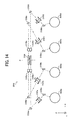
- FIG. 14 is a side view of the optical scanning device shown in FIG. 12 ;
- FIG. 15 is a schematic diagram of a displacement detector shown in FIG. 12 ;
- FIG. 16 is a schematic diagram for explaining toner patches for displacement detection.
- FIG. 1 is a schematic diagram of a laser printer 1000 as an image forming apparatus according to an embodiment of the present invention.
- the laser printer 1000 includes an optical scanning device 1010 , a photosensitive drum 1030 , an electrostatic charger 1031 , a developing roller 1032 , a transfer charger 1033 , a neutralizing unit 1034 , a cleaning blade 1035 , a toner cartridge 1036 , a sheet feeding roller 1037 , a sheet feeding tray 1038 , a pair of registration rollers 1039 , a fixing roller 1041 , discharge rollers 1042 , a discharge tray 1043 , a communication controller 1050 , and a printer controller 1060 that integrally controls the above units.
- the units are placed at a predetermined position inside a printer body 1044 .
- the communication controller 1050 controls a two-way communication with external devices via a network etc.
- the photosensitive drum 1030 is a cylindrical member and a photosensitive layer is formed on a surface of the photosensitive drum 1030 .
- the surface of the photosensitive drum 1030 is a target surface to be scanned.
- the photosensitive drum 1030 rotates in a direction indicated by an arrow shown in FIG. 1 .
- the electrostatic charger 1031 , the developing roller 1032 , the transfer charger 1033 , the neutralizing unit 1034 , and the cleaning blade 1035 are sequentially disposed in that order along the surface of the photosensitive drum 1030 along a rotation direction of the photosensitive drum 1030 .
- the electrostatic charger 1031 uniformly charges the surface of the photosensitive drum 1030 .
- the optical scanning device 1010 irradiates light beams, which are modulated based on image data from a higher-level device (for example, a personal computer), on the surface of the photosensitive drum 1030 that is charged by the electrostatic charger 1031 . Due to this, a latent image corresponding to the image data is formed on the surface of the photosensitive drum 1030 . The latent image moves in a direction of the developing roller 1032 with a rotation of the photosensitive drum 1030 . A structure of the optical scanning device 1010 will be described later.
- the toner cartridge 1036 stores therein toner and the toners are supplied to the developing roller 1032 .
- the developing roller 1032 causes the toner supplied from the toner cartridge 1036 to adhere to the latent image formed on the surface of the photosensitive drum 1030 , and converts the image data into a visual image.
- the latent image (hereinafter, “toner image”) to which the toner is deposited moves towards the transfer charger 1033 with the rotation of the photosensitive drum 1030 .
- the sheet feeding tray 1038 stores therein recording sheets 1040 .
- the sheet feeding roller 1037 is disposed in the vicinity of the sheet feeding tray 1038 .
- the sheet feeding roller 1037 picks up the recording sheets 1040 one by one from the sheet feeding tray 1038 and conveys to the pair of the registration rollers 1039 .
- the registration rollers 1039 temporarily hold the recording sheets 1040 picked up by the sheet feeding roller 1037 , and transmit, along with the rotation of the photosensitive drum 1030 , the recording sheets 1040 towards a gap between the photosensitive drum 1030 and the transfer charger 1033 .
- a voltage of opposite polarity is applied to the transfer charger 1033 . Due to the voltage, a toner image on the surface of the photosensitive drum 1030 is transferred to the recording sheets 1040 .
- the recording sheets 1040 to which the toner images are transferred are delivered to the fixing roller 1041 .
- Heat and pressure are applied to the recording sheets 1040 at the fixing roller 1041 and thus the toner is fixed on the recording sheets 1040 .
- the recording sheets 1040 on which the toner is fixed are transferred to the discharge tray 1043 via the discharge rollers 1042 and sequentially stacked in the discharge tray 1043 .
- the neutralizing unit 1034 neutralizes the electric charge of the surface of the photosensitive drum 1030 .
- the cleaning blade 1035 removes the toner (residual toner) remaining on the surface of the photosensitive drum 1030 . Further, the removed residual toner is reutilized. The surface of the photosensitive drum 1030 on which the electric charge is neutralized again returns to a position of the electrostatic charger 1031 .
- optical scanning device 1010 The structure of the optical scanning device 1010 is explained below.
- the optical scanning device 1010 includes a light source 14 , a coupling lens 15 , an aperture plate 16 , a cylindrical lens 17 , a polygon mirror 13 , a deflector-side scanning lens 11 a , an image-surface-side scanning lens 11 b , two light detecting sensors 18 a and 18 b , two light detecting mirrors 19 a and 19 b , and a scanning controller 22 (omitted in FIG. 2 , shown in FIG. 4 ). These components of the optical scanning device 1010 are assembled at a predetermined position inside a housing 21 .
- a three-dimensional orthogonal coordinate system is used, and a direction along a longitudinal direction of the photosensitive drum 1030 is assumed as a Y-axis direction and a direction along an optical axis of both the deflector-side scanning lens 11 a and the image-surface-side scanning lens 11 b is assumed as an X-axis direction.
- the light source 14 includes a two-dimensional array 100 formed of 12 light-emitting units (v 1 to v 12 ) arranged in a matrix form on a base plate. Further, light beams emitted from the light emitting units v 1 to v 12 are indicated by CH 1 to CH 12 , respectively.
- a direction M shown in FIG. 3 corresponds to the main scanning direction and a direction S corresponds to a sub-scanning direction (in the example shown in FIG. 3 , same as a Z-axis direction). Further, a direction T is a direction that makes an angle of inclination ⁇ (0° ⁇ 90°) from the direction M towards the direction S.
- Each of the light emitting units v 1 to v 12 is a vertical cavity surface emitting laser (VCSEL) having an emission wavelength of 780 nanometers.
- VCSEL vertical cavity surface emitting laser
- the coupling lens 15 collimates the light beam emitted from the light source 14 .
- the aperture plate 16 includes an aperture and defines a diameter of the light beam coming from the coupling lens 15 .
- the cylindrical lens 17 forms an image of the light beam, which passes through the aperture of the aperture plate 16 , in the vicinity of a deflecting-reflecting surface of the polygon mirror 13 , in a direction corresponding to the sub-scanning direction (in the example shown in FIG. 2 , Z-axis direction).
- An optical system disposed on an optical path between the light source 14 and the polygon mirror 13 is also referred to as a pre-deflector optical system.
- the pre-deflector optical system according to the present embodiment includes the coupling lens 15 , the aperture plate 16 , and the cylindrical lens 17 .
- the polygon mirror 13 includes mirrors on four surfaces and each mirror functions as the deflecting-reflecting surface.
- the polygon mirror 13 rotates at a constant speed around an axis parallel to the direction (in the example shown in FIG. 2 , Z-axis direction) corresponding to the sub-scanning direction, and deflects the light beam coming from the cylindrical lens 17 .
- the deflector-side scanning lens 11 a is disposed on the optical path of the light beam deflected by the polygon mirror 13 .
- the image-surface-side scanning lens 11 b is disposed on the optical path of the light beam coming from the deflector-side scanning lens 11 a .
- the light beam that has passed through the image-surface-side scanning lens 11 b is irradiated on the surface of the photosensitive drum 1030 and an optical spot is formed.
- the optical spot moves in a longitudinal direction of the photosensitive drum 1030 with the rotation of the polygon mirror 13 . In other words, the photosensitive drum 1030 is scanned.
- a movement direction of the optical spot corresponds to the main scanning direction.
- the optical system disposed on the optical path between the polygon mirror 13 and the photosensitive drum 1030 is also referred to as a scanning optical system.
- the scanning optical system according to the present embodiment includes the deflector-side scanning lens 11 a and the image-surface-side scanning lens 11 b.
- Each of the light detecting sensor 18 a and 18 b includes a plurality of light receiving elements or a plurality of light receiving regions corresponding to a plurality of the light emitting units. Each light receiving element or each light receiving region respectively generates photoelectric conversion signals and outputs the signals to the scanning controller 22 .
- the scanning controller 22 includes a CPU 210 , a flash memory 211 , a RAM 212 , an interface (I/F) 214 , a pixel-clock generating circuit 215 , an image processing circuit 216 , a frame memory 217 , line buffers 218 1 to 218 12 , a writing control circuit 219 , and a light-source drive circuit 221 .
- Arrows shown in FIG. 4 indicate a flow of typical signals and data, and do not express all connection relations of each clock.
- the pixel-clock generating circuit 215 generates pixel clock signals.
- the frame memory 217 temporarily stores therein raster-expanded image data (hereinafter, “raster data”).
- the image processing circuit 216 reads the raster data stored in the frame memory 217 and generates, upon carrying out a predetermined halftone process, a dot data for each of the light emitting units v 1 to v 12 , and outputs the dot data to the line buffers 218 1 to 218 12 corresponding to the light emitting units v 1 to v 12 , respectively.
- the writing control circuit 219 calculates a scanning start timing.
- the writing control circuit 219 reads the dot data of each of the light emitting units v 1 to v 12 from the line buffers 218 1 to 218 12 in synchronization with the scanning start time and generates independent modulation data for each of the light emitting units v 1 to v 12 along with superimposing to the pixel clock signals from the pixel-clock generating circuit 215 .
- the light source drive circuit 221 drives each of the light emitting units v 1 to v 12 of the two-dimensional array 100 depending on the modulation data from the writing control circuit 219 .
- the flash memory 211 stores therein various computer programs described by program codes decodable by the CPU 210 and various data used for executing various computer programs.
- the RAM 212 is a work memory.
- the CPU 210 operates according to the computer programs stored in the flash memory 211 and controls the entire optical scanning device 1010 .
- the I/F 214 is a communication I/F that controls the two-way communication with the printer controller 1060 . Image data from the higher-level device is received via the I/F 214 .
- a position of the optical spot on the surface of the photosensitive drum 1030 is displaced in the main scanning direction with respect to a desired position of the optical spot.
- a position P 1 shown in FIG. 5 indicates a drawing start position of a drawing area (effective scan area) and a position P 2 indicates a drawing end position of the drawing area.
- a symbol ⁇ Pm shown in FIG. 5 indicates a magnitude of variation of the displacement amount (hereinafter, “main-scanning displacement amount”) of the optical spots in the main scanning direction of all the light beams CH (CH 1 to CH 12 ).
- an image brightness (L*) increases when printed on the sheet.
- the image brightness (L*) increases in a straight line from the drawing start position P 1 towards the drawing end position P 2 as shown in FIG. 7B .
- the brightness difference is equal to or larger than 5 levels, the density difference between one end of the sheet and the other end of the sheet can be apparently seen as shown in FIG. 7C .
- the CPU 210 When carrying out an image data writing process on the photosensitive drum 1030 , if the brightness difference may become equal to or larger than 5 levels, the CPU 210 carries out a brightness-difference correction process such that the brightness difference is not apparently seen.
- the brightness-difference correction process executed by the CPU 210 is explained below. It is assumed that a relation between “ ⁇ Pm” and “ ⁇ Pw” that is a light-emitting power correction amount required for controlling a change of the image brightness (L*) (see FIG. 8 ) is calculated in advance by experiments, simulations, theoretical calculations etc. and stored in the flash memory 211 .
- the main-scanning displacement amount at the drawing end position P 2 is calculated for each light emitting unit.
- the light-source drive circuit 221 is instructed to change the light emitting power from Pw 1 to Pw 2 to be almost in a straight line from the drawing start position P 1 towards the drawing end position P 2 (see FIG. 9 ). In other words, the light emitting power is modulated and a writing energy density is corrected.
- the writing energy density on the surface of the photosensitive drum 1030 changes almost in a straight line from the drawing start position P 1 towards the drawing end position P 2 .
- the image brightness (L*) becomes almost uniform when printed on the sheet, and as shown in FIG. 10C , little density difference is seen between one end of the sheet and the other end of the sheet.
- a correcting device includes the scanning controller 22 .
- the processes performed by the computer programs executed by the CPU 210 can be realized at least partly or entirely by using hardware.
- a write method according to the present embodiment is executed in the brightness-difference correction process mentioned above.
- the scanning controller 22 instructs the light-source drive circuit 221 to change the light emitting power from Pw 1 to Pw 2 to be almost in a straight line from the drawing start position P 1 towards the drawing end position P 2 .
- the writing energy density on the surface of the photosensitive drum 1030 changes along a substantial straight line from the drawing start position P 1 to the drawing end position P 2 .
- the image brightness (L*) becomes almost uniform and little density difference is seen between one end of the sheet and the other end of the sheet.
- the desired latent image can be formed on the surface of the photosensitive drum 1030 without increasing costs.
- the laser printer 1000 includes the optical scanning device 1010 that can form a desired latent image on the surface of the photosensitive drum 1030 without increasing costs. Thus, a high quality image can be formed at a low cost.
- the writing energy density is corrected by modulating the light emitting power as explained in the embodiment, the present invention is not to be thus limited.
- the writing energy density can be corrected by modulating a pulse width.
- the writing energy density is corrected such that the writing energy density changes almost in a straight line from the drawing start position P 1 towards the drawing end position P 2 as explained above, the writing energy density can be corrected such that the writing energy density changes in a stepped manner.
- the writing energy density can also be partially changed.
- a unidimensional array having a plurality of the light emitting units unidimensionally arranged can be used in place of the two-dimensional array 100 .
- the image forming apparatus is not limited to the laser printer 1000 . As long as the image forming apparatus includes the optical scanning device 1010 , high quality images can be formed without increasing costs.
- the image forming apparatus can be one that irradiates laser beams directly on a medium (for example, a sheet) capable of being colored with the laser beams.
- a medium for example, a sheet
- the image forming apparatus that uses a silver film as an image carrying member can be used.
- the latent image is formed on the silver film by optical scanning and the latent image can be visualized by a process equivalent to a developing process in normal silver halide photography.
- the latent image can be transferred to a photographic printing paper by a process equivalent to a printing process in the normal silver halide photography.
- Such an image forming apparatus can be executed as an optical printing device and as an optical drawing device that takes computer tomography (CT) scan images etc.
- CT computer tomography
- high quality images can be formed at a high speed by using the optical scanning device that supports color images.
- a printer 2000 that supports color images and includes a plurality of the photosensitive drums can also be used.
- the printer 2000 is a tandem-type multicolor printer that forms full color images by superimposing four colors (black, cyan, magenta, and yellow) one on top of the other.
- the printer 2000 includes an optical scanning device 2010 , four photosensitive drums 2030 a , 2030 b , 2030 c , and 2030 d , four electrostatic chargers 2032 a , 2032 b , 2032 c , and 2032 d , four developing rollers 2033 a , 2033 b , 2033 c , and 2033 d , four toner cartridges 2034 a , 2034 b , 2034 c , and 2034 d , four cleaning cases 2031 a , 2031 b , 2031 c , and 2031 d , a transfer belt 2040 , a sheet feeding tray 2060 , a sheet feeding roller 2054 , a pair of registration rollers 2056 , a fixing roller 2050 , a discharge tray 2070 , discharge rollers
- the optical scanning device 2010 includes two light source units 2200 a and 2200 b , two aperture plates 2201 a and 2201 b , two light-beam splitting prisms 2202 a and 2202 b , a polygon mirror 2104 , four liquid-crystal deflecting elements 2203 a , 2203 b , 2203 c , and 2203 d , four cylindrical lenses 2204 a , 2204 b , 2204 c , and 2204 d , four f ⁇ lenses 2105 a , 2105 b , 2105 c , and 2105 d , eight reflecting mirrors 2106 a , 2106 b , 2106 c , 2106 d , 2108 a , 2108 b , 2108 c , and 2108 d , four toroidal lenses 2107 a , 2107 b , 2107 c , and 2107 d , four synchronization
- the photosensitive drum 2030 a , the electrostatic charger 2032 a , the developing roller 2033 a , the toner cartridge 2034 a , the cleaning case 2031 a , the liquid-crystal deflecting element 2203 a , the cylindrical lens 2204 a , the f ⁇ lens 2105 a , the reflecting mirror 2106 a , the toroidal lens 2107 a , the reflecting mirror 2108 a , and the synchronization detecting sensor 2205 a are used in combination, and constitute an image forming station (hereinafter, “K station”) that forms a black image.
- K station image forming station
- the photosensitive drum 2030 b , the electrostatic charger 2032 b , the developing roller 2033 b , the toner cartridge 2034 b , the cleaning case 2031 b , the liquid-crystal deflecting element 2203 b , the cylindrical lens 2204 b , the f ⁇ lens 2105 b , the reflecting mirror 2106 b , the toroidal lens 2107 b , the reflecting mirror 2108 b , and the synchronization detecting sensor 2205 b are used in combination, and constitute an image forming station (hereinafter, “C station”) that forms a cyan image.
- C station image forming station
- M station image forming station
- the photosensitive drum 2030 d , the electrostatic charger 2032 d , the developing roller 2033 d , the toner cartridge 2034 d , the cleaning case 2031 d , the liquid-crystal deflecting element 2203 d , the cylindrical lens 2204 d , the f ⁇ lens 2105 d , the reflecting mirror 2106 d , the toroidal lens 2107 d , the reflecting mirror 2108 d , and the synchronization detecting sensor 2205 d are used in combination, and constitute an image forming station (hereinafter, “Y station”) that forms a yellow image.
- Y station image forming station
- Each of the light source units 2200 a and 2200 b includes the two-dimensional array 100 .
- the light beam which is emitted from the light source unit 2200 a and passing through the aperture of the aperture plate 2201 a , is split into a light beam for the K station and a light beam for the C station by the light-beam splitting prism 2202 a . Further, the light beam, which is emitted from the light source unit 2200 b and passing through the aperture of the aperture plate 2201 b , is split into a light beam for the M station and a light beam for the Y station by the light-beam splitting prism 2202 b.
- the light beam for the K station passes through the liquid-crystal deflecting element 2203 a and the cylindrical lens 2204 a , and is deflected by the polygon mirror 2104 . Subsequently, the light beam passes through the f ⁇ lens 2105 a , the reflecting mirror 2106 a , the toroidal lens 2107 a , and the reflecting mirror 2108 a , and is focused on a surface of the photosensitive drum 2030 a.
- the light beam for the C station passes through the liquid-crystal deflecting element 2203 b and the cylindrical lens 2204 b , and is deflected by the polygon mirror 2104 . Subsequently, the light beam passes through the fO lens 2105 b , the reflecting mirror 2106 b , the toroidal lens 2107 b , and the reflecting mirror 2108 b , and is focused on a surface of the photosensitive drum 2030 b.
- the light beam for the M station passes through the liquid-crystal deflecting element 2203 c and the cylindrical lens 2204 c , and is deflected by the polygon mirror 2104 . Subsequently, the light beam passes through the fO lens 2105 c , the reflecting mirror 2106 c , the toroidal lens 2107 c , and the reflecting mirror 2108 c , and is focused on a surface of the photosensitive drum 2030 c.
- the light beam for the Y station passes through the liquid-crystal deflecting element 2203 d and the cylindrical lens 2204 d , and is deflected by the polygon mirror 2104 . Subsequently, the light beam passes through the f ⁇ lens 2105 d , the reflecting mirror 2106 d , the toroidal lens 2107 d , and the reflecting mirror 2108 d , and is focused on a surface of the photosensitive drum 2030 d.
- Each of the synchronization detecting sensors 2205 a to 2205 d is similar to the light detecting sensor 18 a and used for detecting start of main scanning in the corresponding photosensitive drum.
- the displacement detector 2045 is disposed on ⁇ X side of the transfer belt 2040 .
- the displacement detector 2045 includes an LED 2042 a , a photosensor 2041 a , an LED 2042 b , a photosensor 2041 b , an LED 2042 c , and a photosensor 2041 c .
- the LED 2042 a illuminates a +Y side end (assumed as a detection position 0) of the transfer belt 2040 .
- the photosensor 2041 a receives a reflected light from the LED 2042 a .
- the LED 2042 b illuminates a central portion (assumed as a detection position 1) of the transfer belt 2040 .
- the photosensor 2041 b receives the reflected light from the LED 2042 b
- the LED 2042 c illuminates a ⁇ Y side end (assumed as a detection position 2) of the transfer belt 2040 .
- the photosensor 2041 c receives the reflected light from the LED 2042 c.
- the displacement detector 2045 illuminates detection patterns (toner patches) Pk, which are formed at each detection position, using the respective LEDs, receives the reflected light using each photosensor, and thus outputs a plurality of signals that include displacement data in the main scanning direction.
- each detection pattern Pk is formed of a first set of lines that is arranged such that a longitudinal direction is parallel to the main scanning direction and a second set of lines that is arranged such that a longitudinal direction is inclined at 45° with respect to the main scanning direction.
- the scanning controller calculates, from the output signals of the displacement detector 2045 , the main-scanning displacement amount for each scanning line on the photosensitive drum (for example, see Japanese Patent No. 3644923). For example, when the brightness difference may be equal to or larger than 5 levels, the scanning controller corrects, similar to the scanning controller 22 , the writing energy density by modulating the light emitting power for each photosensitive drum.
- the scanning controller can be set for each color or for each pair of two colors.
- a correcting device corrects a writing energy density, which is an amount of light per unit surface area of a target surface to be scanned, with respect to a write position based on a displacement amount in a main scanning direction of each of a plurality of light beams focused on the target surface such that a density change of an image due to a variation of the displacement amount is reduced. Consequently, a desired image can be formed on the target surface without increasing costs.
- the writing energy density is corrected with respect to the write position such that the density change of the image due to the variation of the displacement amount is reduced. Consequently, the desired image can be formed on the exposed scan surface without increasing costs.
- At least one optical scanning device according to the present invention can be provided in an image forming apparatus, a high quality image can be formed without increasing costs.
Abstract
Description
Claims (11)
Applications Claiming Priority (2)
| Application Number | Priority Date | Filing Date | Title |
|---|---|---|---|
| JP2007-235292 | 2007-09-11 | ||
| JP2007235292A JP2009066803A (en) | 2007-09-11 | 2007-09-11 | Optical scanner, writing method, and image formation device |
Publications (2)
| Publication Number | Publication Date |
|---|---|
| US20090074437A1 US20090074437A1 (en) | 2009-03-19 |
| US8072478B2 true US8072478B2 (en) | 2011-12-06 |
Family
ID=40454589
Family Applications (1)
| Application Number | Title | Priority Date | Filing Date |
|---|---|---|---|
| US12/207,047 Expired - Fee Related US8072478B2 (en) | 2007-09-11 | 2008-09-09 | Optical scanning device, image forming apparatus, and write method |
Country Status (2)
| Country | Link |
|---|---|
| US (1) | US8072478B2 (en) |
| JP (1) | JP2009066803A (en) |
Cited By (2)
| Publication number | Priority date | Publication date | Assignee | Title |
|---|---|---|---|---|
| US8675034B2 (en) | 2011-01-06 | 2014-03-18 | Ricoh Company, Limited | Optical scanning apparatus and image forming apparatus |
| US8896649B2 (en) | 2011-01-17 | 2014-11-25 | Ricoh Company, Limited | Optical scanning device and image forming apparatus |
Families Citing this family (21)
| Publication number | Priority date | Publication date | Assignee | Title |
|---|---|---|---|---|
| JP5531458B2 (en) * | 2008-08-01 | 2014-06-25 | 株式会社リコー | Speed detection device and multicolor image forming apparatus |
| US8237760B2 (en) * | 2008-08-19 | 2012-08-07 | Ricoh Company, Ltd. | Light-source driving device, optical scanning device, and counting method |
| JP5381371B2 (en) * | 2008-11-07 | 2014-01-08 | 株式会社リコー | Polarization separation device, optical scanning device, and image forming apparatus |
| JP5333070B2 (en) * | 2009-06-15 | 2013-11-06 | 株式会社リコー | Optical scanning apparatus and image forming apparatus |
| JP4825295B2 (en) * | 2009-10-21 | 2011-11-30 | 日高精機株式会社 | Processing oil application equipment |
| JP5568958B2 (en) | 2009-11-02 | 2014-08-13 | 株式会社リコー | Exposure apparatus and image forming apparatus |
| JP5505617B2 (en) * | 2009-12-10 | 2014-05-28 | 株式会社リコー | Optical scanning apparatus and image forming apparatus |
| JP2011159943A (en) * | 2010-01-08 | 2011-08-18 | Ricoh Co Ltd | Surface emitting laser element, surface emitting laser array, optical scanner device, and image forming apparatus |
| JP5407880B2 (en) * | 2010-01-13 | 2014-02-05 | 株式会社リコー | Optical scanning apparatus and image forming apparatus |
| JP5691633B2 (en) | 2010-06-25 | 2015-04-01 | 株式会社リコー | Optical scanning apparatus and image forming apparatus |
| JP2012025130A (en) | 2010-07-27 | 2012-02-09 | Ricoh Co Ltd | Image forming apparatus |
| JP2012058465A (en) | 2010-09-08 | 2012-03-22 | Ricoh Co Ltd | Optical scanning device and picture formation device |
| JP5679110B2 (en) | 2011-01-25 | 2015-03-04 | 株式会社リコー | Image forming apparatus |
| US8654168B2 (en) | 2011-08-03 | 2014-02-18 | Ricoh Company, Ltd. | Optical scanning device, image forming apparatus, and optical scanning device designing method |
| JP5903894B2 (en) | 2012-01-06 | 2016-04-13 | 株式会社リコー | Optical scanning apparatus and image forming apparatus |
| JP5942493B2 (en) | 2012-03-12 | 2016-06-29 | 株式会社リコー | Optical scanning apparatus and image forming apparatus |
| JP6024212B2 (en) | 2012-05-31 | 2016-11-09 | 株式会社リコー | Method for manufacturing image forming apparatus, method for adjusting light amount of print head, and method for manufacturing process cartridge |
| JP5962909B2 (en) | 2012-07-20 | 2016-08-03 | 株式会社リコー | Imaging optical system, print head, image forming apparatus, and image reading apparatus |
| JP6108160B2 (en) | 2013-03-13 | 2017-04-05 | 株式会社リコー | Imaging optical system, printer head, and image forming apparatus |
| JP6287246B2 (en) | 2014-01-21 | 2018-03-07 | 株式会社リコー | Printhead manufacturing method, printhead, and image forming apparatus |
| JP6657897B2 (en) | 2015-12-10 | 2020-03-04 | 株式会社リコー | Mirror member processing method |
Citations (51)
| Publication number | Priority date | Publication date | Assignee | Title |
|---|---|---|---|---|
| US6233081B1 (en) | 1998-12-24 | 2001-05-15 | Ricoh Company Ltd. | Optical scanning device, image forming apparatus and optical scanning method |
| US6347004B1 (en) | 1998-08-31 | 2002-02-12 | Ricoh Company, Ltd. | Optical scanning apparatus and scanning image forming lens |
| US6384949B1 (en) | 1999-02-25 | 2002-05-07 | Ricoh Company Ltd. | Optical scanning device, image forming apparatus and optical scanning method |
| US6388792B1 (en) | 1999-07-09 | 2002-05-14 | Ricoh Company, Ltd. | Optical scanning device and image forming apparatus |
| US6400391B1 (en) | 1999-06-09 | 2002-06-04 | Ricoh Company, Ltd. | Optical scanning lens, optical scanning device and image forming apparatus |
| US6417509B1 (en) | 1999-03-23 | 2002-07-09 | Ricoh Technology Research, Inc. | Optical scanning apparatus and image forming apparatus |
| US20020114081A1 (en) * | 2001-02-19 | 2002-08-22 | Nec Corporation | Laser scanning optics and laser scanning method using the same |
| US6448998B1 (en) | 1999-08-31 | 2002-09-10 | Ricoh Company, Ltd. | Scanning and imaging lens, optical scanning device and image forming apparatus |
| US6509995B1 (en) | 1999-09-01 | 2003-01-21 | Ricoh Company, Ltd. | Optical scanning device, line-image forming optical system therein, imaging adjustment method in the device and image forming apparatus |
| US6596985B2 (en) | 2000-02-22 | 2003-07-22 | Rioch Company, Ltd. | Multi-beam scanning device, multi-beam scanning method, light source device, and image forming apparatus |
| US6657761B2 (en) | 2000-03-27 | 2003-12-02 | Ricoh Company, Ltd. | Optical scanning device, image forming apparatus, and optical scanning method |
| US20040036936A1 (en) | 2002-07-02 | 2004-02-26 | Tomohiro Nakajima | Optical scanner and image forming apparatus |
| US6771407B2 (en) | 2001-09-20 | 2004-08-03 | Ricoh Company, Ltd. | Optical scanner and image formation apparatus |
| US6781729B2 (en) | 2001-07-30 | 2004-08-24 | Ricoh Company, Ltd. | Optical scanning system with unvarying image surface under environmental temperature change |
| US6785028B1 (en) | 1999-11-24 | 2004-08-31 | Ricoh Company, Ltd. | Optical scanning device having a temperature compensation unit |
| US6788444B2 (en) | 2001-10-24 | 2004-09-07 | Ricoh Company, Ltd. | Method and apparatus for optical scanning capable of reducing a dot position displacement and a dot diameter variation |
| US6791729B2 (en) | 2001-06-05 | 2004-09-14 | Ricoh Company, Ltd. | Adjusting imaging position of optical beam spot in main and sub-scanning directions by individually and/or collectively adjusting position(s) of temperature-compensating lens(es) |
| US6813051B2 (en) | 2003-02-17 | 2004-11-02 | Ricoh Company, Ltd. | Optical scanner and image forming apparatus |
| US20040240000A1 (en) | 2003-05-29 | 2004-12-02 | Naoki Miyatake | Optical scanning device and image forming apparatus |
| US6829104B2 (en) | 2001-06-05 | 2004-12-07 | Ricoh Company, Ltd. | Resin-made non-spherical optical element, optical scanning device using the optical element, and image forming apparatus using the optical scanning device |
| US6833940B2 (en) | 2001-10-24 | 2004-12-21 | Ricoh Company, Ltd. | Method and apparatus for optical scanning capable of performing a high speed and high pixel density scanning |
| US20050024479A1 (en) | 2003-05-07 | 2005-02-03 | Akihisa Itabashi | Optical scanning apparatus, image forming apparatus, and beam positioning method |
| US6906739B2 (en) | 2002-03-01 | 2005-06-14 | Ricoh Company, Ltd. | Optical scanner and imaging apparatus using the same |
| US20050190420A1 (en) | 2004-02-18 | 2005-09-01 | Shigeaki Imai | Beam-spot position compensation method, optical scanning device, and multi-color image forming device |
| US6999208B2 (en) | 2000-09-22 | 2006-02-14 | Ricoh Company, Ltd. | Optical scanner, optical scanning method, scanning image forming optical system, optical scanning lens and image forming apparatus |
| US7006120B2 (en) | 2002-08-07 | 2006-02-28 | Ricoh Company, Ltd. | Multi-beam optical scanning apparatus and image forming apparatus |
| US7038822B2 (en) | 2002-05-22 | 2006-05-02 | Ricoh Company, Ltd. | Optical element, optical scanner and image forming apparatus |
| US7045773B2 (en) | 2003-07-18 | 2006-05-16 | Ricoh Company, Ltd. | Optical scanning apparatus for accurately detecting and correcting position of optical beam in subscanning direction, and the method |
| US7050082B2 (en) | 2002-01-23 | 2006-05-23 | Ricoh Company, Ltd. | Image forming system employing effective optical scan-line control device |
| US7061658B2 (en) | 2001-01-18 | 2006-06-13 | Ricoh Company, Ltd. | Scanning image formation optical system, optical scanner using the optical system, and image forming apparatus using the optical scanner |
| US20060158711A1 (en) | 2004-12-22 | 2006-07-20 | Shigeaki Imai | Image forming device and image forming method |
| US7088485B2 (en) | 2002-12-27 | 2006-08-08 | Ricoh Company, Ltd. | Optical scanner and image formation apparatus |
| US7167288B2 (en) | 2003-11-05 | 2007-01-23 | Ricoh Company, Ltd. | Optical scanning unit, image forming apparatus, and method of correcting positional misalignment |
| US20070058255A1 (en) | 2005-09-09 | 2007-03-15 | Shigeaki Imai | Optical scanner and image forming apparatus |
| US7215354B1 (en) | 1999-10-05 | 2007-05-08 | Ricoh Company, Ltd. | Scanning optical system, optical scanning device and image forming apparatus |
| JP2007130793A (en) | 2005-11-08 | 2007-05-31 | Ricoh Co Ltd | Pixel clock generation device, pulse modulation device, and image forming apparatus |
| US20070132828A1 (en) | 2005-12-09 | 2007-06-14 | Masaaki Ishida | Optical scanner and image forming apparatus |
| US7256815B2 (en) | 2001-12-20 | 2007-08-14 | Ricoh Company, Ltd. | Image forming method, image forming apparatus, optical scan device, and image forming apparatus using the same |
| US7277212B2 (en) | 2003-09-19 | 2007-10-02 | Ricoh Company, Limited | Optical scanning unit and image forming apparatus |
| US20070236557A1 (en) | 2005-12-21 | 2007-10-11 | Shigeaki Imai | Laser beam scanning device, image forming apparatus, and laser beam detecting method by the laser beam scanning device |
| US20080019255A1 (en) | 2006-07-21 | 2008-01-24 | Shigeaki Imai | Light source unit, phase type optical element, and laser beam scanning device |
| US7333254B2 (en) | 2002-03-15 | 2008-02-19 | Ricoh Company, Ltd. | Optical scanning apparatus, illuminant apparatus and image forming apparatus |
| US20080068678A1 (en) | 2006-09-15 | 2008-03-20 | Mitsuo Suzuki | Optical scanning apparatus and image forming apparatus |
| US20080088893A1 (en) * | 2006-08-04 | 2008-04-17 | Masaaki Ishida | Optical scanning device, optical scanning method, computer program product for executing optical scanning method, recording medium with computer program recorded thereon, image forming apparatus, and color image forming apparatus using the same |
| US20080123160A1 (en) * | 2006-10-27 | 2008-05-29 | Atsufumi Omori | Optical scanning device having a plurality of light sources, optical scanning method, pixel forming device, image forming apparatus using the optical scanning device having a plurality of light sources, and color image forming apparatus using the same |
| US20080170283A1 (en) | 2007-01-17 | 2008-07-17 | Shigeaki Imai | Optical scanner and image forming apparatus |
| US7403316B2 (en) | 2004-01-14 | 2008-07-22 | Ricoh Company, Ltd. | Optical scanning device, image forming apparatus and liquid crystal device driving method |
| US20080192323A1 (en) | 2007-02-13 | 2008-08-14 | Tadashi Nakamura | Optical scanning device and image forming apparatus |
| US20080204852A1 (en) | 2006-02-27 | 2008-08-28 | Taku Amada | Optical scanning apparatus, an image formation apparatus, and a phase modulation method |
| US20080204841A1 (en) | 2007-02-22 | 2008-08-28 | Seizo Suzuki | Optical scanning device and image forming apparatus |
| US20080225106A1 (en) | 2007-03-02 | 2008-09-18 | Atsufumi Omori | Light-source driving device, optical scanning device, and image forming apparatus |
-
2007
- 2007-09-11 JP JP2007235292A patent/JP2009066803A/en active Pending
-
2008
- 2008-09-09 US US12/207,047 patent/US8072478B2/en not_active Expired - Fee Related
Patent Citations (51)
| Publication number | Priority date | Publication date | Assignee | Title |
|---|---|---|---|---|
| US6347004B1 (en) | 1998-08-31 | 2002-02-12 | Ricoh Company, Ltd. | Optical scanning apparatus and scanning image forming lens |
| US6233081B1 (en) | 1998-12-24 | 2001-05-15 | Ricoh Company Ltd. | Optical scanning device, image forming apparatus and optical scanning method |
| US6384949B1 (en) | 1999-02-25 | 2002-05-07 | Ricoh Company Ltd. | Optical scanning device, image forming apparatus and optical scanning method |
| US6417509B1 (en) | 1999-03-23 | 2002-07-09 | Ricoh Technology Research, Inc. | Optical scanning apparatus and image forming apparatus |
| US6400391B1 (en) | 1999-06-09 | 2002-06-04 | Ricoh Company, Ltd. | Optical scanning lens, optical scanning device and image forming apparatus |
| US6388792B1 (en) | 1999-07-09 | 2002-05-14 | Ricoh Company, Ltd. | Optical scanning device and image forming apparatus |
| US6448998B1 (en) | 1999-08-31 | 2002-09-10 | Ricoh Company, Ltd. | Scanning and imaging lens, optical scanning device and image forming apparatus |
| US6509995B1 (en) | 1999-09-01 | 2003-01-21 | Ricoh Company, Ltd. | Optical scanning device, line-image forming optical system therein, imaging adjustment method in the device and image forming apparatus |
| US7215354B1 (en) | 1999-10-05 | 2007-05-08 | Ricoh Company, Ltd. | Scanning optical system, optical scanning device and image forming apparatus |
| US6785028B1 (en) | 1999-11-24 | 2004-08-31 | Ricoh Company, Ltd. | Optical scanning device having a temperature compensation unit |
| US6596985B2 (en) | 2000-02-22 | 2003-07-22 | Rioch Company, Ltd. | Multi-beam scanning device, multi-beam scanning method, light source device, and image forming apparatus |
| US6657761B2 (en) | 2000-03-27 | 2003-12-02 | Ricoh Company, Ltd. | Optical scanning device, image forming apparatus, and optical scanning method |
| US6999208B2 (en) | 2000-09-22 | 2006-02-14 | Ricoh Company, Ltd. | Optical scanner, optical scanning method, scanning image forming optical system, optical scanning lens and image forming apparatus |
| US7061658B2 (en) | 2001-01-18 | 2006-06-13 | Ricoh Company, Ltd. | Scanning image formation optical system, optical scanner using the optical system, and image forming apparatus using the optical scanner |
| US20020114081A1 (en) * | 2001-02-19 | 2002-08-22 | Nec Corporation | Laser scanning optics and laser scanning method using the same |
| US6829104B2 (en) | 2001-06-05 | 2004-12-07 | Ricoh Company, Ltd. | Resin-made non-spherical optical element, optical scanning device using the optical element, and image forming apparatus using the optical scanning device |
| US6791729B2 (en) | 2001-06-05 | 2004-09-14 | Ricoh Company, Ltd. | Adjusting imaging position of optical beam spot in main and sub-scanning directions by individually and/or collectively adjusting position(s) of temperature-compensating lens(es) |
| US6781729B2 (en) | 2001-07-30 | 2004-08-24 | Ricoh Company, Ltd. | Optical scanning system with unvarying image surface under environmental temperature change |
| US6771407B2 (en) | 2001-09-20 | 2004-08-03 | Ricoh Company, Ltd. | Optical scanner and image formation apparatus |
| US6833940B2 (en) | 2001-10-24 | 2004-12-21 | Ricoh Company, Ltd. | Method and apparatus for optical scanning capable of performing a high speed and high pixel density scanning |
| US6788444B2 (en) | 2001-10-24 | 2004-09-07 | Ricoh Company, Ltd. | Method and apparatus for optical scanning capable of reducing a dot position displacement and a dot diameter variation |
| US7256815B2 (en) | 2001-12-20 | 2007-08-14 | Ricoh Company, Ltd. | Image forming method, image forming apparatus, optical scan device, and image forming apparatus using the same |
| US7050082B2 (en) | 2002-01-23 | 2006-05-23 | Ricoh Company, Ltd. | Image forming system employing effective optical scan-line control device |
| US6906739B2 (en) | 2002-03-01 | 2005-06-14 | Ricoh Company, Ltd. | Optical scanner and imaging apparatus using the same |
| US7333254B2 (en) | 2002-03-15 | 2008-02-19 | Ricoh Company, Ltd. | Optical scanning apparatus, illuminant apparatus and image forming apparatus |
| US7038822B2 (en) | 2002-05-22 | 2006-05-02 | Ricoh Company, Ltd. | Optical element, optical scanner and image forming apparatus |
| US20040036936A1 (en) | 2002-07-02 | 2004-02-26 | Tomohiro Nakajima | Optical scanner and image forming apparatus |
| US7006120B2 (en) | 2002-08-07 | 2006-02-28 | Ricoh Company, Ltd. | Multi-beam optical scanning apparatus and image forming apparatus |
| US7088485B2 (en) | 2002-12-27 | 2006-08-08 | Ricoh Company, Ltd. | Optical scanner and image formation apparatus |
| US6813051B2 (en) | 2003-02-17 | 2004-11-02 | Ricoh Company, Ltd. | Optical scanner and image forming apparatus |
| US20050024479A1 (en) | 2003-05-07 | 2005-02-03 | Akihisa Itabashi | Optical scanning apparatus, image forming apparatus, and beam positioning method |
| US20040240000A1 (en) | 2003-05-29 | 2004-12-02 | Naoki Miyatake | Optical scanning device and image forming apparatus |
| US7045773B2 (en) | 2003-07-18 | 2006-05-16 | Ricoh Company, Ltd. | Optical scanning apparatus for accurately detecting and correcting position of optical beam in subscanning direction, and the method |
| US7277212B2 (en) | 2003-09-19 | 2007-10-02 | Ricoh Company, Limited | Optical scanning unit and image forming apparatus |
| US7167288B2 (en) | 2003-11-05 | 2007-01-23 | Ricoh Company, Ltd. | Optical scanning unit, image forming apparatus, and method of correcting positional misalignment |
| US7403316B2 (en) | 2004-01-14 | 2008-07-22 | Ricoh Company, Ltd. | Optical scanning device, image forming apparatus and liquid crystal device driving method |
| US20050190420A1 (en) | 2004-02-18 | 2005-09-01 | Shigeaki Imai | Beam-spot position compensation method, optical scanning device, and multi-color image forming device |
| US20060158711A1 (en) | 2004-12-22 | 2006-07-20 | Shigeaki Imai | Image forming device and image forming method |
| US20070058255A1 (en) | 2005-09-09 | 2007-03-15 | Shigeaki Imai | Optical scanner and image forming apparatus |
| JP2007130793A (en) | 2005-11-08 | 2007-05-31 | Ricoh Co Ltd | Pixel clock generation device, pulse modulation device, and image forming apparatus |
| US20070132828A1 (en) | 2005-12-09 | 2007-06-14 | Masaaki Ishida | Optical scanner and image forming apparatus |
| US20070236557A1 (en) | 2005-12-21 | 2007-10-11 | Shigeaki Imai | Laser beam scanning device, image forming apparatus, and laser beam detecting method by the laser beam scanning device |
| US20080204852A1 (en) | 2006-02-27 | 2008-08-28 | Taku Amada | Optical scanning apparatus, an image formation apparatus, and a phase modulation method |
| US20080019255A1 (en) | 2006-07-21 | 2008-01-24 | Shigeaki Imai | Light source unit, phase type optical element, and laser beam scanning device |
| US20080088893A1 (en) * | 2006-08-04 | 2008-04-17 | Masaaki Ishida | Optical scanning device, optical scanning method, computer program product for executing optical scanning method, recording medium with computer program recorded thereon, image forming apparatus, and color image forming apparatus using the same |
| US20080068678A1 (en) | 2006-09-15 | 2008-03-20 | Mitsuo Suzuki | Optical scanning apparatus and image forming apparatus |
| US20080123160A1 (en) * | 2006-10-27 | 2008-05-29 | Atsufumi Omori | Optical scanning device having a plurality of light sources, optical scanning method, pixel forming device, image forming apparatus using the optical scanning device having a plurality of light sources, and color image forming apparatus using the same |
| US20080170283A1 (en) | 2007-01-17 | 2008-07-17 | Shigeaki Imai | Optical scanner and image forming apparatus |
| US20080192323A1 (en) | 2007-02-13 | 2008-08-14 | Tadashi Nakamura | Optical scanning device and image forming apparatus |
| US20080204841A1 (en) | 2007-02-22 | 2008-08-28 | Seizo Suzuki | Optical scanning device and image forming apparatus |
| US20080225106A1 (en) | 2007-03-02 | 2008-09-18 | Atsufumi Omori | Light-source driving device, optical scanning device, and image forming apparatus |
Cited By (2)
| Publication number | Priority date | Publication date | Assignee | Title |
|---|---|---|---|---|
| US8675034B2 (en) | 2011-01-06 | 2014-03-18 | Ricoh Company, Limited | Optical scanning apparatus and image forming apparatus |
| US8896649B2 (en) | 2011-01-17 | 2014-11-25 | Ricoh Company, Limited | Optical scanning device and image forming apparatus |
Also Published As
| Publication number | Publication date |
|---|---|
| JP2009066803A (en) | 2009-04-02 |
| US20090074437A1 (en) | 2009-03-19 |
Similar Documents
| Publication | Publication Date | Title |
|---|---|---|
| US8072478B2 (en) | Optical scanning device, image forming apparatus, and write method | |
| US8270026B2 (en) | Light source driving device with relationship-based drive signal generating circuit, optical scanning device, and image forming apparatus | |
| US7936367B2 (en) | Image forming apparatus controlling the output level of the light source | |
| US9760813B2 (en) | Image forming apparatus | |
| US7687762B2 (en) | Monitoring device, light source device, optical scanning device, and image forming apparatus having an aperture member for shaping a beam diameter of a monitoring light beam | |
| US8446444B2 (en) | Optical scanning device and image forming apparatus | |
| US8422033B2 (en) | Reflective optical sensor and image forming apparatus | |
| US9521295B2 (en) | Image forming apparatus and image forming method | |
| EP2799930B1 (en) | Image forming apparatus and image forming method | |
| US9703244B2 (en) | Image forming apparatus to correct a driving signal for driving a light source | |
| US9266351B2 (en) | Optical scanning device and image forming apparatus | |
| JP5903894B2 (en) | Optical scanning apparatus and image forming apparatus | |
| US7382390B2 (en) | Image forming apparatus and control method thereof having main scan length correcting feature | |
| US10133971B2 (en) | Image forming apparatus and method for driving light source | |
| US20100124434A1 (en) | Light source device, optical scanning device, and image forming apparatus | |
| US20080212156A1 (en) | Optical scanning device, optical scanning method, program, recording medium, and image forming apparatus | |
| US7471307B2 (en) | Image forming apparatus and method of controlling same | |
| JP2009069270A (en) | Optical scanner and image forming apparatus | |
| US10146151B2 (en) | Optical scanning device and image forming apparatus including the same | |
| JP3448428B2 (en) | Image forming device | |
| JP5252170B2 (en) | Optical scanning apparatus and image forming apparatus | |
| JP2008265127A (en) | Optical scanner and image forming apparatus | |
| KR20070034360A (en) | Image Forming Apparatus and Image Forming Method for Correcting Light Fluctuation |
Legal Events
| Date | Code | Title | Description |
|---|---|---|---|
| AS | Assignment |
Owner name: RICOH COMPANY, LTD., JAPAN Free format text: ASSIGNMENT OF ASSIGNORS INTEREST;ASSIGNORS:TANABE, JUN;IMAI, SHIGEAKI;REEL/FRAME:021501/0099 Effective date: 20080828 |
|
| AS | Assignment |
Owner name: RICOH COMPANY, LTD., JAPAN Free format text: ASSIGNMENT OF ASSIGNORS INTEREST;ASSIGNORS:TANABE, JUN;IMAI, SHIGEAKI;SUZUKI, SEIZO;REEL/FRAME:021953/0629 Effective date: 20080828 |
|
| FEPP | Fee payment procedure |
Free format text: PAYOR NUMBER ASSIGNED (ORIGINAL EVENT CODE: ASPN); ENTITY STATUS OF PATENT OWNER: LARGE ENTITY |
|
| STCF | Information on status: patent grant |
Free format text: PATENTED CASE |
|
| FPAY | Fee payment |
Year of fee payment: 4 |
|
| FEPP | Fee payment procedure |
Free format text: MAINTENANCE FEE REMINDER MAILED (ORIGINAL EVENT CODE: REM.); ENTITY STATUS OF PATENT OWNER: LARGE ENTITY |
|
| LAPS | Lapse for failure to pay maintenance fees |
Free format text: PATENT EXPIRED FOR FAILURE TO PAY MAINTENANCE FEES (ORIGINAL EVENT CODE: EXP.); ENTITY STATUS OF PATENT OWNER: LARGE ENTITY |
|
| STCH | Information on status: patent discontinuation |
Free format text: PATENT EXPIRED DUE TO NONPAYMENT OF MAINTENANCE FEES UNDER 37 CFR 1.362 |
|
| FP | Lapsed due to failure to pay maintenance fee |
Effective date: 20191206 |