US8083151B2 - RFID tag that provides a flat print area and a pinch that enables the same - Google Patents
RFID tag that provides a flat print area and a pinch that enables the same Download PDFInfo
- Publication number
- US8083151B2 US8083151B2 US12/430,920 US43092009A US8083151B2 US 8083151 B2 US8083151 B2 US 8083151B2 US 43092009 A US43092009 A US 43092009A US 8083151 B2 US8083151 B2 US 8083151B2
- Authority
- US
- United States
- Prior art keywords
- rfid device
- rfid
- pinch roller
- rfid tag
- printer
- Prior art date
- Legal status (The legal status is an assumption and is not a legal conclusion. Google has not performed a legal analysis and makes no representation as to the accuracy of the status listed.)
- Expired - Fee Related, expires
Links
- 238000000034 method Methods 0.000 claims description 17
- 238000000926 separation method Methods 0.000 claims description 6
- 230000002441 reversible effect Effects 0.000 claims 1
- 239000000853 adhesive Substances 0.000 abstract description 25
- 230000001070 adhesive effect Effects 0.000 abstract description 25
- 230000004308 accommodation Effects 0.000 abstract description 4
- 230000002708 enhancing effect Effects 0.000 abstract description 2
- 239000010410 layer Substances 0.000 description 15
- 230000008569 process Effects 0.000 description 9
- 230000003313 weakening effect Effects 0.000 description 5
- 239000012790 adhesive layer Substances 0.000 description 3
- 239000004820 Pressure-sensitive adhesive Substances 0.000 description 2
- 239000006260 foam Substances 0.000 description 2
- 239000000463 material Substances 0.000 description 2
- 230000004048 modification Effects 0.000 description 2
- 238000012986 modification Methods 0.000 description 2
- 229920000139 polyethylene terephthalate Polymers 0.000 description 2
- 239000005020 polyethylene terephthalate Substances 0.000 description 2
- 239000000758 substrate Substances 0.000 description 2
- 230000006835 compression Effects 0.000 description 1
- 238000007906 compression Methods 0.000 description 1
- 230000008878 coupling Effects 0.000 description 1
- 238000010168 coupling process Methods 0.000 description 1
- 238000005859 coupling reaction Methods 0.000 description 1
- 230000003247 decreasing effect Effects 0.000 description 1
- 230000007547 defect Effects 0.000 description 1
- 239000013013 elastic material Substances 0.000 description 1
- -1 polyethylene terephthalate Polymers 0.000 description 1
- 229920000642 polymer Polymers 0.000 description 1
- 239000012858 resilient material Substances 0.000 description 1
- 230000004044 response Effects 0.000 description 1
- 239000011800 void material Substances 0.000 description 1
Images


Classifications
-
- G—PHYSICS
- G06—COMPUTING; CALCULATING OR COUNTING
- G06K—GRAPHICAL DATA READING; PRESENTATION OF DATA; RECORD CARRIERS; HANDLING RECORD CARRIERS
- G06K1/00—Methods or arrangements for marking the record carrier in digital fashion
- G06K1/12—Methods or arrangements for marking the record carrier in digital fashion otherwise than by punching
- G06K1/121—Methods or arrangements for marking the record carrier in digital fashion otherwise than by punching by printing code marks
-
- G—PHYSICS
- G06—COMPUTING; CALCULATING OR COUNTING
- G06K—GRAPHICAL DATA READING; PRESENTATION OF DATA; RECORD CARRIERS; HANDLING RECORD CARRIERS
- G06K19/00—Record carriers for use with machines and with at least a part designed to carry digital markings
- G06K19/06—Record carriers for use with machines and with at least a part designed to carry digital markings characterised by the kind of the digital marking, e.g. shape, nature, code
- G06K19/067—Record carriers with conductive marks, printed circuits or semiconductor circuit elements, e.g. credit or identity cards also with resonating or responding marks without active components
- G06K19/07—Record carriers with conductive marks, printed circuits or semiconductor circuit elements, e.g. credit or identity cards also with resonating or responding marks without active components with integrated circuit chips
- G06K19/077—Constructional details, e.g. mounting of circuits in the carrier
- G06K19/07749—Constructional details, e.g. mounting of circuits in the carrier the record carrier being capable of non-contact communication, e.g. constructional details of the antenna of a non-contact smart card
Definitions
- the present invention relates to radio-frequency identification (RFID) tags.
- RFID radio-frequency identification
- the invention also relates to RFID tags with enhanced printing capabilities.
- Conventional RFID tags have a substrate or face stock on one side of which an RFID device, chip, or strap is mounted. An adhesive layer is coated over the RFID device, and a release liner is applied to the adhesive layer. Accordingly, there is an uneven thickness in the RFID tag at the location of the RFID device, chip, or strap, such that the RFID tag bulges at this location.
- radio-frequency identification (RFID) tags enable efficient, reliable printing by providing tags that are effectively flat along their transverse axis as they pass below the print head during the printing process.
- an RFID tag includes a face stock and an RFID device.
- the face stock has a printable side and an inlay side, with the RFID device mounted to the inlay side.
- a layer of adhesive is coated on the inlay side of the face stock.
- a liner is releasably adhered to the layer of adhesive and includes a relief area that is coincident with or located at the RFID device.
- the relief area may include a plurality of weakening lines, such as scored or die cut lines in the liner, that enable the liner to flex or separate when the RFID tag is compressed to accommodate any deflection of the RFID device.
- the relief area includes a seat for accommodating the RFID device.
- the layer of adhesive includes a blank that is substantially free of adhesive at the location of the RFID device.
- the blank essentially provides a recess that effectively accommodates the thickness of the RFID device, thereby resulting in a tag that has a substantially uniform thickness. Accordingly, when passing through a printer, the printable surface is maintained substantially flat or linear at the print head of the printer, thereby minimizing jamming and enhancing printability.
- a pinch roller for a printer also accommodates any unevenness in the print surface of the RFID tag when passing through a printer.
- the pinch roller includes a body that is rotatable about a transverse axis and a deformable section disposed along a length of the body.
- the deformable section deforms to a greater degree than the rest of the body in a normal direction that is orthogonal to the transverse axis. Accordingly, when an RFID tag with an uneven thickness passes through the printer, the deformable section of the pinch roller accommodates the uneveness by compressing or deflecting in the normal direction.
- FIG. 1 is a plan view of an exemplary embodiment of an RFID tag that compensates for a thickness of an RFID device
- FIG. 2 is a cross-sectional view taken along line 2 - 2 of FIG. 1 ;
- FIG. 3 is a plan view of a layer of adhesive of an RFID tag
- FIG. 4 is a cross-sectional view taken along line 4 - 4 of FIG. 3 ;
- FIG. 5 illustrates a printing process utilizing an RFID tag with a substantially uniform thickness
- FIG. 6 is a cross-sectional view illustrating some of the embodiments of a layer of adhesive
- FIG. 7 is a cross-sectional view illustrating other embodiments of a layer of adhesive
- FIGS. 8 , 9 , 10 , and 11 are plan views respectively illustrating alternative embodiments of a liner with a deformable section
- FIG. 12 is a cross-sectional view taken along line 12 - 12 of FIG. 8 ;
- FIG. 13 is a cross-sectional view illustrating a relief area of a liner flexing under deflection from an RFID device
- FIG. 13A is a cross-sectional view illustrating a liner with a seat for accommodating an RFID device
- FIG. 13B is a cross-sectional view illustrating a liner with an opening for accommodating an RFID device
- FIG. 14 is a perspective view of pinch roller for a printer
- FIG. 15 is a cross-sectional view of the pinch roller
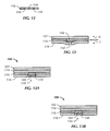
- FIG. 16 illustrates a printing process utilizing a pinch roller with a deformable section and an RFID tag with substantially uniform thickness
- FIG. 17 illustrates a printing process utilizing a pinch roller with a deformable section and an RFID tag that has a greater thickness at the location of an RFID device.
- a radio-frequency identification (RFID) tag 100 includes a face stock 102 and an RFID device 104 .
- the face stock 102 may be described as having a printable side or surface 106 and an inlay side or surface 108 .
- the RFID device 104 is mounted to or disposed on the inlay side 108 of the face stock 102 and may include any type of RFID structure, including chips, straps, power source (for active devices), and connecting structure for coupling with an antenna 110 , as known in the art.
- the face stock 102 may include an inlay substrate 114 , such as a layer of polyethylene terephthalate (PET), applied to the inlay side 108 on which the RFID device 104 (such as a microchip) and the antenna 110 may be disposed.
- a layer of adhesive 116 such as a pressure sensitive adhesive (PSA) may be coated on the inlay side 108 of the face stock 102 , and a liner 118 may be releasably adhered to the layer of adhesive 116 .
- PSA pressure sensitive adhesive
- the layer of adhesive 116 may include a blank 120 formed or defined therein that is substantially free of adhesive, as particularly shown in FIG. 4 .
- the blank 120 may be described as being spatially larger than and coincident with the RFID device 104 so that the RFID device 104 is received or located therewithin, as particularly shown in FIG. 2 .
- the blank 120 may be described as being disposed on the inlay side 108 of the face stock 102 and defining an area that is substantially free of adhesive and in which the RFID device 104 is disposed.
- the blank 120 can compensate for the thickness of the RFID device 104 , either partially or completely, as described below.
- the word blank indicated by reference numeral 120 is used to describe an area or region in the layer of adhesive 116 that is free of adhesive.
- This spatial void in the layer of adhesive 116 may be alternatively described as, for example, a window, an opening, an aperture, or a seat in the adhesive 116 .
- the tag 100 may be configured so that a thickness t is substantially uniform along a transverse axis T, as shown in FIG. 2 . Accordingly, when the tag 100 is passing through a printer 122 with a print head 124 and a pinch roller 126 , as shown in FIG. 5 , the printable side 108 of the face stock 102 remains substantially linear, or flat, along the transverse axis T of the tag as it passes between the two. In other words, any deflection of or upset in the printable side 108 of the face stock 102 caused by the RFID device 104 is minimized or substantially eliminated, thereby maintaining a printing area of the tag 100 essentially flat to enhance printing.
- the layer of adhesive 116 may have a thickness t A that is slightly greater than a thickness t D of the RFID device 104 so that the device 104 is effectively sunken within the blank 120 , leaving a small recess 128 .
- the recess 128 may provide spatial or directional accommodation in a normal direction N when the tag 100 is compressed between a print head and a pinch roller in a printer due to differing resiliency between the adhesive 116 and the RFID device 104 .
- the layer of adhesive 116 may have a thickness t A that is slightly less than a thickness t D of the RFID device 104 so that the device 104 projects out of the blank 120 slightly.
- additional spatial accommodation in the normal direction N can be accomplished by providing a liner 118 with accommodating structure, as described below.
- the liner 118 may include a relief area 130 centered about or coincident with the location of the RFID device 104 (not shown in these figures; see, e.g., FIG. 2 ), which location is indicated by L.
- the relief area 130 may include one or more weakening lines 132 .
- the weakening lines 132 may include surface scores (i.e., cuts into but not extending through the liner 118 ) or, alternatively, may include die cuts 134 that extend completely through the thickness of the liner as shown in FIG. 12 .
- the weakening lines 132 accommodate deflection of the RFID device 104 in the normal direction by allowing or enabling the liner 118 to separate and flex in the normal direction N under compression, as shown in FIG. 13 .
- the thickness of the liner 118 may range from about 2 mil to about 8 mil, and the thickness of the RFID chip 104 may range from about 5 mil to about 10 mil. For example, if the device or chip 104 is about 5 mil, then the liner 118 may be selected to be about 8 mil.
- a recess or seat 135 may be formed in the liner 118 at the location of or coincident with the RFID device 104 as shown in FIG. 13A .
- the seat 135 may be spatially larger than the RFID device 104 so that the device 104 is received within the seat as shown.
- the relief area 130 includes the seat 135 .
- the layer of adhesive 116 is relatively thin, with the thickness of the liner 118 being greater than the thickness of the device 104 . Accordingly, the device 104 is accommodated by the seat 135 of the liner 118 .
- the relief area 130 may also include the weakening lines 132 in addition to the seat 135 , if desired.
- the seat 135 may be in the form of a blank as described above in which the seat 135 is in the form of an opening through the liner 118 , as shown in FIG. 13B .
- the term relief area is used to describe an area or structure of the tag 100 that enables distortion of the tag 100 when under stress or that allows the RFID device 104 to deflect under force, thereby entering the original or normal volume of the liner 118 .
- the distortion or deflection may be either permanent or temporary.
- accommodation of deflection of an RFID tag in the normal direction N may be accomplished by a pinch roller 126 as shown in FIGS. 14 and 15 .
- the pinch roller 126 includes a body 134 that is rotatable about a transverse axis T.
- the body 134 may include a deformable section 136 disposed along a length L thereof.
- the deformable section 136 is configured to deform to a greater degree in response to a given force than the rest of the body 134 .
- the deformable section 136 is deformable, deflectable, or compressible to a greater degree than the rest of the body 134 in the normal direction N that is orthogonal to the transverse axis T.
- the deformable section 136 may also be resilient in that the deformable section 136 is able to resume its original shape or position after being compressed or deformed. In a number of embodiments in which an elastic or resilient material is used, the deformable section 136 may be described as being “softer” than the rest of the body 134 .
- the deformable section 136 may include foams such as closed-cell foams. In other embodiments, the deformable section 136 may be implemented with an electrically controllable material, such as an electro-active polymer with controllable parameters that can be softened at the deformable section 136 on command.
- an electrically controllable material such as an electro-active polymer with controllable parameters that can be softened at the deformable section 136 on command.
- the deformable section 136 does not defect in the normal direction N, and the printing side 108 is maintained substantially linear or flat along the transverse axis T for printing by the print head 124 .
- the deformable section 136 correspondingly deflects in the normal direction N to accommodate the deflection of the RFID tag 100 . Accordingly, a substantially linear or flat printing surface 108 is maintained along the transverse axis T for printing by the print head 124 .
- a normal separation S may be defined between the print head 124 and the pinch roller 126 in a normal, non-deflecting printing process.
- the pinch roller 126 can accommodate this greater thickness at the location of the RFID device 104 by increasing the separation S between the print head 124 and the pinch roller 126 by a defection separation ⁇ S, thereby maintaining the printable side 108 of the face stock 102 substantially linear or flat along the transverse axis T.
- the deformation of the deformable section 136 is temporary in that after the tag 100 has passed through the printer, the deformable section 136 returns to a normal condition under the resiliency thereof.
- the preceding embodiments of the present invention provide the foundation for numerous alternatives and modifications thereto.
- a plurality of such deformable sections may be provided.
- the entire length of the body 134 of the roller 126 may be made from a material that is substantially resilient to accommodate any local deflection of the printing stock or RFID tag 100 .
- the present invention is not limited to that precisely as shown and described in the present invention.
Abstract
Description
Claims (7)
Priority Applications (1)
| Application Number | Priority Date | Filing Date | Title |
|---|---|---|---|
| US12/430,920 US8083151B2 (en) | 2005-06-02 | 2009-04-28 | RFID tag that provides a flat print area and a pinch that enables the same |
Applications Claiming Priority (2)
| Application Number | Priority Date | Filing Date | Title |
|---|---|---|---|
| US11/144,470 US7571862B2 (en) | 2005-06-02 | 2005-06-02 | RFID tag that provides a flat print area and a pinch roller that enables the same |
| US12/430,920 US8083151B2 (en) | 2005-06-02 | 2009-04-28 | RFID tag that provides a flat print area and a pinch that enables the same |
Related Parent Applications (1)
| Application Number | Title | Priority Date | Filing Date |
|---|---|---|---|
| US11/144,470 Division US7571862B2 (en) | 2005-06-02 | 2005-06-02 | RFID tag that provides a flat print area and a pinch roller that enables the same |
Publications (2)
| Publication Number | Publication Date |
|---|---|
| US20090205515A1 US20090205515A1 (en) | 2009-08-20 |
| US8083151B2 true US8083151B2 (en) | 2011-12-27 |
Family
ID=36968229
Family Applications (2)
| Application Number | Title | Priority Date | Filing Date |
|---|---|---|---|
| US11/144,470 Expired - Fee Related US7571862B2 (en) | 2005-06-02 | 2005-06-02 | RFID tag that provides a flat print area and a pinch roller that enables the same |
| US12/430,920 Expired - Fee Related US8083151B2 (en) | 2005-06-02 | 2009-04-28 | RFID tag that provides a flat print area and a pinch that enables the same |
Family Applications Before (1)
| Application Number | Title | Priority Date | Filing Date |
|---|---|---|---|
| US11/144,470 Expired - Fee Related US7571862B2 (en) | 2005-06-02 | 2005-06-02 | RFID tag that provides a flat print area and a pinch roller that enables the same |
Country Status (2)
| Country | Link |
|---|---|
| US (2) | US7571862B2 (en) |
| WO (1) | WO2006130671A2 (en) |
Families Citing this family (9)
| Publication number | Priority date | Publication date | Assignee | Title |
|---|---|---|---|---|
| AU2004220390B8 (en) * | 2003-03-12 | 2009-12-17 | Bundesdruckerei Gmbh | Method for production of a book cover insert and a book cover insert and a book-type security document comprising a book cover insert |
| US7571862B2 (en) * | 2005-06-02 | 2009-08-11 | Avery Dennison Corporation | RFID tag that provides a flat print area and a pinch roller that enables the same |
| US7931205B2 (en) * | 2008-02-04 | 2011-04-26 | Avery Dennison Corporation | Printer with integrated RFID data collector |
| EP3207504A4 (en) * | 2014-10-14 | 2018-10-31 | Confidex Oy | Rfid transponder and rfid transponder web |
| US11443160B2 (en) | 2019-09-18 | 2022-09-13 | Sensormatic Electronics, LLC | Systems and methods for laser tuning and attaching RFID tags to products |
| US10783424B1 (en) | 2019-09-18 | 2020-09-22 | Sensormatic Electronics, LLC | Systems and methods for providing tags adapted to be incorporated with or in items |
| US11055588B2 (en) | 2019-11-27 | 2021-07-06 | Sensormatic Electronics, LLC | Flexible water-resistant sensor tag |
| US11755874B2 (en) | 2021-03-03 | 2023-09-12 | Sensormatic Electronics, LLC | Methods and systems for heat applied sensor tag |
| US11869324B2 (en) | 2021-12-23 | 2024-01-09 | Sensormatic Electronics, LLC | Securing a security tag into an article |
Citations (68)
| Publication number | Priority date | Publication date | Assignee | Title |
|---|---|---|---|---|
| US4671839A (en) * | 1985-12-23 | 1987-06-09 | Xerox Corporation | Secure identification card manufacture |
| US5026452A (en) | 1986-12-11 | 1991-06-25 | Mitsubishi Denki Kabushiki Kaisha | Method of producing IC cards |
| US5184149A (en) * | 1991-08-23 | 1993-02-02 | Nippon Aleph Corporation | Combination of magnetic card and printing apparatus therefor |
| US5250341A (en) | 1990-03-26 | 1993-10-05 | Mitsubishi Denki Kabushiki Kaisha | IC card |
| US5867102A (en) | 1997-02-27 | 1999-02-02 | Wallace Computer Services, Inc. | Electronic article surveillance label assembly and method of manufacture |
| US5982284A (en) * | 1997-09-19 | 1999-11-09 | Avery Dennison Corporation | Tag or label with laminated thin, flat, flexible device |
| US6100804A (en) | 1998-10-29 | 2000-08-08 | Intecmec Ip Corp. | Radio frequency identification system |
| US6262692B1 (en) | 1999-01-13 | 2001-07-17 | Brady Worldwide, Inc. | Laminate RFID label and method of manufacture |
| US6265977B1 (en) | 1998-09-11 | 2001-07-24 | Motorola, Inc. | Radio frequency identification tag apparatus and related method |
| US6294998B1 (en) | 2000-06-09 | 2001-09-25 | Intermec Ip Corp. | Mask construction for profile correction on an RFID smart label to improve print quality and eliminate detection |
| US6296032B1 (en) * | 1997-09-26 | 2001-10-02 | Zih Corp. | Laminator printer |
| US20020036237A1 (en) * | 2000-07-28 | 2002-03-28 | Mikoh Corporation | Materials and construction for a tamper indicating radio frequency identification label |
| US6369711B1 (en) * | 2000-06-09 | 2002-04-09 | Intermec Ip Corp | Profile corrected label with RFID transponder and method for making same |
| US6391136B1 (en) | 1998-11-18 | 2002-05-21 | X-Ident Gmbh | Method of removing units from laminate webs which have a multiplicity of units |
| US6451154B1 (en) * | 2000-02-18 | 2002-09-17 | Moore North America, Inc. | RFID manufacturing concepts |
| US20020135481A1 (en) * | 2001-03-06 | 2002-09-26 | Conwell Kevin Girard | Tamper evident smart label with RF transponder |
| US20020152860A1 (en) | 2001-04-20 | 2002-10-24 | Tamarack Products Inc. (A Delaware Corporation) | Apparatus and method for rotary pressure cutting |
| US6491227B2 (en) | 1999-05-07 | 2002-12-10 | Sony Corporation | Erroneous insertion prevention mechanism |
| US20030038174A1 (en) | 2000-12-22 | 2003-02-27 | Jones Robert L. | Identification card |
| US20030062119A1 (en) * | 2001-10-01 | 2003-04-03 | Hohberger Clive P. | Method and apparatus for associating on demand certain selected media and value-adding elements |
| US20030197064A1 (en) | 2002-04-19 | 2003-10-23 | Avery Dennison Corporation | Laser imageable RFID label/tag |
| US20040004131A1 (en) | 2000-10-24 | 2004-01-08 | Moore North America, Inc. | High temperature tag having enclosed transceiver |
| US20040094949A1 (en) | 2002-11-14 | 2004-05-20 | Savagian Michael D. | In-mold radio frequency identification device label |
| US20040104274A1 (en) * | 2002-03-18 | 2004-06-03 | Kotik Mark M. | Identification band with adhesively attached coupling elements |
| US20040169086A1 (en) | 2001-06-07 | 2004-09-02 | Eiji Ohta | Ic card |
| US6836215B1 (en) * | 2002-01-22 | 2004-12-28 | The Standard Register Company | Printable identification band with top strip for RFID chip attachment |
| US20050021172A1 (en) * | 2003-06-25 | 2005-01-27 | Intermec Ip Corp. | Method and apparatus for preparing media |
| US20050093700A1 (en) | 2003-10-30 | 2005-05-05 | Battelle Memorial Institute | Flat antenna architecture for use in radio frequency monitoring systems |
| US20050091821A1 (en) * | 2003-11-03 | 2005-05-05 | Best Scott D. | Method of manufacturing an article having a radio frequency identification (RFID) device |
| US20050101060A1 (en) | 2003-10-08 | 2005-05-12 | Shigeharu Tsunoda | Electronic device, rubber product, and methods for manufacturing the same |
| US20050128086A1 (en) * | 2003-12-08 | 2005-06-16 | 3M Innovative Properties Company | Durable radio frequency indentification label and methods of manufacturing the same |
| US20050134464A1 (en) * | 2002-06-28 | 2005-06-23 | Appleton Papers, Inc. | Thermal imaging paper laminate |
| US6911911B2 (en) | 2002-08-22 | 2005-06-28 | Schreiner Gmbh & Co., Kg | Label having an electronic circuit |
| US6995674B2 (en) | 2003-02-28 | 2006-02-07 | Saxon, Inc. | Package assembly |
| US20060028344A1 (en) | 2003-04-25 | 2006-02-09 | Forster Ian J | Extended range RFID system |
| US20060065745A1 (en) * | 2004-09-07 | 2006-03-30 | Wakahiro Kawai | Fabrication method of non-contact IC tag and apparatus of the same and non-contact IC tag |
| US20060092026A1 (en) | 2004-11-02 | 2006-05-04 | Lawrence Daniel P | Method of creating an RFID tag with substantially protected rigid electronic component |
| US20060109118A1 (en) | 2004-11-22 | 2006-05-25 | Sdgi Holdings, Inc. | Twist-tie RFID tag |
| US20060118229A1 (en) * | 2003-05-01 | 2006-06-08 | Brother Kogyo Kabushiki Kaisha | RFID label, method for producing the RFID label, device for producing the RFID label, sheet member (tag sheet) used for the RFID label, and cartridge attached to the device for producing the RFID label |
| US20060125641A1 (en) * | 2004-12-01 | 2006-06-15 | Forster Ian J | RFID tags with modifiable operating parameters |
| US20060145860A1 (en) | 2004-12-20 | 2006-07-06 | 3M Innovative Properties Company | Environmentally friendly radio frequency identification (RFID) labels and methods of using such labels |
| US20060176181A1 (en) | 2005-01-24 | 2006-08-10 | Ask S.A. | Radio frequency indentification device resistant to humid environments and its manufacturing method |
| US20060187057A1 (en) | 2005-02-09 | 2006-08-24 | San-Lien Yang | Radio frequency label module |
| US7116231B2 (en) | 2002-09-13 | 2006-10-03 | Ask S.A. | Method of producing a contactless chip card or a contact/contactless hybrid chip card with improved flatness |
| US7141451B2 (en) * | 2003-10-07 | 2006-11-28 | Hitachi, Ltd. | Wireless communication medium and method of manufacturing the same |
| US20060273170A1 (en) * | 2005-06-02 | 2006-12-07 | Forster Ian J | RFID tag that provides a flat print area and a pinch roller that enables the same |
| US20060290513A1 (en) | 2005-06-22 | 2006-12-28 | Smurfit-Stone Container Enterprises, Inc. | Methods and systems for in-line RFID transponder assembly |
| US20060292316A1 (en) | 2005-03-01 | 2006-12-28 | Kevin Conwell | Profile correction for RFID label with transponder |
| US20060290498A1 (en) * | 2005-06-23 | 2006-12-28 | Ncr Corporation | Incorporation of RFID devices into labels |
| US20070085685A1 (en) * | 2005-10-18 | 2007-04-19 | Rf Identics, Inc. | Label with electronic components and method of making same |
| US20070138281A1 (en) * | 2005-12-20 | 2007-06-21 | Satoru Moriyama | Tag-label producing device |
| US20070151660A1 (en) | 2005-12-23 | 2007-07-05 | Matt Adams | Process for manufacturing RFID label |
| US20070171129A1 (en) | 2006-01-24 | 2007-07-26 | Avery Dennison Corporation | Radio frequency (RF) antenna containing element and methods of making the same |
| US20070204493A1 (en) | 2005-01-06 | 2007-09-06 | Arkwright, Inc. | Labels for electronic devices |
| US20070210924A1 (en) | 2006-03-10 | 2007-09-13 | Wavezero, Inc. | RFID Smart Label with Reduced Layers and Method of Production |
| US20070216534A1 (en) | 2002-12-31 | 2007-09-20 | Ferguson Scott W | Rfid device and method of forming |
| US20070283556A1 (en) | 2006-06-13 | 2007-12-13 | Ncr Corporation | Method of making RFID devices |
| US7352381B2 (en) * | 2004-01-26 | 2008-04-01 | Rohm Co., Ltd. | Thermal print head |
| US20080084307A1 (en) | 2006-02-15 | 2008-04-10 | Peter Johannes M | Electronic article surveillance marker |
| US20080117056A1 (en) | 2006-11-22 | 2008-05-22 | Forster Ian J | RFID label with release liner window, and method of making |
| US20080180217A1 (en) * | 2007-01-25 | 2008-07-31 | Avery Dennison Corporation | RFID tag |
| US20080202300A1 (en) | 2005-04-25 | 2008-08-28 | Tamarack Products, Inc. | Method and Apparatus For Making Rfid Labels |
| US20080204250A1 (en) * | 2007-02-23 | 2008-08-28 | Fujitsu Limited | RFID tag |
| US20090072974A1 (en) * | 2005-10-12 | 2009-03-19 | Hiroshi Miyashita | Tape Processing Apparatus, Tag Label Producing Apparatus, Tag Assembly, and Tape Processing Method |
| US20090201158A1 (en) * | 2008-01-30 | 2009-08-13 | Tsutomu Kato | RFID tag and RFID tag producing apparatus |
| US7641606B2 (en) * | 2005-06-01 | 2010-01-05 | Canon Kabushiki Kaisha | Sheet conveyance roller and sheet processing apparatus with RFID unit embedded in the rotational member |
| US20100011978A1 (en) * | 2006-10-23 | 2010-01-21 | Fischer & Krecke Gmbh & Co. Kg | Rotary Printing Press and Method for Adjusting a Cylinder Thereof |
| US7656298B2 (en) * | 2006-01-13 | 2010-02-02 | Brother Kogyo Kabushiki Kaisha | Tag tape and tag label tape with print |
-
2005
- 2005-06-02 US US11/144,470 patent/US7571862B2/en not_active Expired - Fee Related
-
2006
- 2006-05-31 WO PCT/US2006/021091 patent/WO2006130671A2/en active Application Filing
-
2009
- 2009-04-28 US US12/430,920 patent/US8083151B2/en not_active Expired - Fee Related
Patent Citations (81)
| Publication number | Priority date | Publication date | Assignee | Title |
|---|---|---|---|---|
| US4671839A (en) * | 1985-12-23 | 1987-06-09 | Xerox Corporation | Secure identification card manufacture |
| US5026452A (en) | 1986-12-11 | 1991-06-25 | Mitsubishi Denki Kabushiki Kaisha | Method of producing IC cards |
| US5250341A (en) | 1990-03-26 | 1993-10-05 | Mitsubishi Denki Kabushiki Kaisha | IC card |
| US5184149A (en) * | 1991-08-23 | 1993-02-02 | Nippon Aleph Corporation | Combination of magnetic card and printing apparatus therefor |
| US5867102A (en) | 1997-02-27 | 1999-02-02 | Wallace Computer Services, Inc. | Electronic article surveillance label assembly and method of manufacture |
| US5867102C1 (en) | 1997-02-27 | 2002-09-10 | Wallace Comp Srvices Inc | Electronic article surveillance label assembly and method of manufacture |
| US5982284A (en) * | 1997-09-19 | 1999-11-09 | Avery Dennison Corporation | Tag or label with laminated thin, flat, flexible device |
| US6296032B1 (en) * | 1997-09-26 | 2001-10-02 | Zih Corp. | Laminator printer |
| US6265977B1 (en) | 1998-09-11 | 2001-07-24 | Motorola, Inc. | Radio frequency identification tag apparatus and related method |
| US6100804A (en) | 1998-10-29 | 2000-08-08 | Intecmec Ip Corp. | Radio frequency identification system |
| US6391136B1 (en) | 1998-11-18 | 2002-05-21 | X-Ident Gmbh | Method of removing units from laminate webs which have a multiplicity of units |
| US6262692B1 (en) | 1999-01-13 | 2001-07-17 | Brady Worldwide, Inc. | Laminate RFID label and method of manufacture |
| US6569508B2 (en) | 1999-01-13 | 2003-05-27 | Brady Worldwide, Inc. | Label having a protective cavity and method of manufacture |
| US6491227B2 (en) | 1999-05-07 | 2002-12-10 | Sony Corporation | Erroneous insertion prevention mechanism |
| US20020195194A1 (en) * | 2000-02-18 | 2002-12-26 | Moore North America, Inc.. | RFID manufacturing concepts |
| US7014729B2 (en) * | 2000-02-18 | 2006-03-21 | Moore Wallace North America, Inc. | RFID manufacturing concepts |
| US7045186B2 (en) * | 2000-02-18 | 2006-05-16 | Moore North America, Inc. | RFID manufacturing concepts |
| US6451154B1 (en) * | 2000-02-18 | 2002-09-17 | Moore North America, Inc. | RFID manufacturing concepts |
| US20020195195A1 (en) * | 2000-02-18 | 2002-12-26 | Moore North America, Inc.. | RFID manufacturing concepts |
| US6294998B1 (en) | 2000-06-09 | 2001-09-25 | Intermec Ip Corp. | Mask construction for profile correction on an RFID smart label to improve print quality and eliminate detection |
| US6369711B1 (en) * | 2000-06-09 | 2002-04-09 | Intermec Ip Corp | Profile corrected label with RFID transponder and method for making same |
| US20020036237A1 (en) * | 2000-07-28 | 2002-03-28 | Mikoh Corporation | Materials and construction for a tamper indicating radio frequency identification label |
| US20040004131A1 (en) | 2000-10-24 | 2004-01-08 | Moore North America, Inc. | High temperature tag having enclosed transceiver |
| US20030038174A1 (en) | 2000-12-22 | 2003-02-27 | Jones Robert L. | Identification card |
| US20020135481A1 (en) * | 2001-03-06 | 2002-09-26 | Conwell Kevin Girard | Tamper evident smart label with RF transponder |
| US20020152860A1 (en) | 2001-04-20 | 2002-10-24 | Tamarack Products Inc. (A Delaware Corporation) | Apparatus and method for rotary pressure cutting |
| US20040169086A1 (en) | 2001-06-07 | 2004-09-02 | Eiji Ohta | Ic card |
| US20030063139A1 (en) * | 2001-10-01 | 2003-04-03 | Hohberger Clive P. | Method and apparatus for associating on demand certain selected media and value-adding elements |
| US20030063001A1 (en) * | 2001-10-01 | 2003-04-03 | Hohberger Clive P. | Method and apparatus for associating on demand certain selected media and value-adding elements |
| US20030062119A1 (en) * | 2001-10-01 | 2003-04-03 | Hohberger Clive P. | Method and apparatus for associating on demand certain selected media and value-adding elements |
| US6836215B1 (en) * | 2002-01-22 | 2004-12-28 | The Standard Register Company | Printable identification band with top strip for RFID chip attachment |
| US20040104274A1 (en) * | 2002-03-18 | 2004-06-03 | Kotik Mark M. | Identification band with adhesively attached coupling elements |
| US20030197064A1 (en) | 2002-04-19 | 2003-10-23 | Avery Dennison Corporation | Laser imageable RFID label/tag |
| US20050134464A1 (en) * | 2002-06-28 | 2005-06-23 | Appleton Papers, Inc. | Thermal imaging paper laminate |
| US6911911B2 (en) | 2002-08-22 | 2005-06-28 | Schreiner Gmbh & Co., Kg | Label having an electronic circuit |
| US7116231B2 (en) | 2002-09-13 | 2006-10-03 | Ask S.A. | Method of producing a contactless chip card or a contact/contactless hybrid chip card with improved flatness |
| US20040094949A1 (en) | 2002-11-14 | 2004-05-20 | Savagian Michael D. | In-mold radio frequency identification device label |
| US7135979B2 (en) | 2002-11-14 | 2006-11-14 | Brady Worldwide, Inc. | In-mold radio frequency identification device label |
| US20070216534A1 (en) | 2002-12-31 | 2007-09-20 | Ferguson Scott W | Rfid device and method of forming |
| US6995674B2 (en) | 2003-02-28 | 2006-02-07 | Saxon, Inc. | Package assembly |
| US20060028344A1 (en) | 2003-04-25 | 2006-02-09 | Forster Ian J | Extended range RFID system |
| US20060118229A1 (en) * | 2003-05-01 | 2006-06-08 | Brother Kogyo Kabushiki Kaisha | RFID label, method for producing the RFID label, device for producing the RFID label, sheet member (tag sheet) used for the RFID label, and cartridge attached to the device for producing the RFID label |
| US7694883B2 (en) * | 2003-05-01 | 2010-04-13 | Brother Kogyo Kabushiki Kaisha | RFID label, method for producing the RFID label, device for producing the RFID label, sheet member (tag sheet) used for the RFID label, and cartridge attached to the device for producing the RFID label |
| US20050021172A1 (en) * | 2003-06-25 | 2005-01-27 | Intermec Ip Corp. | Method and apparatus for preparing media |
| US7141451B2 (en) * | 2003-10-07 | 2006-11-28 | Hitachi, Ltd. | Wireless communication medium and method of manufacturing the same |
| US20050101060A1 (en) | 2003-10-08 | 2005-05-12 | Shigeharu Tsunoda | Electronic device, rubber product, and methods for manufacturing the same |
| US20050093700A1 (en) | 2003-10-30 | 2005-05-05 | Battelle Memorial Institute | Flat antenna architecture for use in radio frequency monitoring systems |
| US20050091821A1 (en) * | 2003-11-03 | 2005-05-05 | Best Scott D. | Method of manufacturing an article having a radio frequency identification (RFID) device |
| US20050128086A1 (en) * | 2003-12-08 | 2005-06-16 | 3M Innovative Properties Company | Durable radio frequency indentification label and methods of manufacturing the same |
| US7352381B2 (en) * | 2004-01-26 | 2008-04-01 | Rohm Co., Ltd. | Thermal print head |
| US20060065745A1 (en) * | 2004-09-07 | 2006-03-30 | Wakahiro Kawai | Fabrication method of non-contact IC tag and apparatus of the same and non-contact IC tag |
| US20060092026A1 (en) | 2004-11-02 | 2006-05-04 | Lawrence Daniel P | Method of creating an RFID tag with substantially protected rigid electronic component |
| US20060109118A1 (en) | 2004-11-22 | 2006-05-25 | Sdgi Holdings, Inc. | Twist-tie RFID tag |
| US7170415B2 (en) * | 2004-12-01 | 2007-01-30 | Avery Dennison Corporation | RFID tags with modifiable operating parameters |
| US20060125641A1 (en) * | 2004-12-01 | 2006-06-15 | Forster Ian J | RFID tags with modifiable operating parameters |
| US20060145860A1 (en) | 2004-12-20 | 2006-07-06 | 3M Innovative Properties Company | Environmentally friendly radio frequency identification (RFID) labels and methods of using such labels |
| US20070204493A1 (en) | 2005-01-06 | 2007-09-06 | Arkwright, Inc. | Labels for electronic devices |
| US20060176181A1 (en) | 2005-01-24 | 2006-08-10 | Ask S.A. | Radio frequency indentification device resistant to humid environments and its manufacturing method |
| US20060187057A1 (en) | 2005-02-09 | 2006-08-24 | San-Lien Yang | Radio frequency label module |
| US20060292316A1 (en) | 2005-03-01 | 2006-12-28 | Kevin Conwell | Profile correction for RFID label with transponder |
| US20080202300A1 (en) | 2005-04-25 | 2008-08-28 | Tamarack Products, Inc. | Method and Apparatus For Making Rfid Labels |
| US7641606B2 (en) * | 2005-06-01 | 2010-01-05 | Canon Kabushiki Kaisha | Sheet conveyance roller and sheet processing apparatus with RFID unit embedded in the rotational member |
| US7571862B2 (en) * | 2005-06-02 | 2009-08-11 | Avery Dennison Corporation | RFID tag that provides a flat print area and a pinch roller that enables the same |
| US20060273170A1 (en) * | 2005-06-02 | 2006-12-07 | Forster Ian J | RFID tag that provides a flat print area and a pinch roller that enables the same |
| US20060290513A1 (en) | 2005-06-22 | 2006-12-28 | Smurfit-Stone Container Enterprises, Inc. | Methods and systems for in-line RFID transponder assembly |
| US20060290498A1 (en) * | 2005-06-23 | 2006-12-28 | Ncr Corporation | Incorporation of RFID devices into labels |
| US20090072974A1 (en) * | 2005-10-12 | 2009-03-19 | Hiroshi Miyashita | Tape Processing Apparatus, Tag Label Producing Apparatus, Tag Assembly, and Tape Processing Method |
| US7224278B2 (en) * | 2005-10-18 | 2007-05-29 | Avery Dennison Corporation | Label with electronic components and method of making same |
| US20070085685A1 (en) * | 2005-10-18 | 2007-04-19 | Rf Identics, Inc. | Label with electronic components and method of making same |
| US20070138281A1 (en) * | 2005-12-20 | 2007-06-21 | Satoru Moriyama | Tag-label producing device |
| US20070151660A1 (en) | 2005-12-23 | 2007-07-05 | Matt Adams | Process for manufacturing RFID label |
| US7656298B2 (en) * | 2006-01-13 | 2010-02-02 | Brother Kogyo Kabushiki Kaisha | Tag tape and tag label tape with print |
| US20070171129A1 (en) | 2006-01-24 | 2007-07-26 | Avery Dennison Corporation | Radio frequency (RF) antenna containing element and methods of making the same |
| US20080084307A1 (en) | 2006-02-15 | 2008-04-10 | Peter Johannes M | Electronic article surveillance marker |
| US20070210924A1 (en) | 2006-03-10 | 2007-09-13 | Wavezero, Inc. | RFID Smart Label with Reduced Layers and Method of Production |
| US20070283556A1 (en) | 2006-06-13 | 2007-12-13 | Ncr Corporation | Method of making RFID devices |
| US20100011978A1 (en) * | 2006-10-23 | 2010-01-21 | Fischer & Krecke Gmbh & Co. Kg | Rotary Printing Press and Method for Adjusting a Cylinder Thereof |
| US20080117056A1 (en) | 2006-11-22 | 2008-05-22 | Forster Ian J | RFID label with release liner window, and method of making |
| US20080180217A1 (en) * | 2007-01-25 | 2008-07-31 | Avery Dennison Corporation | RFID tag |
| US20080204250A1 (en) * | 2007-02-23 | 2008-08-28 | Fujitsu Limited | RFID tag |
| US20090201158A1 (en) * | 2008-01-30 | 2009-08-13 | Tsutomu Kato | RFID tag and RFID tag producing apparatus |
Non-Patent Citations (3)
| Title |
|---|
| International Preliminary Report on Patentability issued in corresponding PCT/US2006/021091 dated Dec. 21, 2007. |
| International Search Report and Written Opinion issued in corresponding PCT/US2006/021091 dated Dec. 13, 2006. |
| Invitation to Pay Additional Fees issued in corresponding PCT/US2006/021091 dated Oct. 2, 2006. |
Also Published As
| Publication number | Publication date |
|---|---|
| US20060273170A1 (en) | 2006-12-07 |
| US7571862B2 (en) | 2009-08-11 |
| WO2006130671A3 (en) | 2007-02-01 |
| WO2006130671A2 (en) | 2006-12-07 |
| US20090205515A1 (en) | 2009-08-20 |
Similar Documents
| Publication | Publication Date | Title |
|---|---|---|
| US8083151B2 (en) | RFID tag that provides a flat print area and a pinch that enables the same | |
| US6937153B2 (en) | Thermal imaging paper laminate | |
| US6114962A (en) | RF tag having strain relieved stiff substrate and hydrostatic protection for a chip mounted thereto | |
| US7364088B2 (en) | Radio frequency identification tag | |
| US20120043856A1 (en) | Piezoelectric Power Generator | |
| CN101874252B (en) | Tear protected circuit | |
| CN105701536A (en) | Contactless IC label and nameplate | |
| JP4368217B2 (en) | RFID inlet, RFID tag using the same, and seal with RFID tag | |
| US20080204196A1 (en) | Radio frequency tag and method for manufacturing radio frequency tag | |
| US20070146464A1 (en) | Printing medium, image object, and image forming method | |
| JP2002042068A (en) | Non-contact data carrier and book therewith | |
| US20060292316A1 (en) | Profile correction for RFID label with transponder | |
| JP2006277641A (en) | Ic chip interior sheet | |
| JP5169104B2 (en) | IC tag, IC tag roll | |
| JP2004355519A (en) | Ic label | |
| JP4277537B2 (en) | IC label for card type CD sticking and card type CD using the same | |
| US10843486B2 (en) | Label issuance device and antenna | |
| JP5287232B2 (en) | Inlay, inlay with cover and booklet | |
| JP2000153681A (en) | Booklet-form printed matter including non-contact type ic storing medium | |
| US8413981B2 (en) | Sheet bundle with storage tags, method of manufacturing the same, and sheet transport mechanism in image forming apparatus | |
| KR102138684B1 (en) | Method of manufacturing smart card with improved flatness and smart card thereof | |
| US20080186188A1 (en) | Label paper with rfid function and rfid tag writing apparatus | |
| JP2009116608A (en) | Medium to be printed | |
| KR102138682B1 (en) | Method of manufacturing smart card with improved the quality and smart card thereof | |
| US20060092026A1 (en) | Method of creating an RFID tag with substantially protected rigid electronic component |
Legal Events
| Date | Code | Title | Description |
|---|---|---|---|
| ZAAA | Notice of allowance and fees due |
Free format text: ORIGINAL CODE: NOA |
|
| ZAAB | Notice of allowance mailed |
Free format text: ORIGINAL CODE: MN/=. |
|
| STCF | Information on status: patent grant |
Free format text: PATENTED CASE |
|
| FPAY | Fee payment |
Year of fee payment: 4 |
|
| MAFP | Maintenance fee payment |
Free format text: PAYMENT OF MAINTENANCE FEE, 8TH YEAR, LARGE ENTITY (ORIGINAL EVENT CODE: M1552); ENTITY STATUS OF PATENT OWNER: LARGE ENTITY Year of fee payment: 8 |
|
| FEPP | Fee payment procedure |
Free format text: MAINTENANCE FEE REMINDER MAILED (ORIGINAL EVENT CODE: REM.); ENTITY STATUS OF PATENT OWNER: LARGE ENTITY |
|
| LAPS | Lapse for failure to pay maintenance fees |
Free format text: PATENT EXPIRED FOR FAILURE TO PAY MAINTENANCE FEES (ORIGINAL EVENT CODE: EXP.); ENTITY STATUS OF PATENT OWNER: LARGE ENTITY |
|
| STCH | Information on status: patent discontinuation |
Free format text: PATENT EXPIRED DUE TO NONPAYMENT OF MAINTENANCE FEES UNDER 37 CFR 1.362 |
|
| FP | Lapsed due to failure to pay maintenance fee |
Effective date: 20231227 |