US8085354B2 - Pixel structure with semiconductor of top-gate TFT extended over electrodes and liquid crystal display panel - Google Patents
Pixel structure with semiconductor of top-gate TFT extended over electrodes and liquid crystal display panel Download PDFInfo
- Publication number
- US8085354B2 US8085354B2 US12/368,966 US36896609A US8085354B2 US 8085354 B2 US8085354 B2 US 8085354B2 US 36896609 A US36896609 A US 36896609A US 8085354 B2 US8085354 B2 US 8085354B2
- Authority
- US
- United States
- Prior art keywords
- disposed
- contact hole
- pixel electrode
- dielectric layer
- layer
- Prior art date
- Legal status (The legal status is an assumption and is not a legal conclusion. Google has not performed a legal analysis and makes no representation as to the accuracy of the status listed.)
- Active, expires
Links
Images


Classifications
-
- G—PHYSICS
- G02—OPTICS
- G02F—OPTICAL DEVICES OR ARRANGEMENTS FOR THE CONTROL OF LIGHT BY MODIFICATION OF THE OPTICAL PROPERTIES OF THE MEDIA OF THE ELEMENTS INVOLVED THEREIN; NON-LINEAR OPTICS; FREQUENCY-CHANGING OF LIGHT; OPTICAL LOGIC ELEMENTS; OPTICAL ANALOGUE/DIGITAL CONVERTERS
- G02F1/00—Devices or arrangements for the control of the intensity, colour, phase, polarisation or direction of light arriving from an independent light source, e.g. switching, gating or modulating; Non-linear optics
- G02F1/01—Devices or arrangements for the control of the intensity, colour, phase, polarisation or direction of light arriving from an independent light source, e.g. switching, gating or modulating; Non-linear optics for the control of the intensity, phase, polarisation or colour
- G02F1/13—Devices or arrangements for the control of the intensity, colour, phase, polarisation or direction of light arriving from an independent light source, e.g. switching, gating or modulating; Non-linear optics for the control of the intensity, phase, polarisation or colour based on liquid crystals, e.g. single liquid crystal display cells
- G02F1/133—Constructional arrangements; Operation of liquid crystal cells; Circuit arrangements
- G02F1/1333—Constructional arrangements; Manufacturing methods
- G02F1/1335—Structural association of cells with optical devices, e.g. polarisers or reflectors
- G02F1/133553—Reflecting elements
- G02F1/133555—Transflectors
-
- G—PHYSICS
- G02—OPTICS
- G02F—OPTICAL DEVICES OR ARRANGEMENTS FOR THE CONTROL OF LIGHT BY MODIFICATION OF THE OPTICAL PROPERTIES OF THE MEDIA OF THE ELEMENTS INVOLVED THEREIN; NON-LINEAR OPTICS; FREQUENCY-CHANGING OF LIGHT; OPTICAL LOGIC ELEMENTS; OPTICAL ANALOGUE/DIGITAL CONVERTERS
- G02F1/00—Devices or arrangements for the control of the intensity, colour, phase, polarisation or direction of light arriving from an independent light source, e.g. switching, gating or modulating; Non-linear optics
- G02F1/01—Devices or arrangements for the control of the intensity, colour, phase, polarisation or direction of light arriving from an independent light source, e.g. switching, gating or modulating; Non-linear optics for the control of the intensity, phase, polarisation or colour
- G02F1/13—Devices or arrangements for the control of the intensity, colour, phase, polarisation or direction of light arriving from an independent light source, e.g. switching, gating or modulating; Non-linear optics for the control of the intensity, phase, polarisation or colour based on liquid crystals, e.g. single liquid crystal display cells
- G02F1/133—Constructional arrangements; Operation of liquid crystal cells; Circuit arrangements
- G02F1/1333—Constructional arrangements; Manufacturing methods
- G02F1/133371—Cells with varying thickness of the liquid crystal layer
-
- G—PHYSICS
- G02—OPTICS
- G02F—OPTICAL DEVICES OR ARRANGEMENTS FOR THE CONTROL OF LIGHT BY MODIFICATION OF THE OPTICAL PROPERTIES OF THE MEDIA OF THE ELEMENTS INVOLVED THEREIN; NON-LINEAR OPTICS; FREQUENCY-CHANGING OF LIGHT; OPTICAL LOGIC ELEMENTS; OPTICAL ANALOGUE/DIGITAL CONVERTERS
- G02F1/00—Devices or arrangements for the control of the intensity, colour, phase, polarisation or direction of light arriving from an independent light source, e.g. switching, gating or modulating; Non-linear optics
- G02F1/01—Devices or arrangements for the control of the intensity, colour, phase, polarisation or direction of light arriving from an independent light source, e.g. switching, gating or modulating; Non-linear optics for the control of the intensity, phase, polarisation or colour
- G02F1/13—Devices or arrangements for the control of the intensity, colour, phase, polarisation or direction of light arriving from an independent light source, e.g. switching, gating or modulating; Non-linear optics for the control of the intensity, phase, polarisation or colour based on liquid crystals, e.g. single liquid crystal display cells
- G02F1/133—Constructional arrangements; Operation of liquid crystal cells; Circuit arrangements
- G02F1/1333—Constructional arrangements; Manufacturing methods
- G02F1/1337—Surface-induced orientation of the liquid crystal molecules, e.g. by alignment layers
- G02F1/133707—Structures for producing distorted electric fields, e.g. bumps, protrusions, recesses, slits in pixel electrodes
-
- G—PHYSICS
- G02—OPTICS
- G02F—OPTICAL DEVICES OR ARRANGEMENTS FOR THE CONTROL OF LIGHT BY MODIFICATION OF THE OPTICAL PROPERTIES OF THE MEDIA OF THE ELEMENTS INVOLVED THEREIN; NON-LINEAR OPTICS; FREQUENCY-CHANGING OF LIGHT; OPTICAL LOGIC ELEMENTS; OPTICAL ANALOGUE/DIGITAL CONVERTERS
- G02F1/00—Devices or arrangements for the control of the intensity, colour, phase, polarisation or direction of light arriving from an independent light source, e.g. switching, gating or modulating; Non-linear optics
- G02F1/01—Devices or arrangements for the control of the intensity, colour, phase, polarisation or direction of light arriving from an independent light source, e.g. switching, gating or modulating; Non-linear optics for the control of the intensity, phase, polarisation or colour
- G02F1/13—Devices or arrangements for the control of the intensity, colour, phase, polarisation or direction of light arriving from an independent light source, e.g. switching, gating or modulating; Non-linear optics for the control of the intensity, phase, polarisation or colour based on liquid crystals, e.g. single liquid crystal display cells
- G02F1/133—Constructional arrangements; Operation of liquid crystal cells; Circuit arrangements
- G02F1/136—Liquid crystal cells structurally associated with a semi-conducting layer or substrate, e.g. cells forming part of an integrated circuit
- G02F1/1362—Active matrix addressed cells
- G02F1/136227—Through-hole connection of the pixel electrode to the active element through an insulation layer
-
- G—PHYSICS
- G02—OPTICS
- G02F—OPTICAL DEVICES OR ARRANGEMENTS FOR THE CONTROL OF LIGHT BY MODIFICATION OF THE OPTICAL PROPERTIES OF THE MEDIA OF THE ELEMENTS INVOLVED THEREIN; NON-LINEAR OPTICS; FREQUENCY-CHANGING OF LIGHT; OPTICAL LOGIC ELEMENTS; OPTICAL ANALOGUE/DIGITAL CONVERTERS
- G02F1/00—Devices or arrangements for the control of the intensity, colour, phase, polarisation or direction of light arriving from an independent light source, e.g. switching, gating or modulating; Non-linear optics
- G02F1/01—Devices or arrangements for the control of the intensity, colour, phase, polarisation or direction of light arriving from an independent light source, e.g. switching, gating or modulating; Non-linear optics for the control of the intensity, phase, polarisation or colour
- G02F1/13—Devices or arrangements for the control of the intensity, colour, phase, polarisation or direction of light arriving from an independent light source, e.g. switching, gating or modulating; Non-linear optics for the control of the intensity, phase, polarisation or colour based on liquid crystals, e.g. single liquid crystal display cells
- G02F1/133—Constructional arrangements; Operation of liquid crystal cells; Circuit arrangements
- G02F1/136—Liquid crystal cells structurally associated with a semi-conducting layer or substrate, e.g. cells forming part of an integrated circuit
- G02F1/1362—Active matrix addressed cells
- G02F1/1368—Active matrix addressed cells in which the switching element is a three-electrode device
- G02F1/13685—Top gates
-
- H—ELECTRICITY
- H01—ELECTRIC ELEMENTS
- H01L—SEMICONDUCTOR DEVICES NOT COVERED BY CLASS H10
- H01L27/00—Devices consisting of a plurality of semiconductor or other solid-state components formed in or on a common substrate
- H01L27/02—Devices consisting of a plurality of semiconductor or other solid-state components formed in or on a common substrate including semiconductor components specially adapted for rectifying, oscillating, amplifying or switching and having at least one potential-jump barrier or surface barrier; including integrated passive circuit elements with at least one potential-jump barrier or surface barrier
- H01L27/12—Devices consisting of a plurality of semiconductor or other solid-state components formed in or on a common substrate including semiconductor components specially adapted for rectifying, oscillating, amplifying or switching and having at least one potential-jump barrier or surface barrier; including integrated passive circuit elements with at least one potential-jump barrier or surface barrier the substrate being other than a semiconductor body, e.g. an insulating body
Definitions
- the present invention generally relates to a liquid crystal display panel (LCD panel), and more particularly, to a pixel structure in an LCD panel.
- LCD panel liquid crystal display panel
- TFT LCD thin film transistor liquid crystal display
- TN LCD twisted nematic liquid crystal display
- IPS LCD in-plane switching LCD
- FFS LCD fringe field switching LCD
- MVA LCD multi-domain vertical alignment LCD
- a plurality of alignment patterns for example, alignment protrusions or slits, are used so as to make the liquid crystal molecules in each pixel arranged in multi directions and thereby obtain different alignment domains.
- a conventional MVA LCD panel achieves the required wide-viewing angle.
- FIG. 1A is a top view diagram of a conventional LCD panel and FIG. 1B is a cross-sectional diagram of FIG. 1A along the line I 1 -I 1 ′.
- a conventional transflective multi-domain vertical alignment liquid crystal display panel (transflective MVA LCD) 100 a plurality of alignment protrusions P is disposed on the CF substrate thereof, wherein the alignment protrusions P are distributed over reflective electrodes 103 and transmissive electrodes 104 .
- a main slit SS is disposed between each transmissive electrode 104 and each reflective electrode 103 , so that the liquid crystals LC at the edges of the transmissive electrode 104 and the reflective electrode 103 tilt towards the alignment protrusion P.
- a connecting portion 105 is disposed between each reflective electrode 103 and each transmissive electrode 104 , which makes the reflective electrode 103 and the transmissive electrode 104 electrically connected to each other, wherein the material of the connecting portion 105 may be the same with that of the reflective electrode 103 or the transmissive electrode 104 .
- the above-mentioned connecting portion 105 would influence the electric field distribution in the liquid crystal layer. Under a normal operation condition, the liquid crystal molecules still can be arranged stably, but once the LCD panel is pressed and exerted by an external force, the connecting portion 105 may cause the liquid crystal molecules to be arranged in mess. That is, the liquid crystal molecules in an LCD panel are affected by the above-mentioned twisted electric field when an external force is exerted on the LCD panel and the liquid crystal molecules are unable to be quickly restored into the original arrangement, which results in apparent finger press mura and seriously affecting the quality of the LCD panel.
- the present invention is directed to a pixel structure capable of effectively mitigating the finger press mura when the invented pixel structure is used in an LCD panel.
- the present invention is also directed to an LCD panel, wherein the liquid crystal molecules can be quickly restored into the original arrangement after an external force is exerted on and presses the LCD panel.
- the present invention provides a pixel structure disposed on a substrate.
- the pixel structure includes a first pixel electrode, a second pixel electrode and a top gate thin film transistor (top gate TFT).
- the first pixel electrode and the second pixel electrode are disposed over the substrate, wherein the first pixel electrode and the second pixel electrode are separated from each other.
- the top gate TFT is disposed between the substrate and the first pixel electrode, and the top gate TFT includes a patterned semiconductor layer disposed and a gate.
- the patterned semiconductor layer is disposed on the substrate and has a plurality of conductive doping regions and at least a channel region between the conductive doping regions, wherein one of the conductive doping regions extends from below the first pixel electrode to below the second pixel electrode and is electrically connected to the first pixel electrode and the second pixel electrode.
- the gate is disposed over the channel regions.
- the present invention provides an LCD panel, which includes the above-mentioned TFT array substrate, an opposite substrate and a liquid crystal layer.
- the opposite substrate is disposed over the TFT array substrate.
- the liquid crystal layer is disposed between the TFT array substrate and the opposite substrate.
- the above-mentioned first pixel electrode and the second pixel electrode are reflective or transmissive.
- the above-mentioned patterned semiconductor layer is substantially of L-shape.
- the above-mentioned patterned semiconductor layer has three conductive doping regions and two channel regions, and each of the channel regions is respectively connected between two of the conductive doping regions.
- the above-mentioned gate is a conductive line with a branch and the conductive line is located over and covers all the channel regions.
- the above-mentioned conductive doping region electrically connected to the first pixel electrode and the second pixel electrode includes a first type doping region and a second type doping region, wherein the second type doping region is connected to the first type doping region, the first pixel electrode is electrically connected to both the first type doping region and the second type doping region, and the second pixel electrode is electrically connected to the second type doping region only.
- the above-mentioned pixel structure further includes a buffer layer disposed between the substrate and the patterned semiconductor layer.
- the above-mentioned pixel structure further includes a gate insulating layer, a first dielectric layer, a first contact conductor, a second contact conductor and a second dielectric layer.
- the gate insulating layer is disposed on the substrate to cover the patterned semiconductor layer, wherein the first dielectric layer is disposed on the gate insulating layer, a first contact hole and a second contact hole are formed within the first dielectric layer and the gate insulating layer to expose two portions of the patterned semiconductor layer, respectively.
- the first contact conductor is disposed on the first dielectric layer and electrically connected to the patterned semiconductor layer through the first contact hole.
- the second contact conductor is disposed on the first dielectric layer and electrically connected to the patterned semiconductor layer through the second contact hole.
- the second dielectric layer is disposed on the first dielectric layer, wherein the second dielectric layer has a third contact hole and a fourth contact hole to respectively expose the first contact conductor and the second contact conductor, the first pixel electrode is electrically connected to the first contact conductor through the third contact hole and the second pixel electrode is electrically connected to the second contact conductor through the fourth contact hole.
- the above-mentioned pixel structure further includes a common electrode disposed on the gate insulating layer, wherein the common electrode is overlapped with a part of the conductive doping region.
- the above-mentioned common electrode has an aperture located correspondingly to the first contact hole.
- the above-mentioned common electrode is of cross-shape.
- the above-mentioned pixel structure further includes a gate insulating layer, a first dielectric layer, a first contact conductor, a second contact conductor, a second dielectric layer and a padding layer.
- the gate insulating layer is disposed on the substrate to cover the patterned semiconductor layer, wherein the gate is disposed on the gate insulating layer, and the first dielectric layer is disposed on the gate insulating layer, a first contact hole and a second contact hole are formed within the first dielectric layer and the gate insulating layer to expose two portions of the patterned semiconductor layer, respectively.
- the first contact conductor is disposed on the first dielectric layer and electrically connected to the patterned semiconductor layer through the first contact hole.
- the second contact conductor is disposed on the first dielectric layer and electrically connected to the patterned semiconductor layer through the second contact hole.
- the second dielectric layer is disposed on the first dielectric layer.
- the padding layer is disposed on at least a part of the second dielectric layer, wherein a third contact hole is formed within the padding layer and the second dielectric to expose the first contact conductor, and the second dielectric layer has a fourth contact hole to expose the second contact conductor.
- the first pixel electrode is electrically connected to the first contact conductor through the third contact hole and the second pixel electrode is electrically connected to the second contact conductor through the fourth contact hole.
- the above-mentioned patterned semiconductor layer is comprised of poly-silicon, monocrystalline silicon, microcrystalline silicon or amorphous silicon.
- the present invention adopts the patterned semiconductor layer to deliver image data to the first pixel electrode and the second pixel electrode, so that no connecting portion is required between the first pixel electrode and the second pixel electrode, which significantly mitigate the mura after the LCD panel is pressed by an external force.
- FIG. 1A is a top view diagram of a conventional LCD panel.
- FIG. 1B is a cross-sectional diagram along the line I 1 -I 1 ′ of FIG. 1A .
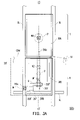
- FIG. 2A is a top view diagram of an LCD panel according to the first embodiment of the present invention.
- FIG. 2B is a cross-sectional diagram along the line I 2 -I 2 ′ of FIG. 2A .
- FIG. 2C is a localized enlargement diagram of FIG. 2B where a part of the first contact conductor and a part of the patterned semiconductor layer near the first contact hole are shown.
- FIG. 3A is a top view diagram of an LCD panel according to the second embodiment of the present invention.
- FIG. 3B is a cross-sectional diagram along the line I 3 -I 3 ′ of FIG. 3A .
- FIG. 4A is a top view diagram of an LCD panel according to the third embodiment of the present invention.
- FIG. 4B is a cross-sectional diagram along the line I 4 -I 4 ′ of FIG. 4A .
- FIG. 5A is a top view diagram of an LCD panel according to the fourth embodiment of the present invention.
- FIG. 5B is a cross-sectional diagram along the line I 5 -I 5 ′ of FIG. 5A .
- FIG. 6A is a top view diagram of an LCD panel according to the fifth embodiment of the present invention.
- FIG. 6B is a cross-sectional diagram along the line I 6 -I 6 ′ of FIG. 6A .
- FIG. 2A is a top view diagram of an LCD panel according to the first embodiment of the present invention and FIG. 2B is a cross-sectional diagram along the line I 2 -I 2 ′ of FIG. 2A .
- an LCD panel 200 of the embodiment includes a TFT array substrate 201 , an opposite substrate 202 and a liquid crystal layer 203 .
- the TFT array substrate 201 has a plurality of pixel structures 204 . Note that in FIG. 2A , only a pixel structure 204 of the TFT array substrate 201 and the opposite substrate 202 thereof are shown.
- the opposite substrate 202 is disposed over the TFT array substrate 201 , and the liquid crystal layer 203 is disposed between the TFT array substrate 201 and the opposite substrate 202 .
- the opposite substrate 202 has a plurality of alignment protrusions P so as to make the liquid crystal molecules in the liquid crystal layer 203 tilt towards the alignment protrusions P, which enables the liquid crystal molecules in each pixel arranged in multi directions and thereby obtains a plurality of different alignment domains.
- a black matrix BM is disposed over the alignment protrusions P and on the opposite substrate 202 , wherein the black matrix BM has a single layer structure or multi-layers structure and is made of, for example, metal, organic material, color photoresist material or a combination of the above-mentioned materials.
- the black matrix BM is formed by stacking a plurality of color photorsist layers.
- the TFT array substrate 201 includes a pixel structure 204 , and the pixel structure 204 includes a first pixel electrode 205 , a second pixel electrode 206 and a top gate TFT 207 .
- the pixel structure 204 has a reflective region R and a transmissive region T.
- the first pixel electrode 205 is a reflective pixel electrode located in the reflective region R and the second pixel electrode 206 is a transmissive pixel electrode located in the transmissive region T.
- the alignment protrusions P of the opposite substrate 202 are respectively located over the first pixel electrode 205 and the second pixel electrode 206 .
- the pixel electrode 206 within the transmissive region T serves as a transparent electrode, so that the light emitted from a backlight source can pass through the pixel electrode 206 .
- the pixel electrode 205 located in the reflective region R is a metal reflective electrode or other reflective electrodes made of materials with good reflectivity so as to achieve the displaying effect by reflecting the light emitted from a front-light source and/or an environmental light source.
- the first pixel electrode 205 is an aluminium electrode, for example, with bumps formed on the surface thereof, and the second pixel electrode 206 serving as a transmissive pixel electrode is made of indium-tin oxide (ITO) or indium-zinc oxide (IZO), for example.
- ITO indium-tin oxide
- IZO indium-zinc oxide
- a continuous main slit SS is located between the first pixel electrode 205 and the second pixel electrode 206 to physically separate the two pixel electrodes 205 and 206 from each other.
- the present invention is not limited to the material and the number of the above-mentioned pixel electrode of the embodiment.
- the pixel structure 204 can further include a gate insulating layer 209 , a buffer layer 210 , a first dielectric layer 211 , a first contact conductor M 1 , a second contact conductor M 2 , a second dielectric layer 212 and a common electrode COM.
- the top gate TFT 207 is disposed between the TFT array substrate 201 and the first pixel electrode 205 and includes a patterned semiconductor layer 208 and a gate G.
- the patterned semiconductor layer 208 herein extends from below the first pixel electrode 205 to below the second pixel electrode 206 and is electrically connected to the first pixel electrode 205 and the second pixel electrode 206 .
- the patterned semiconductor layer 208 is comprised of poly-silicon, monocrystalline silicon, microcrystalline silicon or amorphous silicon, for example.
- the buffer layer 210 is optionally disposed between the substrate 201 and the patterned semiconductor layer 208 , as shown in FIG. 2B .
- the gate insulating layer 209 is disposed on the substrate 201 to cover the patterned semiconductor layer 208 , wherein the gate G is disposed on the gate insulating layer 209 .
- the first dielectric layer 211 is disposed on the gate insulating layer 209 , wherein a first contact hole W 1 and a second contact hole W 2 are formed within the first dielectric layer 211 and the gate insulating layer 209 to expose two portions of the patterned semiconductor layer 208 , respectively.
- the first contact conductor M 1 is disposed on the first dielectric layer 211 and is electrically connected to the patterned semiconductor layer 208 through the first contact hole W 1 .
- the second contact conductor M 2 is disposed on the first dielectric layer 211 and is electrically connected to the patterned semiconductor layer 208 through the second contact hole W 2 .
- the second dielectric layer 212 is disposed on the first dielectric layer 211 and has a third contact hole W 3 and a fourth contact hole W 4 to respectively expose the first contact conductor M 1 and the second contact conductor M 2 .
- the first pixel electrode 205 is electrically connected to the first contact conductor M 1 through the third contact hole W 3
- the second pixel electrode 206 is electrically connected to the second contact conductor M 2 through the fourth contact hole W 4 .
- the positions of the second contact hole W 2 , the fourth contact hole W 4 and the second contact conductor M 2 are corresponding to the positions of the alignment protrusions P of the opposite substrate 202 .
- the black matrix BM over the alignment protrusions P can effectively shield the leakage light around the fourth contact hole W 4 and the second contact conductor M 2 can effectively shield the leakage light around the alignment protrusions P.
- the second contact hole W 2 can be aligned with or staggered from the fourth contact hole W 4 according to different panel processes.
- the first contact hole W 1 can be aligned with or staggered from the third contact hole W 3 .
- the common electrode COM is disposed on the gate insulating layer 209 and overlapped with the patterned semiconductor layer 208 . More specifically, the common electrode COM is overlapped with a part of the patterned semiconductor layer 208 , and the gate insulating layer 209 is located between the common electrode COM and the part of the patterned semiconductor layer 208 , such that the common electrode COM together with the part of the patterned semiconductor layer 208 forms a storage capacitor Cst.
- the top gate TFT 207 is turned on and an image signal is transmitted from a data line DL to the contact hole W in the first dielectric layer 211 . Then, the image signal transmitted by the data line DL is transmitted to the patterned semiconductor layer 208 through the contact hole W. Next, the image signal is transmitted to the second contact conductor M 2 formed in the second contact hole W 2 and the first contact conductor M 1 formed in the first contact hole W 1 though the patterned semiconductor layer 208 . As shown in FIGS.
- the patterned semiconductor layer 208 can transmit the image signals from the data line DL to the first pixel electrode 205 and the second pixel electrode 206 .
- the patterned semiconductor layer 208 directly transmits the image signal from the data line DL to the electrodes 206 and 205 respectively located in the transmissive region T and the reflective region R through the contact holes W 1 -W 4 and the contact conductors M 1 and M 2 , which is different from the prior art where a connecting potion 105 (as shown in FIG. 1B ) is used to transmit the image signals.
- the patterned semiconductor layer 208 is substantially of L-shape and has a plurality of conductive doping regions 208 a , 208 b and 208 c and two channel regions 208 ′ and 208 ′′ between the conductive doping regions, wherein the conductive doping region 208 c extends from below the first pixel electrode 205 to below the second pixel electrode 206 and is electrically connected to the first pixel electrode 205 and the second pixel electrode 206 .
- the gate G is, for example, a conductive line with a branch, which is located over the above-mentioned channel regions 208 ′ and 208 ′′ to cover channel regions 208 ′ and 208 ′′ so as to form a plurality of top gates TFT 207 .
- FIG. 2C is a localized enlargement diagram of FIG. 2B where a part of the first contact conductor and a part of the patterned semiconductor layer near the first contact hole are shown.
- the first contact conductor M 1 is disposed on the first dielectric layer 211 and is electrically connected to the patterned semiconductor layer 208 through the first contact hole W 1 .
- the conductive doping region 208 c electrically connected to both the first pixel electrode 205 and the second pixel electrode 206 includes a first type doping region D 1 and a second type doping region D 2 .
- the second type doping region D 2 is connected to the first type doping region D 1 , wherein the first pixel electrode 205 is electrically connected to both the first type doping region D 1 and the second type doping region D 2 , and the second pixel electrode 206 is electrically connected to second type doping region D 2 only.
- the conductive doping region 208 c of the storage capacitor Cst has, for example, both N-type doped sub-region and P-type doped sub-region.
- the two different doping sub-regions share a border right below the first contact hole W 1 , for example, first type doping region D 1 and the second type doping region D 2 . Since the junction (i.e., the above-mentioned border) between the first type doping region D 1 and the second type doping region D 2 is a P-N junction J, so that a depletion region L is formed at the junction which is unfavourable to conduct current.
- the embodiment utilizes the first contact conductor M 1 electrically connected to the conductive doping region 208 c through the first contact hole W 1 to provide another current conductive path. In this way, when the patterned semiconductor layer 208 transmits the image signals to the first pixel electrode 205 and the second pixel electrode 206 , the possible negative impact by the depletion region L of the p-n junction J can be avoided.
- the embodiment uses the patterned semiconductor layer 208 to transmit image signals to the first pixel electrode 205 and the second pixel electrode 206 , which effectively avoids the serious twist of the electric field occurred near the connecting portion 105 and mitigates the finger press mura.
- FIG. 3A is a top view diagram of an LCD panel according to the second embodiment of the present invention and FIG. 3B is a cross-sectional diagram along the line I 3 -I 3 ′ of FIG. 3A .
- an LCD panel 200 b of the embodiment is similar to the LCD panel 200 of the first embodiment except that an alignment pattern SCF is disposed over the first pixel electrode 205 in the LCD panel 200 b .
- the alignment pattern SCF is disposed on the opposite substrate 202 and an alignment protrusion P is disposed below the alignment pattern SCF.
- the liquid crystal molecules in each pixel are arranged in multi directions by using an alignment pattern SCF together with a plurality of alignment protrusions P and thereby a plurality of different alignment domains is obtained so as to achieve the required wide-viewing angle.
- the cell-gaps of the liquid crystal layer 203 within the reflective region R can be changed so that the transflective pixel structure 204 of the embodiment is modified into a dual cell-gaps structure; that is, the transmissive region T and the reflective region R respectively have a liquid crystal layer 203 having different thicknesses.
- the cell gap of the liquid crystal layer 203 within the transmissive region T is G 1 and the cell gap of the liquid crystal layer 203 within the reflective region R in the first embodiment is also G 1 before disposing the alignment pattern SCF.
- the cell gap of the liquid crystal layer 203 within the reflective region R in the second embodiment is changed to G 2 , wherein G 2 is a half of G 1 .
- the dual cell-gaps structure provided by the embodiment enables the transmissive region T and the reflective region R to have substantially the same phase retardation, which further enhances the display quality of the transflective LCD panel 200 b.
- FIG. 4A is a top view diagram of an LCD panel according to the third embodiment of the present invention and FIG. 4B is a cross-sectional diagram along the line I 4 -I 4 ′ of FIG. 4A .
- an LCD panel 200 c of the embodiment is similar to the LCD panel 200 b of the second embodiment except that a padding layer 213 located in the reflective region R of the LCD panel 200 c is disposed on a part of the second dielectric layer 212 .
- the pixel structure 204 of the embodiment further includes a gate insulating layer 209 , a first dielectric layer 211 , a first contact conductor M 1 , a second contact conductor M 2 , a second dielectric layer 212 and a padding layer 213 .
- the gate insulating layer 209 covers the patterned semiconductor layer 208 , wherein the gate G is disposed on the gate insulating layer 209 .
- the first dielectric layer 211 is disposed on the gate insulating layer 209 , wherein a first contact hole W 1 and a second contact hole W 2 are formed within the first dielectric layer 211 and the gate insulating layer 209 to expose two portions of the patterned semiconductor layer 208 , respectively.
- the first contact conductor M 1 is disposed on the first dielectric layer 211 and is electrically connected to the patterned semiconductor layer 208 through the first contact hole W 1 .
- the second contact conductor M 2 is disposed on the first dielectric layer 211 and is electrically connected to the patterned semiconductor layer 208 through the second contact hole W 2 .
- the second dielectric layer 212 is disposed on the first dielectric layer 211 .
- the padding layer 213 is disposed on a part of the second dielectric layer 212 , wherein a third contact hole W 3 is formed within the padding layer 213 and the second dielectric layer 212 to expose the first contact conductor M 1 .
- the second dielectric layer 212 has a fourth contact hole W 4 to expose the second contact conductor M 2 .
- the first pixel electrode 205 is electrically connected to the first contact conductor M 1 through the third contact hole W 3
- the second pixel electrode 206 is electrically connected to the second contact conductor M 2 through the fourth contact hole W 4 .
- the padding layer 213 functions similarly to the alignment pattern SCF of the second embodiment.
- the cell gap G 2 ′ of the liquid crystal layer within the reflective region R is adjusted by the padding layer 213 , wherein G 2 ′ is a half of cell gap G 1 of the liquid crystal layer within the transmissive region T, so that the display quality of the transflective LCD panel 200 c is further promoted.
- FIG. 5A is a top view diagram of an LCD panel according to the fourth embodiment of the present invention and FIG. 5B is a cross-sectional diagram along the line I 5 -I 5 ′ of FIG. 5A .
- an LCD panel 200 d of the embodiment is similar to the LCD panel 200 of the first embodiment except that both the first pixel electrode 205 and the second pixel electrode 206 of the LCD panel 200 d are transmissive pixel electrodes.
- the pixel structure 204 of the LCD panel 200 d has two transmissive regions T 1 and T 2 .
- both the first pixel electrode 205 and the second pixel electrode 206 of the LCD panel can be reflective pixel electrodes as well.
- FIG. 5B another difference of the LCD panel 200 d from the LCD panel 200 of the first embodiment rests in that the common electrode COM of the embodiment is disposed on the gate insulating layer 209 and has an aperture 214 at the position of the first contact hole W 1 , wherein the common electrode COM is overlapped with a part of the conductive doping region 208 to form a storage capacitor Cst.
- FIG. 6A is a top view diagram of an LCD panel according to the fifth embodiment of the present invention and FIG. 6B is a cross-sectional diagram along the line I 6 -I 6 ′ of FIG. 6A .
- an LCD panel 200 e of the embodiment is similar to the LCD panel 200 d of the fourth embodiment except that the common electrode COM of the pixel structure 204 in the embodiment is of cross-shape.
- the common electrode COM is distributed not only below the main slit SS between the first transmissive region T 1 and the second transmissive region T 2 , but also on the linking line between the third contact hole W 3 and the fourth contact hole W 4 , wherein the common electrode COM in cross-shape is able to increase the capacitance of the storage capacitor Cst.
- the LCD panel of the present invention has at least following advantages:
- the present invention adopts the patterned semiconductor layer to transmit image signal to the first pixel electrode and the second pixel electrode without using a connecting portion; therefore, the liquid crystal molecules are not affected by twist electric field caused by the conventional connecting portion, which is favourable to mitigate the finger press mura after the LCD panel is pressed by an external force.
- the pixel structure can be changed into a dual cell-gaps structure by design depending on the application requirement, which promotes the display quality of the transflective LCD panel.
- a common electrode in cross-shape is used to increase the capacitance of the storage capacitor Cst, so as to reduce the voltage variation caused by a capacitor coupling effect, which further enhances the display quality of the panel.
Abstract
Description
Claims (20)
Applications Claiming Priority (3)
| Application Number | Priority Date | Filing Date | Title |
|---|---|---|---|
| TW097131633A TWI374325B (en) | 2008-08-19 | 2008-08-19 | Liquid crystal display panel and pixel structure thereof |
| TW97131633 | 2008-08-19 | ||
| TW97131633A | 2008-08-19 |
Publications (2)
| Publication Number | Publication Date |
|---|---|
| US20100044716A1 US20100044716A1 (en) | 2010-02-25 |
| US8085354B2 true US8085354B2 (en) | 2011-12-27 |
Family
ID=41695523
Family Applications (1)
| Application Number | Title | Priority Date | Filing Date |
|---|---|---|---|
| US12/368,966 Active 2030-04-04 US8085354B2 (en) | 2008-08-19 | 2009-02-10 | Pixel structure with semiconductor of top-gate TFT extended over electrodes and liquid crystal display panel |
Country Status (2)
| Country | Link |
|---|---|
| US (1) | US8085354B2 (en) |
| TW (1) | TWI374325B (en) |
Families Citing this family (4)
| Publication number | Priority date | Publication date | Assignee | Title |
|---|---|---|---|---|
| TWI432837B (en) * | 2011-01-31 | 2014-04-01 | Chunghwa Picture Tubes Ltd | Display panel |
| CN104020616B (en) * | 2014-06-04 | 2016-08-24 | 京东方科技集团股份有限公司 | Transmitting/reflecting LCD and driving method thereof |
| US9798202B2 (en) * | 2016-03-11 | 2017-10-24 | Shenzhen China Star Optoelectronics Technology Co., Ltd. | FFS mode array substrate with TFT channel layer and common electrode layer patterned from a single semiconductor layer and manufacturing method thereof |
| JP7331614B2 (en) | 2019-10-16 | 2023-08-23 | 凸版印刷株式会社 | liquid crystal display |
Citations (7)
| Publication number | Priority date | Publication date | Assignee | Title |
|---|---|---|---|---|
| US20050185120A1 (en) | 2004-02-19 | 2005-08-25 | Sharp Kabushiki Kaisha | Liquid crystal display device |
| US20060091387A1 (en) | 1998-11-25 | 2006-05-04 | Semiconductor Energy Laboratory Co., Ltd. | Semiconductor device |
| US20060268186A1 (en) | 2004-12-28 | 2006-11-30 | Tsuyoshi Kamada | Substrate for liquid crystal display device, liquid crystal display device having same, and driving method of liquid crystal display device |
| US7250996B2 (en) | 2003-12-09 | 2007-07-31 | Fujitsu Limited | Liquid crystal display and method of manufacturing the same |
| US20080121893A1 (en) * | 2006-11-23 | 2008-05-29 | Chul-Ho Kim | Display panel |
| US20080239227A1 (en) * | 2007-03-27 | 2008-10-02 | Au Optronics Corporation | Pixel Structure, Display Panel, Electro-Optical Device, and Method for Manufacturing the Same |
| US20090079892A1 (en) * | 2007-09-20 | 2009-03-26 | Chi Mei Optoelectronic Inc. | Pixel Array Substrate and Liquid Crystal Display |
-
2008
- 2008-08-19 TW TW097131633A patent/TWI374325B/en active
-
2009
- 2009-02-10 US US12/368,966 patent/US8085354B2/en active Active
Patent Citations (7)
| Publication number | Priority date | Publication date | Assignee | Title |
|---|---|---|---|---|
| US20060091387A1 (en) | 1998-11-25 | 2006-05-04 | Semiconductor Energy Laboratory Co., Ltd. | Semiconductor device |
| US7250996B2 (en) | 2003-12-09 | 2007-07-31 | Fujitsu Limited | Liquid crystal display and method of manufacturing the same |
| US20050185120A1 (en) | 2004-02-19 | 2005-08-25 | Sharp Kabushiki Kaisha | Liquid crystal display device |
| US20060268186A1 (en) | 2004-12-28 | 2006-11-30 | Tsuyoshi Kamada | Substrate for liquid crystal display device, liquid crystal display device having same, and driving method of liquid crystal display device |
| US20080121893A1 (en) * | 2006-11-23 | 2008-05-29 | Chul-Ho Kim | Display panel |
| US20080239227A1 (en) * | 2007-03-27 | 2008-10-02 | Au Optronics Corporation | Pixel Structure, Display Panel, Electro-Optical Device, and Method for Manufacturing the Same |
| US20090079892A1 (en) * | 2007-09-20 | 2009-03-26 | Chi Mei Optoelectronic Inc. | Pixel Array Substrate and Liquid Crystal Display |
Also Published As
| Publication number | Publication date |
|---|---|
| TWI374325B (en) | 2012-10-11 |
| TW201009466A (en) | 2010-03-01 |
| US20100044716A1 (en) | 2010-02-25 |
Similar Documents
| Publication | Publication Date | Title |
|---|---|---|
| US7978296B2 (en) | Liquid crystal display and thin film transistor substrate therefor | |
| KR101112537B1 (en) | Liquid crystal display having multi domain and panel for the same | |
| JPWO2005006068A1 (en) | Display device | |
| US20100141885A1 (en) | Liquid crystal display of fringe field switching type | |
| US8610856B2 (en) | Liquid crystal display device | |
| US20130321736A1 (en) | Liquid crystal display | |
| US8085354B2 (en) | Pixel structure with semiconductor of top-gate TFT extended over electrodes and liquid crystal display panel | |
| US7388638B2 (en) | TFT substrate and liquid crystal display device having the same comprising a plurality of patterns disposed at different heights | |
| US8773604B2 (en) | Horizontal electric field type liquid crystal display wherein a pixel common electrode is contacted with a common electrode pattern in a non-display pixel area where a width of a gate line narrows | |
| JPWO2009101732A1 (en) | Liquid crystal display device | |
| KR20050098631A (en) | Liquid crystal display and panel for the same | |
| US10025137B2 (en) | Liquid crystal display device having transmitting region and reflecting region | |
| US7855771B2 (en) | Liquid crystal display panel and active matrix substrate thereof | |
| US10401684B2 (en) | Liquid crystal display device | |
| KR20080097543A (en) | Liquid crystal display | |
| KR101189280B1 (en) | Display device | |
| KR100984346B1 (en) | Liquid crystal display having multi domain and panel for the same | |
| JP4711439B2 (en) | Display device | |
| KR20060038078A (en) | Thin film transistor array panel and multi domain liquid crystal display including the same | |
| KR20050076402A (en) | Liquid crystal display and thin film transistor array panel therefor | |
| KR20060020893A (en) | Multi-domain thin film transistor array panel | |
| KR20050078761A (en) | Liquid crystal display and panel for the same | |
| KR20050121881A (en) | Liquid crystal display and panel for the same | |
| KR20080054573A (en) | Display device | |
| KR20060012207A (en) | Panel and multi-domain liquid crystal display including the same |
Legal Events
| Date | Code | Title | Description |
|---|---|---|---|
| AS | Assignment |
Owner name: AU OPTRONICS CORPORATION,TAIWAN Free format text: ASSIGNMENT OF ASSIGNORS INTEREST;ASSIGNORS:LO, CHENG;FAN JIANG, SHIH-CHYUAN;CHENG, CHING-SHENG;AND OTHERS;SIGNING DATES FROM 20090105 TO 20090109;REEL/FRAME:022278/0912 Owner name: AU OPTRONICS CORPORATION, TAIWAN Free format text: ASSIGNMENT OF ASSIGNORS INTEREST;ASSIGNORS:LO, CHENG;FAN JIANG, SHIH-CHYUAN;CHENG, CHING-SHENG;AND OTHERS;SIGNING DATES FROM 20090105 TO 20090109;REEL/FRAME:022278/0912 |
|
| STCF | Information on status: patent grant |
Free format text: PATENTED CASE |
|
| FPAY | Fee payment |
Year of fee payment: 4 |
|
| MAFP | Maintenance fee payment |
Free format text: PAYMENT OF MAINTENANCE FEE, 8TH YEAR, LARGE ENTITY (ORIGINAL EVENT CODE: M1552); ENTITY STATUS OF PATENT OWNER: LARGE ENTITY Year of fee payment: 8 |
|
| MAFP | Maintenance fee payment |
Free format text: PAYMENT OF MAINTENANCE FEE, 12TH YEAR, LARGE ENTITY (ORIGINAL EVENT CODE: M1553); ENTITY STATUS OF PATENT OWNER: LARGE ENTITY Year of fee payment: 12 |