US8088656B2 - Fabricating ESD devices using MOSFET and LDMOS - Google Patents
Fabricating ESD devices using MOSFET and LDMOS Download PDFInfo
- Publication number
- US8088656B2 US8088656B2 US12/541,484 US54148409A US8088656B2 US 8088656 B2 US8088656 B2 US 8088656B2 US 54148409 A US54148409 A US 54148409A US 8088656 B2 US8088656 B2 US 8088656B2
- Authority
- US
- United States
- Prior art keywords
- ion
- type
- ion implantation
- well
- implantations
- Prior art date
- Legal status (The legal status is an assumption and is not a legal conclusion. Google has not performed a legal analysis and makes no representation as to the accuracy of the status listed.)
- Expired - Fee Related
Links
- 238000005468 ion implantation Methods 0.000 claims abstract description 210
- 239000000758 substrate Substances 0.000 claims abstract description 41
- 238000000034 method Methods 0.000 claims abstract description 22
- 239000004065 semiconductor Substances 0.000 claims abstract description 15
- 238000002955 isolation Methods 0.000 claims description 22
- 230000005669 field effect Effects 0.000 claims description 6
- 239000007943 implant Substances 0.000 claims description 4
- 229910052710 silicon Inorganic materials 0.000 claims description 4
- 239000010703 silicon Substances 0.000 claims description 4
- XUIMIQQOPSSXEZ-UHFFFAOYSA-N Silicon Chemical compound [Si] XUIMIQQOPSSXEZ-UHFFFAOYSA-N 0.000 claims description 3
- 230000003247 decreasing effect Effects 0.000 claims description 3
- 229910052751 metal Inorganic materials 0.000 description 40
- 239000002184 metal Substances 0.000 description 40
- 229910021332 silicide Inorganic materials 0.000 description 40
- FVBUAEGBCNSCDD-UHFFFAOYSA-N silicide(4-) Chemical compound [Si-4] FVBUAEGBCNSCDD-UHFFFAOYSA-N 0.000 description 40
- 238000004519 manufacturing process Methods 0.000 description 16
- 239000002019 doping agent Substances 0.000 description 10
- 229910001423 beryllium ion Inorganic materials 0.000 description 6
- 229920002120 photoresistant polymer Polymers 0.000 description 6
- 229910052796 boron Inorganic materials 0.000 description 5
- 150000002500 ions Chemical class 0.000 description 4
- ZOXJGFHDIHLPTG-UHFFFAOYSA-N Boron Chemical compound [B] ZOXJGFHDIHLPTG-UHFFFAOYSA-N 0.000 description 3
- 230000015572 biosynthetic process Effects 0.000 description 2
- 238000010586 diagram Methods 0.000 description 2
- 238000009826 distribution Methods 0.000 description 2
- 238000012986 modification Methods 0.000 description 2
- 230000004048 modification Effects 0.000 description 2
- 229910021420 polycrystalline silicon Inorganic materials 0.000 description 2
- 229920005591 polysilicon Polymers 0.000 description 2
- 125000006850 spacer group Chemical group 0.000 description 2
- OAICVXFJPJFONN-UHFFFAOYSA-N Phosphorus Chemical compound [P] OAICVXFJPJFONN-UHFFFAOYSA-N 0.000 description 1
- 238000000137 annealing Methods 0.000 description 1
- 229910052785 arsenic Inorganic materials 0.000 description 1
- RQNWIZPPADIBDY-UHFFFAOYSA-N arsenic atom Chemical compound [As] RQNWIZPPADIBDY-UHFFFAOYSA-N 0.000 description 1
- 230000015556 catabolic process Effects 0.000 description 1
- 230000000295 complement effect Effects 0.000 description 1
- 230000006378 damage Effects 0.000 description 1
- 230000007812 deficiency Effects 0.000 description 1
- 238000009792 diffusion process Methods 0.000 description 1
- 230000003993 interaction Effects 0.000 description 1
- 229910021421 monocrystalline silicon Inorganic materials 0.000 description 1
- 229910052698 phosphorus Inorganic materials 0.000 description 1
- 239000011574 phosphorus Substances 0.000 description 1
- 230000008707 rearrangement Effects 0.000 description 1
- 229920006395 saturated elastomer Polymers 0.000 description 1
- 238000006467 substitution reaction Methods 0.000 description 1
Images


Classifications
-
- H—ELECTRICITY
- H01—ELECTRIC ELEMENTS
- H01L—SEMICONDUCTOR DEVICES NOT COVERED BY CLASS H10
- H01L21/00—Processes or apparatus adapted for the manufacture or treatment of semiconductor or solid state devices or of parts thereof
- H01L21/70—Manufacture or treatment of devices consisting of a plurality of solid state components formed in or on a common substrate or of parts thereof; Manufacture of integrated circuit devices or of parts thereof
- H01L21/77—Manufacture or treatment of devices consisting of a plurality of solid state components or integrated circuits formed in, or on, a common substrate
- H01L21/78—Manufacture or treatment of devices consisting of a plurality of solid state components or integrated circuits formed in, or on, a common substrate with subsequent division of the substrate into plural individual devices
- H01L21/82—Manufacture or treatment of devices consisting of a plurality of solid state components or integrated circuits formed in, or on, a common substrate with subsequent division of the substrate into plural individual devices to produce devices, e.g. integrated circuits, each consisting of a plurality of components
- H01L21/822—Manufacture or treatment of devices consisting of a plurality of solid state components or integrated circuits formed in, or on, a common substrate with subsequent division of the substrate into plural individual devices to produce devices, e.g. integrated circuits, each consisting of a plurality of components the substrate being a semiconductor, using silicon technology
- H01L21/8232—Field-effect technology
- H01L21/8234—MIS technology, i.e. integration processes of field effect transistors of the conductor-insulator-semiconductor type
- H01L21/8238—Complementary field-effect transistors, e.g. CMOS
- H01L21/823892—Complementary field-effect transistors, e.g. CMOS with a particular manufacturing method of the wells or tubs, e.g. twin tubs, high energy well implants, buried implanted layers for lateral isolation [BILLI]
-
- H—ELECTRICITY
- H01—ELECTRIC ELEMENTS
- H01L—SEMICONDUCTOR DEVICES NOT COVERED BY CLASS H10
- H01L21/00—Processes or apparatus adapted for the manufacture or treatment of semiconductor or solid state devices or of parts thereof
- H01L21/70—Manufacture or treatment of devices consisting of a plurality of solid state components formed in or on a common substrate or of parts thereof; Manufacture of integrated circuit devices or of parts thereof
- H01L21/77—Manufacture or treatment of devices consisting of a plurality of solid state components or integrated circuits formed in, or on, a common substrate
- H01L21/78—Manufacture or treatment of devices consisting of a plurality of solid state components or integrated circuits formed in, or on, a common substrate with subsequent division of the substrate into plural individual devices
- H01L21/82—Manufacture or treatment of devices consisting of a plurality of solid state components or integrated circuits formed in, or on, a common substrate with subsequent division of the substrate into plural individual devices to produce devices, e.g. integrated circuits, each consisting of a plurality of components
- H01L21/822—Manufacture or treatment of devices consisting of a plurality of solid state components or integrated circuits formed in, or on, a common substrate with subsequent division of the substrate into plural individual devices to produce devices, e.g. integrated circuits, each consisting of a plurality of components the substrate being a semiconductor, using silicon technology
- H01L21/8232—Field-effect technology
- H01L21/8234—MIS technology, i.e. integration processes of field effect transistors of the conductor-insulator-semiconductor type
- H01L21/8238—Complementary field-effect transistors, e.g. CMOS
- H01L21/823814—Complementary field-effect transistors, e.g. CMOS with a particular manufacturing method of the source or drain structures, e.g. specific source or drain implants or silicided source or drain structures or raised source or drain structures
-
- H—ELECTRICITY
- H01—ELECTRIC ELEMENTS
- H01L—SEMICONDUCTOR DEVICES NOT COVERED BY CLASS H10
- H01L29/00—Semiconductor devices adapted for rectifying, amplifying, oscillating or switching, or capacitors or resistors with at least one potential-jump barrier or surface barrier, e.g. PN junction depletion layer or carrier concentration layer; Details of semiconductor bodies or of electrodes thereof ; Multistep manufacturing processes therefor
- H01L29/66—Types of semiconductor device ; Multistep manufacturing processes therefor
- H01L29/66007—Multistep manufacturing processes
- H01L29/66075—Multistep manufacturing processes of devices having semiconductor bodies comprising group 14 or group 13/15 materials
- H01L29/66227—Multistep manufacturing processes of devices having semiconductor bodies comprising group 14 or group 13/15 materials the devices being controllable only by the electric current supplied or the electric potential applied, to an electrode which does not carry the current to be rectified, amplified or switched, e.g. three-terminal devices
- H01L29/66409—Unipolar field-effect transistors
- H01L29/66477—Unipolar field-effect transistors with an insulated gate, i.e. MISFET
- H01L29/66568—Lateral single gate silicon transistors
- H01L29/66659—Lateral single gate silicon transistors with asymmetry in the channel direction, e.g. lateral high-voltage MISFETs with drain offset region, extended drain MISFETs
-
- H—ELECTRICITY
- H01—ELECTRIC ELEMENTS
- H01L—SEMICONDUCTOR DEVICES NOT COVERED BY CLASS H10
- H01L29/00—Semiconductor devices adapted for rectifying, amplifying, oscillating or switching, or capacitors or resistors with at least one potential-jump barrier or surface barrier, e.g. PN junction depletion layer or carrier concentration layer; Details of semiconductor bodies or of electrodes thereof ; Multistep manufacturing processes therefor
- H01L29/66—Types of semiconductor device ; Multistep manufacturing processes therefor
- H01L29/68—Types of semiconductor device ; Multistep manufacturing processes therefor controllable by only the electric current supplied, or only the electric potential applied, to an electrode which does not carry the current to be rectified, amplified or switched
- H01L29/76—Unipolar devices, e.g. field effect transistors
- H01L29/772—Field effect transistors
- H01L29/78—Field effect transistors with field effect produced by an insulated gate
- H01L29/7833—Field effect transistors with field effect produced by an insulated gate with lightly doped drain or source extension, e.g. LDD MOSFET's; DDD MOSFET's
- H01L29/7835—Field effect transistors with field effect produced by an insulated gate with lightly doped drain or source extension, e.g. LDD MOSFET's; DDD MOSFET's with asymmetrical source and drain regions, e.g. lateral high-voltage MISFETs with drain offset region, extended drain MISFETs
-
- H—ELECTRICITY
- H01—ELECTRIC ELEMENTS
- H01L—SEMICONDUCTOR DEVICES NOT COVERED BY CLASS H10
- H01L27/00—Devices consisting of a plurality of semiconductor or other solid-state components formed in or on a common substrate
- H01L27/02—Devices consisting of a plurality of semiconductor or other solid-state components formed in or on a common substrate including semiconductor components specially adapted for rectifying, oscillating, amplifying or switching and having at least one potential-jump barrier or surface barrier; including integrated passive circuit elements with at least one potential-jump barrier or surface barrier
- H01L27/0203—Particular design considerations for integrated circuits
- H01L27/0248—Particular design considerations for integrated circuits for electrical or thermal protection, e.g. electrostatic discharge [ESD] protection
- H01L27/0251—Particular design considerations for integrated circuits for electrical or thermal protection, e.g. electrostatic discharge [ESD] protection for MOS devices
- H01L27/0266—Particular design considerations for integrated circuits for electrical or thermal protection, e.g. electrostatic discharge [ESD] protection for MOS devices using field effect transistors as protective elements
Definitions
- the present invention relates to the field of semiconductor devices; more specifically, it relates to methods of fabricating ESD devices concurrently with and using MOSFET and/or LDMOS ion implantations.
- CMOS complementary metal-oxide-semiconductor
- ESD devices require structures not found in CMOS circuits and thus require dedicated processes, which add time and cost to CMOS integrated circuits. Accordingly, there exists a need in the art to eliminate the deficiencies and limitations described hereinabove.
- An aspect of the present invention is a method, comprising; simultaneously forming a first doped region of an electrostatic discharge protection device and a second doped region of a high-power device by performing a first ion implantation into a semiconductor substrate; and simultaneously forming a third doped region of the electrostatic discharge protection device and a fourth doped region of a first low power device by performing a second ion implantation into the semiconductor substrate, the first ion implantation different from the second ion implantation, the electrostatic discharge device being a different device type from the high-power device and the electrostatic discharge device having a different structure from the high-power device.
- FIG. 1 is a pictorial top view of an integrated circuit including CMOS FETs, LDMOSs and ESD devices according to embodiments of the present invention
- FIG. 2 is a cross-sectional view through an exemplary PFET according to embodiments of the present invention.
- FIG. 3 is a cross-sectional view through an exemplary NFET according to embodiments of the present invention.
- FIG. 4 is a cross-sectional view through an exemplary first type of LDMOS according to embodiments of the present invention.
- FIG. 5 is a cross-sectional view through an exemplary second type of LDMOS according to embodiments of the present invention.
- FIG. 6 is a cross-sectional view through an exemplary first type of ESD diode according to embodiments of the present invention.
- FIG. 7 is a cross-sectional view through a exemplary second type of ESD diode according to embodiments of the present invention.
- FIG. 8 is a cross-sectional view through a exemplary third type of ESD diode according to embodiments of the present invention.
- FIG. 9 is a cross-sectional view through an exemplary fourth type of ESD diode according to embodiments of the present invention.
- FIG. 10 is a cross-sectional view through an exemplary fifth type of ESD diode according to embodiments of the present invention.
- FIG. 11 is a cross-sectional view through an exemplary sixth type of ESD diode according to embodiments of the present invention.
- FIG. 12 is a cross-sectional view through an exemplary seventh type of ESD diode according to embodiments of the present invention.
- FIG. 13 is a cross-sectional view through an exemplary eighth type of ESD diode according to embodiments of the present invention.
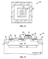
- FIG. 14 is a top view through line 14 - 14 of FIG. 6 ;
- FIG. 15 is a cross-sectional view through an exemplary first type of ESD shunt device according to embodiments of the present invention.
- FIG. 16 is a cross-sectional view through an exemplary second type of ESD shunt device according to embodiments of the present invention.
- FIG. 17 is a cross-sectional view through an exemplary third type of ESD shunt device according to embodiments of the present invention.
- FIG. 18 is a cross-sectional view through an exemplary LDMOS and an exemplary ESD diode during a first simultaneous ion implantation step according to embodiments of the present invention
- FIG. 19 is a cross-sectional view through an exemplary PFET and the exemplary ESD diode of FIG. 18 during a second simultaneous ion implantation step according to embodiments of the present invention.
- FIG. 20 is a schematic circuit diagram of an exemplary integrated circuit using PFETS, NFETS, LDMOSs and ESD diodes and/or ESD shunt devices according to embodiments of the present invention.
- Doped (or diffused) regions of semiconductor substrates are formed by ion implantation of a dopant species (e.g., phosphorus, arsenic, boron) into a semiconductor body followed by annealing (e.g., to at least several hundred degrees centigrade) to activate the dopant species.
- a dopant species e.g., phosphorus, arsenic, boron
- annealing e.g., to at least several hundred degrees centigrade
- a patterned photoresist layers are used to define which regions of an integrated circuit chip will receive a particular ion implantation.
- CMOS complementary metal-oxide-silicon
- LDMOS lateral double diffused field effect transistor
- ESD protection devices include ESD diodes and ESD shunt devices where all three types of devices, CMOS FETs, LDMOS and diodes and/or shunt devices are fabricated on the same integrated circuit chip.
- CMOS devices include P-channel FETs (PFETs) and n-channel FETs (NFETs).
- LDMOS is a high-power (IV) device compared to an NFET or PFET used in CMOS logic, which may be considered low-power devices.
- LDMOS has a higher source to drain breakdown voltages, can carry higher currents and can operate at higher voltage levels than CMOS logic PFETs and NFETs.
- the CMOS logic PFETs and NFETs, LDMOS, and ESD diodes and/or ESD shunt devices are fabricated in the same substrate and utilize a same dielectric trench isolation.
- High-power devices (also known as high-voltage, high-power or high-voltage power devices) operate at a voltage greater than a low-power device.
- High-power device applications operate at, for example, 120 V, 50 V, 45 V, 25 V, 20 V, 20 V, 12 V, and 5V.
- LDMOS are high power-devices. LDMOS are used in both the linear and saturated regime for power applications. LDMOS can operate, for example, at 120 V, 45 V, 25 V, 20 V, and 15 V. LDMOS also find use the lower voltage range between 6.5 to 3.3 V. In one example, a high-power device operates at a voltage about 5 volts or greater and low-power device operates at a voltage of about 1.8 volts or less.
- EOS electrical overstress
- ESD electrical overstress
- LDMOS low-voltage CMOS
- latchup is also a significant concern. Latchup can occur due to interaction between the LDMOS and the low voltage CMOS PFETs and NFETs which are integrated on the same semiconductor chip. As a result, solutions to provide EOS and ESD robustness and latchup insensitivity is desired.
- FIG. 1 is a pictorial top view of an integrated circuit including CMOS FETs, LDMOSs and ESD devices according to embodiments of the present invention.
- an integrated circuit chip includes an exemplary PFET and an exemplary NFET, an LDMOS 105 , an ESD diode 110 and/or an ESD shunt device 115 . Both ESD diode 110 and ESD shunt device 115 need not be present. While only one PFET 95 , one NFET 100 , one LDMOS 105 , one ESD diode 110 and one ESD shunt device 115 are illustrated in FIG. 1 , there may be multiple instances of each type of device.
- PFETs 95 and NFETs 105 may be wired to form CMOS logic circuits.
- LDMOS 105 may be included in power supply circuits.
- ESD diodes 110 may be included in ESD protection circuits.
- ESD shunt devices 115 may be included in ESD protection circuits.
- combinations of ESD diodes 110 and ESD shunt devices 115 may be included in ESD protection circuits.
- FIG. 2 is a cross-sectional view through an exemplary PFET according to embodiments of the present invention.
- a PFET 120 includes source/drains (S/Ds) 125 A and 125 B formed in an N-well 135 formed in a substrate 140 .
- Substrate 140 is doped P-type.
- a gate electrode 145 A is separated from source/drains 125 A and 125 B and N-well 135 by a gate dielectric 150 A.
- Optional dielectric sidewall spacers 155 A are form on the sidewalls of gate electrode 145 A.
- PFET 120 is electrically isolated by dielectric trench isolation 160 .
- a metal silicide layer 161 is formed on a top surface of source/drain 125 A.
- a metal silicide layer 162 is formed on a top surface gate electrode 145 A.
- a metal silicide layer 163 is formed on a top surface of source/drain 125 B.
- substrate 140 is, single-crystal silicon.
- substrate 140 is p-doped.
- gate electrode 145 A is polysilicon.
- Source/drains 125 A and 125 B are formed by a P-type source/drain (P S/D) ion implantation which is a P-type ion implantation.
- N-well 135 is formed by an N-well ion implantation, which is an N-type ion implantation.
- FIG. 3 is a cross-sectional view through an exemplary NFET according to embodiments of the present invention.
- an NFET 165 includes source/drains 170 A and 170 B formed in a P-well 175 formed in substrate 140 .
- a gate electrode 145 B is separated from source/drains 170 A and 170 B and P-well 175 by a gate dielectric 150 B.
- Optional dielectric sidewall spacers 155 B are form on the sidewalls of gate electrode 145 B.
- NFET 165 is electrically isolated by dielectric trench isolation 160 .
- a metal silicide layer 176 is formed on a top surface of source/drain 170 A.
- a metal silicide layer 177 is formed on a top surface gate electrode 145 B.
- a metal silicide layer 178 is formed on a top surface of source/drain 170 B.
- gate electrode 145 B is polysilicon.
- Source/drains 170 A and 170 B are formed by a N-type source/drain (N-S/D) ion implantation which is an N-type ion implantation.
- P-well 175 is formed by a P-well ion implantation, which is a P-type ion implantation.
- N-well and P-well ion implantations are performed first followed by the source/drain ion implantations.
- An exemplary ion implantation order for CMOS device fabrication would be N-well ion implantation, P-well ion implantation, N S/D ion implantation, P S/D ion implantation.
- FIG. 4 is a cross-sectional view through an exemplary first type of LDMOS according to embodiments of the present invention.
- a LDMOS 180 includes a P-type body contact (P+BC) 185 and an N-type source (N+S) 190 formed in and contained in a P-body 195 and an N-type drain (N+D) 200 formed in and contained in an N-body 205 .
- N-tub 210 is formed in substrate 140 .
- P-body 195 and B-body 205 are formed in an N-tub 210 , which is bounded by an N-well 215 and trench isolation 160 .
- P-body 195 and N-body 205 extend under a gate electrode 145 C.
- N-tub 210 intervenes between P-body 195 and N-body 205 under gate electrode 145 C.
- N-type source 190 intervenes between P-type body contact 185 and a region of P-body 195 that extends under gate electrode 145 C.
- Gate electrode 145 C is separated from N-type source 190 , P-body 195 , N-tub 210 and N-body 205 by a gate dielectric 150 C.
- P-type body contact 185 and N-type drain 200 do not extend under gate electrode 145 C.
- a region of dielectric trench isolation surrounds the sidewalls of N-type drain 200 .
- a metal silicide layer 216 is formed on top surfaces of P-type body contact 185 and N-type source 190 .
- a metal silicide layer 217 is formed on a top surface of gate electrode 145 C.
- a metal silicide layer 218 is formed on a top surface of N-type drain 200 .
- P-type body contact 185 is formed by the P S/D ion implantation.
- N-type source 190 and N-type drain 200 are formed by the N S/D ion implantation.
- N-well 215 is formed by the N-well ion implantation.
- P-body 195 is formed by a P-body ion implantation, which is a P-type ion implantation.
- N-body 205 is formed by a N-body ion implantation, which is an N-type ion implantation.
- N-tub 210 is formed by a N-tub ion implantation, which is an N-type ion implantation.
- LDMOS 180 An exemplary ion implantation order for LDMOS 180 would be N-tub ion implantation, N-well ion implantation, P-well ion implantation, N-body ion implantation, P-body ion implantation, N S/D ion implantation, P S/D ion implantation.
- the fabrication of LDMOS 180 utilizes the N-well, N S/D and P S/D ion implantations used to fabricate NFETs and PFETs.
- FIG. 5 is a cross-sectional view through an exemplary second type of LDMOS according to embodiments of the present invention.
- a LDMOS 220 includes a P-type body contact 225 and an N-type source 230 formed in and contained in a P-body 235 .
- LDMOS 220 also includes an N-type drain contact 245 formed in and contained in an N-type drain 240 .
- N-type drain 240 is also formed in and contained in P-body 235 .
- P-body 235 is formed in an N-tub 250 , which is bounded, by an N-well 255 and trench isolation 160 .
- N-type source 230 and N-type drain 240 extend under a gate electrode 145 D.
- Gate electrode 145 D is separated from N-type source 230 , P-body 235 and N-type drain 240 by a gate dielectric 150 D.
- P-type body contact 185 and N-type drain contact 245 do not extend under gate electrode 145 D.
- a metal silicide layer 256 is formed on top surfaces of P-type body contact 225 and N-type source 230 .
- a metal silicide layer 257 is formed on a top surface of gate electrode 145 D.
- a metal silicide layer 258 is formed on a top surface of N-type drain contact 245 .
- P-type body contact 225 is formed by the P S/D ion implantation.
- N-type source 230 and N-type drain contact 245 are formed by the N S/D ion implantation.
- N-well 255 is formed by the N-well ion implantation.
- P-body 235 is formed by the P-body ion implantation.
- N-tub 210 is formed by the N-tub ion implantation.
- N-type drain is formed by a second N-type source (SN) ion implantation, which is an N-type ion implantation.
- An exemplary ion implantation order for LDMOS 220 would be N-tub, N-well, P-well, N-body, SN, N S/D, P S/D.
- the fabrication of LDMOS 220 utilizes the N-well, N S/D and P S/D ion implantations used to fabricate NFETs and PFETs.
- An overall exemplary ion implantation order would be N-tub, N-well, P-well, N-body, P-body, SN, N S/D, P S/D wherein the order of N-well and P-well may be reversed, the order of N S/D and P S/D may be reversed, and the order of N-body and P-body may be reversed.
- N-tub, N-well, P-well, N-body, P-body, SN, N S/D and P S/D ion implantations extend from the top surface of the substrate into the substrate, so some regions actually see more than on ion implantations.
- P-body 235 includes N-type dopant from the N-tub ion implantation and P-type dopant from the P-body ion implantation, but the net doping is P-type.
- the boundaries illustrated in the drawings are PN junction or differences in concentration between regions of the same doping concentration. It should also be realized that the doping concentration is not necessarily uniform through any particular doped region but may vary with distance from the top surface of the substrate.
- the eight ion implantations in order of decreasing ion implantation dose (atm/cm 2 ) (or decreasing concentration (atm/cm 3 ) in the substrate) is N S/D and P S/D, SN, N-well and P-well, N-body and P-body, and N-tub wherein N-well and P-well may be ion implanted at different doses, N S/D and P S/D may be ion implanted at different doses, and N-body and P-body may be ion implanted at different doses.
- the eight ion implantations in order of increasing energy (KeV) or increasing depth into the substrate) is N S/D and P S/D, SN, N-body and P-body, N-well and P-well, N-tub wherein N-well and P-well may be ion implanted at different energies, N S/D and P S/D may be may be ion implanted at different energies, and the order of N-body and P-body may be ion implanted at different energies.
- N-well, P-well, P-body, N-body and N-tub ion implantations are performed prior to formation dielectric trench isolation and P S/D, N S/D and SN ion implantations are performed after formation of dielectric trench isolation.
- the ESD diodes and ESD shunt devices described infra are fabricated using one or more of these eight ion implantations. In one example, the ESD diodes and ESD shunt devices described infra are fabricated using four or more of these eight ion implantations and no other ion implantations. In one example, the ESD diodes and ESD shunt devices described infra, are fabricated using at least one ion implantation used to fabricate PFETs or NFETs and at least one ion implantation used to fabricate LDMOSs.
- FIG. 6 is a cross-sectional view through an exemplary first type of ESD diode according to embodiments of the present invention.
- an ESD diode 260 includes an N-type cathode 265 and a P-type anode 270 in an N-body 275 .
- N-body 275 is formed in substrate 140 .
- N-type cathode 265 is separated from P-type anode 270 by dielectric trench isolation 160 .
- An N-well 280 extends from the bottom of N-body 275 into substrate 140 .
- a metal silicide layer 281 is formed on a top surface of N-type cathode 265 and a metal silicide layer 282 is formed on a top surface of P-type anode 270 .
- N-type cathode 265 is formed by the third (N S/D) ion implantation.
- P-type anode 270 is formed by the first (P S/D) ion implantation.
- N-body 275 is formed by the sixth (N-body) ion implantation.
- N-well 280 is formed by the second (N-well) ion implantation.
- ESD diode 260 utilizes the N-well, N S/D and P S/D ion implantations used to fabricate NFETs and PFETs and the N-body ion implantation used to fabricate LDMOSs.
- FIG. 7 is a cross-sectional view through an exemplary second type of ESD diode according to embodiments of the present invention.
- an ESD diode 285 includes an N-type cathode 290 and a P-type anode 295 in an N-body 300 .
- N-type cathode 290 is separated from P-type anode 295 by dielectric trench isolation 160 .
- N-body 300 is formed in an N-tub 310 , which is formed in substrate 140 .
- An N-well 310 extends from the bottom of N-body 300 into N-tub 305 , but not past the bottom of the N-tub.
- a metal silicide layer 311 is formed on a top surface of N-type cathode 290 and a metal silicide layer 312 is formed on a top surface of P-type anode 295 .
- N-type cathode 290 is formed by the N S/D ion implantation.
- P-type anode 295 is formed by the P S/D ion implantation.
- N-body 300 is formed by the N-body ion implantation.
- N-well 310 is formed by the N-well ion implantation.
- N-tub 305 is formed by the N-tub ion implantation.
- ESD diode 285 utilizes the N-well, N S/D and P S/D ion implantations used to fabricate NFETs and PFETs and the N-body and N-tub ion implantations used to fabricate LDMOSs.
- FIG. 8 is a cross-sectional view through an exemplary third type of ESD diode according to embodiments of the present invention.
- an ESD diode 315 includes an N-type cathode 320 and a P-type anode 325 in an N-well 335 A.
- N-well 335 A is formed in substrate 140 .
- An N-type buried region 330 is formed between N-type cathode 320 and N-well 335 A.
- N-type cathode 320 and N-type buried region 330 are separated from P-type anode 325 by dielectric trench isolation 160 .
- a metal silicide layer 336 is formed on a top surface of N-type cathode 320 and a metal silicide layer 337 is formed on a top surface of P-type anode 325 .
- N-type cathode 320 is formed by the third (N S/D) ion implantation.
- P-type anode 325 is formed by the P S/D ion implantation.
- N-well 335 A is formed by the N-well ion implantation.
- N-type buried region 330 is formed by the SN ion implantation.
- ESD diode 315 utilizes the N-well, N S/D and P S/D ion implantations used to fabricate NFETs and PFETs and the SN ion implantation used to fabricate LDMOSs.
- FIG. 9 is a cross-sectional view through an exemplary fourth type of ESD diode according to embodiments of the present invention.
- an ESD diode 340 includes an N-type cathode 345 and a P-type anode 350 in an N-well 335 B.
- N-well 335 B is formed in substrate 140 .
- An N-type buried region 355 is formed between N-type cathode 345 and N-well 335 B.
- N-type cathode 345 and N-type buried region 355 are separated from P-type anode 350 by dielectric trench isolation 160 .
- a metal silicide layer 356 is formed on a top surface of N-type cathode 355 and a metal silicide layer 357 is formed on a top surface of P-type anode 350 .
- N-type cathode 345 is formed by the N S/D ion implantation.
- P-type anode 350 is formed by the first (P S/D) ion implantation.
- P-well 335 B is formed by the P-well ion implantation.
- N-type buried region 355 is formed by the SN ion implantation.
- ESD diode 340 utilizes the P-well, N S/D and P S/D ion implantations used to fabricate NFETs and PFETs and the SN ion implantation used to fabricate LDMOSs.
- FIG. 10 is a cross-sectional view through an exemplary fifth type of ESD diode according to embodiments of the present invention.
- an ESD diode 360 includes an N-type cathode 365 and a P-type anode 370 in an N-well 380 .
- N-well 380 is formed in an N-tub 380 , which is formed in substrate 140 .
- An N-type buried region 375 is formed between N-type cathode 365 and N-well 380 .
- N-type cathode 365 and N-type buried region 375 are separated from P-type anode 380 by dielectric trench isolation 160 .
- a metal silicide layer 386 is formed on a top surface of N-type cathode 365 and a metal silicide layer 387 is formed on a top surface of P-type anode 370 .
- N-type cathode 365 is formed by the N S/D ion implantation.
- P-type anode 380 is formed by the P S/D ion implantation.
- N-well 380 is formed by the N-well ion implantation.
- N-type buried region 375 is formed by the SN ion implantation.
- N-tub 385 is formed by the N-tub ion implantation.
- ESD diode 360 utilizes the N-well, N S/D and P S/D ion implantations used to fabricate NFETs and PFETs and the SN and N-tub ion implantations used to fabricate LDMOSs.
- FIG. 11 is a cross-sectional view through an exemplary sixth type of ESD diode according to embodiments of the present invention.
- an ESD diode 390 includes an N-type cathode 395 and a P-type anode 400 in a P-body 405 .
- N-type cathode 395 is separated from P-type anode 400 by dielectric trench isolation 160 .
- P-body 405 is formed in a P-well 410 , which is formed in substrate 140 .
- a metal silicide layer 411 is formed on a top surface of N-type cathode 395 and a metal silicide layer 412 is formed on a top surface of P-type anode 400 .
- N-type cathode 395 is formed by the third (N S/D) ion implantation.
- P-type anode 400 is formed by the P S/D ion implantation.
- P-body 300 is formed by the P-body ion implantation.
- P-well 410 is formed by the P-well ion implantation.
- ESD diode 390 utilizes the P-well, N S/D and P S/D ion implantations used to fabricate NFETs and PFETs and the P-body ion implantation used to fabricate LDMOSs.
- FIG. 12 is a cross-sectional view through an exemplary seventh type of ESD diode according to embodiments of the present invention.
- an ESD diode 415 includes an N-type cathode 420 and a P-type anode 425 in a P-body 430 .
- An N-type buried region 445 is formed between N-type cathode 445 and P-body 460 .
- N-type cathode 420 and N-type buried region 455 are separated from P-type anode 425 by dielectric trench isolation 160 .
- P-body 430 is formed in an N-tub 432 , which is formed in substrate 140 .
- a P-well 435 extends from the bottom of P-body 430 into N-tub 432 but not past a bottom of the N-tub.
- a metal silicide layer 436 is formed on a top surface of N-type cathode 420 and a metal silicide layer 437 is formed on a top surface of P-type anode 425 .
- N-type cathode 420 is formed by the N S/D ion implantation.
- P-type anode 425 is formed by the P S/D ion implantation.
- P-body 430 is formed by the P-body ion implantation.
- P-well 435 is formed by the P-well ion implantation.
- N-tub 432 is formed by the N-tub ion implantation.
- ESD diode 415 utilizes the P-well, N S/D and P S/D ion implantations used to fabricate NFETs and PFETs and the P-body and N-tub ion implantations used to fabricate LDMOSs.
- FIG. 13 is a cross-sectional view through an exemplary eighth type of ESD diode according to embodiments of the present invention.
- an ESD diode 440 includes an N-type cathode 445 and a P-type anode 450 in a P-body 460 .
- a N-type buried region 455 intervenes between N-type cathode 445 and P-body 460 .
- N-type cathode 445 and buried N-type region 455 are separated from P-type anode 450 by dielectric trench isolation 160 .
- P-body 460 is formed in an N-tub 462 , which is formed in substrate 140 .
- a P-well 465 extends from the bottom of P-body 460 into N-tub 462 but not past a bottom of the N-tub.
- a metal silicide layer 467 is formed on a top surface of N-type cathode 445 and a metal silicide layer 468 is formed on a top surface of P-type anode 450 .
- N-type cathode 445 is formed by the N S/D ion implantation.
- P-type anode 450 is formed by the P S/D ion implantation.
- P-body 460 is formed by the P-body ion implantation.
- P-well 465 is formed by the P-well ion implantation.
- N-tub 462 is formed by the N-tub ion implantation.
- Buried region 455 is formed by the SN ion implantation.
- the fabrication of ESD diode 440 utilizes the P-well, N S/D and P S/D ion implantations used to fabricate NFETs and PFETs and the P-body, N-tub ion and SN ion implantations used to fabricate LDMOSs.
- FIG. 14 is a top view through line 14 - 14 of FIG. 6 .
- ESD diode 260 comprises a ring shaped N-type cathode 265 surrounding a perimeter of P-type cathode 270 with a ring of trench dielectric isolation 160 intervening between N-type cathode 265 and P-type anode 270 .
- This ring-shaped diode structure is exemplary of all seven of the ESD diodes described supra.
- the ESD diodes of the embodiments of the present invention are not limited to this particular geometric layout and other layers layouts such as a stripe of anode between two stripes of cathode may also be used.
- FIG. 15 is a cross-sectional view through an exemplary first type of ESD shunt device according to embodiments of the present invention.
- ESD shunt devices according to embodiments of the present inventions are a type of FET.
- an ESD shunt device 470 includes a P-type body contact 475 , an N-type source 480 and an N-type drain 485 formed in substrate 140 .
- a P-well 495 extends from a bottom of P-body 490 into substrate 140 .
- N-type source 480 and N-type drain 485 extend under a gate electrode 145 E.
- a region of P-body 490 intervenes between N-type source 480 and N-type drain 485 under gate electrode 145 E.
- Gate electrode 145 E is separated from N-type source 480 , P-body 490 and N-type drain 485 by a gate dielectric 150 E.
- P-type body contact 475 is isolated from N-type source 480 by a region of locally oxidized silicon (LOCOS) 500 .
- a metal silicide layer 501 is formed on top surfaces of P-type body contact 475 .
- a metal silicide layer 502 is formed on a top surface of N-type source 480 .
- a metal silicide layer 503 is formed on a top surface of gate electrode 145 E.
- a metal silicide layer 504 is formed on a top surface of N-type drain 485 .
- P-type body contact 475 is formed by the P S/D ion implantation.
- N-type source 480 and N-type drain 485 are formed by the N S/D ion implantation.
- P-well 490 is formed by the P-well ion implantation.
- P-body 495 is formed by the P-body ion implantation.
- FIG. 16 is a cross-sectional view through an exemplary second type of ESD shunt device according to embodiments of the present invention.
- an ESD shunt device 505 includes an N-type body contact 510 , a P-type source 515 and a P-type drain 520 formed in and contained in an N-body 525 .
- N-body 525 is formed in a substrate 140 .
- a region of N-well 530 extends from a bottom of N-body 525 into substrate 530 .
- P-type source 515 and P-type drain 520 extend under a gate electrode 145 F.
- a region of N-body 525 intervenes between P-type source 515 and P-type drain 520 under gate electrode 145 F.
- Gate electrode 145 F is separated from P-type source 515 , N-body 525 and P-type drain 520 by a gate dielectric 150 F.
- N-type body contact 510 is isolated from P-type source 515 by a region of LOCOS 535 .
- a metal silicide layer 531 is formed on top surfaces of N-type body contact 510 .
- a metal silicide layer 532 is formed on a top surface of P-type source 515 .
- a metal silicide layer 533 is formed on a top surface of gate electrode 145 F.
- a metal silicide layer 534 is formed on a top surface of P-type drain 520 .
- N-type body contact 510 is formed by the N S/D ion implantation.
- P-type source 515 and P-type drain 520 are formed by the P S/D ion implantation.
- N-well 530 is formed by the N-well ion implantation.
- N-body 525 is formed by the N-body ion implantation.
- FIG. 17 is a cross-sectional view through an exemplary third type of ESD shunt device according to embodiments of the present invention.
- an ESD shunt device 540 includes an N-type body contact 545 , a P-type source 550 and a P-type drain 555 formed in and contained in an N-body 560 .
- N-body 560 is formed in and contained in an N-tub 565 formed in substrate 140 .
- a region of N-well 570 extends from a bottom of N-body 560 into N-tub 565 but not past a bottom of the N-tub.
- P-type source 550 and P-type drain 555 extend under a gate electrode 145 G.
- Gate electrode 145 G is separated from P-type source 550 , N-body 560 and P-type drain 555 by a gate dielectric 150 G.
- N-type body contact 545 and buried N-type region 575 are isolated from P-type source 550 by a region of dielectric trench isolation 160 .
- a metal silicide layer 576 is formed on top surfaces of N-type body contact 545 .
- a metal silicide layer 577 is formed on a top surface of P-type source 550 .
- a metal silicide layer 578 is formed on a top surface of gate electrode 145 G.
- a metal silicide layer 579 is formed on a top surface of P-type drain 555 .
- N-type body contact 545 is formed by the N S/D ion implantation.
- P-type source 550 and P-type drain 555 are formed by the P S/D ion implantation.
- N-well 570 is formed by the N-well ion implantation.
- N-body 560 is formed by the N-body ion implantation.
- N-tub 565 is formed by the N-tub ion implantation.
- Buried N-type region 575 is formed by the SN ion implantation.
- ESD shunt device 540 utilizes the N-well, N S/D and P S/D ion implantations used to fabricate NFETs and PFETs and the N-body, N-tub and SN ion implantations used to fabricate LDMOSs.
- Table I summarizes the ion implantation steps used to fabricate CMOS FETS, LDMOSs and ESD diodes and ESD shunt devices according to embodiments of the present invention described supra.
- FIG. 18 is a cross-sectional view through an exemplary LDMOS and an exemplary ESD diode during a first simultaneous ion implantation step according to embodiments of the present invention.
- an ESD diode 600 and LDMOS 605 are being fabricated in a substrate 610 .
- a patterned photoresist layer 615 has been form on substrate 610 and an ion implant of dopant species X performed to form a P-body in LDMOS 605 and an P-body 625 in ESD diode 600 .
- Photoresist layer 615 is removed after the ion implantation.
- Dopant species X is a P-type dopant (e.g., boron).
- patterned photoresist layer 615 may be formed on a dielectric hardmask layer and not directly on the top surface of substrate 610 .
- FIG. 19 is a cross-sectional view through an exemplary PFET and the exemplary ESD diode of FIG. 18 during a first simultaneous ion implantation step according to embodiments of the present invention.
- a PFET 630 and ESD diode 605 during fabrication are shown.
- dielectric trench isolation 635 has been formed in both PFET 630 and ESD diode 605 .
- a gate dielectric 645 and gate electrode 650 have been formed in PFET 630 .
- a patterned photoresist layer 655 is formed over substrate 610 and an ion implant of dopant species Y performed to form a P-type source/drain in PFET 630 , a doped gate region 670 in gate electrode 650 , and a P-type anode 675 in ESD diode 600 .
- Photoresist layer 655 is removed after the ion implantation.
- Dopant species Y is a P-type dopant (e.g., boron).
- FIG. 20 is a schematic circuit diagram of an exemplary integrated circuit using PFETS, NFETS, LDMOSs and ESD diodes and/or ESD shunt devices according to embodiments of the present invention.
- an integrated circuit chip 700 includes CMOS logic 705 comprising PFETs and NFETs, a power distribution network 710 comprising LDMOSs (used for example, as switches, voltage regulators and/or DC to DC converters) and an ESD protection circuit 715 comprising ESD diodes and/or ESD shunt devices.
- Power distribution network is connected to power supply pads 725 and distributes power to CMOS logic 705 and ESD protection circuit 715 .
- ESD protection circuit 715 is connected between CMOS logic 705 and I/O pads 730 .
- the ESD diodes and/or ESD shunt devices (i) share at least one ion implantation process with either the PFETs or NFETs or (ii) share at least one ion implantation process with the LDMOSs or (iii) share at least one ion implantation process with either the PFETs or NFETs and share at least one ion implantation process with the LDMOSs.
- the embodiments of the present invention provide a method for fabricating ESD devices simultaneously with LDMOSs and CMOS FETs using LDMOS and MOSFET ion implantations and without the use of dedicated ion implantations for the ESD devices.
Abstract
Description
| TABLE I | |||
| CMOS FET I/I Processes | LDMOS I/I Processes | ||
| I/I | P S/D | N S/D | N-Well | P-Well | N-Body | SN | P-Body | N-Tub |
| PFET | X | X | ||||||
| NFET | X | X | ||||||
| LDMOS #1 | X | X | X | X | X | X | ||
| LDMOS #2 | X | X | X | X | X | x | ||
| ESD DIODE #1 | X | X | X | X | ||||
| ESD DIODE #2 | X | X | X | X | X | |||
| ESD DIODE #3 | X | X | X | X | ||||
| ESD DIODE #4 | X | X | X | X | ||||
| ESD DIODE #5 | X | X | X | X | X | |||
| ESD DIODE #6 | X | X | X | X | ||||
| ESD DIODE #7 | X | X | X | X | X | |||
| ESD DIODE #8 | X | X | X | X | X | X | ||
| ESD SHUNT #1 | X | X | X | X | ||||
| ESD SHUNT #2 | X | X | X | X | ||||
| ESD SHUNT #3 | X | X | X | X | X | |||
Claims (11)
Priority Applications (1)
| Application Number | Priority Date | Filing Date | Title |
|---|---|---|---|
| US12/541,484 US8088656B2 (en) | 2009-08-14 | 2009-08-14 | Fabricating ESD devices using MOSFET and LDMOS |
Applications Claiming Priority (1)
| Application Number | Priority Date | Filing Date | Title |
|---|---|---|---|
| US12/541,484 US8088656B2 (en) | 2009-08-14 | 2009-08-14 | Fabricating ESD devices using MOSFET and LDMOS |
Publications (2)
| Publication Number | Publication Date |
|---|---|
| US20110039378A1 US20110039378A1 (en) | 2011-02-17 |
| US8088656B2 true US8088656B2 (en) | 2012-01-03 |
Family
ID=43588820
Family Applications (1)
| Application Number | Title | Priority Date | Filing Date |
|---|---|---|---|
| US12/541,484 Expired - Fee Related US8088656B2 (en) | 2009-08-14 | 2009-08-14 | Fabricating ESD devices using MOSFET and LDMOS |
Country Status (1)
| Country | Link |
|---|---|
| US (1) | US8088656B2 (en) |
Cited By (2)
| Publication number | Priority date | Publication date | Assignee | Title |
|---|---|---|---|---|
| US10084079B2 (en) | 2015-06-16 | 2018-09-25 | Samsung Electronics Co., Ltd. | Semiconductor device having a drift region with non-uniform impurity concentration profile |
| US10453836B2 (en) * | 2017-08-17 | 2019-10-22 | Globalfoundries Singapore Pte. Ltd. | High holding high voltage (HHHV) FET for ESD protection with modified source and method for producing the same |
Families Citing this family (10)
| Publication number | Priority date | Publication date | Assignee | Title |
|---|---|---|---|---|
| US8981495B2 (en) | 2010-02-08 | 2015-03-17 | Taiwan Semiconductor Manufacturing Company, Ltd. | Laterally diffused metal oxide semiconductor transistor with partially unsilicided source/drain |
| US8759913B2 (en) * | 2012-05-15 | 2014-06-24 | Richtek Technology Corporation | Double diffused drain metal oxide semiconductor device and manufacturing method thereof |
| KR101467703B1 (en) * | 2013-10-10 | 2014-12-02 | 매그나칩 반도체 유한회사 | semiconductor device and manufacturing method thereof |
| CN104701356B (en) * | 2013-12-06 | 2018-01-12 | 无锡华润上华科技有限公司 | Semiconductor devices and preparation method thereof |
| US9559097B2 (en) * | 2014-10-06 | 2017-01-31 | Nxp Usa, Inc. | Semiconductor device with non-isolated power transistor with integrated diode protection |
| CN106206561B (en) * | 2015-04-29 | 2019-05-10 | 无锡华润上华科技有限公司 | The electrostatic protection device of LDMOS SCR structure |
| TWI621273B (en) * | 2017-04-27 | 2018-04-11 | 立錡科技股份有限公司 | High Voltage Depletion Mode MOS Device with Adjustable Threshold Voltage and Manufacturing Method Thereof |
| KR102299662B1 (en) | 2017-07-13 | 2021-09-07 | 매그나칩 반도체 유한회사 | Semiconductor Device and Method for Fabricating the Same |
| CN111799257B (en) * | 2020-07-17 | 2023-05-12 | 上海华力微电子有限公司 | Protection ring for improving negative current latch-up prevention capability of high-voltage integrated circuit and implementation method |
| US11804482B2 (en) * | 2020-09-29 | 2023-10-31 | Taiwan Semiconductor Manufacturing Company Ltd. | Transistor drain design for ESD protection and manufacturing method thereof |
Citations (14)
| Publication number | Priority date | Publication date | Assignee | Title |
|---|---|---|---|---|
| US5346835A (en) | 1992-07-06 | 1994-09-13 | Texas Instruments Incorporated | Triple diffused lateral resurf insulated gate field effect transistor compatible with process and method |
| US5578860A (en) * | 1995-05-01 | 1996-11-26 | Motorola, Inc. | Monolithic high frequency integrated circuit structure having a grounded source configuration |
| US5591661A (en) * | 1992-04-07 | 1997-01-07 | Shiota; Philip | Method for fabricating devices for electrostatic discharge protection and voltage references, and the resulting structures |
| US6576961B1 (en) * | 2002-04-24 | 2003-06-10 | Texas Instruments Incorporated | Substrate resistance ring |
| US20040251492A1 (en) | 2003-06-13 | 2004-12-16 | John Lin | LDMOS transistors and methods for making the same |
| US6855985B2 (en) | 2002-09-29 | 2005-02-15 | Advanced Analogic Technologies, Inc. | Modular bipolar-CMOS-DMOS analog integrated circuit & power transistor technology |
| US20050148124A1 (en) * | 2003-05-14 | 2005-07-07 | Jun Cai | ESD protection for semiconductor products |
| US20050242399A1 (en) * | 2004-04-28 | 2005-11-03 | Taiwan Semiconductor Manufacturing Co., Ltd. | MOSFET with electrostatic discharge protection structure and method of fabrication |
| US20060197149A1 (en) | 2005-03-07 | 2006-09-07 | Keiji Fujimoto | Semiconductor device and fabrication process thereof, and application thereof |
| US7125777B2 (en) | 2004-07-15 | 2006-10-24 | Fairchild Semiconductor Corporation | Asymmetric hetero-doped high-voltage MOSFET (AH2MOS) |
| US20060286735A1 (en) | 2004-08-11 | 2006-12-21 | You-Kuo Wu | Integrated circuit transistor insulating region fabrication method |
| US7220633B2 (en) | 2003-11-13 | 2007-05-22 | Volterra Semiconductor Corporation | Method of fabricating a lateral double-diffused MOSFET |
| US20070207600A1 (en) * | 2006-03-02 | 2007-09-06 | Volterra Semiconductor Corporation | Lateral Double-Diffused Mosfet (LDMOS) Transistor and a Method of Fabricating the Same |
| US7718494B2 (en) * | 2007-04-09 | 2010-05-18 | Taiwan Semiconductor Manufacturing Company, Ltd. | Method for forming high-drain-voltage tolerance MOSFET transistor in a CMOS process flow with double well dose approach |
-
2009
- 2009-08-14 US US12/541,484 patent/US8088656B2/en not_active Expired - Fee Related
Patent Citations (15)
| Publication number | Priority date | Publication date | Assignee | Title |
|---|---|---|---|---|
| US5591661A (en) * | 1992-04-07 | 1997-01-07 | Shiota; Philip | Method for fabricating devices for electrostatic discharge protection and voltage references, and the resulting structures |
| US5346835A (en) | 1992-07-06 | 1994-09-13 | Texas Instruments Incorporated | Triple diffused lateral resurf insulated gate field effect transistor compatible with process and method |
| US5578860A (en) * | 1995-05-01 | 1996-11-26 | Motorola, Inc. | Monolithic high frequency integrated circuit structure having a grounded source configuration |
| US6576961B1 (en) * | 2002-04-24 | 2003-06-10 | Texas Instruments Incorporated | Substrate resistance ring |
| US7211863B2 (en) | 2002-09-29 | 2007-05-01 | Advanced Analogic Technologies, Inc. | Modular bipolar-CMOS-DMOS analog integrated circuit and power transistor technology |
| US6855985B2 (en) | 2002-09-29 | 2005-02-15 | Advanced Analogic Technologies, Inc. | Modular bipolar-CMOS-DMOS analog integrated circuit & power transistor technology |
| US20050148124A1 (en) * | 2003-05-14 | 2005-07-07 | Jun Cai | ESD protection for semiconductor products |
| US20040251492A1 (en) | 2003-06-13 | 2004-12-16 | John Lin | LDMOS transistors and methods for making the same |
| US7220633B2 (en) | 2003-11-13 | 2007-05-22 | Volterra Semiconductor Corporation | Method of fabricating a lateral double-diffused MOSFET |
| US20050242399A1 (en) * | 2004-04-28 | 2005-11-03 | Taiwan Semiconductor Manufacturing Co., Ltd. | MOSFET with electrostatic discharge protection structure and method of fabrication |
| US7125777B2 (en) | 2004-07-15 | 2006-10-24 | Fairchild Semiconductor Corporation | Asymmetric hetero-doped high-voltage MOSFET (AH2MOS) |
| US20060286735A1 (en) | 2004-08-11 | 2006-12-21 | You-Kuo Wu | Integrated circuit transistor insulating region fabrication method |
| US20060197149A1 (en) | 2005-03-07 | 2006-09-07 | Keiji Fujimoto | Semiconductor device and fabrication process thereof, and application thereof |
| US20070207600A1 (en) * | 2006-03-02 | 2007-09-06 | Volterra Semiconductor Corporation | Lateral Double-Diffused Mosfet (LDMOS) Transistor and a Method of Fabricating the Same |
| US7718494B2 (en) * | 2007-04-09 | 2010-05-18 | Taiwan Semiconductor Manufacturing Company, Ltd. | Method for forming high-drain-voltage tolerance MOSFET transistor in a CMOS process flow with double well dose approach |
Cited By (3)
| Publication number | Priority date | Publication date | Assignee | Title |
|---|---|---|---|---|
| US10084079B2 (en) | 2015-06-16 | 2018-09-25 | Samsung Electronics Co., Ltd. | Semiconductor device having a drift region with non-uniform impurity concentration profile |
| US10453836B2 (en) * | 2017-08-17 | 2019-10-22 | Globalfoundries Singapore Pte. Ltd. | High holding high voltage (HHHV) FET for ESD protection with modified source and method for producing the same |
| US11257808B2 (en) | 2017-08-17 | 2022-02-22 | Globalfoundries Singapore Pte. Ltd. | High holding high voltage (HHHV) FET for ESD protection with modified source and method for producing the same |
Also Published As
| Publication number | Publication date |
|---|---|
| US20110039378A1 (en) | 2011-02-17 |
Similar Documents
| Publication | Publication Date | Title |
|---|---|---|
| US8088656B2 (en) | Fabricating ESD devices using MOSFET and LDMOS | |
| EP1543546B1 (en) | Process for fabricating an isolated field effect transistor in an epi-less substrate | |
| US7372083B2 (en) | Embedded silicon-controlled rectifier (SCR) for HVPMOS ESD protection | |
| US7411271B1 (en) | Complementary metal-oxide-semiconductor field effect transistor | |
| US7358573B2 (en) | Triple-well CMOS devices with increased latch-up immunity and methods of fabricating same | |
| US8026549B2 (en) | LDMOS with N-type isolation ring and method of fabricating the same | |
| US8053843B2 (en) | Integrated electrostatic discharge (ESD) device | |
| US20090020826A1 (en) | Integrated Schottky Diode and Power MOSFET | |
| US20120061761A1 (en) | Semiconductor integrated circuit device and manufacturing method for semiconductor integrated circuit devices | |
| US11152505B2 (en) | Drain extended transistor | |
| US20060065931A1 (en) | ESD protection for high voltage applications | |
| US20200006550A1 (en) | Protection of drain extended transistor field oxide | |
| US8178925B2 (en) | Semiconductor diode structure operation method | |
| US7279767B2 (en) | Semiconductor structure with high-voltage sustaining capability and fabrication method of the same | |
| KR101294115B1 (en) | Semiconductor device and fabrication method therefor | |
| US20120018775A1 (en) | Electrostatic discharge protection device and method for fabricating the same | |
| US8692327B2 (en) | Lateral double diffused metal oxide semiconductor device and method for manufacturing the same | |
| US9087708B2 (en) | IC with floating buried layer ring for isolation of embedded islands | |
| US8283726B2 (en) | System and method for I/O ESD protection with polysilicon regions fabricated by processes for making core transistors | |
| US7955923B1 (en) | I/O ESD protection device for high performance circuits | |
| CN109411466B (en) | High-retention high-voltage FET for ESD protection and method of manufacturing the same | |
| US8828827B2 (en) | Manufacturing method of anti punch-through leakage current metal-oxide-semiconductor transistor | |
| US11257907B2 (en) | High voltage demos transistor with improved threshold voltage matching | |
| US9583564B2 (en) | Isolation structure | |
| JPH0846054A (en) | Semiconductor device |
Legal Events
| Date | Code | Title | Description |
|---|---|---|---|
| AS | Assignment |
Owner name: INTERNATIONAL BUSINESS MACHINES CORPORATION, NEW Y Free format text: ASSIGNMENT OF ASSIGNORS INTEREST;ASSIGNOR:VOLDMAN, STEVEN HOWARD;REEL/FRAME:023102/0043 Effective date: 20090801 |
|
| STCF | Information on status: patent grant |
Free format text: PATENTED CASE |
|
| FPAY | Fee payment |
Year of fee payment: 4 |
|
| SULP | Surcharge for late payment | ||
| AS | Assignment |
Owner name: GLOBALFOUNDRIES U.S. 2 LLC, NEW YORK Free format text: ASSIGNMENT OF ASSIGNORS INTEREST;ASSIGNOR:INTERNATIONAL BUSINESS MACHINES CORPORATION;REEL/FRAME:036550/0001 Effective date: 20150629 |
|
| AS | Assignment |
Owner name: GLOBALFOUNDRIES INC., CAYMAN ISLANDS Free format text: ASSIGNMENT OF ASSIGNORS INTEREST;ASSIGNORS:GLOBALFOUNDRIES U.S. 2 LLC;GLOBALFOUNDRIES U.S. INC.;REEL/FRAME:036779/0001 Effective date: 20150910 |
|
| AS | Assignment |
Owner name: ALSEPHINA INNOVATIONS INC., CANADA Free format text: ASSIGNMENT OF ASSIGNORS INTEREST;ASSIGNOR:GLOBALFOUNDRIES INC.;REEL/FRAME:049612/0211 Effective date: 20181126 |
|
| FEPP | Fee payment procedure |
Free format text: MAINTENANCE FEE REMINDER MAILED (ORIGINAL EVENT CODE: REM.); ENTITY STATUS OF PATENT OWNER: LARGE ENTITY |
|
| LAPS | Lapse for failure to pay maintenance fees |
Free format text: PATENT EXPIRED FOR FAILURE TO PAY MAINTENANCE FEES (ORIGINAL EVENT CODE: EXP.); ENTITY STATUS OF PATENT OWNER: LARGE ENTITY |
|
| STCH | Information on status: patent discontinuation |
Free format text: PATENT EXPIRED DUE TO NONPAYMENT OF MAINTENANCE FEES UNDER 37 CFR 1.362 |
|
| FP | Lapsed due to failure to pay maintenance fee |
Effective date: 20200103 |
|
| AS | Assignment |
Owner name: GLOBALFOUNDRIES INC., CAYMAN ISLANDS Free format text: RELEASE BY SECURED PARTY;ASSIGNOR:WILMINGTON TRUST, NATIONAL ASSOCIATION;REEL/FRAME:054636/0001 Effective date: 20201117 |