US8089285B2 - Implementing tamper resistant integrated circuit chips - Google Patents
Implementing tamper resistant integrated circuit chips Download PDFInfo
- Publication number
- US8089285B2 US8089285B2 US12/396,512 US39651209A US8089285B2 US 8089285 B2 US8089285 B2 US 8089285B2 US 39651209 A US39651209 A US 39651209A US 8089285 B2 US8089285 B2 US 8089285B2
- Authority
- US
- United States
- Prior art keywords
- tamper resistant
- control signal
- functional operation
- chip
- resistant control
- Prior art date
- Legal status (The legal status is an assumption and is not a legal conclusion. Google has not performed a legal analysis and makes no representation as to the accuracy of the status listed.)
- Expired - Fee Related, expires
Links
- 238000013461 design Methods 0.000 claims abstract description 58
- 238000000034 method Methods 0.000 claims abstract description 43
- 239000004065 semiconductor Substances 0.000 claims abstract description 36
- 230000002401 inhibitory effect Effects 0.000 claims abstract description 29
- 238000012360 testing method Methods 0.000 claims description 30
- 238000012938 design process Methods 0.000 claims description 10
- 238000004519 manufacturing process Methods 0.000 claims description 8
- 238000012795 verification Methods 0.000 claims description 3
- 238000012512 characterization method Methods 0.000 claims description 2
- 238000003860 storage Methods 0.000 claims description 2
- 230000003287 optical effect Effects 0.000 description 7
- 230000008569 process Effects 0.000 description 7
- 238000010586 diagram Methods 0.000 description 6
- 230000001066 destructive effect Effects 0.000 description 4
- 238000005516 engineering process Methods 0.000 description 4
- 230000006870 function Effects 0.000 description 4
- 239000000463 material Substances 0.000 description 4
- 239000002184 metal Substances 0.000 description 4
- 239000000758 substrate Substances 0.000 description 4
- 230000001960 triggered effect Effects 0.000 description 4
- 230000007246 mechanism Effects 0.000 description 3
- 238000012544 monitoring process Methods 0.000 description 3
- 238000004458 analytical method Methods 0.000 description 2
- 238000013459 approach Methods 0.000 description 2
- 238000001514 detection method Methods 0.000 description 2
- 238000009792 diffusion process Methods 0.000 description 2
- 230000000694 effects Effects 0.000 description 2
- 230000005669 field effect Effects 0.000 description 2
- 238000012797 qualification Methods 0.000 description 2
- 238000012827 research and development Methods 0.000 description 2
- 229910052710 silicon Inorganic materials 0.000 description 2
- 239000010703 silicon Substances 0.000 description 2
- 102100025654 Endosome-associated-trafficking regulator 1 Human genes 0.000 description 1
- 101001056455 Homo sapiens Endosome-associated-trafficking regulator 1 Proteins 0.000 description 1
- 229910000577 Silicon-germanium Inorganic materials 0.000 description 1
- 239000002253 acid Substances 0.000 description 1
- 230000008859 change Effects 0.000 description 1
- 230000002950 deficient Effects 0.000 description 1
- 238000012407 engineering method Methods 0.000 description 1
- 238000003384 imaging method Methods 0.000 description 1
- 238000010884 ion-beam technique Methods 0.000 description 1
- 150000002500 ions Chemical class 0.000 description 1
- 238000012804 iterative process Methods 0.000 description 1
- 230000015654 memory Effects 0.000 description 1
- 238000003801 milling Methods 0.000 description 1
- 238000004806 packaging method and process Methods 0.000 description 1
- 238000001020 plasma etching Methods 0.000 description 1
- 238000012545 processing Methods 0.000 description 1
- 238000003672 processing method Methods 0.000 description 1
- 238000012876 topography Methods 0.000 description 1
Images


Classifications
-
- H—ELECTRICITY
- H01—ELECTRIC ELEMENTS
- H01L—SEMICONDUCTOR DEVICES NOT COVERED BY CLASS H10
- H01L23/00—Details of semiconductor or other solid state devices
- H01L23/57—Protection from inspection, reverse engineering or tampering
- H01L23/576—Protection from inspection, reverse engineering or tampering using active circuits
-
- G—PHYSICS
- G06—COMPUTING; CALCULATING OR COUNTING
- G06F—ELECTRIC DIGITAL DATA PROCESSING
- G06F21/00—Security arrangements for protecting computers, components thereof, programs or data against unauthorised activity
- G06F21/70—Protecting specific internal or peripheral components, in which the protection of a component leads to protection of the entire computer
- G06F21/86—Secure or tamper-resistant housings
- G06F21/87—Secure or tamper-resistant housings by means of encapsulation, e.g. for integrated circuits
-
- H—ELECTRICITY
- H01—ELECTRIC ELEMENTS
- H01L—SEMICONDUCTOR DEVICES NOT COVERED BY CLASS H10
- H01L2224/00—Indexing scheme for arrangements for connecting or disconnecting semiconductor or solid-state bodies and methods related thereto as covered by H01L24/00
- H01L2224/01—Means for bonding being attached to, or being formed on, the surface to be connected, e.g. chip-to-package, die-attach, "first-level" interconnects; Manufacturing methods related thereto
- H01L2224/42—Wire connectors; Manufacturing methods related thereto
- H01L2224/47—Structure, shape, material or disposition of the wire connectors after the connecting process
- H01L2224/48—Structure, shape, material or disposition of the wire connectors after the connecting process of an individual wire connector
- H01L2224/4805—Shape
- H01L2224/4809—Loop shape
- H01L2224/48091—Arched
-
- H—ELECTRICITY
- H01—ELECTRIC ELEMENTS
- H01L—SEMICONDUCTOR DEVICES NOT COVERED BY CLASS H10
- H01L2924/00—Indexing scheme for arrangements or methods for connecting or disconnecting semiconductor or solid-state bodies as covered by H01L24/00
- H01L2924/10—Details of semiconductor or other solid state devices to be connected
- H01L2924/146—Mixed devices
- H01L2924/1461—MEMS
Definitions
- the present invention relates generally to the data processing field, and more particularly, relates to a method and tamper resistant circuit for resisting tampering such as reverse engineering in a semiconductor chip, and a design structure on which the subject circuit resides.
- semiconductor chip should be broadly understood to include a semiconductor chip, an integrated circuit, and a semiconductor chip assembly including a package and semiconductor chip.
- counterfeiting There are an increasing number of instances of the counterfeiting of chip design and processing methods.
- One form of counterfeiting is the unauthorized direct copying of the integrated circuit (IC), and reproduction of its layout design and topography or mask work, the fabrication of an IC based on this mask work and the sale of the resulting chips under a different company's name.
- counterfeiting involves illegally reverse engineering a competitor's IC and stealing the design material and process recipes. In order for semiconductor companies to reduce their losses due to such counterfeiting, it is necessary for them to also test and analyze any suspicious IC and determine whether their design or intellectual properties have been infringed.
- a destructive method can be used to determine the processes and materials that are used in the IC fabrication process and to uncover the physical locations of the sub-circuits or circuit elements.
- a non-destructive way of reverse engineering can determine the logical functions and other functional characteristics of the sub-circuits or circuit elements, determine the device-level schematics of the transistors comprising each sub-circuit or circuit element, test the performance of the sub-circuits or circuit elements comprising the IC and extract the stored information necessary for the operation of some circuit.
- One method of reverse engineering a chip component is performed using high-energy photons, electrons, ions or a focused ion beam (FIB) to excite active portions of the chip, and then to observe other chip portions that are affected.
- FIB focused ion beam
- U.S. Pat. No. 6,496,022 to Kash et al., entitled “Method and Apparatus for Reverse Engineering Integrated Circuits by Monitoring Optical Emission,” and assigned to the present assignee, discloses a non-destructive method for reverse engineering by monitoring induced light emissions from the active elements in integrated circuit chips.
- Known methods of reverse engineering integrated circuits by monitoring induced light emissions from the active elements in the IC provide a very powerful tool for extracting information from an integrated circuit as well as for determining the circuit topology.
- optical methods of non-destructively obtaining information about the design, operation, programmable parameters, and performance of an integrated circuit provide a possible approach to reverse engineering an integrated circuit by combining the physical appearance of the circuit elements, and using the effect of the operation of the circuit to produce light.
- a non-invasive method denoted as pico-second imaging circuit analysis (PICA) can be used to characterize the gate-level performance of such chips and identify the locations and nature of their operational faults.
- PICA pico-second imaging circuit analysis
- a reverse engineering method adopting PICA requires the chip to be removed from the package or, alternatively, forming an opening in the package to allow the emitted light to be detected, and thinning the substrate of the chip to allow weak light signals to escape and be detected.
- Flip-chip packages have an advantageous orientation since the backside of chip is already facing the outside of package. Therefore, it is possible that the chip can be thinned without being removed from the package. For wire-bonded chips, in order to thin the backside, the chip is most often removed from the package.
- a window can be opened through the bottom of the package and up to the chip, after which a window can be thinned in the chip. Once the chip is thinned, its original pads can be used for chip contact probing. In some cases the chip is removed from the package and new connections are made to the chip bond pads for probing.
- PICA testing all the power supplies, ground and signal lines must be properly connected so that various test patterns can be forced to the chip and resulting circuit functions recorded.
- the PICA technique can also be used to study chip functionality and detect circuit failures, such as fails resulting from reliability, process or design qualification testing.
- the IC must be functional in order to run PICA test patterns. Light emitted as transistors change state is collected with high-sensitivity photodetectors. Signal waveforms of circuit operation are built up over multiple iterations of test patterns. The PICA technique is most often applied to find subtle fails such as “soft” or intermittent fails found during reliability and qualification testing, e.g. timing issues in logic circuits, and to verify circuit models.
- the metal runners can be opaque structures that blocks emissions from being detected external to the IC.
- the devices can reduce light emissions from the transistors to prevent detection of the light emissions external to the IC.
- the devices in another embodiment, can emit extraneous light signals to hide a pattern of light emissions emitted from the transistors. This method may be ineffective because the PICA technique can include detecting optical emission from the front side as well as backside of the chip. When using backside approach, the chip is thinned and therefore Back End of Line (BEOL) dummy metal runners would not be in the light path from the transistors to the photodetectors.
- BEOL Back End of Line
- Principal aspects of the present invention are to provide a method and tamper resistant circuit for resisting tampering including reverse engineering in a semiconductor chip, and a design structure on which the subject circuit resides.
- Other important aspects of the present invention are to provide such method, circuit and design structure substantially without negative effect and that overcome many of the disadvantages of prior art arrangements.
- a method and tamper resistant circuit for resisting tampering including reverse engineering in a semiconductor chip, and a design structure on which the subject circuit resides are provided.
- a sensing device for detecting a chip tampering state is formed with the semiconductor chip including the circuitry to be protected.
- a tamper resistant control signal generator is coupled to the sensing unit for generating a tamper resistant control signal responsive to a detected chip tampering state.
- a functional operation inhibit circuit is coupled to the tamper resistant control signal generator for inhibiting functional operation of the circuitry to be protected responsive to the tamper resistant control signal.
- the sensing device for detecting a chip tampering state includes a photodetector for sensing light or other electromagnetic energy including, for example, a photoresistor or a photodiode.
- the tamper resistant control signal generator provides a zero value for the tamper resistant control signal during normal operation, wafer level testing, and module testing.
- the functional operation inhibit circuit deactivates an on-chip DC generator block for inhibiting functional operation of the circuitry to be protected responsive to the tamper resistant control signal.
- the functional operation inhibit circuit deactivates an on-chip I/O block for inhibiting functional operation of the circuitry to be protected responsive to the tamper resistant control signal.
- the functional operation inhibit circuit deactivates an on-chip clock generator block for inhibiting functional operation of the circuitry to be protected responsive to the tamper resistant control signal.
- the functional operation inhibit circuit includes a multiplexer for selecting a clock output from a random noise generator instead of a clock generator for inhibiting functional operation of the circuitry to be protected responsive to the tamper resistant control signal.
- FIG. 1 is a flow chart illustrating exemplary steps of an anti-tampering method implemented by a tamper resistant circuit for resisting reverse engineering in a semiconductor chip in accordance with the preferred embodiment
- FIGS. 2A and 2B illustrate respective example package structures including wire-bond and flip-chip for use with an anti-tampering method implemented by a tamper resistant circuit for resisting reverse engineering in a semiconductor chip in accordance with the preferred embodiment
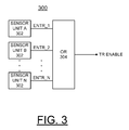
- FIG. 3 is a schematic diagram representation illustrating an example sensing system for detecting a chip tampering state in accordance with the preferred embodiment
- FIGS. 4A and 4B are respective fragmentary IC chip top and side views illustrating an example sensing device for detecting a chip tampering state in accordance with the preferred embodiment
- FIG. 5 is a schematic diagram representation illustrating an example tamper resistant control signal generator for generating a tamper resistant control signal responsive to the sensing unit detecting a chip tampering state in accordance with the preferred embodiment
- FIG. 6 is a schematic diagram representation illustrating an example functional operation inhibit circuit for inhibiting functional operation of the circuitry to be protected responsive to the tamper resistant control signal generated by the tamper resistant control signal generator of FIG. 5 in accordance with the preferred embodiment;
- FIG. 7 is a schematic diagram representation illustrating another example functional operation inhibit circuit for inhibiting functional operation of the circuitry to be protected responsive to the tamper resistant control signal generated by the tamper resistant control signal generator of FIG. 5 in accordance with the preferred embodiment.
- FIG. 8 is a flow diagram of a design process used in semiconductor design, manufacturing, and/or test.
- an enhanced method and a tamper resistant circuit for resisting tampering including reverse engineering in a semiconductor chip are provided.
- the tamper resistant circuit includes three key elements: (1) one or more sensing devices to detect that the package has been opened or removed, (2) generating at least one tamper resistance (TR) enable signal to enable TR operation and (3) disabling at least one circuit block to prevent chip from being fully operational after being tampered.
- TR tamper resistance
- FIG. 1 there are shown exemplary steps of an anti-tampering method implemented by a tamper resistant circuit for resisting reverse engineering in a semiconductor chip in accordance with the preferred embodiment.
- the TR operation should not be triggered inadvertently during normal operation.
- a sensor device or tamper sensor such as photodetector, photoresistor, or any other similar means is triggered as indicated at a block 106 .
- sensors can be built on the chip as well as on the package of a chip assembly.
- the on-chip (or off-chip) tamper sensors are photodetectors, such as a photodiode.
- photodetectors such as a photodiode.
- Other detecting schemes or mechanisms such as, an on-chip (or off-chip) solar cell, moisture sensor, micro-switch, MEMS, gas sensor, motion detector, RF detector, and the like could be used in accordance with the present invention.
- An on-chip (or off-chip) solar cell which can be used to sense module-open state, is disclosed in U.S. Pat. No. 7,098,394 to Armer et al, issued Aug. 29, 2006. These sensing devices and circuits can be integrated in the chip together with other circuits in accordance with the present invention.
- FIGS. 2A and 2B there are shown respective example package structures including wire-bond and flip-chip for use with an anti-tampering method implemented by a tamper resistant circuit for resisting reverse engineering in a semiconductor chip in accordance with the preferred embodiment.
- FIG. 2A there is shown a chip generally designated by the reference character 200 that is installed in a module via the conventional wire-bond method.
- the circuits and pads are located at the top surface of the chip are facing up. For this case, the bottom of the package and a portion of the bulk silicon below the chip must be removed, for example by precision milling or hot acid or plasma etching techniques.
- the module connections can still be used to provide power, ground and signals contacts, in order to run test patterns, and an optical sensor can sense the fact that the module has been opened, and trigger the TR signal when the chip is powered for testing. Or, the chip can be removed from the package and its backside is thinned and then remounted to the package.
- FIG. 2B shows another chip generally designated by the reference character 250 .
- Chip 250 is installed in a module by a conventional flip-chip bonding method.
- the circuits and pads are located at the top surface of the chip and are facing down.
- a backside is thinned with removed material 252 indicated by hatched lines with lines labeled h ⁇ indicating light emissions external to the IC chip 250 .
- an optical sensor can sense the module-open state and trigger the TR signal when the chip is powered for testing. Again, the thinning process can either be done with chip installed or removed from the package.
- the on-chip (or off-chip) sensing system 300 includes a plurality of sensor units 302 , A-N distributed across the chip to obtain a reliable sensing mechanism.
- Tamper sensing device 400 is a photodiode device 400 that advantageously is used to implement the plurality of sensor units 302 , A-N shown in FIG. 3 .
- the integrated photodiode 400 includes an active photodiode area 402 formed with an N diffusion 404 , and a P diffusion area 406 built into an N well 410 defined in a P-type substrate 412 within a bulk CMOS process.
- the integrated photodiode 400 is sensitive to incoming light indicated by arrows labeled h ⁇ from above or below the structure.
- CMOS-compatible sensing devices using silicon or SiGe substrates, which are well known to persons skilled in the art without requiring further description here.
- FIG. 5 there is shown an example tamper resistant control signal generator generally designated by the reference character 500 for generating a tamper resistant control signal responsive to the sensing unit detecting a chip tampering state in accordance with the preferred embodiment.
- the tamper resistant control signal generator 500 generates an output tamper-resistance enable signal ENTR_(i) responsive to detecting a chip tampering state.
- the tamper resistant control signal generator 500 includes a photodetector for sensing light or other electromagnetic energy including, for example, a photoresistor or a photodiode 400 .
- the tamper resistant control signal generator 500 includes a tamper sensing device 400 connected in series with a resistor 502 connected between a voltage supply VDD and ground.
- the tamper resistant control signal generator 500 includes at least one photodiode 400 as a light-controlled current source.
- a junction connection of the photodiode 400 and resistor 502 is applied to a first input + of an amplifier 504 having a second input ⁇ connected to an amplifier output.
- the current flow in the photodiode 400 is increased.
- the amount of light falling on the photodiode 400 directly controls the current flow.
- the current is converted to a voltage by the pull down resistor 502 thereby pulling up the voltage level to the first input + of an amplifier 504 .
- the amplifier 504 is an operational amplifier wired as a voltage follower to isolate the photodiode block from a next stage. Although not strictly necessary, the voltage follower amplifier 504 ensures the tamper detector's results are not affected by the input resistance to the next stage.
- a reset signal RST is applied to a gate of an N-channel field effect transistor 506 , which is connected between the input + of an amplifier 504 and ground.
- the reset signal RST is provided to initialize the TR signal to logic low.
- the output of the amplifier 504 is connected to a latch 508 , which is formed, by a pair of reverse connected inverters 510 , 512 .
- the latch 508 latches the data sensed by the photodiode sensor 400 , which is applied via another inverter 514 to a gate input of an NFET 516 , which is connected in series with weak pull-up device, P-channel field effect transistor (PFET) 518 .
- the weak pull-up PFET 518 and NFET 516 are connected in series between the voltage supply VDD and ground.
- the weak pull-up weak pull-up PFET 518 is used to pull the input of an inverter 520 to logic high and thus by default the output of the generator ENTR is always forced to low.
- the photodiode sensor 400 When the photodiode sensor 400 senses a tamper or module-open state, the photodiode sensor 400 switches on a strong pull down NFET 516 , which overcomes the weak pull-up PFET 518 .
- the functional operation inhibit circuit 600 includes a respective AND gate 602 , 604 , 606 each receiving an inverted TR ENABLE and a respective second input of DC ENABLE, CLOCK ENABLE, and I/O ENABLE.
- An output of the AND gate 602 provides an input to disable a DC generator 608 of the chip being protected responsive to the tamper resistant control signal TR ENABLE.
- An output of the AND gate 604 provides an input to disable a clock generator 610 of the chip being protected responsive to the tamper resistant control signal TR ENABLE.
- An output of the AND gate 606 provides an input to disable an I/O circuit 612 of the chip being protected responsive to the tamper resistant control signal TR ENABLE.
- FIG. 7 there is shown another example functional operation inhibit circuit generally designated by the reference character 700 for inhibiting functional operation of the circuitry to be protected responsive to the tamper resistant control signal generated by the tamper resistant control signal generated by the on-chip (or off-chip) sensing system 300 of FIG. 3 or tamper resistant control signal generator of FIG. 5 in accordance with the preferred embodiment.
- the functional operation inhibit circuit 700 includes a clock generator 702 and a random noise generator 704 providing inputs to a multiplexer 706 , with a select input receiving the enable control signal EN.
- the multiplexer 706 can be used to swap or replace any of various signals generated on the chip or provided from external sources with the pseudo random bit pattern to defeat reverse engineering of the chip responsive to a detected tampering state.
- the random noise generator 704 can be implemented, for example, with a design and operation of a pseudo random bit generator that is described in the U.S. Pat. No. 6,910,165 to Chen et al., entitled digital random noise generator, and assigned to the present assignee.
- FIG. 8 shows a block diagram of an example design flow 800 .
- Design flow 800 may vary depending on the type of IC being designed.
- a design flow 800 for building an application specific IC (ASIC) may differ from a design flow 800 for designing a standard component.
- Design structure 802 is preferably an input to a design process 804 and may come from an IP provider, a core developer, or other design company or may be generated by the operator of the design flow, or from other sources.
- Design structure 802 comprises circuits 300 , 400 , 500 , 600 , 700 in the form of schematics or HDL, a hardware-description language, for example, Verilog, VHDL, C, and the like.
- Design structure 802 may be contained on one or more machine readable medium.
- design structure 802 may be a text file or a graphical representation of circuits 300 , 400 , 500 , 600 , 700 .
- Design process 804 preferably synthesizes, or translates, circuits 300 , 400 , 500 , 600 , 700 into a netlist 806 , where netlist 806 is, for example, a list of wires, transistors, logic gates, control circuits, I/O, models, etc. that describes the connections to other elements and circuits in an integrated circuit design and recorded on at least one of machine readable medium. This may be an iterative process in which netlist 806 is resynthesized one or more times depending on design specifications and parameters for the circuits.
- Design process 804 may include using a variety of inputs; for example, inputs from library elements 808 which may house a set of commonly used elements, circuits, and devices, including models, layouts, and symbolic representations, for a given manufacturing technology, such as different technology nodes, 32 nm, 45 nm, 90 nm, and the like, design specifications 810 , characterization data 812 , verification data 814 , design rules 816 , and test data files 818 , which may include test patterns and other testing information. Design process 804 may further include, for example, standard circuit design processes such as timing analysis, verification, design rule checking, place and route operations, and the like.
- standard circuit design processes such as timing analysis, verification, design rule checking, place and route operations, and the like.
- Design process 804 preferably translates an embodiment of the invention as shown in FIGS. 3 , 4 A, 4 B, 5 , 6 , and 7 along with any additional integrated circuit design or data (if applicable), into a second design structure 820 .
- Design structure 820 resides on a storage medium in a data format used for the exchange of layout data of integrated circuits, for example, information stored in a GDSII (GDS2), GL1, OASIS, or any other suitable format for storing such design structures.
- GDSII GDS2
- GL1 GL1, OASIS
- Design structure 820 may comprise information such as, for example, test data files, design content files, manufacturing data, layout parameters, wires, levels of metal, vias, shapes, data for routing through the manufacturing line, and any other data required by a semiconductor manufacturer to produce an embodiment of the invention as shown in FIGS. 3 , 4 A, 4 B, 5 , 6 , and 7 .
- Design structure 820 may then proceed to a stage 822 where, for example, design structure 820 proceeds to tape-out, is released to manufacturing, is released to a mask house, is sent to another design house, is sent back to the customer, and the like.
Abstract
Description
Claims (23)
Priority Applications (1)
| Application Number | Priority Date | Filing Date | Title |
|---|---|---|---|
| US12/396,512 US8089285B2 (en) | 2009-03-03 | 2009-03-03 | Implementing tamper resistant integrated circuit chips |
Applications Claiming Priority (1)
| Application Number | Priority Date | Filing Date | Title |
|---|---|---|---|
| US12/396,512 US8089285B2 (en) | 2009-03-03 | 2009-03-03 | Implementing tamper resistant integrated circuit chips |
Publications (2)
| Publication Number | Publication Date |
|---|---|
| US20100225380A1 US20100225380A1 (en) | 2010-09-09 |
| US8089285B2 true US8089285B2 (en) | 2012-01-03 |
Family
ID=42677696
Family Applications (1)
| Application Number | Title | Priority Date | Filing Date |
|---|---|---|---|
| US12/396,512 Expired - Fee Related US8089285B2 (en) | 2009-03-03 | 2009-03-03 | Implementing tamper resistant integrated circuit chips |
Country Status (1)
| Country | Link |
|---|---|
| US (1) | US8089285B2 (en) |
Cited By (10)
| Publication number | Priority date | Publication date | Assignee | Title |
|---|---|---|---|---|
| US8730715B2 (en) * | 2012-03-26 | 2014-05-20 | Honeywell International Inc. | Tamper-resistant MRAM utilizing chemical alteration |
| US9496230B1 (en) | 2015-04-30 | 2016-11-15 | International Business Machines Corporation | Light sensitive switch for semiconductor package tamper detection |
| US10223531B2 (en) | 2016-12-30 | 2019-03-05 | Google Llc | Secure device state apparatus and method and lifecycle management |
| US10470809B1 (en) | 2018-06-19 | 2019-11-12 | Summate Technologies, Inc. | Automated screw identification system and method |
| US10671969B2 (en) | 2017-05-03 | 2020-06-02 | Summate Technologies, Inc. | Operating room situated, parts-inventory control system and supervisory arrangement for accurately tracking the use of and accounting for the ultimate disposition of an individual component part of a complete implant which is then being surgically engrafted in-vivo upon or into the body of a living subject |
| US10909343B1 (en) | 2019-07-12 | 2021-02-02 | Summate Technologies, Inc. | Automated screw identification system and method with labeled pegs |
| US11222679B2 (en) | 2019-09-17 | 2022-01-11 | Nxp Usa, Inc. | Packaged integrated circuit having a photodiode and a resistive memory |
| US11437329B2 (en) | 2020-10-14 | 2022-09-06 | Globalfoundries U.S. Inc. | Anti-tamper x-ray blocking package |
| US11815717B2 (en) | 2021-11-12 | 2023-11-14 | Globalfoundries U.S. Inc. | Photonic chip security structure |
| US11852527B2 (en) | 2020-01-07 | 2023-12-26 | Samsung Electronics Co., Ltd. | Defense circuit of semiconductor device and semiconductor device including the same |
Families Citing this family (28)
| Publication number | Priority date | Publication date | Assignee | Title |
|---|---|---|---|---|
| US8436638B2 (en) * | 2010-12-10 | 2013-05-07 | International Business Machines Corporation | Switch to perform non-destructive and secure disablement of IC functionality utilizing MEMS and method thereof |
| KR101247268B1 (en) * | 2011-08-01 | 2013-03-25 | 에스케이하이닉스 주식회사 | Semiconductor device |
| US8575560B1 (en) | 2012-06-21 | 2013-11-05 | Honeywell International Inc. | Integrated circuit cumulative dose radiation sensor |
| US8933412B2 (en) | 2012-06-21 | 2015-01-13 | Honeywell International Inc. | Integrated comparative radiation sensitive circuit |
| US9618635B2 (en) | 2012-06-21 | 2017-04-11 | Honeywell International Inc. | Integrated radiation sensitive circuit |
| TWI453923B (en) * | 2012-06-22 | 2014-09-21 | Txc Corp | Light sensing chip package structure |
| US8861728B2 (en) | 2012-10-17 | 2014-10-14 | International Business Machines Corporation | Integrated circuit tamper detection and response |
| US8816717B2 (en) | 2012-10-17 | 2014-08-26 | International Business Machines Corporation | Reactive material for integrated circuit tamper detection and response |
| WO2014153029A1 (en) * | 2013-03-14 | 2014-09-25 | New York University | System, method and computer-accessible medium for providing secure split manufacturing |
| US9154138B2 (en) | 2013-10-11 | 2015-10-06 | Palo Alto Research Center Incorporated | Stressed substrates for transient electronic systems |
| US9768128B2 (en) * | 2014-01-29 | 2017-09-19 | Infineon Technologies Ag | Chip and method for detecting an attack on a chip |
| US9246501B2 (en) | 2014-04-29 | 2016-01-26 | Honeywell International Inc. | Converter for analog inputs |
| US9780044B2 (en) | 2015-04-23 | 2017-10-03 | Palo Alto Research Center Incorporated | Transient electronic device with ion-exchanged glass treated interposer |
| US9891183B2 (en) * | 2015-07-07 | 2018-02-13 | Nxp B.V. | Breach sensor |
| US10012250B2 (en) | 2016-04-06 | 2018-07-03 | Palo Alto Research Center Incorporated | Stress-engineered frangible structures |
| US10026579B2 (en) | 2016-07-26 | 2018-07-17 | Palo Alto Research Center Incorporated | Self-limiting electrical triggering for initiating fracture of frangible glass |
| US10224297B2 (en) * | 2016-07-26 | 2019-03-05 | Palo Alto Research Center Incorporated | Sensor and heater for stimulus-initiated fracture of a substrate |
| US10586077B2 (en) | 2016-09-21 | 2020-03-10 | International Business Machines Corporation | Radio-assisted tamper protection of hardware |
| US10903173B2 (en) | 2016-10-20 | 2021-01-26 | Palo Alto Research Center Incorporated | Pre-conditioned substrate |
| US10026651B1 (en) | 2017-06-21 | 2018-07-17 | Palo Alto Research Center Incorporated | Singulation of ion-exchanged substrates |
| US10395705B2 (en) * | 2017-10-25 | 2019-08-27 | Qualcomm Incorporated | Integrated circuit copy prevention device powered by a photoelectric cell |
| US10717669B2 (en) | 2018-05-16 | 2020-07-21 | Palo Alto Research Center Incorporated | Apparatus and method for creating crack initiation sites in a self-fracturing frangible member |
| US11151290B2 (en) * | 2018-09-17 | 2021-10-19 | Analog Devices, Inc. | Tamper-resistant component networks |
| US11107645B2 (en) | 2018-11-29 | 2021-08-31 | Palo Alto Research Center Incorporated | Functionality change based on stress-engineered components |
| US10947150B2 (en) | 2018-12-03 | 2021-03-16 | Palo Alto Research Center Incorporated | Decoy security based on stress-engineered substrates |
| US10969205B2 (en) | 2019-05-03 | 2021-04-06 | Palo Alto Research Center Incorporated | Electrically-activated pressure vessels for fracturing frangible structures |
| US11904986B2 (en) | 2020-12-21 | 2024-02-20 | Xerox Corporation | Mechanical triggers and triggering methods for self-destructing frangible structures and sealed vessels |
| CN115577670B (en) * | 2022-12-07 | 2023-03-10 | 北京紫光芯能科技有限公司 | Electronic chip, detection method of electronic chip and electronic equipment |
Citations (11)
| Publication number | Priority date | Publication date | Assignee | Title |
|---|---|---|---|---|
| US6246970B1 (en) * | 1998-07-10 | 2001-06-12 | Silverbrook Research Pty Ltd | Method for making a chip tamper-resistant |
| US6496022B1 (en) | 1999-12-21 | 2002-12-17 | International Business Machines Corporation | Method and apparatus for reverse engineering integrated circuits by monitoring optical emission |
| US6910165B2 (en) | 2001-02-28 | 2005-06-21 | International Business Machines Corporation | Digital random noise generator |
| US20060081497A1 (en) * | 2002-12-18 | 2006-04-20 | Koninklijke Philips Electronics N.V. | Tamper-resistant packaging and approach |
| US7098394B2 (en) | 2001-05-15 | 2006-08-29 | Pharmaseq, Inc. | Method and apparatus for powering circuitry with on-chip solar cells within a common substrate |
| US7115912B2 (en) | 2000-06-23 | 2006-10-03 | International Business Machines Corporation | Device for defeating reverse engineering of integrated circuits by optical means |
| US20080251906A1 (en) * | 2007-04-13 | 2008-10-16 | Zilog, Inc. | Package-on-package secure module having BGA mesh cap |
| US20080251905A1 (en) * | 2007-04-13 | 2008-10-16 | Zilog, Inc. | Package-on-package secure module having anti-tamper mesh in the substrate of the upper package |
| US20100058077A1 (en) * | 2007-03-27 | 2010-03-04 | Mitsubishi Electric Corporation | Confidential information memory apparatus, erasing method of confidential information, and erasing program of confidential information |
| US7685438B2 (en) * | 2003-01-14 | 2010-03-23 | Nxp B.V. | Tamper-resistant packaging and approach using magnetically-set data |
| US7945792B2 (en) * | 2007-10-17 | 2011-05-17 | Spansion Llc | Tamper reactive memory device to secure data from tamper attacks |
-
2009
- 2009-03-03 US US12/396,512 patent/US8089285B2/en not_active Expired - Fee Related
Patent Citations (11)
| Publication number | Priority date | Publication date | Assignee | Title |
|---|---|---|---|---|
| US6246970B1 (en) * | 1998-07-10 | 2001-06-12 | Silverbrook Research Pty Ltd | Method for making a chip tamper-resistant |
| US6496022B1 (en) | 1999-12-21 | 2002-12-17 | International Business Machines Corporation | Method and apparatus for reverse engineering integrated circuits by monitoring optical emission |
| US7115912B2 (en) | 2000-06-23 | 2006-10-03 | International Business Machines Corporation | Device for defeating reverse engineering of integrated circuits by optical means |
| US6910165B2 (en) | 2001-02-28 | 2005-06-21 | International Business Machines Corporation | Digital random noise generator |
| US7098394B2 (en) | 2001-05-15 | 2006-08-29 | Pharmaseq, Inc. | Method and apparatus for powering circuitry with on-chip solar cells within a common substrate |
| US20060081497A1 (en) * | 2002-12-18 | 2006-04-20 | Koninklijke Philips Electronics N.V. | Tamper-resistant packaging and approach |
| US7685438B2 (en) * | 2003-01-14 | 2010-03-23 | Nxp B.V. | Tamper-resistant packaging and approach using magnetically-set data |
| US20100058077A1 (en) * | 2007-03-27 | 2010-03-04 | Mitsubishi Electric Corporation | Confidential information memory apparatus, erasing method of confidential information, and erasing program of confidential information |
| US20080251906A1 (en) * | 2007-04-13 | 2008-10-16 | Zilog, Inc. | Package-on-package secure module having BGA mesh cap |
| US20080251905A1 (en) * | 2007-04-13 | 2008-10-16 | Zilog, Inc. | Package-on-package secure module having anti-tamper mesh in the substrate of the upper package |
| US7945792B2 (en) * | 2007-10-17 | 2011-05-17 | Spansion Llc | Tamper reactive memory device to secure data from tamper attacks |
Cited By (11)
| Publication number | Priority date | Publication date | Assignee | Title |
|---|---|---|---|---|
| US8730715B2 (en) * | 2012-03-26 | 2014-05-20 | Honeywell International Inc. | Tamper-resistant MRAM utilizing chemical alteration |
| US9496230B1 (en) | 2015-04-30 | 2016-11-15 | International Business Machines Corporation | Light sensitive switch for semiconductor package tamper detection |
| US10223531B2 (en) | 2016-12-30 | 2019-03-05 | Google Llc | Secure device state apparatus and method and lifecycle management |
| US10872154B2 (en) | 2016-12-30 | 2020-12-22 | Google Llc | Secure device state apparatus and method and lifecycle management |
| US10671969B2 (en) | 2017-05-03 | 2020-06-02 | Summate Technologies, Inc. | Operating room situated, parts-inventory control system and supervisory arrangement for accurately tracking the use of and accounting for the ultimate disposition of an individual component part of a complete implant which is then being surgically engrafted in-vivo upon or into the body of a living subject |
| US10470809B1 (en) | 2018-06-19 | 2019-11-12 | Summate Technologies, Inc. | Automated screw identification system and method |
| US10909343B1 (en) | 2019-07-12 | 2021-02-02 | Summate Technologies, Inc. | Automated screw identification system and method with labeled pegs |
| US11222679B2 (en) | 2019-09-17 | 2022-01-11 | Nxp Usa, Inc. | Packaged integrated circuit having a photodiode and a resistive memory |
| US11852527B2 (en) | 2020-01-07 | 2023-12-26 | Samsung Electronics Co., Ltd. | Defense circuit of semiconductor device and semiconductor device including the same |
| US11437329B2 (en) | 2020-10-14 | 2022-09-06 | Globalfoundries U.S. Inc. | Anti-tamper x-ray blocking package |
| US11815717B2 (en) | 2021-11-12 | 2023-11-14 | Globalfoundries U.S. Inc. | Photonic chip security structure |
Also Published As
| Publication number | Publication date |
|---|---|
| US20100225380A1 (en) | 2010-09-09 |
Similar Documents
| Publication | Publication Date | Title |
|---|---|---|
| US8089285B2 (en) | Implementing tamper resistant integrated circuit chips | |
| US7791087B2 (en) | Device for defeating reverse engineering of integrated circuits by optical means | |
| Guin et al. | Low-cost on-chip structures for combating die and IC recycling | |
| US7969763B2 (en) | Detector circuit for detecting an external manipulation of an electrical circuit, circuit arrangement comprising a plurality of detector circuits, memory device and method for operating a detector circuit | |
| JP5387144B2 (en) | Malfunction occurrence attack detection circuit and integrated circuit | |
| US7474112B2 (en) | Method and apparatus for non-invasively testing integrated circuits | |
| US5861652A (en) | Method and apparatus for protecting functions imbedded within an integrated circuit from reverse engineering | |
| KR19980071048A (en) | Wafers, test systems, methods of performing the same, data processors, and methods of inspecting the same | |
| Steininger | Testing and built-in self-test–A survey | |
| Dutertre et al. | Improving the ability of Bulk Built-In Current Sensors to detect Single Event Effects by using triple-well CMOS | |
| JP2008198700A (en) | Semiconductor integrated circuit device | |
| US20130280828A1 (en) | Minimum-spacing circuit design and layout for pica | |
| Song et al. | Counterfeit IC detection using light emission | |
| Selmke et al. | Locked out by latch-up? An empirical study on laser fault injection into Arm Cortex-M processors | |
| Alnuayri et al. | Differential aging sensor to detect recycled ICs using sub-threshold leakage current | |
| Li et al. | Security evaluation at design time against optical fault injection attacks | |
| Goh et al. | A detailed analysis scheme to interpret multiple photon emissions micrograph for improved diagnostic resolution on open defects | |
| Burmer et al. | Failure analyses for debug and ramp-up of modern IC’s | |
| EP2541599A1 (en) | Security semiconductor product | |
| JPH06281700A (en) | Method and device for analyzing fault of semiconductor device | |
| Nagata | Exploring fault injection attack resilience of secure ic chips | |
| US9343377B1 (en) | Test then destroy technique for security-focused semiconductor integrated circuits | |
| JP2009231375A (en) | Semiconductor device including connection detection circuit | |
| Matsumoto et al. | Studying LSI Tamper Resistance with Respect to Techniques Developed for Failure Analysis | |
| Mak et al. | Design for debug and diagnosis |
Legal Events
| Date | Code | Title | Description |
|---|---|---|---|
| AS | Assignment |
Owner name: INTERNATIONAL BUSINESS MACHINES CORPORATION, NEW Y Free format text: ASSIGNMENT OF ASSIGNORS INTEREST;ASSIGNORS:HSU, LOUIS L.;KRUGER, DAVD W.;MASON, JAMES S.;AND OTHERS;SIGNING DATES FROM 20090213 TO 20090219;REEL/FRAME:022334/0779 |
|
| AS | Assignment |
Owner name: INTERNATIONAL BUSINESS MACHINES CORPORATION, NEW Y Free format text: CORRECTIVE ASSIGNMENT TO CORRECT THE ASSIGNOR KRUGER, DAVD W. SHOULD BE KRUGER, DAVID W. PREVIOUSLY RECORDED ON REEL 922334 FRAME 0779. ASSIGNOR(S) HEREBY CONFIRMS THE KRUGER, DAVD W. SHOULD BE KRUGER, DAVID W.;ASSIGNORS:HSU, LOUIS L.;KRUGER, DAVID W.;MASON, JAMES E.;AND OTHERS;SIGNING DATES FROM 20090213 TO 20090219;REEL/FRAME:022341/0944 |
|
| ZAAA | Notice of allowance and fees due |
Free format text: ORIGINAL CODE: NOA |
|
| ZAAB | Notice of allowance mailed |
Free format text: ORIGINAL CODE: MN/=. |
|
| STCF | Information on status: patent grant |
Free format text: PATENTED CASE |
|
| FPAY | Fee payment |
Year of fee payment: 4 |
|
| FEPP | Fee payment procedure |
Free format text: MAINTENANCE FEE REMINDER MAILED (ORIGINAL EVENT CODE: REM.); ENTITY STATUS OF PATENT OWNER: LARGE ENTITY |
|
| AS | Assignment |
Owner name: DAEDALUS GROUP LLC, NEW YORK Free format text: ASSIGNMENT OF ASSIGNORS INTEREST;ASSIGNOR:INTERNATIONAL BUSINESS MACHINES CORPORATION;REEL/FRAME:051032/0784 Effective date: 20190930 |
|
| FEPP | Fee payment procedure |
Free format text: 7.5 YR SURCHARGE - LATE PMT W/IN 6 MO, LARGE ENTITY (ORIGINAL EVENT CODE: M1555); ENTITY STATUS OF PATENT OWNER: LARGE ENTITY |
|
| MAFP | Maintenance fee payment |
Free format text: PAYMENT OF MAINTENANCE FEE, 8TH YEAR, LARGE ENTITY (ORIGINAL EVENT CODE: M1552); ENTITY STATUS OF PATENT OWNER: LARGE ENTITY Year of fee payment: 8 |
|
| AS | Assignment |
Owner name: DAEDALUS GROUP, LLC, NEW YORK Free format text: ASSIGNMENT OF ASSIGNORS INTEREST;ASSIGNOR:INTERNATIONAL BUSINESS MACHINES CORPORATION;REEL/FRAME:051710/0445 Effective date: 20191230 |
|
| AS | Assignment |
Owner name: DAEDALUS BLUE LLC, NEW YORK Free format text: ASSIGNMENT OF ASSIGNORS INTEREST;ASSIGNOR:DAEDALUS GROUP, LLC;REEL/FRAME:051737/0191 Effective date: 20200128 |
|
| AS | Assignment |
Owner name: TERRACE LICENSING LLC, TEXAS Free format text: ASSIGNMENT OF ASSIGNORS INTEREST;ASSIGNOR:DAEDALUS BLUE LLC;REEL/FRAME:058895/0322 Effective date: 20211129 |
|
| AS | Assignment |
Owner name: TERRACE LICENSING LLC, TEXAS Free format text: ASSIGNMENT OF ASSIGNORS INTEREST;ASSIGNOR:DAEDALUS BLUE LLC;REEL/FRAME:058902/0482 Effective date: 20211129 |
|
| FEPP | Fee payment procedure |
Free format text: MAINTENANCE FEE REMINDER MAILED (ORIGINAL EVENT CODE: REM.); ENTITY STATUS OF PATENT OWNER: LARGE ENTITY |
|
| LAPS | Lapse for failure to pay maintenance fees |
Free format text: PATENT EXPIRED FOR FAILURE TO PAY MAINTENANCE FEES (ORIGINAL EVENT CODE: EXP.); ENTITY STATUS OF PATENT OWNER: LARGE ENTITY |
|
| STCH | Information on status: patent discontinuation |
Free format text: PATENT EXPIRED DUE TO NONPAYMENT OF MAINTENANCE FEES UNDER 37 CFR 1.362 |
|
| FP | Lapsed due to failure to pay maintenance fee |
Effective date: 20240103 |