US8097080B2 - Method of cutting single crystals - Google Patents
Method of cutting single crystals Download PDFInfo
- Publication number
- US8097080B2 US8097080B2 US12/271,245 US27124508A US8097080B2 US 8097080 B2 US8097080 B2 US 8097080B2 US 27124508 A US27124508 A US 27124508A US 8097080 B2 US8097080 B2 US 8097080B2
- Authority
- US
- United States
- Prior art keywords
- crack
- stress
- cleavage
- energy
- propagation
- Prior art date
- Legal status (The legal status is an assumption and is not a legal conclusion. Google has not performed a legal analysis and makes no representation as to the accuracy of the status listed.)
- Active, expires
Links
Images


Classifications
-
- H—ELECTRICITY
- H01—ELECTRIC ELEMENTS
- H01L—SEMICONDUCTOR DEVICES NOT COVERED BY CLASS H10
- H01L21/00—Processes or apparatus adapted for the manufacture or treatment of semiconductor or solid state devices or of parts thereof
- H01L21/70—Manufacture or treatment of devices consisting of a plurality of solid state components formed in or on a common substrate or of parts thereof; Manufacture of integrated circuit devices or of parts thereof
- H01L21/77—Manufacture or treatment of devices consisting of a plurality of solid state components or integrated circuits formed in, or on, a common substrate
- H01L21/78—Manufacture or treatment of devices consisting of a plurality of solid state components or integrated circuits formed in, or on, a common substrate with subsequent division of the substrate into plural individual devices
-
- B—PERFORMING OPERATIONS; TRANSPORTING
- B28—WORKING CEMENT, CLAY, OR STONE
- B28D—WORKING STONE OR STONE-LIKE MATERIALS
- B28D5/00—Fine working of gems, jewels, crystals, e.g. of semiconductor material; apparatus or devices therefor
-
- B—PERFORMING OPERATIONS; TRANSPORTING
- B28—WORKING CEMENT, CLAY, OR STONE
- B28D—WORKING STONE OR STONE-LIKE MATERIALS
- B28D5/00—Fine working of gems, jewels, crystals, e.g. of semiconductor material; apparatus or devices therefor
- B28D5/0058—Accessories specially adapted for use with machines for fine working of gems, jewels, crystals, e.g. of semiconductor material
- B28D5/0064—Devices for the automatic drive or the program control of the machines
-
- Y—GENERAL TAGGING OF NEW TECHNOLOGICAL DEVELOPMENTS; GENERAL TAGGING OF CROSS-SECTIONAL TECHNOLOGIES SPANNING OVER SEVERAL SECTIONS OF THE IPC; TECHNICAL SUBJECTS COVERED BY FORMER USPC CROSS-REFERENCE ART COLLECTIONS [XRACs] AND DIGESTS
- Y10—TECHNICAL SUBJECTS COVERED BY FORMER USPC
- Y10S—TECHNICAL SUBJECTS COVERED BY FORMER USPC CROSS-REFERENCE ART COLLECTIONS [XRACs] AND DIGESTS
- Y10S117/00—Single-crystal, oriented-crystal, and epitaxy growth processes; non-coating apparatus therefor
- Y10S117/915—Separating from substrate
-
- Y—GENERAL TAGGING OF NEW TECHNOLOGICAL DEVELOPMENTS; GENERAL TAGGING OF CROSS-SECTIONAL TECHNOLOGIES SPANNING OVER SEVERAL SECTIONS OF THE IPC; TECHNICAL SUBJECTS COVERED BY FORMER USPC CROSS-REFERENCE ART COLLECTIONS [XRACs] AND DIGESTS
- Y10—TECHNICAL SUBJECTS COVERED BY FORMER USPC
- Y10T—TECHNICAL SUBJECTS COVERED BY FORMER US CLASSIFICATION
- Y10T225/00—Severing by tearing or breaking
- Y10T225/10—Methods
- Y10T225/12—With preliminary weakening
-
- Y—GENERAL TAGGING OF NEW TECHNOLOGICAL DEVELOPMENTS; GENERAL TAGGING OF CROSS-SECTIONAL TECHNOLOGIES SPANNING OVER SEVERAL SECTIONS OF THE IPC; TECHNICAL SUBJECTS COVERED BY FORMER USPC CROSS-REFERENCE ART COLLECTIONS [XRACs] AND DIGESTS
- Y10—TECHNICAL SUBJECTS COVERED BY FORMER USPC
- Y10T—TECHNICAL SUBJECTS COVERED BY FORMER US CLASSIFICATION
- Y10T428/00—Stock material or miscellaneous articles
- Y10T428/24—Structurally defined web or sheet [e.g., overall dimension, etc.]
- Y10T428/24802—Discontinuous or differential coating, impregnation or bond [e.g., artwork, printing, retouched photograph, etc.]
-
- Y—GENERAL TAGGING OF NEW TECHNOLOGICAL DEVELOPMENTS; GENERAL TAGGING OF CROSS-SECTIONAL TECHNOLOGIES SPANNING OVER SEVERAL SECTIONS OF THE IPC; TECHNICAL SUBJECTS COVERED BY FORMER USPC CROSS-REFERENCE ART COLLECTIONS [XRACs] AND DIGESTS
- Y10—TECHNICAL SUBJECTS COVERED BY FORMER USPC
- Y10T—TECHNICAL SUBJECTS COVERED BY FORMER US CLASSIFICATION
- Y10T428/00—Stock material or miscellaneous articles
- Y10T428/31504—Composite [nonstructural laminate]
- Y10T428/31678—Of metal
Landscapes
- Engineering & Computer Science (AREA)
- Mechanical Engineering (AREA)
- Physics & Mathematics (AREA)
- Condensed Matter Physics & Semiconductors (AREA)
- General Physics & Mathematics (AREA)
- Manufacturing & Machinery (AREA)
- Computer Hardware Design (AREA)
- Microelectronics & Electronic Packaging (AREA)
- Power Engineering (AREA)
- Crystals, And After-Treatments Of Crystals (AREA)
- Processing Of Stones Or Stones Resemblance Materials (AREA)
- Dicing (AREA)
Abstract
Description
K>KC, (1.1)
wherein KC is the critical stress-intensity factor specific for the material, the crack length increases until the condition
K≦KC (1.2)
is fulfilled. K>KC is the propagation condition of the separation process, which has to be maintained continually or in intervals, until the complete separation is achieved.
wherein U denotes the total energy of the system, and C denotes the surface area generated by means of crack propagation.
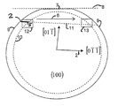
- α possible deflection angle upon crack propagation from the cleavage plane
- α1, α2 range of angles, in which the necessary condition for a crack propagation (1.1) is satisfied
- G(α) mechanical-energy-release rate in dependence of a deflection of the crack from the cleavage plane about angle α.
- γe(0) effective surface energy of cleavage surface
- γe effective surface energy depending on direction
- βe effective step energy (material specific)
- h step height (material specific).
βe =−nk B T ln η(1+2η),
η=exp(−ε/k B T).
ε≈ΔH sub /Z,
wherein ΔHsub(T) is obtained from a calculation of the thermo-dynamic equilibrium Xs
ΔH sub(300 K)=451.4 kJ/mol,
Z=4
→ε≈1.17 eV;
-
- and for T=300 K: η≈45.25.
βe≈3.31·10−10 J/m, and
βe /h≈0.83 J/m2.
In
In
are fulfilled for both functions G−(α) and G+(α). Thereby it is ensured that for each intermediate state G(α) the conditions according to certain embodiments of the invention are satisfied as well, and the crack remains within the cleavage plane during the complete dividing process.
must be valid for condition (2.1), or G(α)≧2γe(α) must be valid for condition (2.2), respectively. The determined angular range is then compared with a predetermined mean alignment- or adjustment-error of an orientation of the crystallographic (2′) relative to the separation device. The control of the stress fields (3′, 4′) and/or the adaption of the pre-adjustment of the crystal is then carried out in dependence of the result of the comparison.
Claims (14)
Priority Applications (2)
| Application Number | Priority Date | Filing Date | Title |
|---|---|---|---|
| US12/271,245 US8097080B2 (en) | 2007-11-15 | 2008-11-14 | Method of cutting single crystals |
| US13/226,519 US8723288B2 (en) | 2007-11-15 | 2011-09-07 | Method of cutting single crystals |
Applications Claiming Priority (5)
| Application Number | Priority Date | Filing Date | Title |
|---|---|---|---|
| US99639607P | 2007-11-15 | 2007-11-15 | |
| DE102007056115.8 | 2007-11-15 | ||
| DE200710056115 DE102007056115A1 (en) | 2007-11-15 | 2007-11-15 | Process for separating single crystals |
| DE102007056115 | 2007-11-15 | ||
| US12/271,245 US8097080B2 (en) | 2007-11-15 | 2008-11-14 | Method of cutting single crystals |
Related Child Applications (1)
| Application Number | Title | Priority Date | Filing Date |
|---|---|---|---|
| US13/226,519 Division US8723288B2 (en) | 2007-11-15 | 2011-09-07 | Method of cutting single crystals |
Publications (2)
| Publication Number | Publication Date |
|---|---|
| US20090283761A1 US20090283761A1 (en) | 2009-11-19 |
| US8097080B2 true US8097080B2 (en) | 2012-01-17 |
Family
ID=40560840
Family Applications (2)
| Application Number | Title | Priority Date | Filing Date |
|---|---|---|---|
| US12/271,245 Active 2030-07-14 US8097080B2 (en) | 2007-11-15 | 2008-11-14 | Method of cutting single crystals |
| US13/226,519 Active US8723288B2 (en) | 2007-11-15 | 2011-09-07 | Method of cutting single crystals |
Family Applications After (1)
| Application Number | Title | Priority Date | Filing Date |
|---|---|---|---|
| US13/226,519 Active US8723288B2 (en) | 2007-11-15 | 2011-09-07 | Method of cutting single crystals |
Country Status (7)
| Country | Link |
|---|---|
| US (2) | US8097080B2 (en) |
| EP (2) | EP2377662A1 (en) |
| JP (2) | JP5697984B2 (en) |
| CN (1) | CN101861237B (en) |
| AT (1) | ATE543622T1 (en) |
| DE (1) | DE102007056115A1 (en) |
| WO (1) | WO2009062744A1 (en) |
Cited By (1)
| Publication number | Priority date | Publication date | Assignee | Title |
|---|---|---|---|---|
| US20100310775A1 (en) * | 2009-06-09 | 2010-12-09 | International Business Machines Corporation | Spalling for a Semiconductor Substrate |
Families Citing this family (8)
| Publication number | Priority date | Publication date | Assignee | Title |
|---|---|---|---|---|
| KR100945506B1 (en) * | 2007-06-26 | 2010-03-09 | 주식회사 하이닉스반도체 | Semiconductor substrate and method of manufacturing semiconductor package using the semiconductor substrate |
| US20160008926A1 (en) * | 2014-07-14 | 2016-01-14 | Rubicon Technology, Inc. | Method of cold-cleaving sapphire material at cryogenic temperatures |
| CN107922259B (en) * | 2015-09-04 | 2021-05-07 | Agc株式会社 | Method for producing glass plate, method for producing glass article, and apparatus for producing glass article |
| FR3055063B1 (en) * | 2016-08-11 | 2018-08-31 | Soitec | METHOD OF TRANSFERRING A USEFUL LAYER |
| JP6795811B2 (en) * | 2017-02-16 | 2020-12-02 | 国立大学法人埼玉大学 | Peeling substrate manufacturing method |
| EP3795855A1 (en) * | 2019-09-20 | 2021-03-24 | Patek Philippe SA Genève | Method for producing a timepiece spring from monocrystalline material and timepiece spring obtained by said method |
| CN111640687B (en) * | 2020-06-08 | 2023-03-14 | 郑州磨料磨具磨削研究所有限公司 | Method for determining optimal scribing direction of single crystal wafer |
| CN114393723B (en) * | 2022-01-20 | 2023-06-13 | 中环领先半导体材料有限公司 | Method for realizing integration of positioning slotting re-inspection and self-inspection of barreling equipment |
Citations (11)
| Publication number | Priority date | Publication date | Assignee | Title |
|---|---|---|---|---|
| DE2813302B1 (en) | 1978-03-28 | 1979-01-11 | Fraunhofer Ges Forschung | Method and device for straight-line cutting of flat glass with the aid of thermally induced stresses |
| US4244348A (en) * | 1979-09-10 | 1981-01-13 | Atlantic Richfield Company | Process for cleaving crystalline materials |
| US5154333A (en) | 1991-10-30 | 1992-10-13 | International Business Machines Corporation | Jaw cleaving device |
| WO1993020015A1 (en) | 1992-04-02 | 1993-10-14 | Fonon Technology Limited | Splitting of non-metallic materials |
| US5279077A (en) | 1992-03-12 | 1994-01-18 | Mitsubishi Denki Kabushiki Kaisha | Method for producing semiconductor wafer |
| US5393707A (en) * | 1992-07-31 | 1995-02-28 | Northern Telecom Limited | Semiconductor - slice cleaving |
| EP0961328A2 (en) | 1998-05-28 | 1999-12-01 | Sumitomo Electric Industries, Ltd. | Gallium nitride-type semiconductor device |
| US6252197B1 (en) | 1998-12-01 | 2001-06-26 | Accudyne Display And Semiconductor Systems, Inc. | Method and apparatus for separating non-metallic substrates utilizing a supplemental mechanical force applicator |
| JP2006024839A (en) | 2004-07-09 | 2006-01-26 | Sumitomo Metal Mining Co Ltd | Method for cleaving semiconductor wafer and associated jig |
| EP1768181A1 (en) | 2005-09-07 | 2007-03-28 | Sumitomo Electric Industries, Ltd. | Nitride semiconductor substrate, and method for working nitride semiconductor substrate |
| US20080179547A1 (en) * | 2006-09-08 | 2008-07-31 | Silicon Genesis Corporation | Method and structure for fabricating solar cells using a thick layer transfer process |
Family Cites Families (14)
| Publication number | Priority date | Publication date | Assignee | Title |
|---|---|---|---|---|
| US5198069A (en) * | 1989-12-04 | 1993-03-30 | Loral Infrared & Imaging Systems, Inc. | Method for fabricating buttable epitaxial infrared detector arrays by dimensionally controlled cleaving of single crystal substrates |
| JPH0555143A (en) * | 1991-08-27 | 1993-03-05 | Mitsubishi Electric Corp | Method for growing crystal on circular wafer |
| CN1113269A (en) * | 1995-01-29 | 1995-12-13 | 陈秋生 | Method for production of single alundum |
| JPH091370A (en) * | 1995-06-20 | 1997-01-07 | Souei Tsusho Kk | Splitting method and its device |
| JP3580631B2 (en) * | 1996-02-29 | 2004-10-27 | 京セラ株式会社 | Single crystal sapphire substrate, method of dividing single crystal sapphire, and single crystal sapphire body |
| JPH09256472A (en) | 1996-03-19 | 1997-09-30 | Sumitomo Forestry Co Ltd | Housing unit and assembly method therefor |
| CN1064723C (en) * | 1997-12-11 | 2001-04-18 | 西北有色金属研究院 | Method for preparing neodymium barium copper oxygen superconductive monocrystal |
| CN1241803A (en) * | 1998-05-15 | 2000-01-19 | 佳能株式会社 | Process for manufacturing semiconductor substrate as well as semiconductor thin film and multilayer structure |
| FR2828428B1 (en) * | 2001-08-07 | 2003-10-17 | Soitec Silicon On Insulator | DEVICE FOR PICKING UP SUBSTRATES AND ASSOCIATED METHOD |
| JP4566478B2 (en) * | 2001-08-09 | 2010-10-20 | シルトロニック・ジャパン株式会社 | Silicon semiconductor substrate and manufacturing method thereof |
| JP3982324B2 (en) | 2002-05-15 | 2007-09-26 | 日本電気株式会社 | Vector operation processing device, vector operation method, and vector operation program |
| JP2004063860A (en) * | 2002-07-30 | 2004-02-26 | Matsushita Electric Ind Co Ltd | Semiconductor device and its manufacturing method |
| US7687372B2 (en) * | 2005-04-08 | 2010-03-30 | Versatilis Llc | System and method for manufacturing thick and thin film devices using a donee layer cleaved from a crystalline donor |
| JP2008183599A (en) * | 2007-01-31 | 2008-08-14 | Japan Steel Works Ltd:The | Method for working workpiece made of highly brittle and non-metallic material, and device therefor |
-
2007
- 2007-11-15 DE DE200710056115 patent/DE102007056115A1/en not_active Ceased
-
2008
- 2008-11-14 US US12/271,245 patent/US8097080B2/en active Active
- 2008-11-14 WO PCT/EP2008/009676 patent/WO2009062744A1/en active Application Filing
- 2008-11-14 JP JP2010533506A patent/JP5697984B2/en active Active
- 2008-11-14 EP EP20110174244 patent/EP2377662A1/en not_active Ceased
- 2008-11-14 EP EP08850859A patent/EP2106331B1/en active Active
- 2008-11-14 CN CN200880116181.7A patent/CN101861237B/en active Active
- 2008-11-14 AT AT08850859T patent/ATE543622T1/en active
-
2011
- 2011-09-07 US US13/226,519 patent/US8723288B2/en active Active
-
2014
- 2014-06-04 JP JP2014115493A patent/JP2014218428A/en active Pending
Patent Citations (12)
| Publication number | Priority date | Publication date | Assignee | Title |
|---|---|---|---|---|
| DE2813302B1 (en) | 1978-03-28 | 1979-01-11 | Fraunhofer Ges Forschung | Method and device for straight-line cutting of flat glass with the aid of thermally induced stresses |
| US4244348A (en) * | 1979-09-10 | 1981-01-13 | Atlantic Richfield Company | Process for cleaving crystalline materials |
| US5154333A (en) | 1991-10-30 | 1992-10-13 | International Business Machines Corporation | Jaw cleaving device |
| US5279077A (en) | 1992-03-12 | 1994-01-18 | Mitsubishi Denki Kabushiki Kaisha | Method for producing semiconductor wafer |
| US5439723A (en) | 1992-03-12 | 1995-08-08 | Mitsubishi Denki Kabushiki Kaisha | Substrate for producing semiconductor wafer |
| WO1993020015A1 (en) | 1992-04-02 | 1993-10-14 | Fonon Technology Limited | Splitting of non-metallic materials |
| US5393707A (en) * | 1992-07-31 | 1995-02-28 | Northern Telecom Limited | Semiconductor - slice cleaving |
| EP0961328A2 (en) | 1998-05-28 | 1999-12-01 | Sumitomo Electric Industries, Ltd. | Gallium nitride-type semiconductor device |
| US6252197B1 (en) | 1998-12-01 | 2001-06-26 | Accudyne Display And Semiconductor Systems, Inc. | Method and apparatus for separating non-metallic substrates utilizing a supplemental mechanical force applicator |
| JP2006024839A (en) | 2004-07-09 | 2006-01-26 | Sumitomo Metal Mining Co Ltd | Method for cleaving semiconductor wafer and associated jig |
| EP1768181A1 (en) | 2005-09-07 | 2007-03-28 | Sumitomo Electric Industries, Ltd. | Nitride semiconductor substrate, and method for working nitride semiconductor substrate |
| US20080179547A1 (en) * | 2006-09-08 | 2008-07-31 | Silicon Genesis Corporation | Method and structure for fabricating solar cells using a thick layer transfer process |
Non-Patent Citations (7)
| Title |
|---|
| Bechstedt, F., "Principles of Surface Physics", Springer, 2003, pp. 16-18. |
| Belsinger et al., "A Fracture Criterion for Gallium Arsenide Wafers", Engineering Fracture Mechanics, 48(2), 1994, pp. 199-203, 205. |
| Faber et al., "Crack Deflection Processes-I. Theory", Acta Metallurgica, 31(4), 1983, pp. 565-576. |
| Hammer et al., "Material related fundamentals of cutting techniques for GaAs wafer manufacturing", Z. Metallkd., 96(7), 2005, pp. 787-793. |
| Paterson et al., "On the numerical modelling of laser shearing of glass sheets used to optimize production methods", Proc. Instn. Mech. Engrs., 218(1), Part C: J. Mechanical Engineering Science, 2004, pp. 1-11. |
| Qian et al., "First-principles calculations of atomic and electronic structure of the GaAs(110) surface", Physical Review B, vol. 37, No. 3, Jan. 15, 1988, pp. 1303-1307. |
| R. K. Sink et al., "Cleaved GaN facets by water fusion of GaN to InP", American Institute of Physics, Applied Physics Letter, vol. 68, No. 15, Apr. 8, 1996, pp. 2147-2149. |
Cited By (1)
| Publication number | Priority date | Publication date | Assignee | Title |
|---|---|---|---|---|
| US20100310775A1 (en) * | 2009-06-09 | 2010-12-09 | International Business Machines Corporation | Spalling for a Semiconductor Substrate |
Also Published As
| Publication number | Publication date |
|---|---|
| CN101861237B (en) | 2015-06-24 |
| JP2014218428A (en) | 2014-11-20 |
| EP2106331B1 (en) | 2012-02-01 |
| JP5697984B2 (en) | 2015-04-08 |
| US8723288B2 (en) | 2014-05-13 |
| EP2377662A1 (en) | 2011-10-19 |
| CN101861237A (en) | 2010-10-13 |
| EP2106331A1 (en) | 2009-10-07 |
| WO2009062744A1 (en) | 2009-05-22 |
| US20110318221A1 (en) | 2011-12-29 |
| DE102007056115A1 (en) | 2009-05-20 |
| US20090283761A1 (en) | 2009-11-19 |
| JP2011503888A (en) | 2011-01-27 |
| ATE543622T1 (en) | 2012-02-15 |
Similar Documents
| Publication | Publication Date | Title |
|---|---|---|
| US8097080B2 (en) | Method of cutting single crystals | |
| US11444221B2 (en) | Layer transfer of films utilizing controlled shear region | |
| CN101443488B (en) | Process for producing a III-N bulk crystal and a free-standing III-N substrate, and III-N bulk crystal and free-standing III-N substrate | |
| US11183358B2 (en) | Energy filter element for ion implantation systems for the use in the production of wafers | |
| KR20100027046A (en) | Layer transfer of films utilizing controlled propagation | |
| Tripathy et al. | Optical properties of GaN layers grown on C-, A-, R-, and M-plane sapphire substrates by gas source molecular beam epitaxy | |
| CN104781938B (en) | Multi-layer substrate structure and the method and system for manufacturing it | |
| Kamiński et al. | Effect of oxidation temperature on the inhomogeneity of chemical composition and density in nanometric SiO 2 films grown on 4H-SiC | |
| KR20170056748A (en) | Method of excimer laser annealing | |
| US7400376B2 (en) | Apparatus and method for forming alignment layer | |
| Kosiel et al. | Multi-step interrupted-growth MBE technology for GaAs/AlGaAs (∼ 9.4 μm) room temperature operating quantum-cascade lasers | |
| Turos et al. | Stopping power and energy straggling of channeled He-ions in GaN | |
| Feng et al. | Depth dependent elastic strain in ZnO epilayer: combined Rutherford backscattering/channeling and X-ray diffraction | |
| Ahmed | Growth and Characterization of Nitride Semiconductors on Chemical Vapor Deposited Diamond | |
| Urban | Position-controlled selective area growth of Ga-polar GaN nanocolumns by molecular beam epitaxy: A versatile approach towards semipolar GaN and the characterization of single nanocolumns | |
| CN107785461B (en) | A kind of laser assisted direct band gap Ge and preparation method thereof on crystallization Ge/Si void substrate again | |
| JP2004284101A (en) | Processing method using beam and apparatus therefor | |
| Morris et al. | Imperfect low-angle boundaries and fracture in hydrothermally grown berlinite crystals | |
| Hossain | A novel process for germanium silicide thin film synthesis | |
| Dalmau | Aluminum Nitride bulk crystal growth in a resistively heated reactor | |
| JPS60102786A (en) | Manufacture of bar single crystal material and manufacturing device thereof | |
| Friel | Molecular beam epitaxy growth of aluminum gallium nitride/gallium nitride quantum wells and investigation of excitonic and intersubband transitions | |
| JP2002331518A (en) | Method for cutting single crystal ingot | |
| Zauner | Homo-and hetero-epitaxial growth of gallium nitride by metalorganic chemical vapour deposition | |
| Herman et al. | Solid Phase Epitaxy |
Legal Events
| Date | Code | Title | Description |
|---|---|---|---|
| AS | Assignment |
Owner name: FREIBERGER COMPOUND MATERIALS GMBH, GERMANY Free format text: ASSIGNMENT OF ASSIGNORS INTEREST;ASSIGNORS:HAMMER, RALF;JURISCH, MANFRED;REEL/FRAME:022198/0771 Effective date: 20090113 |
|
| STCF | Information on status: patent grant |
Free format text: PATENTED CASE |
|
| FPAY | Fee payment |
Year of fee payment: 4 |
|
| MAFP | Maintenance fee payment |
Free format text: PAYMENT OF MAINTENANCE FEE, 8TH YEAR, LARGE ENTITY (ORIGINAL EVENT CODE: M1552); ENTITY STATUS OF PATENT OWNER: LARGE ENTITY Year of fee payment: 8 |
|
| MAFP | Maintenance fee payment |
Free format text: PAYMENT OF MAINTENANCE FEE, 12TH YEAR, LARGE ENTITY (ORIGINAL EVENT CODE: M1553); ENTITY STATUS OF PATENT OWNER: LARGE ENTITY Year of fee payment: 12 |