US8099561B2 - Shared memory system for a tightly-coupled multiprocessor - Google Patents
Shared memory system for a tightly-coupled multiprocessor Download PDFInfo
- Publication number
- US8099561B2 US8099561B2 US12/267,591 US26759108A US8099561B2 US 8099561 B2 US8099561 B2 US 8099561B2 US 26759108 A US26759108 A US 26759108A US 8099561 B2 US8099561 B2 US 8099561B2
- Authority
- US
- United States
- Prior art keywords
- network
- memory
- memory access
- interconnection network
- initiatives
- Prior art date
- Legal status (The legal status is an assumption and is not a legal conclusion. Google has not performed a legal analysis and makes no representation as to the accuracy of the status listed.)
- Active, expires
Links
Images


Classifications
-
- G—PHYSICS
- G06—COMPUTING; CALCULATING OR COUNTING
- G06F—ELECTRIC DIGITAL DATA PROCESSING
- G06F15/00—Digital computers in general; Data processing equipment in general
- G06F15/16—Combinations of two or more digital computers each having at least an arithmetic unit, a program unit and a register, e.g. for a simultaneous processing of several programs
- G06F15/163—Interprocessor communication
- G06F15/173—Interprocessor communication using an interconnection network, e.g. matrix, shuffle, pyramid, star, snowflake
- G06F15/17356—Indirect interconnection networks
- G06F15/17368—Indirect interconnection networks non hierarchical topologies
- G06F15/17375—One dimensional, e.g. linear array, ring
-
- G—PHYSICS
- G06—COMPUTING; CALCULATING OR COUNTING
- G06F—ELECTRIC DIGITAL DATA PROCESSING
- G06F13/00—Interconnection of, or transfer of information or other signals between, memories, input/output devices or central processing units
- G06F13/38—Information transfer, e.g. on bus
- G06F13/42—Bus transfer protocol, e.g. handshake; Synchronisation
- G06F13/4204—Bus transfer protocol, e.g. handshake; Synchronisation on a parallel bus
- G06F13/4234—Bus transfer protocol, e.g. handshake; Synchronisation on a parallel bus being a memory bus
- G06F13/4243—Bus transfer protocol, e.g. handshake; Synchronisation on a parallel bus being a memory bus with synchronous protocol
-
- G—PHYSICS
- G06—COMPUTING; CALCULATING OR COUNTING
- G06F—ELECTRIC DIGITAL DATA PROCESSING
- G06F13/00—Interconnection of, or transfer of information or other signals between, memories, input/output devices or central processing units
- G06F13/38—Information transfer, e.g. on bus
- G06F13/42—Bus transfer protocol, e.g. handshake; Synchronisation
- G06F13/4247—Bus transfer protocol, e.g. handshake; Synchronisation on a daisy chain bus
Definitions
- the present invention relates to multiprocessor computers, also known as a multicore computers, and more particularly, to a multiprocessor computer having a shared memory system that allows tens of processing cores or more to concurrently and efficiently access random addresses within the shared memory.
- a multiprocessor that comprises a desired number n of processing cores
- processing core refers to one processor contained in the multiprocessor
- FIG. 1 a known technique to implement a shared memory space is to divide the space among a desired number k of partial banks, and connect the n processing cores to the k memory banks through an interconnection network.
- the prior art shared memory system of FIG. 1 comprises an interconnection network 20 and a collection of memory banks 22 , depicted alongside the attached processing cores 24 .
- the processing cores 24 denoted P 1 , P 2 , . . . P n in FIG. 1 , are connected through the interconnection network 20 to the memory banks 22 , denoted B 1 , B 2 , . . . B k .
- the union of the individual memory spaces embodied by these banks constitutes the shared memory space.
- FIG. 1 Many different implementations of the interconnection network appearing in FIG. 1 are known in the prior art. Nevertheless, according to the prior art, it is not considered possible to build a shared memory system that allows tens of processing cores or more to concurrently access random addresses within the shared memory with a degree of efficiency comparable to the degree achieved by a single processing core accessing a local private memory.
- the interconnection network is conceived to be a complicated and cumbersome apparatus, which cannot provide bandwidth high enough and at the same time abide by latencies low enough so as to allow access to random addresses with efficiency comparable to that of a local memory.
- This shortcoming is related to yet another fact concerning the prior art of multiprocessor (also called “multicore”) computer construction, which is the following: the activity of synchronization and scheduling in the multicore computer is usually performed through the shared memory.
- the shared memory system comprises an interconnection network and a collection B 1 , B 2 , . . . , B k of memory banks.
- This system serves a collection P 1 , P 2 , . . . , P n of processing cores, which may initiate references to the shared memory concurrently.
- the present invention provides a shared memory system for a multicore computer utilizing an interconnection network that furnishes the processing cores with the ability to refer to random addresses in a shared memory space with efficiency comparable to the typical efficiency achieved when referring to local private memories. Multiple such memory spaces can be implemented within the same multicore computer by applying this invention multiple times. The desired ability is accomplished thanks to a combination of traits or features of the memory system and of the entire multicore computer.
- the interconnection network included in the inventive shared memory system is composed of a network that serves for reading as well as a separate network that serves for writing. However, the latter is omitted when the memory system is intended only for reading operations.
- the read network and the write network are connected in parallel to each other.
- the topology of both the read network and the write network is based on a plurality of logarithmic multistage networks connected in parallel.
- the interconnect network may contain other basic elements that serve for routing, connection or bridging.
- One usage of such elements is a reduction of the number of ports of the read or of the write network, at the side facing the memory banks; such a reduction is done when and only when the number of memory banks is smaller than the overall number of ports of logarithmic multistage networks (contained in the read or in the write network).
- the inventive shared memory system computes the paths between processing cores and memory banks anew at every clock cycle. It returns an approval reply to every processing core whose initiative of accessing memory leads to an allocation of a path and is being fulfilled, and a rejection reply to every core whose initiative is not fulfilled. A processing core which receives a rejection reply resubmits its initiative at a later clock cycle.
- the computation of a path is done in a simple manner, based only on the submitted memory address. In this computation there is no interaction between different initiatives, except in the detection of conflicts which lead to rejections. There is no rearrangement of the paths.
- the interconnection network does not perform any internal buffering or memorizing of information except, possibly, in pipeline registers. These registers serve to create three pipeline stages at most, which are: (a) definition of paths and conveyance from the processing cores to the memory banks, (b) intrinsic activity inside the memory banks, and (c) conveyance from the memory banks to the processing cores.
- the delivery of the approval and rejection replies can be assigned to any of these stages.
- the stages (a) and (b), or (b) and (c), or all three stages (a), (b) and (c), can be unified. In the latter case the pipelining is abolished altogether, which leaves the interconnection network a purely combinational system. In other cases where there are two or three pipeline stages the interconnection network still remains essentially combinational, because the pipeline registers separate the network into a few major pieces that are combinational.
- the read network supports multicasts of memory contents that are requested by multiple processing cores at the same clock cycle.
- the memory system exploits the phenomenon of locality of memory references to increase the bandwidth, by utilizing three different interleaving effects.
- the first interleaving effect is related to the decomposition of a memory address into an index of a memory bank and an internal address within that bank.
- the second interleaving effect is related to choosing the logarithmic multistage network that is traversed.
- the third interleaving effect is related to defining the internal path within the logarithmic multistage network, when this is a Baseline Network.
- the processing cores receive the outcome of their memory access initiatives at the same clock cycle, or at the next, or at the second next.
- a feature of the present invention is that the interconnection network does not perform internal buffering or memorization of information except of, possibly, limited buffering related to pipelining.
- this interconnection network essentially complies with the concept of “combinational system”, known in the basic theory of digital systems. This contributes to making the interconnection network simple, lean and light-weight.
- Another feature of the invention is the simplicity of computing the paths that are formed between processing cores and memory banks.
- interconnection network does not support synchronization primitives, and is designed to support memory access that is based on simple read and simple write operations only.
- the interconnection network comprises one or more logarithmic multistage networks, and the precise quantity can be chosen so as to provide a desired number of paths between processing cores and memory banks.
- Another feature of the invention is expressed in the fact that the paths between processing cores and memory banks are not long, and their associated delays are not long. Since the interconnection network is an essentially combinational system, as stated above, one can speak of these delays in the same sense as one speaks of the delays of stabilizing the functions of any combinational system.
- Another feature of the invention is the separation between the apparatus serving for reading from memory and the apparatus serving for writing to memory. This separation helps to make these two dedicated apparatuses more lean and simple, and they can operate concurrently.
- Another feature of the invention is the ability of the inventive shared memory system design to efficiently accommodate what is known in the art as “memory hot spots”, those that are related to reading.
- the apparatus which enables the reading operation from memory supports multicasts.
- the shared memory system is relieved from the burden of accommodating these hot spots when the multicore computer is equipped with a dedicated, high-flow-rate synchronizer/scheduler;
- hot spots that are also largely related to writing, apart of being related to reading, and are not related to synchronization/scheduling. These hot spots are less widespread.
- the memory system described in the framework of the present invention is based on a simple, lean and light-weight interconnection network.
- the delays of the network are small, and the number of paths that it provides is adequate.
- This memory system is suitable for production using planar technologies (although it is not limited to such technologies). Therefore it is possible to manufacture a multicore computer that applies the present invention on a silicon substrate. Furthermore, a multicore computer manufactured using a planar technology may contain more than one shared memory system built according to the present invention. In particular, it may contain a shared memory system that serves for holding data, as well as another shared memory system that serves for holding instructions.
- the ability of the processing cores to access a shared memory space with a degree of efficiency comparable to the degree of efficiency achieved when an isolated processing core accesses a local private memory is one ingredient of the ability of the cores to tightly cooperate with each other.
- the complementary ingredient of this same ability is the efficient management of the parallel work done by the processing cores, which is accomplished when the multicore computer is equipped with a high flow-rate synchronizer/scheduler such as described in U.S. Pat. No. 5,202,987 as referenced hereinbefore.
- the processing cores are given the ability to tightly cooperate with each other, and this enables the multicore computer to accommodate fine-grain parallel computations efficiently. It can then be said that the multicore computer (or synonymously the multiprocessor) is tightly-coupled.
- a shared memory system built according to the current invention is suitable for serving in a multicore computer that is tightly-coupled in the sense defined above.
- the current invention fulfills a need that has not been fulfilled by the prior art.
- FIG. 1 shows a generalized example of a prior art shared memory system comprising an interconnection network and memory banks, connected to multiple processing cores;
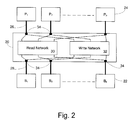
- FIG. 2 shows a schematic diagram of a read network and a write network forming an interconnection network for a shared memory system, constructed and operated in accordance with the principles of the present invention
- FIG. 3 shows the topology of a known type of interconnection network configured as a Baseline Network with eight ports at each side in accordance with the principles of the present invention
- FIG. 4 shows an example of the common topology of a read network and a write network based on logarithmic multistage networks
- FIG. 5 shows the aggregated variables that are input to the interconnection network, and the aggregated values computed as functions of these variables, wherein the network complies with the concept of a combinational system in accordance with a preferred embodiment of the present invention
- FIG. 6 shows the combinational interconnection network of FIG. 5 together with the processing cores and memory banks which produce the variables and use the values computed as functions of these variables;
- FIG. 7 shows the combinational interconnection network of FIG. 5 , but with a decomposition of the overall combinational system into combinational sub-blocks;
- FIG. 8 shows how a preferred embodiment of the present invention based on pipelining is obtained by adding pipeline registers
- FIG. 9 shows another preferred embodiment based on pipelining
- FIG. 10 shows yet another preferred embodiment based on pipelining
- FIG. 11 shows the binary representation of a memory address issued by a processing core
- FIG. 12 shows an example of a multipath with a tree topology that is formed inside the read network when there is a multicast of the contents of a memory address.
- FIG. 1 shows a generalized example of a prior art shared memory system comprising an interconnection network and memory banks connected, to multiple processor cores.
- the interconnection network 20 of FIG. 1 is conceived to be a complicated and cumbersome apparatus, which cannot provide bandwidth high enough and at the same time abide by latencies low enough so as to allow access to random addresses with efficiency comparable to that of a local memory.
- topology refers to the set of static connections between these components.
- the topology determines, for each component, which are the other components attached to it through a direct, fixed, physical connection.
- the topology may also determine the ports of the components that serve for the connections.
- the relevant set of components includes the basic building blocks of the network itself, namely switches and other basic elements that serve for routing, connection or bridging, as well as the elements attached to the external ports of the network.
- these external elements are the processing cores 24 (labeled P 1 , P 2 . . . P n ), connected at one side of the network, and the memory banks 22 (labeled B 1 , B 2 . . . Bk), connected at the opposite side.
- FIG. 2 shows a schematic diagram of a read network and a write network forming an interconnection network for a shared memory system, constructed and operated in accordance with the principles of the present invention.
- Interconnection Network 20 in a preferred embodiment of the present invention, is shown as constructed from two, smaller sub-networks: a Read Network 30 serving for reading from memory and a Write Network 32 serving for writing to memory that are connected in parallel.
- Interconnection Network 20 is represented by an outer box, and corresponds to the “Interconnection Network” box ( 20 ) in FIG. 1 as in the prior art.
- FIG. 2 also shows the outer ports 26 , 28 of the comprehensive network, with those ports 26 that are depicted at the top of FIG. 2 being intended to be connected to processing cores 24 , and those ports 28 that are depicted at the bottom being intended to be connected to memory banks 22 .
- the two inner boxes 30 , 32 represent the Read Network 30 and the Write Network 32 , respectively.
- the Read Network 30 serves for operations of reading from memory
- the Write Network 32 serves for operations of writing to memory.
- the black squares at the points of intersection between the ports 26 of Read Network 30 and those of Write Network 32 represent elements 34 of routing, connection or bridging. These elements 34 , when needed, are among the basic building blocks of an interconnection network.
- Interconnection Network 20 from separate read and write networks 30 , 32 that are connected in parallel as described above has the following advantage: the number of paths between processing cores 24 and memory banks 22 that the comprehensive Interconnection Network 20 can offer is increased, in comparison to a single network that undertakes both the read operations and the write operations. On the other hand, the overall amount of resources that are needed to implement the two sub-networks is not increased at the same proportion, because by being intended to transfer data only in one direction, each of the two sub-networks is simpler and more efficient than the alternative single network that transfers data both ways.
- the Interconnection Network 20 comprises only the read network 30 and does not contain a write network 32 .
- both the read network 30 and the write network 32 are constructed from even smaller sub-networks (whose topology is known by those skilled in the art).
- the distinction between read network 30 and write network 32 pertains only to the formation of paths, as explained hereinafter.
- the topology is concerned, there is no distinction between read network 30 and write network 32 , although this does not imply that the two networks must be identical: some parameters and choices can be set differently, as explained below.
- the common topology of read network 30 and of write network 32 is based on connecting a desired number m of sub-networks in parallel.
- the number m is later referred to as the “duplication factor”.
- the sub-networks are of the type known by those skilled in the art as “logarithmic multistage networks” (see FIG. 4 ), and the number of ports that they possess at each of their two sides is n, the number of processing cores.
- these logarithmic multistage networks are composed from uniform switches. Every path from one side of such a network to the opposite side passes through a series of switches of length equal to the logarithm according to base b of n, where b is the number of ports at each of the two sides of the switches.
- Two examples for logarithmic multistage networks that are known by those skilled in the art are the Omega Network and the Baseline Network.
- the Baseline Network is a generalized concept that is recognized in the prior art. It is known to those skilled in the art how to construct a Baseline Network with a given number of ports at each side, composed from switches whose number of ports at each side is also given.
- FIG. 3 there is shown a Baseline Network 40 topology with eight ports 42 at each side 43 , 44 , which is composed from switches 46 , each of which has two ports 47 at each side 48 .
- the ports at one side 43 of the network are labeled In_ 0 to In_ 7
- those at the other side 44 are labeled Out_ 0 to Out_ 7 .
- the numbers 0 to 7 serve here as indices.
- the network comprises three rows of switches 46 , which constitutes its basic building blocks. Every path from one of the external ports labeled In_ 0 to In_ 7 to one of the external ports labeled Out_ 0 to Out_ 7 at the other side of the network passes via one and only one switch 46 belonging to each of these three rows.
- the three rows are referred to as the three stages of the network.
- the following convention is adopted in the current figure: Ports through which initiatives that have originated at the processing cores 24 enter are labeled with names that contain the word “In”, while ports through which these initiatives exit on their way towards the memory banks 22 are labeled with names that contain the word “Out”; this applies for the ports of the network itself and for the ports of its building blocks alike.
- the reactions to the cores' initiatives travel in the opposite direction, though, and therefore each port, no matter whether its name contains the word “In” or the word “Out” typically includes both input and output signals.
- the common topology of read network 30 and of write network 32 is based on connecting m logarithmic multistage networks in parallel, with each of these m networks possessing n ports at each side.
- the parameter m which is referred to here and hereinafter as the “duplication factor”, assumes a desired value that is equal to or greater than one (m ⁇ 1); n being the number of processing cores 24 (see FIG. 2 ).
- FIG. 4 shows an example of the common topology of a read network and a write network based on logarithmic multistage networks.
- the Logarithmic Multistage Networks 54 possesses 8 ports that are indexed 0 to 7 at one side 50 (the side that is facing processing cores 24 ), and 16 ports that are indexed 0 to 15 at the other side 52 (the side that is facing memory banks 22 ).
- Four Logarithmic Multistage Networks 54 are connected in parallel in this example, namely the duplication factor m is 4. Every one of the four Logarithmic Multistage Networks 54 has n ports at each side.
- the black squares at the upper part of the figure as well as those at the lower part of the figure represent elements 34 a of routing, connection or bridging which are among the basic building blocks of an interconnection network.
- Every external port of the network is connected through an element 34 a of routing, connection or bridging, if it exists, to the corresponding port (the one that has the same index) of each one of the Logarithmic Multistage Networks 54 .
- every external port of the network is connected through element 34 a to (m ⁇ n)/k ports with successive indices of a Logarithmic Multistage Networks 54 ; in this example, every one of the 16 external ports depicted at the lower part of FIG. 4 is connected to two ports with successive indices of Logarithmic Multistage Networks 54 .
- the type of the logarithmic multistage networks may also vary. Yet in order for the topology to be proper it is necessary that the product of n and m will be equal to k or bigger than k, namely, in common mathematical notation, k ⁇ n ⁇ m.
- One other example for a possible set of values of the parameters which also represents a preferred embodiment of the present invention, is as follows: The number n of processing cores is 256, the value of the duplication factor m is 8 and the number k of memory banks is 512.
- the number k of memory banks 22 will not be smaller than the number n of processing cores 24 , namely n ⁇ k.
- the number n of processing cores 24 , the number k of memory banks 22 and the duplication factor m are whole powers of two.
- Another class of preferred embodiments is obtained from the former class by actually connecting less than n processing cores 24 (see FIG. 2 ) to the memory system, leaving a collection of processing cores 24 whose size is not a whole power of two, while retaining the original values of the number k of memory banks 22 (see FIG. 2 ) and of the duplication factor m.
- This reduction of the number of processing cores 24 may allow a limited reduction of the interconnection network 20 (see FIG. 2 ) as well.
- the memory system and its parameters do not undergo an essential change, because the number of ports of each of Logarithmic Multistage Networks 54 , at the side that is near memory banks 22 , remains the original number n.
- the advantage in having a greater value for the duplication factor m is that the number of paths between processing cores 24 and memory banks 22 is also increased.
- the value of the duplication factor m may differ between the read network 30 and the write network 32 (see FIG. 2 ), selecting an identical value has the following advantage: in a physical-geometrical implementation of the interconnection network 20 , the read network 30 and the write network 32 can be laid in parallel to each other, with every building block, such as switches 46 (see FIG. 3 ), and every link inside the read network 30 placed next to the corresponding building block or link of the write network 32 . Such a layout can be more area-efficient and wiring-efficient, as well as simpler to design.
- the memory system presented herein is based on dividing the time into intervals or slices known by those skilled in the art as “clock cycles”. The same common division of the time applies, within the context of a given memory system, to all the processing cores 24 (see FIG. 2 ) that are connected to the memory system, as well as to any timed resource within the memory system.
- Every processing core 24 is eligible for initiating one access to a memory address that belongs to the memory space embodied by the given memory system, at every clock cycle.
- the initiatives taken by processing cores 24 lead to a process of defining paths between processing cores 24 and memory banks 22 , via interconnection network 20 . This path definition process is performed anew, once at every clock cycle.
- the paths thus defined are not partial, but rather full paths that begin in processing cores 24 , traverse interconnection network 20 , and terminate in memory banks 22 .
- a processing core 24 (see FIG. 2 ) whose initiative is indeed fulfilled receives an approval reply, while a processing core 24 whose initiative is not fulfilled receives a rejection reply.
- a processing core 24 that receives a rejection reply typically retries to submit its initiative at a later clock cycle. The resubmission is done in the same way as the original submission, as though the latter did not take place at all.
- the activity that takes place in order to fulfill the simultaneous accessing of memory by numerous processing cores includes the following activity ingredients, labeled A to G:
- Ingredient B definition of paths between processing cores and memory banks in the interconnection network, which will carry contents signifying data, addresses and control;
- Ingredient C transfer of approval and rejection replies to those processing cores that initiated memory accesses
- Ingredient D reading from memory banks, pursuant to read initiatives
- Ingredient E transfer of contents that were read from memory banks to the processing cores that initiated the reading
- Ingredient F transfer of contents from those processing cores that initiated write operations to the memory banks wherein the writing should take place;
- Ingredient G writing to memory banks, pursuant to write initiatives.
- all the activity ingredients that stem from the same set of initiatives are performed at one clock cycle; in other words, the activity ingredients B, C, D, E, F and G are performed at the same clock cycle as the ingredient A from which they stem.
- the activity ingredients B, C, D, F and G are performed at the same clock cycle as ingredient A from which they stem; however, ingredient E is performed at the subsequent cycle, at which a fresh set of initiatives is already submitted.
- This second preferred embodiment is based on what is known by those skilled in the art as a “pipeline”.
- the advantage of pipelining is the potential shortening of the duration of the clock cycles.
- the number of pipeline stages is two in this second preferred embodiment of the present invention, as illustrated in the following diagram:
- Ingredient A submission of initiatives ⁇ Ingredient B: Definition of paths ⁇ Ingredient C: Approval/rejection replies ⁇ Ingredient D: Reading from memory ⁇ Ingredient E: Transfer of contents that were read ⁇ Ingredient F: Transfer of contents to write ⁇ Ingredient G: Writing to memory ⁇
- the activity ingredients B, D, F and G are performed at the same clock cycle as the ingredient A from which they stem; however, the two ingredients C and E are performed at the subsequent clock cycle.
- the third preferred embodiment is also based on two pipeline stages, the difference being in the apportionment of the activity between the pipeline stages. This is made clear using the diagram below, which pertains to the third preferred embodiment:
- Ingredient A submission of initiatives ⁇ Ingredient B: Definition of paths ⁇ Ingredient C: Approval/rejection replies ⁇ Ingredient D: Reading from memory ⁇ Ingredient E: Transfer of contents that were read ⁇ Ingredient F: Transfer of contents to write ⁇ Ingredient G: Writing to memory ⁇
- activity ingredients B, C and F are performed at the same clock cycle as ingredient A from which they stem; the two ingredients D and G are performed at a subsequent cycle, and the last ingredient E is performed one more cycle later.
- the following diagram illustrates the three pipeline stages of the fourth preferred embodiment:
- various preferred embodiments of the present invention may feature different pipeline configurations. Among these configurations there are included: the one on which the first preferred embodiment described above is based, where all the activity is performed at the same clock cycle so in fact there is no pipeline at all; the configurations with two pipeline stages on which the second and third preferred embodiments above are based; and the configuration with three pipeline stages on which the fourth preferred embodiment above is based. Additional pipeline configurations where the activity ingredients A to G are apportioned differently among the pipeline stages may give rise to additional preferred embodiments of the present invention.
- Different pipeline configurations may rely either on leaving the three stages (a), (b) and (c) as disjoint stages; or on unifying (a) and (b) into one stage so that altogether there remain two stages; or on unifying (b) and (c) into one stage so that here too there remain two stages; or on unifying the three stages (a), (b) and (c) into one stage, so that, in fact, no pipeline remains.
- the activity ingredients A, B and F always belong, according this scheme, to stage (a).
- the ingredients D and G always belong to stage (b).
- the ingredient E always belongs to stage (c).
- the activity ingredient C may belong according this scheme to either one of the three stages (a), (b) or (c).
- both the second and the third preferred embodiments are based on unifying the stages (a) and (b) into one stage. These two embodiments differ, however, in the stage at which the activity ingredient C is performed: In the second preferred embodiment it is stage (a) or (b), whereas in the third preferred embodiment it is stage (c).
- the interconnection network 20 (see FIG. 2 ) accepts the initiatives of the processing cores 24 plus signals generated by the memory banks 22 as input variables. From these variables interconnection network 20 computes the following functions f 1 to f 6 :
- f 1 the paths that should be defined between processing cores 24 and memory banks 22 , and are expressed in the switching states of the basic elements from which interconnection network 20 is built and;
- f 2 the data contents that should appear on the ports of various memory banks 22 , and which originate from write initiatives of processing cores 24 ;
- the computation of the functions f 1 to f 6 above does not depend on the state of the interconnection network 20 (see FIG. 2 ) in previous clock cycles.
- the interconnection network 20 complies with the concept of “combinational system”, known in the basic theory of digital systems.
- FIG. 5 shows the aggregated variables that are input to the interconnection network, and the aggregated values computed by the interconnection as functions of these variables, wherein the network complies with the concept of a combinational system in accordance with preferred embodiments of the present invention that are not based on pipelining.
- FIG. 5 there is depicted a combinational interconnection network 20 a as a single block that receives inputs 58 and generates outputs 60 .
- the outputs 60 indicated by f 1 to f 6 are functions of the current values of the inputs 58 , namely the variables x 1 and x 2 , provided that the system has been let enough time to stabilize.
- FIG. 6 depicts a combinational interconnection network 20 a as appearing in FIG. 5 , together with a collection 62 of processing cores 24 and a collection 64 of memory banks 22 , which produce the values of the variables x 1 and x 2 , which are aggregates of information, and use their functions f 1 to f 6 .
- the values of f 1 to f 6 whose meanings are defined hereinbefore, are also aggregates of information.
- the variable x 1 constitutes the initiatives of the collection 62 of processing cores 24
- the variable x 2 constitutes signals generated by the collection 64 of memory banks 22 . Note that FIG. 6 does not depict f 1 because it is used internally by the interconnection network itself.
- combinational interconnection network 20 Being a combinational system contributes to making combinational interconnection network 20 a simple, lean and light-weight. It also makes this inventive network fundamentally different from prior art interconnection networks which are arranged such that data, addresses and control values make a journey that may last multiple clock cycles from their processing cores to their memory banks or backwards.
- the light-weight combinational interconnection network 20 a presented in the framework of the present invention can be considered as similar to what is known by those skilled in the art as a “carry-look-ahead” adder: Both are combinational systems in which signal propagation delays depend logarithmically on the number of variables. A carry-look-ahead adder is considered a very compact and fast system.
- the function f 1 defined hereinbefore is still computed in its entirety from the variable x 1 introduced above, in a single clock cycle.
- all of the functions f 2 to f 6 are computed from x 1 , from the other variable x 2 introduced above and from f 1 (or from a subset of x 1 , x 2 and f 1 ), in a single clock cycle (which is the same cycle, when the interconnection is not based on pipelining).
- stage (a) of interconnection the transfer of the values of the the common scheme network to which functions f 2 , f 3 and f 4 defined above is not unified the memory banks above to the memory banks 22 with stage (b). 22 are attached. for one clock cycle.
- stage (b) of interconnection the transfer of the variables the common scheme network to which from which the function f 6 above is not unified the memory banks defined above is computed with stage (c). 22 are attached. from the memory banks 22 to the interconnection network for one clock cycle.
- any embodiment In an embodiment, in an embodiment with two based on pipelining. with two pipeline pipeline stages, this pipeline stages the register is register holds the value of the distributed all function f 1 defined above, as through the computed in the previous clock interconnection cycle.
- the basic building second among the two registers block of the holds the contents that the first network hosting a register held in the previous segment of the clock cycle, thus creating a register. delay of two cycles.
- a segment of this register that with three pipeline is hosted by a given building stages there are two block of the interconnection registers of this network contains information kind, connected one pertaining to the switching after the other. state of the same building block.
- this register (or of the second among the two registers in embodiments based on three pipeline stages) serve as variables of the function f 6 defined above.
- the contents of this register (or one of the two registers, in embodiments based on three pipeline stages) may also serve as variables of the function f 5 , depending on the pipeline stage where the activity ingredient C (described hereinbefore) is performed.
- FIG. 7 shows the combinational interconnection network of FIG. 5 , but with a decomposition of the overall combinational system into combinational sub-blocks.
- This first preferred embodiment among the four mentioned is not based on a pipeline, and thus the combinational interconnection network 20 a of this embodiment complies with FIG. 5 .
- the sub-blocks 66 , 68 , 70 , and 72 shown in FIG. 7 remain unbroken in any preferred embodiment of the present invention based on pipelining. Hence, the essentially combinational character of the interconnection network 20 a is preserved unharmed also in preferred embodiments that are based on pipelining.
- FIG. 8 shows how a preferred embodiment of the present invention based on pipelining is obtained by adding pipeline registers.
- the second preferred embodiment is based on two pipeline stages (the first being (a) unified with (b) and the second being (c)) and on performing the activity ingredient C in the first stage.
- pipeline registers 56 are implanted as shown in FIG. 8 , wherein they are symbolized by the black rectangles.
- Interconnection Network 20 b also comprises sub-blocks, 66 , 68 , 70 , and 72 .
- FIG. 9 shows third preferred embodiment, which differs from the second (shown in FIG. 8 ) only in the fact that here the activity ingredient C is performed in the second stage.
- Interconnection Network 20 c is also implanted with pipeline registers 56 and also comprises sub-blocks 66 , 68 , 70 , and 72 .
- FIG. 10 shows yet another preferred embodiment of the present invention based on pipelining.
- interconnection network 20 d is also provided with pipeline registers 56 implanted among sub-blocks 66 , 68 , 70 , and 72 as shown in FIG. 10 .
- sub-block 72 computes the function f 1 in each of the four preferred embodiments of interconnection network 20 a , 20 b , 20 c , and 20 d illustrated in FIGS. 7 through 10 .
- the number of pipeline stages in any pipelined system is known by those skilled in the art as the “pipeline depth”.
- the pipeline depth is two or three. Where there are no arrangements for pipelining, the pipeline depth is considered to be one.
- the small pipeline depth of up to three in the present invention helps to prevent or significantly reduce the frequency of stoppages, otherwise known as “stalls” in the operation of the processing cores 24 (see FIG. 2 ), which may occur when the memory system is pipelined. This is so because it is well known by those skilled in the art that the processing cores 24 themselves can be pipelined. What is needed is a match between the pipeline stages of the memory system and those of processing cores 24 . Namely, a processing core 24 should expect the outcome of its memory access initiative at the appropriate stage, one or two clock cycles later than the stage at which the initiative was taken.
- T forward T bridge1 +log b n*T in — to — out +T wire1
- T backward T bridge2 +log b n*T out — to — in +T wire2
- the delay times T forward and T backward are indeed sufficiently small:
- the components T bridge1 and T bridge2 depend only weakly on the number n of processing cores 24 , the number k of memory banks 22 and the duplication factor m.
- the components T in — to — out and T out — to — in have contributions that depend only on n, logarithmically, through the factor log b n; this contribution therefore stands in analogy with the delay of a carry-look-ahead adder, a combinational system that is considered very compact and fast.
- the contributions of the components T wire1 and T wire2 to the delay times T forward and T backward depend on cumulative lengths of wires, which do not exceed the length of a diagonal of a bounding rectangle.
- the paths in an interconnection network 20 are computed anew at every clock cycle. In this computation there is no need to take into account paths computed at earlier clock cycles; namely, there is no need to perform what is known by those skilled in the art as “rearrangement” of the paths. Another fact is that in determining the path between a processing core 24 and a memory bank 22 to which the processing core 24 initiates a reference, there is no need to take other processing cores' initiatives into account. There is only the need to return rejection replies when conflicts between paths occur as a result of a contest over ports of the interconnection network's building blocks. These two facts greatly simplify the computation of the paths, thereby helping the interconnection network 20 of the present invention to be simple, lean and light-weight.
- a path in the interconnection network 20 is computed from the memory address which the processing core 24 (see FIG. 2 ) submits, plus information about the type of access—whether it is a read or a write.
- this address unequivocally defines the following three items:
- the number n of processing cores 24 as well as the number k of memory banks 22 and the duplication factor m are whole powers of two. Also, the relation k ⁇ n ⁇ m or equivalently log 2 k ⁇ log 2 n +log 2 m holds true.
- the overall number of bits that are included in the binary representation of a memory address known by those skilled in the art as the “width of the address”, is determined by the desired size of the shared memory space. This width is typically larger than the sum log 2 n+log 2 m.
- the value of the duplication factor m is typically smaller than the value of the number k of memory banks 22 .
- FIG. 11 shows the binary representation of a memory address issued by a processing core 24 .
- the depiction in FIG. 11 of the representation of a binary memory address 80 issued by processing core 24 (as in FIG. 2 ) is used to explain the determination of items (i) (ii) and (iii) as defined heretofore.
- the most significant bit of the address is the leftmost bit, and the least significant is the rightmost.
- the log 2 k rightmost bits 84 where k is the number of memory banks 22 (see FIG. 2 ), are denoted Field A here.
- the remaining bits 86 are denoted Field B.
- the log 2 m rightmost bits 82 where m is the duplication factor, are denoted Field C
- the log 2 n bits 78 that are adjacent to Field C, where n is the number of processing cores are denoted Field D.
- the index of the memory bank 22 to which the reference is made is determined by the contents of Field A 84 of the address. Addresses that are adjacent or sufficiently close to one another differ only in the value of Field A 84 , and therefore such addresses are implemented in distinct memory banks.
- a program that is being run on a multicore computer typically tends to make their processing cores issue subsequent references to nearby addresses, according to what is known by those skilled in the art as “the principle of locality of reference”. Hence, such references tend to be scattered among distinct memory banks.
- This phenomenon which is known by those skilled in the art as “interleaving”, has the advantage of alleviating contests and conflicts.
- the conflicts relevant here are not related to paths in the interconnection network 20 (see FIG. 2 ) but rather to memory banks 22 (as in FIG. 2 ); however, these conflicts are nevertheless manifested and detected within the interconnection network 20 , at elements 34 , 34 a (see FIG. 2 , 4 ) thereof that are located at its perimeter, as explained further herein in the section entitled “Treating conflicts between paths”.
- the address inside that memory bank 22 (see FIG. 2 ) to which the reference is made is determined by Field B 86 of the address.
- the determination of the path includes:
- the three components (iii.1), (iii.2) and (iii.3) constitute together a full and unequivocal determination of the path inside the interconnection network 20 through which the access of the processing core 24 to a memory bank 22 is done. These three components are detailed in the following table.
- Component Details (iii.1) Determining This determination is done according to the whether the path information that the processing core 24 submits in passes through the conjunction with the memory address, regarding the read network 30 or type of requested access - whether it is a read or a the write network 32. write. (iii.2) Determining This determination is done according to the contents the logarithmic of Field C 82 of the address.
- the duplication multistage network factor m is larger than one, the interleaving 54 through which the phenomenon explained above in the context of path passes. scattering the references among different memory banks 22 occurs here too; the current context is the usage of different Logarithmic Multistage Networks 54.
- the interleaving phenomenon has the advantage of alleviating contests and conflicts related to paths in the interconnection network 20.
- logarithmic multistage network 54 Determining This determination is done according to the contents the internal path of Field D 78 of the address.
- the routing inside the inside the logarithmic logarithmic multistage network 54 is done multistage according to the inherent routing laws of a network 54.
- the inherent routing law is as follows: First, if the value of the rightmost bit of Field D 78 is ‘0’ then the path proceeds outwards of the first switch to which it entered via the port Out_0 of that switch; otherwise (namely the value is ‘1’), the path proceeds outwards via the port Out_1. Then, the path has to proceed through log 2 n ⁇ 1 further switches, which belong to the same number of further stages. The same rule that applied to the first switch continues to apply for these further switches, with the i th rightmost bit of Field D 78 of the address determining the routing at the i th switch, for every i between 2 and log 2 n.
- the internal routing inside a Baseline Network is based on using the bits of the relevant field of the address from right to left. In this way the less significant bits determine the routing at the earlier stages of the Baseline Network. This is done in order to achieve an interleaving effect:
- two addresses have identical contents in Field C 82, which means that they imply paths that use the same Logarithmic Multistage Network 54, it is still desirable to prevent a conflict between these two paths when the two addresses are relatively close to each other.
- Such relative closeness is expressed in an identity between the more significant bits of Field D 78 of the two addresses, while the less significant bits are non-identical.
- Each processing core 24 may take the initiative of accessing the shared memory at every clock cycle.
- the set of all initiatives submitted at a given clock cycle defines a corresponding set of requested paths between processing cores 24 and memory banks 22 .
- the memory system detects such conflicts, and reacts to them by performing activity differently in the read network 30 and in the write network 32 (see FIG. 2 ).
- the read network 30 is distinguished from the write network 32 in supporting multicast, which contributes to a reduction of the number of conflicts.
- the support of multicast in the read network 30 is explained further herein in the section entitled “Support of multicast for accommodating read-related hot spots.”
- the following description relates to the detection of conflicts and the provision of the reactions to them as performed by an interconnection network, excluding a read network.
- (I) A port of an internal switch of a Logarithmic Multistage Network 54 .
- the logarithmic multistage networks 54 are Baseline Networks composed from switches 46 with two ports at each side. This is an “Out_ 0 ” or an “Out_ 1 ” port (see FIG. 3 ).
- the conflict is detected locally at the switch or at the other basic network element, when two or more requests to acquire the same port thereof at the side 52 (see FIG. 4 ) closer to memory banks 22 (see FIG. 2 ) are placed. These requests arrive via different ports at the side 50 (see FIG. 4 ) that is closer to the processing cores 24 (see FIG. 2 ).
- the relevant element is a switch 46 that resides inside a Baseline Network and has two ports at each side
- two requests that arrive via the ports In_ 0 and In_ 1 may collide and create a conflict if both require the port Out_ 0 , or if both require the port Out_ 1 (see FIG. 3 ). From the explanation above it is clear that for such a collision to occur in this example, it is necessary (but not sufficient) that the relevant bit of Field D 78 of the address will be identical at the two memory addresses which serve as targets for access.
- a switch or another network element that detects a conflict takes a local decision to which of the conflicting incoming requests to grant the contested port.
- this decision relies only on fixed priorities assigned to the ports at the side closer to the processing cores 24 , through which the requests arrive; while being fixed with respect to time, these priorities may depend on the identity of the requested port at the side closer to memory banks 22 . This is a simple decision mechanism that contributes to the slenderness of the network.
- the switch or other network element exports an approval reply via the port (at the side closer to the processing cores 24 ) that serves the winning request. It also exports rejection replies via the ports (also at the side closer to the processing cores 24 ) that serve the other requests involved in the contest.
- a rejection reply can be generated locally at the network element only in the case of detecting a conflict.
- a rejection reply can also be exported as a result of being forwarded, rather than as a result of being generated locally.
- a forwarded rejection reply supersedes any approval reply that the current network element has generated.
- this rejection reply arrives at a network element via a port thereof at the side of the memory banks 22 that has been granted in response to a request, this rejection reply must be forwarded. And it must be forwarded via the port at the other side (namely the side of processing cores 24 ) through which the winning request comes.
- a trail of rejection replies can thus be created, which starts at a network element that detects a conflict and generates a rejection reply locally, and then propagates through other network elements that are ever closer to the processing cores 24 . Eventually the trail reaches the processing core 24 whose initiative is being rejected.
- a processing core 24 that receives a rejection reply typically resubmits its initiative at a later clock cycle.
- the submission of the initiative at the current clock cycle has brought about the allocation of an incomplete path inside the interconnection network 20 .
- This path is cut off at a network element which detects a conflict and takes a local decision to reject the submitted request.
- By occupying resources of the interconnection network 20 such an incomplete path may prevent the allocation of other paths and the fulfillment of other requests. Nevertheless, to keep the computation of the paths simple and fast, no reclaiming of the resources and no rearrangement of the paths are done.
- a second requirement that must be met in addition to the requirement discussed above concerning delays, is as follows: the number of paths between processing cores 24 and memory banks 22 that the interconnection network 20 can provide must be large enough. This requirement is not met when too many conflicts are created as a result of competition over the resources of the interconnection network 20 and over the memory banks 22 themselves.
- the analytical formula presented below is intended for a situation where the ratio between read and write operations is such that all the logarithmic multistage networks 54 contained in the interconnection network 20 are used with equal frequency, irrespective of whether they serve for reads or for writes. This removes the complication associated with the distinction between reads and writes, for the sake of simplicity of the analysis.
- a conflict is detected locally at a switch or at another basic element of the network, which identifies that there is more than one request to acquire the same port thereof, at the side that is closer to the memory banks 22 .
- the network element takes a local decision as to which among the colliding requests to grant the contested port.
- the network element may take a different type of reaction, based on checking the memory addresses which the colliding initiatives want to read.
- a multicast may take place, which is manifested as follows:
- the network element transfers the contents arriving from the direction of the memory banks 22 via the contested port to all the ports at its other side (namely the side closer to the processing cores 24 ) which carry initiatives that want to read from the relevant memory address.
- this relevant memory address is the one that is associated with the request that has the highest priority, and is selected according to the same simple selection scheme as described above for the rest of the network. In another preferred embodiment, this relevant memory address is the one that is associated with the maximal number of colliding requests.
- FIG. 12 shows an example of a multipath with a tree topology that is formed inside the read network when there is a multicast of the contents of a memory address.
- the multicast enables the reading of the same memory address at the same clock cycle by three processing cores 24 .
- the memory address resides within the memory bank 22 depicted in FIG. 12 .
- Multicast occurs here in read network 30 in two separate basic building blocks 88 which are labeled “Interconnection Element”. Building blocks 88 represent elements which may have functions similar to those of switches 46 (see FIG. 3 ) and basic elements 34 a (those that appear near the side 52 in FIG. 4 ), described heretofore.
- Each of these two interconnection elements represented by building blocks 88 receives, via ports at the side that is closer to the processing cores 24 , two requests to acquire the same port thereof at the other side in order to append this port to a path. While detecting the conflict, each of the two interconnection elements 88 also checks and finds that the two colliding requests were derived from read initiatives that pertain to the same memory address. Hence the multicast, whereby the interconnection element 88 transfers the contents arriving from the direction of the memory banks 22 via the contested port to two ports at the side closer to the processing cores 24 , rather than one. The multicast is decided at each interconnection element 88 locally, but creates an overall picture of a multi-path with a tree topology.
- the support of multicast in the read network 30 constitutes support for efficiently accommodating read-related hot spots.
Landscapes
- Engineering & Computer Science (AREA)
- Theoretical Computer Science (AREA)
- Physics & Mathematics (AREA)
- General Engineering & Computer Science (AREA)
- General Physics & Mathematics (AREA)
- Computer Hardware Design (AREA)
- Mathematical Physics (AREA)
- Software Systems (AREA)
- Multi Processors (AREA)
Abstract
Description
| First | Second | |
| Activity ingredient | stage | stage |
| Ingredient A: Submission of initiatives | ✓ | |
| Ingredient B: Definition of paths | ✓ | |
| Ingredient C: Approval/rejection replies | ✓ | |
| Ingredient D: Reading from memory | ✓ | |
| Ingredient E: Transfer of contents that were read | ✓ | |
| Ingredient F: Transfer of contents to write | ✓ | |
| Ingredient G: Writing to memory | ✓ | |
| First | Second | Third | |
| Activity ingredient | stage | stage | stage |
| Ingredient A: Submission of initiatives | ✓ | ||
| Ingredient B: Definition of paths | ✓ | ||
| Ingredient C: Approval/rejection replies | ✓ | ||
| Ingredient D: Reading from memory | ✓ | ||
| Ingredient E: Transfer of contents that were read | ✓ | ||
| Ingredient F: Transfer of contents to write | ✓ | ||
| Ingredient G: Writing to memory | ✓ | ||
| The preferred | ||
| embodiments | ||
| wherein the pipeline | Pipeline | |
| register is required | register's location | Pipeline register's role |
| Embodiments | At the end of the | This pipeline register hinders |
| wherein stage (a) of | interconnection | the transfer of the values of the |
| the common scheme | network to which | functions f2, f3 and f4 defined |
| above is not unified | the memory banks | above to the |
| with stage (b). | 22 are attached. | for one clock cycle. |
| Embodiments | At the end of the | This pipeline register hinders |
| wherein stage (b) of | interconnection | the transfer of the variables |
| the common scheme | network to which | from which the function f6 |
| above is not unified | the memory banks | defined above is computed |
| with stage (c). | 22 are attached. | from the |
| the interconnection network for | ||
| one clock cycle. | ||
| Any embodiment | In an embodiment | In an embodiment with two |
| based on pipelining. | with two pipeline | pipeline stages, this pipeline |
| stages the register is | register holds the value of the | |
| distributed all | function f1 defined above, as | |
| through the | computed in the previous clock | |
| interconnection | cycle. In an embodiment with | |
| network, with every | three pipeline stages, the | |
| basic building | second among the two registers | |
| block of the | holds the contents that the first | |
| network hosting a | register held in the previous | |
| segment of the | clock cycle, thus creating a | |
| register. | delay of two cycles. | |
| In an embodiment | A segment of this register that | |
| with three pipeline | is hosted by a given building | |
| stages there are two | block of the interconnection | |
| registers of this | network contains information | |
| kind, connected one | pertaining to the switching | |
| after the other. | state of the same building | |
| block. | ||
| The contents of this register (or | ||
| of the second among the two | ||
| registers in embodiments based | ||
| on three pipeline stages) serve | ||
| as variables of the function f6 | ||
| defined above. | ||
| The contents of this register (or | ||
| one of the two registers, in | ||
| embodiments based on three | ||
| pipeline stages) may also serve | ||
| as variables of the function f5, | ||
| depending on the pipeline stage | ||
| where the activity ingredient C | ||
| (described hereinbefore) is | ||
| performed. | ||
-
- 1) the combinational character of the interconnection network;
- 2) the number of switches along any path from side to side of the interconnection network depends logarithmically on the number n of processing cores, and
- 3) the useful property of a Baseline Network related to its physical-geometric layout on a planar surface in a manner that corresponds to
FIG. 3 , such that when it is bound within a rectangle, the maximal geometrical total length of any path from a port at one side of the Baseline Network to a port at the other side does not exceed the length of a diagonal of the bounding rectangle.
T forward =T bridge1+logb n*T in
where
- Tbridge1 is a delay time contributed by the
elements 34 of routing, connection or bridging that appear inFIG. 2 outside of the readnetwork 30 and thewrite network 32, and also theelements 34 a inFIG. 4 outside of theLogarithmic Multistage Networks 54; - Tin
— to— out is a delay time of a switch with b ports at each side, of the type from which the Logarithmic Multistage Nnetworks 54 (seeFIG. 4 ) are composed; - Twire1 is a signal propagation time through wires, including amplifiers or repeaters that may be located along these wires; and
- logbn stands for the logarithm according to base b of n, the number of processing cores 24 (see
FIG. 2 ).
T backward =T bridge2+logb n*T out
where
- Tbridge2 is a delay time contributed by the elements of routing, connection or bridging that appear in
FIG. 2 outside of the readnetwork 30 and thewrite network 32, and also inFIG. 4 outside of theLogarithmic Multistage Networks 54. The two values Tbridge2 and Tbridge1 are not necessarily equal; - Tout
— to— in is a delay time of a switch with b ports at each side, of the type from whichLogarithmic Multistage Networks 54 are composed. The two values Tout— to— in and Tin— to— out are not necessarily equal; and - Twire2 is a signal propagation time through wires, including amplifiers or repeaters that may be located along these wires. The two values Twire2 and Twire1 are not necessarily equal.
-
- (i) which
memory bank 22 is being accessed, and - (ii) what is the internal address inside that
memory bank 22, and in conjunction with the information about the type of access, the address unequivocally also defines: - (iii) the path in the
interconnection network 20 through which the access to memory is achieved.
- (i) which
k≦n×m
or equivalently
log2 k≦log2 n+log2 m
holds true. The overall number of bits that are included in the binary representation of a memory address, known by those skilled in the art as the “width of the address”, is determined by the desired size of the shared memory space. This width is typically larger than the sum log2n+log2m. The value of the duplication factor m is typically smaller than the value of the number k of
| Component | Details |
| (iii.1) Determining | This determination is done according to the |
| whether the path | information that the |
| passes through the | conjunction with the memory address, regarding the |
| | type of requested access - whether it is a read or a |
| the | write. |
| (iii.2) Determining | This determination is done according to the contents |
| the logarithmic | of |
| multistage network | factor m is larger than one, the |
| 54 through which the | phenomenon explained above in the context of |
| path passes. | scattering the references among |
| banks | |
| 22 occurs here too; the current context is the | |
| usage of different | |
| 54. Here the interleaving phenomenon has the | |
| advantage of alleviating contests and conflicts | |
| related to paths in the | |
| (iii.3) Determining | This determination is done according to the contents |
| the internal path | of |
| inside the logarithmic | logarithmic |
| multistage | according to the inherent routing laws of a |
| | logarithmic multistage network of the type chosen, |
| in order to achieve the following: The path that | |
| begins at the side that is closer to the processing | |
| cores 24 (see FIG. 4) should end at the other side | |
| (namely the side that is closer to the memory banks | |
| 22) at the port whose index is given by | |
| of the address. | |
| In a preferred embodiment of the present invention | |
| where the | |
| of the Baseline type, and they are composed from | |
| switches that have b = 2 ports at each side (see an | |
| example in FIG. 3), the inherent routing law is as | |
| follows: First, if the value of the rightmost bit of | |
| | |
| the first switch to which it entered via the port | |
| Out_0 of that switch; otherwise (namely the value is | |
| ‘1’), the path proceeds outwards via the port Out_1. | |
| Then, the path has to proceed through log2n − 1 | |
| further switches, which belong to the same number | |
| of further stages. The same rule that applied to the | |
| first switch continues to apply for these further | |
| switches, with the ith rightmost bit of | |
| the address determining the routing at the ith switch, | |
| for every i between 2 and log2n. | |
| In accordance with the present invention, the | |
| internal routing inside a Baseline Network is based | |
| on using the bits of the relevant field of the address | |
| from right to left. In this way the less significant | |
| bits determine the routing at the earlier stages of the | |
| Baseline Network. This is done in order to achieve | |
| an interleaving effect: When two addresses have | |
| identical contents in | |
| they imply paths that use the same | |
| Multistage Network | |
| 54, it is still desirable to | |
| prevent a conflict between these two paths when the | |
| two addresses are relatively close to each other. | |
| Such relative closeness is expressed in an identity | |
| between the more significant bits of | |
| the two addresses, while the less significant bits are | |
| non-identical. | |
| According to the routing law defined above, the two | |
| paths that are implied by the two relatively close | |
| addresses part from each other already at the early | |
| stages of the Baseline Network. In this way a | |
| conflict is prevented. | |
| When the multiplication product of the duplication | |
| factor m and the number n of | |
| greater than the number k of | |
| following happens: Each external port of the | |
| | |
| the side of the | |
| (through an | |
| bridging) to (m × n)/k consecutively indexed ports | |
| of a logarithmic multistage network 54 (see FIG. | |
| 4).. In such a situation there exist several different | |
| paths between a given | |
| given | |
| logarithmic | |
| of this kind serve for accessing two different | |
| address subspaces that are confined to the given | |
| | |
| characterization of such subspaces is the contents of | |
| the intersection between | |
| of the address. | |
Treating Conflicts Between Paths
-
- The first assumption is that the
processing cores 24 operate independently of each other. - The second assumption is that the probability that a
processing core 24 initiates a memory access at any clock cycle is given by some value p, which is uniform for all processingcores 24. (Hence, the probability that aprocessing core 24 does not initiate a memory reference at any given clock cycle is thecomplementary value 1−p.) - The third assumption is that any initiative to access memory may pertain to any memory address with the same probability.
- The first assumption is that the
where the meaning of the symbols is as follows:
-
- The symbol n stands for the number of processing cores.
- The symbol k stands for the number of memory banks.
- The symbol m stands for the number of logarithmic multistage networks contained in the interconnection network (in the current context there is no distinction made between the logarithmic multistage network contained in the read network and those that are contained in the write network).
- The symbol p stands for the probability that a processing core initiates a memory reference at any given clock cycle.
- The symbol f stands for the mathematical mapping which maps any real number x to the number f(x) given by the expression x−x2/4.
- The expression log2n appearing as an upper index indicates repetitive invocations, log2n times, of the mapping f.
Claims (17)
Priority Applications (1)
| Application Number | Priority Date | Filing Date | Title |
|---|---|---|---|
| US12/267,591 US8099561B2 (en) | 2007-11-09 | 2008-11-09 | Shared memory system for a tightly-coupled multiprocessor |
Applications Claiming Priority (2)
| Application Number | Priority Date | Filing Date | Title |
|---|---|---|---|
| US98665907P | 2007-11-09 | 2007-11-09 | |
| US12/267,591 US8099561B2 (en) | 2007-11-09 | 2008-11-09 | Shared memory system for a tightly-coupled multiprocessor |
Publications (2)
| Publication Number | Publication Date |
|---|---|
| US20090125685A1 US20090125685A1 (en) | 2009-05-14 |
| US8099561B2 true US8099561B2 (en) | 2012-01-17 |
Family
ID=40624833
Family Applications (1)
| Application Number | Title | Priority Date | Filing Date |
|---|---|---|---|
| US12/267,591 Active 2030-03-11 US8099561B2 (en) | 2007-11-09 | 2008-11-09 | Shared memory system for a tightly-coupled multiprocessor |
Country Status (7)
| Country | Link |
|---|---|
| US (1) | US8099561B2 (en) |
| EP (1) | EP2223219A4 (en) |
| JP (1) | JP2011503710A (en) |
| CN (1) | CN101855622A (en) |
| CA (1) | CA2705234A1 (en) |
| RU (1) | RU2010123391A (en) |
| WO (1) | WO2009060459A2 (en) |
Cited By (8)
| Publication number | Priority date | Publication date | Assignee | Title |
|---|---|---|---|---|
| US20110119553A1 (en) * | 2009-11-19 | 2011-05-19 | Lsi Corporation | Subwords coding using different encoding/decoding matrices |
| US20120117295A1 (en) * | 2010-11-09 | 2012-05-10 | Lsi Corporation | Multi-stage interconnection networks having fixed mappings |
| US8402324B2 (en) | 2010-09-27 | 2013-03-19 | Lsi Corporation | Communications system employing local and global interleaving/de-interleaving |
| US8588223B2 (en) | 2010-11-09 | 2013-11-19 | Lsi Corporation | Multi-stage interconnection networks having smaller memory requirements |
| US8621289B2 (en) | 2010-07-14 | 2013-12-31 | Lsi Corporation | Local and global interleaving/de-interleaving on values in an information word |
| US8976876B2 (en) | 2010-10-25 | 2015-03-10 | Lsi Corporation | Communications system supporting multiple sector sizes |
| US20150154114A1 (en) * | 2013-12-04 | 2015-06-04 | Lsi Corporation | System and method to interleave memory |
| US9514069B1 (en) | 2012-05-24 | 2016-12-06 | Schwegman, Lundberg & Woessner, P.A. | Enhanced computer processor and memory management architecture |
Families Citing this family (18)
| Publication number | Priority date | Publication date | Assignee | Title |
|---|---|---|---|---|
| US20090144476A1 (en) * | 2007-12-04 | 2009-06-04 | Xiaohua Cai | Hot plug in a link based system |
| FR2946441A1 (en) * | 2009-06-08 | 2010-12-10 | Commissariat Energie Atomique | NETWORK FOR INTERCONNECTIONS WITH DYNAMIC SUB-NETWORKS. |
| WO2011027302A1 (en) * | 2009-09-02 | 2011-03-10 | Plurality Ltd. | Associative distribution units for a high flow-rate synchronizer/scheduler |
| US20120210069A1 (en) * | 2009-10-25 | 2012-08-16 | Plurality Ltd. | Shared cache for a tightly-coupled multiprocessor |
| US20110161592A1 (en) * | 2009-12-31 | 2011-06-30 | Nachimuthu Murugasamy K | Dynamic system reconfiguration |
| US20110179311A1 (en) * | 2009-12-31 | 2011-07-21 | Nachimuthu Murugasamy K | Injecting error and/or migrating memory in a computing system |
| US9392143B1 (en) * | 2010-03-31 | 2016-07-12 | Ambarella, Inc. | High performance memory system for 3D color correction |
| CN103635875B (en) | 2011-03-25 | 2018-02-16 | 英特尔公司 | For by using by can subregion engine instance the memory segment that is performed come support code block of virtual core |
| TWI603198B (en) * | 2011-05-20 | 2017-10-21 | 英特爾股份有限公司 | Decentralized allocation of resources and interconnect structures to support the execution of instruction sequences by a plurality of engines |
| US9342394B2 (en) | 2011-12-29 | 2016-05-17 | Intel Corporation | Secure error handling |
| KR102083390B1 (en) | 2013-03-15 | 2020-03-02 | 인텔 코포레이션 | A method for emulating a guest centralized flag architecture by using a native distributed flag architecture |
| FR3025384B1 (en) * | 2014-09-03 | 2016-09-16 | Bull Sas | METHOD FOR MONITORING AND ROUTING CONFIGURATION ALERT IN A CLUSTER COMPRISING STATIC COMMUNICATION LINKS AND COMPUTER PROGRAM USING SAID METHOD |
| CN105760316B (en) * | 2014-12-19 | 2019-01-15 | 联想(北京)有限公司 | Control method device, connection matrix device, access method device and processing system |
| US9971711B2 (en) * | 2014-12-25 | 2018-05-15 | Intel Corporation | Tightly-coupled distributed uncore coherent fabric |
| US9690494B2 (en) * | 2015-07-21 | 2017-06-27 | Qualcomm Incorporated | Managing concurrent access to multiple storage bank domains by multiple interfaces |
| US11023277B2 (en) | 2016-09-20 | 2021-06-01 | Ramon Chips Ltd. | Scheduling of tasks in a multiprocessor device |
| CN109445680B (en) * | 2018-08-20 | 2020-03-31 | 华为技术有限公司 | Method and device for managing hard disk |
| CN115617718B (en) * | 2022-12-19 | 2023-03-21 | 芯动微电子科技(珠海)有限公司 | Read-write order-preserving method based on AXI bus and SoC system |
Citations (4)
| Publication number | Priority date | Publication date | Assignee | Title |
|---|---|---|---|---|
| US5202987A (en) | 1990-02-01 | 1993-04-13 | Nimrod Bayer | High flow-rate synchronizer/scheduler apparatus and method for multiprocessors |
| US6154816A (en) * | 1997-10-24 | 2000-11-28 | Compaq Computer Corp. | Low occupancy protocol for managing concurrent transactions with dependencies |
| US6301637B1 (en) * | 1998-06-08 | 2001-10-09 | Storage Technology Corporation | High performance data paths |
| US7673103B2 (en) * | 2004-06-04 | 2010-03-02 | Sun Microsystems, Inc. | Logging of level-two cache transactions into banks of the level-two cache stores the transactions for diagnostic and debug |
Family Cites Families (4)
| Publication number | Priority date | Publication date | Assignee | Title |
|---|---|---|---|---|
| KR0150072B1 (en) * | 1995-11-30 | 1998-10-15 | 양승택 | Device for controlling memory data path in parallel processing computer system |
| US6801985B1 (en) * | 1999-09-10 | 2004-10-05 | Texas Instruments Incorporated | Data bus using synchronous fixed latency loop including read address and data busses and write address and data busses |
| US7567567B2 (en) * | 2005-04-05 | 2009-07-28 | Sun Microsystems, Inc. | Network system including packet classification for partitioned resources |
| EP2383661A1 (en) * | 2005-04-21 | 2011-11-02 | Violin Memory, Inc. | Interconnection system |
-
2008
- 2008-11-09 JP JP2010532712A patent/JP2011503710A/en active Pending
- 2008-11-09 EP EP08847363A patent/EP2223219A4/en not_active Withdrawn
- 2008-11-09 RU RU2010123391/08A patent/RU2010123391A/en unknown
- 2008-11-09 US US12/267,591 patent/US8099561B2/en active Active
- 2008-11-09 CN CN200880115511A patent/CN101855622A/en active Pending
- 2008-11-09 CA CA2705234A patent/CA2705234A1/en not_active Abandoned
- 2008-11-09 WO PCT/IL2008/001474 patent/WO2009060459A2/en active Application Filing
Patent Citations (4)
| Publication number | Priority date | Publication date | Assignee | Title |
|---|---|---|---|---|
| US5202987A (en) | 1990-02-01 | 1993-04-13 | Nimrod Bayer | High flow-rate synchronizer/scheduler apparatus and method for multiprocessors |
| US6154816A (en) * | 1997-10-24 | 2000-11-28 | Compaq Computer Corp. | Low occupancy protocol for managing concurrent transactions with dependencies |
| US6301637B1 (en) * | 1998-06-08 | 2001-10-09 | Storage Technology Corporation | High performance data paths |
| US7673103B2 (en) * | 2004-06-04 | 2010-03-02 | Sun Microsystems, Inc. | Logging of level-two cache transactions into banks of the level-two cache stores the transactions for diagnostic and debug |
Non-Patent Citations (1)
| Title |
|---|
| "Computer Architecture-a Quantitative Approach" by John L. Hennessy and David A. Patterson, 2nd edition, p. 638. Published in San Francisco, 1996 by Morgan Kaufmann Publishers Inc. |
Cited By (13)
| Publication number | Priority date | Publication date | Assignee | Title |
|---|---|---|---|---|
| US20110119056A1 (en) * | 2009-11-19 | 2011-05-19 | Lsi Corporation | Subwords coding using different interleaving schemes |
| US8677209B2 (en) * | 2009-11-19 | 2014-03-18 | Lsi Corporation | Subwords coding using different encoding/decoding matrices |
| US20110119553A1 (en) * | 2009-11-19 | 2011-05-19 | Lsi Corporation | Subwords coding using different encoding/decoding matrices |
| US8423861B2 (en) | 2009-11-19 | 2013-04-16 | Lsi Corporation | Subwords coding using different interleaving schemes |
| US8621289B2 (en) | 2010-07-14 | 2013-12-31 | Lsi Corporation | Local and global interleaving/de-interleaving on values in an information word |
| US8402324B2 (en) | 2010-09-27 | 2013-03-19 | Lsi Corporation | Communications system employing local and global interleaving/de-interleaving |
| US8976876B2 (en) | 2010-10-25 | 2015-03-10 | Lsi Corporation | Communications system supporting multiple sector sizes |
| US8588223B2 (en) | 2010-11-09 | 2013-11-19 | Lsi Corporation | Multi-stage interconnection networks having smaller memory requirements |
| US20120117295A1 (en) * | 2010-11-09 | 2012-05-10 | Lsi Corporation | Multi-stage interconnection networks having fixed mappings |
| US8782320B2 (en) * | 2010-11-09 | 2014-07-15 | Lsi Corporation | Multi-stage interconnection networks having fixed mappings |
| US9514069B1 (en) | 2012-05-24 | 2016-12-06 | Schwegman, Lundberg & Woessner, P.A. | Enhanced computer processor and memory management architecture |
| US20150154114A1 (en) * | 2013-12-04 | 2015-06-04 | Lsi Corporation | System and method to interleave memory |
| US9208083B2 (en) * | 2013-12-04 | 2015-12-08 | Avago Technologies General Ip (Singapore) Pte. Ltd. | System and method to interleave memory |
Also Published As
| Publication number | Publication date |
|---|---|
| EP2223219A2 (en) | 2010-09-01 |
| WO2009060459A2 (en) | 2009-05-14 |
| RU2010123391A (en) | 2011-12-20 |
| JP2011503710A (en) | 2011-01-27 |
| CA2705234A1 (en) | 2009-05-14 |
| US20090125685A1 (en) | 2009-05-14 |
| CN101855622A (en) | 2010-10-06 |
| WO2009060459A3 (en) | 2010-03-11 |
| EP2223219A4 (en) | 2011-01-26 |
Similar Documents
| Publication | Publication Date | Title |
|---|---|---|
| US8099561B2 (en) | Shared memory system for a tightly-coupled multiprocessor | |
| US7251803B2 (en) | Memory re-implementation for field programmable gate arrays | |
| JPS62500902A (en) | Packet switched multiport memory N×M switch node and processing method | |
| CN104081722B (en) | Efficient peer-to-peer communications in SoC constructions are supported | |
| JPH07509085A (en) | Method and apparatus for unified parallel processing architecture | |
| Peh | Flow control and micro-architectural mechanisms for extending the performance of interconnection networks | |
| US8667199B2 (en) | Data processing apparatus and method for performing multi-cycle arbitration | |
| JP2731742B2 (en) | Parallel computer with cluster configuration | |
| Bhuyan | Analysis of interconnection networks with different arbiter designs | |
| US7574582B2 (en) | Processor array including delay elements associated with primary bus nodes | |
| CN105446935B (en) | It is shared to store concurrent access processing method and device | |
| KR20110066526A (en) | Multi-port memory controller and multi-port cache | |
| JP3990537B2 (en) | Hierarchical counterflow pipeline processor with advanced control | |
| JPH10333979A (en) | Bank access control system | |
| US10990408B1 (en) | Place and route aware data pipelining | |
| US7117321B2 (en) | System and method for interleaving SDRAM device access requests | |
| Raghunath | Interconnection network design based on packaging considerations | |
| JPS6125178B2 (en) | ||
| Juang et al. | Resource sharing interconnection networks in multiprocessors | |
| Brooks III | Performance of the butterfly processor-memory interconnection in a vector environment | |
| JP2555123B2 (en) | Memory access management method | |
| Dickey | Systolic combining switch designs | |
| Satpathy | High Performance and Low Power On-Die Interconnect Fabrics | |
| Dickey et al. | Interconnection network switch architectures and combining strategies | |
| Zuberek | Analysis of performance limitations in multithreaded multiprocessor architectures |
Legal Events
| Date | Code | Title | Description |
|---|---|---|---|
| AS | Assignment |
Owner name: PLURALITY LTD., ISRAEL Free format text: ASSIGNMENT OF ASSIGNORS INTEREST;ASSIGNORS:BAYER, NIMROD, MR.;PELEG, AVIELY, MR.;REEL/FRAME:022031/0073 Effective date: 20081224 |
|
| STCF | Information on status: patent grant |
Free format text: PATENTED CASE |
|
| FPAY | Fee payment |
Year of fee payment: 4 |
|
| MAFP | Maintenance fee payment |
Free format text: PAYMENT OF MAINTENANCE FEE, 8TH YR, SMALL ENTITY (ORIGINAL EVENT CODE: M2552); ENTITY STATUS OF PATENT OWNER: SMALL ENTITY Year of fee payment: 8 |
|
| AS | Assignment |
Owner name: N. B. PLURAL LTD., ISRAEL Free format text: ASSIGNMENT OF ASSIGNORS INTEREST;ASSIGNOR:PLURALITY LTD.;REEL/FRAME:049287/0383 Effective date: 20190527 |
|
| MAFP | Maintenance fee payment |
Free format text: PAYMENT OF MAINTENANCE FEE, 12TH YR, SMALL ENTITY (ORIGINAL EVENT CODE: M2553); ENTITY STATUS OF PATENT OWNER: SMALL ENTITY Year of fee payment: 12 |