US8102024B2 - Semiconductor integrated circuit and system LSI including the same - Google Patents

Semiconductor integrated circuit and system LSI including the same Download PDF

Info

Publication number
US8102024B2
US8102024B2 US12/883,546 US88354610A US8102024B2 US 8102024 B2 US8102024 B2 US 8102024B2 US 88354610 A US88354610 A US 88354610A US 8102024 B2 US8102024 B2 US 8102024B2
Authority
US
United States
Prior art keywords
polarity
diffusion layer
type diffusion
diode
type
Prior art date
Legal status (The legal status is an assumption and is not a legal conclusion. Google has not performed a legal analysis and makes no representation as to the accuracy of the status listed.)
Active
Application number
US12/883,546
Other versions
US20110001218A1 (en
Inventor
Shiro Usami
Current Assignee (The listed assignees may be inaccurate. Google has not performed a legal analysis and makes no representation or warranty as to the accuracy of the list.)
Socionext Inc
Original Assignee
Panasonic Corp
Priority date (The priority date is an assumption and is not a legal conclusion. Google has not performed a legal analysis and makes no representation as to the accuracy of the date listed.)
Filing date
Publication date
Application filed by Panasonic Corp filed Critical Panasonic Corp
Priority to US12/883,546 priority Critical patent/US8102024B2/en
Publication of US20110001218A1 publication Critical patent/US20110001218A1/en
Application granted granted Critical
Publication of US8102024B2 publication Critical patent/US8102024B2/en
Assigned to SOCIONEXT INC. reassignment SOCIONEXT INC. ASSIGNMENT OF ASSIGNORS INTEREST (SEE DOCUMENT FOR DETAILS). Assignors: PANASONIC CORPORATION
Active legal-status Critical Current
Anticipated expiration legal-status Critical

Links

Images

Classifications

    • HELECTRICITY
    • H01ELECTRIC ELEMENTS
    • H01LSEMICONDUCTOR DEVICES NOT COVERED BY CLASS H10
    • H01L29/00Semiconductor devices adapted for rectifying, amplifying, oscillating or switching, or capacitors or resistors with at least one potential-jump barrier or surface barrier, e.g. PN junction depletion layer or carrier concentration layer; Details of semiconductor bodies or of electrodes thereof  ; Multistep manufacturing processes therefor
    • H01L29/66Types of semiconductor device ; Multistep manufacturing processes therefor
    • H01L29/86Types of semiconductor device ; Multistep manufacturing processes therefor controllable only by variation of the electric current supplied, or only the electric potential applied, to one or more of the electrodes carrying the current to be rectified, amplified, oscillated or switched
    • H01L29/861Diodes
    • H01L29/8611Planar PN junction diodes
    • HELECTRICITY
    • H01ELECTRIC ELEMENTS
    • H01LSEMICONDUCTOR DEVICES NOT COVERED BY CLASS H10
    • H01L29/00Semiconductor devices adapted for rectifying, amplifying, oscillating or switching, or capacitors or resistors with at least one potential-jump barrier or surface barrier, e.g. PN junction depletion layer or carrier concentration layer; Details of semiconductor bodies or of electrodes thereof  ; Multistep manufacturing processes therefor
    • H01L29/40Electrodes ; Multistep manufacturing processes therefor
    • H01L29/41Electrodes ; Multistep manufacturing processes therefor characterised by their shape, relative sizes or dispositions
    • H01L29/417Electrodes ; Multistep manufacturing processes therefor characterised by their shape, relative sizes or dispositions carrying the current to be rectified, amplified or switched

Definitions

  • the present invention relates to improvements of a semiconductor integrated circuit including a diode and a system LSI.
  • FIG. 20 Insertion of these diode elements D 1 and D 2 can reduce the propagation of power supply noise and can ensure surge resistance to ESD.
  • a specific structure of such diode elements D 1 and D 2 provided for the purpose of reducing noise propagation is realized by MOS transistors as disclosed in, for example, Japanese Patent No. 2598147.
  • a desirable specific structure of the diode elements D 1 and D 2 is formed by gate-less diode elements instead of MOS transistors used in the conventional structure.
  • the diode element D shown in FIG. 21 includes, over a well 1 , a diffusion layer 5 which constitutes the anode and diffusion layers 4 provided on the left and right sides of the diffusion layer 5 which constitute the cathode. These diffusion layers 4 and 5 are both formed in a pattern of rectangular strips.
  • a well contact 2 is provided around the diffusion layers 4 and 5 constituting the anode and cathode to surround the diffusion layers 4 and 5 constituting the anode and cathode such that noise from the anode and cathode does not propagate to the outside.
  • the diffusion layers 4 and 5 constituting the anode and cathode and the well contact 2 are provided with a large number of contact holes 3 formed thereover for connection with the outside.
  • the above-described structure causes the following problem. Namely, since the diode element D shown in FIG. 21 is surrounded by the well contact 2 , a current flows from the diffusion layer 5 constituting the anode to neighboring part of the well contact 2 as illustrated by broken lines in FIG. 22 in addition to the current flowing from the diffusion layer 5 constituting the anode to the diffusion layers 4 constituting the cathode. In this case, it is expected that the current converges at contact holes 3 of the anode diffusion layer 5 in the vicinity of the well contact 2 to cause breakage of the contact holes 3 .
  • An objective of the present invention is to provide a semiconductor integrated circuit capable of producing a sufficient outcome with respect to its capacity as a protection device while preventing breakage and deterioration in reliability of a diode element.
  • the resistance between a diffusion layer constituting the anode of the diode element and a substrate or well contact in the vicinity of the diffusion layer is increased as illustrated in FIG. 23 such that the current toward the substrate or well contact is unlikely to flow.
  • a semiconductor integrated circuit of the present invention includes: a diode including a first polarity-type diffusion layer which constitutes an anode of the diode and a second polarity-type diffusion layer which is in the vicinity of the first polarity-type diffusion layer and which constitutes a cathode of the diode; and a second polarity-type substrate or well contact provided around the diode, wherein each of the first polarity-type diffusion layer and second polarity-type diffusion layer of the diode and the substrate or well contact has a plurality of contact holes for electrical connection with an external device, a positioning pitch of the plurality of contact holes of the second polarity-type substrate or well contact is greater than a positioning pitch of the plurality of contact holes of the first polarity-type diffusion layer which constitutes the anode of the diode.
  • An embodiment of a semiconductor integrated circuit of the present invention includes: a diode including a first polarity-type diffusion layer which constitutes an anode of the diode and a second polarity-type diffusion layer which faces the first polarity-type diffusion layer and which constitutes a cathode of the diode; and a second polarity-type substrate or well contact surrounding four sides of the diode, wherein each of the first polarity-type diffusion layer and second polarity-type diffusion layer of the diode has a plurality of contact holes for electrical connection with an external device, and the substrate or well contact has a plurality of contact holes except for a portion extending parallel to a direction in which the first polarity-type diffusion layer and the second polarity-type diffusion layer face each other.
  • the substrate or well contact has the plurality of contact holes only in a portion extending perpendicular to the direction in which the first polarity-type diffusion layer and the second polarity-type diffusion layer face each other.
  • a semiconductor integrated circuit of the present invention includes: a diode including a first polarity-type diffusion layer which constitutes an anode of the diode and a second polarity-type diffusion layer which faces the first polarity-type diffusion layer and which constitutes a cathode of the diode; and a second polarity-type substrate or well contact formed only by a portion extending perpendicular to a direction in which the first polarity-type diffusion layer and the second polarity-type diffusion layer face each other, wherein each of the first polarity-type diffusion layer and second polarity-type diffusion layer of the diode and the substrate or well contact has a plurality of contact holes for electrical connection with an external device.
  • a semiconductor integrated circuit of the present invention includes: a diode including a first polarity-type diffusion layer which constitutes an anode of the diode and a second polarity-type diffusion layer which faces the first polarity-type diffusion layer and which constitutes a cathode of the diode; and a second polarity-type substrate or well contact surrounding four sides of the diode, wherein each of the first polarity-type diffusion layer and second polarity-type diffusion layer of the diode and the substrate or well contact has a plurality of contact holes for electrical connection with an external device, a portion of the substrate or well contact extending parallel a direction in which the first polarity-type diffusion layer and the second polarity-type diffusion layer face each other has a greater separation from the first polarity-type diffusion layer or second polarity-type diffusion layer of the diode than a portion of the substrate or well contact extending perpendicular to the facing direction of the diffusion layers.
  • a positioning pitch of the plurality of contact holes of the second polarity-type substrate or well contact is greater than a positioning pitch of the plurality of contact holes of the first polarity-type diffusion layer which constitutes the anode of the diode.
  • the substrate or well contact has the plurality of contact holes except for a portion extending parallel to the direction in which the first polarity-type diffusion layer and the second polarity-type diffusion layer face each other.
  • the substrate or well contact has the plurality of contact holes only in a portion extending perpendicular to the direction in which the first polarity-type diffusion layer and the second polarity-type diffusion layer face each other.
  • a semiconductor integrated circuit of the present invention includes: a diode including a first polarity-type diffusion layer which constitutes an anode of the diode and a second polarity-type diffusion layer which faces the first polarity-type diffusion layer and which constitutes a cathode of the diode; and a second polarity-type substrate or well contact which shares a diffusion layer with the second polarity-type diffusion layer constituting the cathode of the diode and which surrounds four sides of the diode, wherein each of the first polarity-type diffusion layer and second polarity-type diffusion layer of the diode and the substrate or well contact has a plurality of contact holes for electrical connection with an external device, and a portion of the substrate or well contact extending parallel to a direction in which the first polarity-type diffusion layer and the second polarity-type diffusion layer face each other has a greater separation from the first polarity-type diffusion layer or second polarity-type diffusion layer of the diode than a portion of the
  • a positioning pitch of the plurality of contact holes of the second polarity-type substrate or well contact is greater than a positioning pitch of the plurality of contact holes of the first polarity-type diffusion layer which constitutes the anode of the diode.
  • the substrate or well contact has the plurality of contact holes except for a portion extending parallel to the direction in which the first polarity-type diffusion layer and the second polarity-type diffusion layer face each other.
  • the substrate or well contact has the plurality of contact holes only in a portion extending perpendicular to the direction in which the first polarity-type diffusion layer and the second polarity-type diffusion layer face each other.
  • the number of contact holes formed in the first polarity-type diffusion layer which constitutes the anode of the diode is equal to the number of contact holes formed in the second polarity-type diffusion layer which shares a diffusion layer with the second polarity-type substrate or well contact and which constitutes the cathode of the diode.
  • a semiconductor integrated circuit of the present invention includes: a diode including a first polarity-type diffusion layer which constitutes an anode of the diode and a second polarity-type diffusion layer which is in the vicinity of the first polarity-type diffusion layer and which constitutes a cathode of the diode; and a second polarity-type substrate or well contact, wherein the second polarity-type diffusion layer which constitutes the cathode of the diode substitutes for the second polarity-type substrate or well contact.
  • each of the first polarity-type diffusion layer of the diode and the second polarity-type diffusion layer of the diode which substitutes for the substrate or well contact has a plurality of contact holes for electrical connection with an external device, and the number of contact holes formed in the first polarity-type diffusion layer of the diode is equal to the number of contact holes formed in the second polarity-type diffusion layer of the diode which substitutes for the substrate or well contact.
  • the first polarity-type diffusion layer which constitutes the anode of the diode and the second polarity-type diffusion layer which constitutes the cathode of the diode have the shape of a rectangular strip.
  • the second polarity-type diffusion layer which constitutes the cathode of the diode is provided on both left and right sides of the first polarity-type diffusion layer which constitutes the anode of the diode.
  • a system LSI of the present invention includes: a digital circuit and an analog circuit which operate on separate power supplies; and a single unit of protection device formed by two aforementioned semiconductor integrated circuits and provided between the digital circuit and the analog circuit for allowing electrostatic discharge from the digital circuit to the analog circuit and electrostatic discharge from the analog circuit to the digital circuit.
  • the resistance value between a diffusion layer which constitutes the anode of the diode element and a substrate or well contact is increased. Accordingly, the current flowing from the diffusion layer which constitutes the anode of the diode element to the substrate or well contact decreases, and convergence of the current at contact holes formed in the anode is reduced. As a result, breakage and deterioration in reliability of the diode element can be effectively prevented. Further, the shape of the diffusion layer which constitutes the anode does not need to be additionally processed, for example, by truncation of four corners. Thus, it is not necessary to decrease the number of contact holes formed in the diffusion layer of the anode. Therefore, a sufficient outcome with respect to its capacity as a protection device can be produced.
  • the number of contact holes formed in the substrate or well contact does not need to be more than necessary. Thus, production becomes easy.
  • the current from the diffusion layer which constitutes the anode flows toward a diffusion layer of the cathode which faces the diffusion layer of the anode and also flows toward a portion of the substrate or well contact which extends parallel to the facing direction of the diffusion layers.
  • this portion of the substrate or well contact has a greater separation from the diffusion layers, so that the current is unlikely to flow toward this portion.
  • a portion of the substrate or well contact extending perpendicular to a direction in which the diffusion layers of the anode and cathode face each other has a smaller separation from the diffusion layer in the facing direction. Therefore, the area of the semiconductor integrated circuit is small as compared with a case where this separation in the facing direction is as large as the separation in the perpendicular direction, and hence, the size of the semiconductor integrated circuit is decreased.
  • the diffusion layer which constitutes the cathode of the diode share a diffusion layer with the substrate or well contact. Therefore, the space which occurs between the diffusion layer of the cathode and the substrate or well contact in the case where the diffusion layer is not shared can be reduced. Accordingly, the area of the semiconductor integrated circuit is decreased, and the size of the semiconductor integrated circuit is also decreased.
  • the diffusion layer which constitutes the cathode of the diode substitutes for the substrate or well contact. Therefore, the substrate or well contact is not necessary. Accordingly, the area of the semiconductor integrated circuit is decreased, and the size of the semiconductor integrated circuit is also decreased.
  • FIG. 1 shows a layout structure of a semiconductor integrated circuit according to Example 1 of the present invention.
  • FIG. 2 is a cross-sectional view of the semiconductor integrated circuit of Example 1.
  • FIG. 3 is a cross-sectional view of an alternative example of the semiconductor integrated circuit of Example 1.
  • FIG. 4 shows a layout structure of a semiconductor integrated circuit according to Variation 1 of Example 1.
  • FIG. 5 shows a layout structure of a semiconductor integrated circuit according to Variation 2 of Example 1.
  • FIG. 6 shows a layout structure of a modified version of the semiconductor integrated circuit according to Variation 2 of Example 1.
  • FIG. 7 shows a layout structure of a semiconductor integrated circuit according to Variation 3 of Example 1.
  • FIG. 8 shows a layout structure of a semiconductor integrated circuit according to Example 2 of the present invention.
  • FIG. 9 shows a layout structure of a modified version of the semiconductor integrated circuit according to Example 2.
  • FIG. 10 shows a layout structure of a semiconductor integrated circuit according to Variation 1 of Example 2.
  • FIG. 11 shows a layout structure of a semiconductor integrated circuit according to Variation 2 of Example 2.
  • FIG. 12 shows a layout structure of a semiconductor integrated circuit according to Variation 3 of Example 2.
  • FIG. 13 shows a layout structure of a semiconductor integrated circuit according to Example 3 of the present invention.
  • FIG. 14 shows a layout structure of a semiconductor integrated circuit according to Variation 1 of Example 3.
  • FIG. 15 shows a layout structure of a semiconductor integrated circuit according to Variation 2 of Example 3.
  • FIG. 16 shows a layout structure of a semiconductor integrated circuit according to Variation 3 of Example 3.
  • FIG. 17 shows a layout structure of a semiconductor integrated circuit according to Variation 4 of Example 3.
  • FIG. 18 shows a layout structure of a semiconductor integrated circuit according to Example 4 of the present invention.
  • FIG. 19 shows a layout structure of a semiconductor integrated circuit according to Variation 1 of Example 4.
  • FIG. 20 shows a place where a semiconductor integrated circuit of the present invention is applied.
  • FIG. 21 shows a proposed example of a semiconductor integrated circuit.
  • FIG. 22 is a schematic view illustrating the flow of currents in the layout structure of the semiconductor integrated circuit of the proposed example of FIG. 21 .
  • FIG. 23 is a schematic view illustrating the flow of currents in the layout structure of a semiconductor integrated circuit of the present invention.
  • Example 1 of the present invention a semiconductor integrated circuit according to Example 1 of the present invention is described with reference to FIG. 1 .
  • the place where the semiconductor integrated circuit of Example 1 as a protection device is applied is as previously described with reference to FIG. 20 , and therefore, the detailed description thereof is herein omitted.
  • FIG. 1 and FIG. 2 show the semiconductor integrated circuit of Example 1.
  • These drawings show a P-type (first polarity type) substrate B (shown only in FIG. 2 ) and an N-type (second polarity type) well 1 which is provided on the P-type substrate B.
  • a P-type diffusion layer (first polarity type diffusion layer) 5 which constitutes the anode is provided
  • two N-type diffusion layers (second polarity type diffusion layers) 4 which constitute the cathode are adjacently provided on opposite sides of the P-type diffusion layer 5 (on the left and right sides in the drawings).
  • These diffusion layers 4 and 5 constitute a diode D.
  • the P-type diffusion layer 5 which constitutes the anode and the N-type diffusion layers 4 which constitute the cathode are each has the shape of a rectangular strip in these drawings.
  • an N-type (second polarity type) well contact 2 having the shape of a rectangular frame surrounding the four sides of the diode D is provided.
  • the well contact 2 is provided for the purposes of preventing leakage of noise from the anode or cathode to the outside and preventing latch-up.
  • the diffusion layers 4 and 5 of the diode D and the well contact 2 have a large number of contact holes 3 over the entire region of each diffusion layer for connection with the outside and are connected from the contact holes 3 to the power supply or other semiconductor elements via signal lines 10 shown in FIG. 2 .
  • the positioning pitches of the contact holes 3 are “px” horizontally in the drawings and “py” vertically in the drawings (py>px).
  • the positioning pitch of the contact holes 3 is a setting pitch “pc”.
  • the setting pitch “pc” is greater than the maximum pitch of the contact holes 3 in the P-type diffusion layer 5 which constitutes the anode, i.e., the vertical positioning pitch “py” (pc>py).
  • the largeness of the current flowing through the diode D is determined by the number of contact holes 3 formed in the diffusion layers 5 and 4 which constitute the anode and cathode.
  • the shape of a rectangular strip is advantageous in determining the number of contact holes 3 to be provided. For example, if the number of contact holes 3 in the column direction is constant, the largeness of the current can be readily determined by changing the number of contact holes 3 in the row direction.
  • Example 1 the number of contact holes 3 formed in the N-type well 2 is small as compared with the proposed example shown in FIG. 21 .
  • the number of contact holes 3 of the N-type well 2 which are in the vicinity of the contact holes 3 formed along the edges of the P-type diffusion layer 5 which constitutes the anode is small, and the distance between the contact holes 3 of the N-type well 2 and the vicinal contact holes 3 of the P-type diffusion layer 5 is long. Accordingly, the value of resistance to the vicinal contact holes 3 is larger than the conventional resistance value.
  • the well 1 is of N-type
  • the diffusion layer 5 which constitutes the anode is of P-type
  • the diffusion layers 4 which constitute the cathode are of N-type, but the present invention is not limited thereto.
  • the conduction type of the well 1 may be P-type.
  • the anode and the cathode are replaced by each other.
  • an N-type diffusion layer 4 which constitute the cathode is placed at the center, while two P-type diffusion layers 5 which constitute the anode are provided on the left and right sides of the diffusion layer 4 , so that currents flow from the anode provided on the left and right sides to the cathode provided at the center.
  • Example 1 the substrate B has the well 1
  • the present invention is, as a matter of course, applicable to a substrate which does not have the well 1 .
  • the substrate B is of P-type
  • an N-type diffusion layer 4 which constitute the cathode is placed at the center
  • two P-type diffusion layers 5 which constitute the anode are provided on the left and right sides of the diffusion layer 4 .
  • the conduction type of the diffusion layer(s) which constitutes the anode and the diffusion layer(s) which constitutes the cathode may be changed variously so long as any one of the anode and cathode diffusion layers is of N-type while the other is of P-type.
  • the conduction type of any one of the anode and the cathode may be appropriately selected according to the conduction type of the well 2 or the conduction type of the substrate B.
  • the shape of the diffusion layers 4 and 5 constituting the anode and cathode is not limited to the rectangular strip.
  • FIG. 4 shows Variation 1 of Example 1.
  • FIG. 5 shows Variation 2 of Example 1.
  • Variation 2 of Example 1 is different from the semiconductor integrated circuit of FIG. 4 in that the contact holes 3 are not provided in the four corners of the rectangular well contact 2 . Therefore, a current from the diffusion layer 5 which constitutes the anode flows horizontally in the drawing to reach the diffusion layers 4 which constitute the cathode provided on the sides of the diffusion layer 5 . Thus, the current flowing from the diffusion layer 5 of the anode to the well contact 2 is further restricted, so that convergence of the current at contact holes 3 of the diffusion layer 5 of the anode which are in the vicinity of the well contact 2 is reduced. Hence, breakage and deterioration in reliability of the diode element can be effectively prevented.
  • the diffusion layers 4 and 5 of the diode D have the shape of a rectangular strip, but the present invention is not limited thereto.
  • the four corners of the strip-shaped diffusion layers 4 and 5 may be slightly truncated as illustrated in FIG. 6 .
  • FIG. 7 shows Variation 3 of Example 1.
  • the well contact 2 having the shape of a rectangular frame has a plurality of contact holes 3 only in portions which face the longer sides of the diffusion layers 4 constituting the cathode.
  • the upper and lower sides of the rectangular well contact 2 do not have the contact holes 3 .
  • Variation 3 of Example 1 As illustrated in FIG. 7 , the upper and lower sides of the rectangular well contact 2 which do not have the contact holes 3 are removed, such that the well contact 2 is formed only by the left and right side portions which face the longer sides of the diffusion layers 4 constituting the cathode.
  • Variation 3 of Example 1 the same functions and effects as those of Variation 2 of Example 1 are achieved.
  • Example 2 of the present invention is described with reference to FIG. 8 .
  • Example 2 is the same as the structure of FIG. 1 in that a P-type diffusion layer 5 which constitutes the anode of a diode D is provided at the center, while two diffusion layers 4 which constitute the cathode are provided on the left and right sides of the anode, and that the diode D is surrounded by a well contact 2 .
  • Example 2 portions of the well contact 2 extending parallel to a direction in which the diffusion layer 5 constituting the anode and the two diffusion layers 4 constituting the cathode face one another, i.e., the shorter side portions of the well contact 2 , has a greater separation from the diffusion layers 4 and 5 of the anode and cathode (separation tL) than portions of the rectangular well contact 2 extending perpendicular to the direction in which the diffusion layer 5 of the anode and the diffusion layers 4 of the cathode face one another, i.e., the longer side portions of the well contact 2 .
  • the positioning pitch of the contact holes 3 formed in the rectangular well contact 2 is equal to that of the contact holes 3 formed in the diffusion layers 4 and 5 of the anode and cathode.
  • separation tL between the diffusion layers 4 and 5 of the anode and cathode and the shorter side portions of the well contact 2 is longer than separation tS between the diffusion layers 4 of the cathode and the longer side portions of the well contact 2 (tL>tS).
  • the resistance value between the diffusion layer 5 of the anode and the shorter side portions of the well contact 2 is large.
  • the current flowing from the diffusion layer 5 of the anode to the shorter side portions of the well contact 2 is restricted, so that convergence of the current at contact holes 3 formed along the edges of the diffusion layer 5 of the anode which are in the vicinity of the well contact 2 is reduced.
  • breakage and deterioration in reliability of the diode D can be effectively prevented.
  • the diode D is formed by the diffusion layer 5 of the anode at the center and the two diffusion layers 4 of the cathode which are provided on the left and right sides of the diffusion layer 5 , but the present invention is not limited to this arrangement.
  • the diode D may have three diffusion layers 5 of the anode and four diffusion layers 4 of the cathode such that the diffusion layers 5 of the anode are provided alternately between the four diffusion layers 4 of the cathode. This also applies to the following descriptions.
  • FIG. 10 shows Variation 1 of Example 2.
  • FIG. 11 shows Variation 2 of Example 2.
  • Variation 2 of Example 2 provides the functions and effects of Variation 1 of Example 1 in addition to those of Example 2.
  • FIG. 12 shows Variation 3 of Example 2.
  • separation tL between the shorter side portions of the well contact 2 and the diffusion layers 5 and 4 of the anode and cathode is longer than separation tS between the longer side portions of the well contact 2 and the diffusion layers 4 of the cathode as in Example 2.
  • the well contact 2 has a plurality of contact holes 3 only in portions which face the longer sides of the diffusion layers 4 constituting the cathode.
  • Variation 3 of Example 2 provides the functions and effects of Variation 2 of Example 1 in addition to those of Example 2.
  • the well contact 2 has the shape of a rectangular frame
  • the shorter side portions of the well contact 2 may be omitted as in FIG. 7 because the shorter side portions do not have the contact holes 3 .
  • Example 3 of the present invention is described with reference to FIG. 13 .
  • Example 3 is the same as the structure of FIG. 1 in that a P-type diffusion layer 5 which constitutes the anode of a diode D is provided at the center, while two N-type diffusion layers 4 which constitute the cathode are provided on the left and right sides of the diffusion layer 5 of the anode, and that the diode D is surrounded by a well contact 2 .
  • Example 3 the rectangular well contact 2 is not separate from but shares a diffusion layer with the two N-type diffusion layers 4 which constitute the cathode. With this structure, the potential of the two N-type diffusion layers 4 which constitute the cathode of the diode D is equal to the potential of the well contact 2 .
  • Example 3 separation tL between the shorter side portions of the well contact 2 and the diffusion layers 5 and 4 of the anode and cathode is longer as in the semiconductor integrated circuit of Example 2 shown in FIG. 8 .
  • Example 3 shows in FIG. 13 , the space between the longer sides of the well contact 2 and the diffusion layers 4 of the cathode can be reduced as seen from comparison with FIG. 8 .
  • Example 3 provides the effect of reducing the area of the protection device in addition to the functions and effects of Example 2.
  • FIG. 14 shows Variation 1 of Example 3.
  • Variation 1 of Example 3 the longer side portions of the well contact 2 share a diffusion layer with the two N-type diffusion layers 4 constituting the cathode, and separation tL between the shorter side portions of the well contact 2 and the diffusion layers 5 and 4 of the anode and cathode is longer, as in Example 3 shown in FIG. 13 .
  • Variation 1 of Example 3 shown in FIG. 14 is the same as Example 1 of FIG. 1 in that the positioning pitch “pc” of the contact holes 3 formed in the well contact 2 is greater than the maximum pitch of the contact holes 3 in the P-type diffusion layer 5 which constitutes the anode, i.e., the vertical positioning pitch “py” (pc>py).
  • Variation 1 of Example 3 provides the functions and effects of Example 1 in addition to those of Example 3.
  • FIG. 15 shows Variation 2 of Example 3.
  • Variation 2 of Example 3 is different from Variation 1 of Example 3 in the following aspects.
  • the positioning pitch of the contact holes 3 formed in the well contact 2 is equal to the positioning pitch of the contact holes 3 of the diffusion layers 4 which constitute the cathode along the longer sides of the diffusion layers 4 as shown in FIG. 15 , although in Variation 1 of Example 3 the positioning pitch “pc” of the contact holes 3 formed in the well contact 2 is longer.
  • the shorter side portions of the well contact 2 do not have the contact holes 3 as shown in FIG. 4 of Variation 1 of Example 1.
  • Variation 2 of Example 3 provides the functions and effects of Variation 1 of Example 1 in addition to those of Example 3.
  • FIG. 16 shows Variation 3 of Example 3.
  • Variation 3 of Example 3 is different from Variation 2 of Example 3 shown in FIG. 15 in that parts of the longer side portions of the well contact 2 which do not face the diffusion layers 4 constituting the cathode do not have the contact holes 3 , and that the contact holes 3 are formed only in parts of the longer side portions of the well contact 2 which face the diffusion layers 4 constituting the cathode.
  • the other features of the structure are the same as those of FIG. 15 .
  • Variation 3 of Example 3 provides the functions and effects of Variation 2 of Example 1 in addition to those of Example 3.
  • FIG. 17 shows Variation 4 of Example 3.
  • Variation 4 of Example 3 is different from Variation 3 of Example 3 shown in FIG. 16 in that the longer side portions of the well contact 2 do not have the contact holes 3 .
  • the number of contact holes 3 of the diffusion layer 5 which constitutes the anode is equal to the total number of contact holes 3 of the two diffusion layers 4 which constitute the cathode.
  • the other features of the structure are the same as those of FIG. 16 .
  • the number of contact holes 3 of the diffusion layer 5 which constitutes the anode is equal to the number of contact holes 3 of the diffusion layers 4 which constitute the cathode. Accordingly, the current density in the anode is equal to the current density in the cathode. Therefore, the reliability of the diode D is improved.
  • Example 4 of the present invention is described with reference to FIG. 18 .
  • Example 4 as shown in FIG. 18 , a P-type diffusion layer 5 which constitutes the anode of a diode D is provided at the center, while two N-type diffusion layers 4 which constitute the cathode are provided on the left and right sides of the diffusion layer 5 of the anode.
  • Example 4 does not have a rectangular well contact surrounding the diode D. Instead, the two N-type diffusion layers 4 which constitute the cathode substitute for the well contact.
  • Example 4 Since in Example 4 an exclusive well contact is not provided, all of currents from the diffusion layer 5 which constitutes the anode infallibly flow into the diffusion layers 4 which constitute the cathode. Namely, the current flow from the diffusion layer 5 of the anode to the well contact, which would occur in the conventionally-proposed example, does not occur. Thus, convergence of the current at contact holes 3 of the diffusion layer 5 of the anode is infallibly reduced. Therefore, breakage and deterioration in reliability of the diode D can be prevented. Further, in Example 4, the area of the semiconductor integrated circuit is effectively reduced by omission of the exclusive well contact.
  • FIG. 19 shows Variation 1 of Example 4.
  • the semiconductor integrated circuit does not have an exclusive well contact. Instead, the two N-type diffusion layers 4 which constitute the cathode substitute for the well contact. Further, the number of contact holes 3 of the diffusion layer 5 which constitutes the anode is equal to the total number of contact holes 3 of the diffusion layers 4 which constitute the cathode.

Abstract

A semiconductor integrated circuit having a diode element includes a diffusion layer which constitutes the anode and two diffusion layers which are provided on the left and right sides of the anode and which constitute the cathode, such that the anode and the cathode constitute the diode. A well contact is provided to surround both the diffusion layers of the anode and cathode. Distance tS between a longer side of the well contact and the diffusion layers of the cathode is shorter, while distance tL between a shorter side of the well contact and the diffusion layers of the anode and cathode is longer (tL>tS). Accordingly, the resistance value between the diffusion layer of the anode and the shorter side of the well contact is larger, so that the current from the diffusion layer of the anode is unlikely to flow toward the shorter side of the well contact. Thus, convergence of the current at the contact holes of the diffusion layer of the anode is reduced, so that the reliability of the diode element improves.

Description

CROSS-REFERENCE TO RELATED APPLICATIONS
This Non-provisional application is a Divisional of U.S. patent application Ser. No. 11/783,133, filed on Apr. 6, 2007, now U.S. Pat. No. 7,821,096 and claims priority under 35 U.S.C. §119(a) on Patent Application No. 2006-124110 filed in Japan on Apr. 27, 2006, the entire contents of which are hereby incorporated by reference.
BACKGROUND OF THE INVENTION
The present invention relates to improvements of a semiconductor integrated circuit including a diode and a system LSI.
In recent years, development of system LSIs having higher functions has entailed coexistence of a plurality of digital circuit blocks and a plurality of analog circuit blocks in one chip. This configuration produces such a problem that noise from the digital circuit blocks propagates to the analog circuit blocks. To avoid this in the system LSI, the power supply of the digital circuit blocks and the power supply of the analog circuit blocks are separate from each other. However, for the purpose of protection against damage due to electro static discharge (ESD), a single unit of protection device formed by a pair of diodes D1. and D2 placed in opposite directions is inserted between the power supply of the digital circuit blocks and the power supply of the analog circuit blocks as shown in
FIG. 20. Insertion of these diode elements D1 and D2 can reduce the propagation of power supply noise and can ensure surge resistance to ESD.
A specific structure of such diode elements D1 and D2 provided for the purpose of reducing noise propagation is realized by MOS transistors as disclosed in, for example, Japanese Patent No. 2598147.
With respect to reduction in area, a desirable specific structure of the diode elements D1 and D2 is formed by gate-less diode elements instead of MOS transistors used in the conventional structure.
A proposed structure of such a diode element is, for example, one shown in FIG. 21. The diode element D shown in FIG. 21 includes, over a well 1, a diffusion layer 5 which constitutes the anode and diffusion layers 4 provided on the left and right sides of the diffusion layer 5 which constitute the cathode. These diffusion layers 4 and 5 are both formed in a pattern of rectangular strips. Around the diffusion layers 4 and 5 constituting the anode and cathode, a well contact 2 is provided to surround the diffusion layers 4 and 5 constituting the anode and cathode such that noise from the anode and cathode does not propagate to the outside. The diffusion layers 4 and 5 constituting the anode and cathode and the well contact 2 are provided with a large number of contact holes 3 formed thereover for connection with the outside.
When a surge voltage is applied to such a diode element D, a current is allowed to flow from the diffusion layer 5 constituting the anode to the diffusion layers 4 constituting the cathode as illustrated by solid lines in FIG. 22, whereby the diode element D is discharged and absorbs the surge voltage.
However, it was found that the above-described structure causes the following problem. Namely, since the diode element D shown in FIG. 21 is surrounded by the well contact 2, a current flows from the diffusion layer 5 constituting the anode to neighboring part of the well contact 2 as illustrated by broken lines in FIG. 22 in addition to the current flowing from the diffusion layer 5 constituting the anode to the diffusion layers 4 constituting the cathode. In this case, it is expected that the current converges at contact holes 3 of the anode diffusion layer 5 in the vicinity of the well contact 2 to cause breakage of the contact holes 3.
Such an undesirable result might be avoided by employing such a structure that, for example, the four corners of the diffusion layer 5 constituting the anode are truncated, and the contact holes 3 of the diffusion layer 5 are located distant from the four corners, such that electric field convergence at the corners is reduced. However, on the other hand, this structure would result in a smaller number of contact holes. Since the largeness of the current which flows through the diode element is limited by the number of contact holes, the diode element cannot produce a sufficient outcome with respect to its capacity as a protection device. This especially matters in microstructure processes performed with small contact hole diameters.
SUMMARY OF THE INVENTION
An objective of the present invention is to provide a semiconductor integrated circuit capable of producing a sufficient outcome with respect to its capacity as a protection device while preventing breakage and deterioration in reliability of a diode element.
To achieve the objective, according to the present invention, the resistance between a diffusion layer constituting the anode of the diode element and a substrate or well contact in the vicinity of the diffusion layer is increased as illustrated in FIG. 23 such that the current toward the substrate or well contact is unlikely to flow.
Specifically, a semiconductor integrated circuit of the present invention includes: a diode including a first polarity-type diffusion layer which constitutes an anode of the diode and a second polarity-type diffusion layer which is in the vicinity of the first polarity-type diffusion layer and which constitutes a cathode of the diode; and a second polarity-type substrate or well contact provided around the diode, wherein each of the first polarity-type diffusion layer and second polarity-type diffusion layer of the diode and the substrate or well contact has a plurality of contact holes for electrical connection with an external device, a positioning pitch of the plurality of contact holes of the second polarity-type substrate or well contact is greater than a positioning pitch of the plurality of contact holes of the first polarity-type diffusion layer which constitutes the anode of the diode.
An embodiment of a semiconductor integrated circuit of the present invention includes: a diode including a first polarity-type diffusion layer which constitutes an anode of the diode and a second polarity-type diffusion layer which faces the first polarity-type diffusion layer and which constitutes a cathode of the diode; and a second polarity-type substrate or well contact surrounding four sides of the diode, wherein each of the first polarity-type diffusion layer and second polarity-type diffusion layer of the diode has a plurality of contact holes for electrical connection with an external device, and the substrate or well contact has a plurality of contact holes except for a portion extending parallel to a direction in which the first polarity-type diffusion layer and the second polarity-type diffusion layer face each other.
In one embodiment of a semiconductor integrated circuit of the present invention, the substrate or well contact has the plurality of contact holes only in a portion extending perpendicular to the direction in which the first polarity-type diffusion layer and the second polarity-type diffusion layer face each other.
A semiconductor integrated circuit of the present invention includes: a diode including a first polarity-type diffusion layer which constitutes an anode of the diode and a second polarity-type diffusion layer which faces the first polarity-type diffusion layer and which constitutes a cathode of the diode; and a second polarity-type substrate or well contact formed only by a portion extending perpendicular to a direction in which the first polarity-type diffusion layer and the second polarity-type diffusion layer face each other, wherein each of the first polarity-type diffusion layer and second polarity-type diffusion layer of the diode and the substrate or well contact has a plurality of contact holes for electrical connection with an external device.
A semiconductor integrated circuit of the present invention includes: a diode including a first polarity-type diffusion layer which constitutes an anode of the diode and a second polarity-type diffusion layer which faces the first polarity-type diffusion layer and which constitutes a cathode of the diode; and a second polarity-type substrate or well contact surrounding four sides of the diode, wherein each of the first polarity-type diffusion layer and second polarity-type diffusion layer of the diode and the substrate or well contact has a plurality of contact holes for electrical connection with an external device, a portion of the substrate or well contact extending parallel a direction in which the first polarity-type diffusion layer and the second polarity-type diffusion layer face each other has a greater separation from the first polarity-type diffusion layer or second polarity-type diffusion layer of the diode than a portion of the substrate or well contact extending perpendicular to the facing direction of the diffusion layers.
In one embodiment of a semiconductor integrated circuit of the present invention, a positioning pitch of the plurality of contact holes of the second polarity-type substrate or well contact is greater than a positioning pitch of the plurality of contact holes of the first polarity-type diffusion layer which constitutes the anode of the diode.
In one embodiment of a semiconductor integrated circuit of the present invention, the substrate or well contact has the plurality of contact holes except for a portion extending parallel to the direction in which the first polarity-type diffusion layer and the second polarity-type diffusion layer face each other.
In one embodiment of a semiconductor integrated circuit of the present invention, the substrate or well contact has the plurality of contact holes only in a portion extending perpendicular to the direction in which the first polarity-type diffusion layer and the second polarity-type diffusion layer face each other.
A semiconductor integrated circuit of the present invention includes: a diode including a first polarity-type diffusion layer which constitutes an anode of the diode and a second polarity-type diffusion layer which faces the first polarity-type diffusion layer and which constitutes a cathode of the diode; and a second polarity-type substrate or well contact which shares a diffusion layer with the second polarity-type diffusion layer constituting the cathode of the diode and which surrounds four sides of the diode, wherein each of the first polarity-type diffusion layer and second polarity-type diffusion layer of the diode and the substrate or well contact has a plurality of contact holes for electrical connection with an external device, and a portion of the substrate or well contact extending parallel to a direction in which the first polarity-type diffusion layer and the second polarity-type diffusion layer face each other has a greater separation from the first polarity-type diffusion layer or second polarity-type diffusion layer of the diode than a portion of the substrate or well contact extending perpendicular to the facing direction of the diffusion layers.
In one embodiment of a semiconductor integrated circuit of the present invention, a positioning pitch of the plurality of contact holes of the second polarity-type substrate or well contact is greater than a positioning pitch of the plurality of contact holes of the first polarity-type diffusion layer which constitutes the anode of the diode.
In one embodiment of a semiconductor integrated circuit of the present invention, the substrate or well contact has the plurality of contact holes except for a portion extending parallel to the direction in which the first polarity-type diffusion layer and the second polarity-type diffusion layer face each other.
In one embodiment of a semiconductor integrated circuit of the present invention, the substrate or well contact has the plurality of contact holes only in a portion extending perpendicular to the direction in which the first polarity-type diffusion layer and the second polarity-type diffusion layer face each other.
In one embodiment of a semiconductor integrated circuit of the present invention, the number of contact holes formed in the first polarity-type diffusion layer which constitutes the anode of the diode is equal to the number of contact holes formed in the second polarity-type diffusion layer which shares a diffusion layer with the second polarity-type substrate or well contact and which constitutes the cathode of the diode.
A semiconductor integrated circuit of the present invention includes: a diode including a first polarity-type diffusion layer which constitutes an anode of the diode and a second polarity-type diffusion layer which is in the vicinity of the first polarity-type diffusion layer and which constitutes a cathode of the diode; and a second polarity-type substrate or well contact, wherein the second polarity-type diffusion layer which constitutes the cathode of the diode substitutes for the second polarity-type substrate or well contact.
In one embodiment of a semiconductor integrated circuit of the present invention, each of the first polarity-type diffusion layer of the diode and the second polarity-type diffusion layer of the diode which substitutes for the substrate or well contact has a plurality of contact holes for electrical connection with an external device, and the number of contact holes formed in the first polarity-type diffusion layer of the diode is equal to the number of contact holes formed in the second polarity-type diffusion layer of the diode which substitutes for the substrate or well contact.
In one embodiment of a semiconductor integrated circuit of the present invention, the first polarity-type diffusion layer which constitutes the anode of the diode and the second polarity-type diffusion layer which constitutes the cathode of the diode have the shape of a rectangular strip.
In one embodiment of a semiconductor integrated circuit of the present invention, the second polarity-type diffusion layer which constitutes the cathode of the diode is provided on both left and right sides of the first polarity-type diffusion layer which constitutes the anode of the diode.
A system LSI of the present invention includes: a digital circuit and an analog circuit which operate on separate power supplies; and a single unit of protection device formed by two aforementioned semiconductor integrated circuits and provided between the digital circuit and the analog circuit for allowing electrostatic discharge from the digital circuit to the analog circuit and electrostatic discharge from the analog circuit to the digital circuit.
Thus, in a semiconductor integrated circuit and system LSI of the present invention, the resistance value between a diffusion layer which constitutes the anode of the diode element and a substrate or well contact is increased. Accordingly, the current flowing from the diffusion layer which constitutes the anode of the diode element to the substrate or well contact decreases, and convergence of the current at contact holes formed in the anode is reduced. As a result, breakage and deterioration in reliability of the diode element can be effectively prevented. Further, the shape of the diffusion layer which constitutes the anode does not need to be additionally processed, for example, by truncation of four corners. Thus, it is not necessary to decrease the number of contact holes formed in the diffusion layer of the anode. Therefore, a sufficient outcome with respect to its capacity as a protection device can be produced.
Especially, according to the present invention, the number of contact holes formed in the substrate or well contact does not need to be more than necessary. Thus, production becomes easy.
According to the present invention, in the diode, the current from the diffusion layer which constitutes the anode flows toward a diffusion layer of the cathode which faces the diffusion layer of the anode and also flows toward a portion of the substrate or well contact which extends parallel to the facing direction of the diffusion layers. However, this portion of the substrate or well contact has a greater separation from the diffusion layers, so that the current is unlikely to flow toward this portion. Herein, a portion of the substrate or well contact extending perpendicular to a direction in which the diffusion layers of the anode and cathode face each other has a smaller separation from the diffusion layer in the facing direction. Therefore, the area of the semiconductor integrated circuit is small as compared with a case where this separation in the facing direction is as large as the separation in the perpendicular direction, and hence, the size of the semiconductor integrated circuit is decreased.
Further, according to the present invention, the diffusion layer which constitutes the cathode of the diode share a diffusion layer with the substrate or well contact. Therefore, the space which occurs between the diffusion layer of the cathode and the substrate or well contact in the case where the diffusion layer is not shared can be reduced. Accordingly, the area of the semiconductor integrated circuit is decreased, and the size of the semiconductor integrated circuit is also decreased.
In addition, according to the present invention, the diffusion layer which constitutes the cathode of the diode substitutes for the substrate or well contact. Therefore, the substrate or well contact is not necessary. Accordingly, the area of the semiconductor integrated circuit is decreased, and the size of the semiconductor integrated circuit is also decreased.
BRIEF DESCRIPTION OF THE DRAWINGS
FIG. 1 shows a layout structure of a semiconductor integrated circuit according to Example 1 of the present invention.
FIG. 2 is a cross-sectional view of the semiconductor integrated circuit of Example 1.
FIG. 3 is a cross-sectional view of an alternative example of the semiconductor integrated circuit of Example 1.
FIG. 4 shows a layout structure of a semiconductor integrated circuit according to Variation 1 of Example 1.
FIG. 5 shows a layout structure of a semiconductor integrated circuit according to Variation 2 of Example 1.
FIG. 6 shows a layout structure of a modified version of the semiconductor integrated circuit according to Variation 2 of Example 1.
FIG. 7 shows a layout structure of a semiconductor integrated circuit according to Variation 3 of Example 1.
FIG. 8 shows a layout structure of a semiconductor integrated circuit according to Example 2 of the present invention.
FIG. 9 shows a layout structure of a modified version of the semiconductor integrated circuit according to Example 2.
FIG. 10 shows a layout structure of a semiconductor integrated circuit according to Variation 1 of Example 2.
FIG. 11 shows a layout structure of a semiconductor integrated circuit according to Variation 2 of Example 2.
FIG. 12 shows a layout structure of a semiconductor integrated circuit according to Variation 3 of Example 2.
FIG. 13 shows a layout structure of a semiconductor integrated circuit according to Example 3 of the present invention.
FIG. 14 shows a layout structure of a semiconductor integrated circuit according to Variation 1 of Example 3.
FIG. 15 shows a layout structure of a semiconductor integrated circuit according to Variation 2 of Example 3.
FIG. 16 shows a layout structure of a semiconductor integrated circuit according to Variation 3 of Example 3.
FIG. 17 shows a layout structure of a semiconductor integrated circuit according to Variation 4 of Example 3.
FIG. 18 shows a layout structure of a semiconductor integrated circuit according to Example 4 of the present invention.
FIG. 19 shows a layout structure of a semiconductor integrated circuit according to Variation 1 of Example 4.
FIG. 20 shows a place where a semiconductor integrated circuit of the present invention is applied.
FIG. 21 shows a proposed example of a semiconductor integrated circuit.
FIG. 22 is a schematic view illustrating the flow of currents in the layout structure of the semiconductor integrated circuit of the proposed example of FIG. 21.
FIG. 23 is a schematic view illustrating the flow of currents in the layout structure of a semiconductor integrated circuit of the present invention.
DESCRIPTION OF THE PREFERRED EMBODIMENTS
Hereinafter, examples of the present invention will be described with reference to the drawings.
EXAMPLE 1
Hereinafter, a semiconductor integrated circuit according to Example 1 of the present invention is described with reference to FIG. 1. The place where the semiconductor integrated circuit of Example 1 as a protection device is applied is as previously described with reference to FIG. 20, and therefore, the detailed description thereof is herein omitted.
FIG. 1 and FIG. 2 show the semiconductor integrated circuit of Example 1. These drawings show a P-type (first polarity type) substrate B (shown only in FIG. 2) and an N-type (second polarity type) well 1 which is provided on the P-type substrate B. In the N-type well 1, a P-type diffusion layer (first polarity type diffusion layer) 5 which constitutes the anode is provided, and two N-type diffusion layers (second polarity type diffusion layers) 4 which constitute the cathode are adjacently provided on opposite sides of the P-type diffusion layer 5 (on the left and right sides in the drawings). These diffusion layers 4 and 5 constitute a diode D. The P-type diffusion layer 5 which constitutes the anode and the N-type diffusion layers 4 which constitute the cathode are each has the shape of a rectangular strip in these drawings.
In the N-type well 1, an N-type (second polarity type) well contact 2 having the shape of a rectangular frame surrounding the four sides of the diode D is provided. The well contact 2 is provided for the purposes of preventing leakage of noise from the anode or cathode to the outside and preventing latch-up.
The diffusion layers 4 and 5 of the diode D and the well contact 2 have a large number of contact holes 3 over the entire region of each diffusion layer for connection with the outside and are connected from the contact holes 3 to the power supply or other semiconductor elements via signal lines 10 shown in FIG. 2. In the P-type diffusion layer 5 which constitutes the anode, the positioning pitches of the contact holes 3 are “px” horizontally in the drawings and “py” vertically in the drawings (py>px). On the other hand, in the N-type well 2, the positioning pitch of the contact holes 3 is a setting pitch “pc”. The setting pitch “pc” is greater than the maximum pitch of the contact holes 3 in the P-type diffusion layer 5 which constitutes the anode, i.e., the vertical positioning pitch “py” (pc>py). It should be noted that the largeness of the current flowing through the diode D is determined by the number of contact holes 3 formed in the diffusion layers 5 and 4 which constitute the anode and cathode. The shape of a rectangular strip is advantageous in determining the number of contact holes 3 to be provided. For example, if the number of contact holes 3 in the column direction is constant, the largeness of the current can be readily determined by changing the number of contact holes 3 in the row direction.
Therefore, in Example 1, the number of contact holes 3 formed in the N-type well 2 is small as compared with the proposed example shown in FIG. 21. As a result, the number of contact holes 3 of the N-type well 2 which are in the vicinity of the contact holes 3 formed along the edges of the P-type diffusion layer 5 which constitutes the anode is small, and the distance between the contact holes 3 of the N-type well 2 and the vicinal contact holes 3 of the P-type diffusion layer 5 is long. Accordingly, the value of resistance to the vicinal contact holes 3 is larger than the conventional resistance value.
Therefore, as illustrated by an broken arrow in FIG. 1, the current flowing from the contact holes 3 of the P-type diffusion layer 5 which constitutes the anode to a vicinal contact hole 3 of the N-type well contact 2 is restricted. Thus, convergence of the current at the contact holes 3 of the P-type diffusion layer 5 of the anode which are in the vicinity of the well contact 2 is reduced. Hence, breakage and deterioration in reliability of the diode D can be effectively prevented.
In Example 1, the well 1 is of N-type, the diffusion layer 5 which constitutes the anode is of P-type, and the diffusion layers 4 which constitute the cathode are of N-type, but the present invention is not limited thereto. Alternatively, for example, the conduction type of the well 1 may be P-type. In this case, the anode and the cathode are replaced by each other. Specifically, an N-type diffusion layer 4 which constitute the cathode is placed at the center, while two P-type diffusion layers 5 which constitute the anode are provided on the left and right sides of the diffusion layer 4, so that currents flow from the anode provided on the left and right sides to the cathode provided at the center.
Although in Example 1 the substrate B has the well 1, the present invention is, as a matter of course, applicable to a substrate which does not have the well 1. In this case, as illustrated in FIG. 3, if the substrate B is of P-type, an N-type diffusion layer 4 which constitute the cathode is placed at the center, while two P-type diffusion layers 5 which constitute the anode are provided on the left and right sides of the diffusion layer 4.
The conduction type of the diffusion layer(s) which constitutes the anode and the diffusion layer(s) which constitutes the cathode may be changed variously so long as any one of the anode and cathode diffusion layers is of N-type while the other is of P-type.
Further, the conduction type of any one of the anode and the cathode may be appropriately selected according to the conduction type of the well 2 or the conduction type of the substrate B. In addition, as a matter of course, the shape of the diffusion layers 4 and 5 constituting the anode and cathode is not limited to the rectangular strip. These notes also apply to the following descriptions.
(Variation 1 of Example 1)
FIG. 4 shows Variation 1 of Example 1.
In Variation 1 of Example 1, as shown in FIG. 4, portions of the N-type well contact 2 extending parallel to a direction in which a P-type diffusion layer 5 constituting the anode and two diffusion layers 4 constituting the cathode face one another, i.e., the shorter side portions of the N-type well contact 2, do not have the contact holes 3.
Thus, in Variation 1 of Example 1, the distance between the contact holes 3 of the P-type diffusion layer 5 which constitutes the anode and the vicinal contact holes 3 of the N-type well contact 2 is greater than that of Example 1. Therefore, the resistance value against the vicinal contact holes 3 is larger than that of Example 1. Thus, convergence of the current at contact holes 3 of the P-type diffusion layer 5 of the anode which are in the vicinity of the well contact 2 is reduced. Hence, breakage and deterioration in reliability of the diode D can be effectively prevented.
(Variation 2 of Example 1)
FIG. 5 shows Variation 2 of Example 1.
In Variation 2 of Example 1, as shown in FIG. 5, only portions of the N-type well contact 2 which face the longer sides of the diffusion layers 4 which constitute the cathode have the contact holes 3. In Variation 2 of Example 1, the positioning pitch of the contact holes 3 of the well contact 2 is equal to that of the contact holes 3 of the diffusion layers 4 which constitute the cathode. Therefore, the contact holes 3 of the well contact 2 are equal in number to, and are positioned to face, the contact holes 3 of the diffusion layers 4 which constitute the cathode.
Variation 2 of Example 1 is different from the semiconductor integrated circuit of FIG. 4 in that the contact holes 3 are not provided in the four corners of the rectangular well contact 2. Therefore, a current from the diffusion layer 5 which constitutes the anode flows horizontally in the drawing to reach the diffusion layers 4 which constitute the cathode provided on the sides of the diffusion layer 5. Thus, the current flowing from the diffusion layer 5 of the anode to the well contact 2 is further restricted, so that convergence of the current at contact holes 3 of the diffusion layer 5 of the anode which are in the vicinity of the well contact 2 is reduced. Hence, breakage and deterioration in reliability of the diode element can be effectively prevented.
In the above descriptions, the diffusion layers 4 and 5 of the diode D have the shape of a rectangular strip, but the present invention is not limited thereto. For example, as a matter of course, the four corners of the strip-shaped diffusion layers 4 and 5 may be slightly truncated as illustrated in FIG. 6.
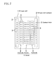
(Variation 3 of Example 1)
FIG. 7 shows Variation 3 of Example 1.
In Variation 3 of Example 1, the well contact 2 having the shape of a rectangular frame has a plurality of contact holes 3 only in portions which face the longer sides of the diffusion layers 4 constituting the cathode. Thus, as seen from FIG. 5 and FIG. 6, the upper and lower sides of the rectangular well contact 2 do not have the contact holes 3.
In view of this, according to Variation 3 of Example 1, as illustrated in FIG. 7, the upper and lower sides of the rectangular well contact 2 which do not have the contact holes 3 are removed, such that the well contact 2 is formed only by the left and right side portions which face the longer sides of the diffusion layers 4 constituting the cathode. In Variation 3 of Example 1, the same functions and effects as those of Variation 2 of Example 1 are achieved.
EXAMPLE 2
Next, a semiconductor integrated circuit according to Example 2 of the present invention is described with reference to FIG. 8.
As shown in FIG. 8, the structure of Example 2 is the same as the structure of FIG. 1 in that a P-type diffusion layer 5 which constitutes the anode of a diode D is provided at the center, while two diffusion layers 4 which constitute the cathode are provided on the left and right sides of the anode, and that the diode D is surrounded by a well contact 2.
In Example 2, portions of the well contact 2 extending parallel to a direction in which the diffusion layer 5 constituting the anode and the two diffusion layers 4 constituting the cathode face one another, i.e., the shorter side portions of the well contact 2, has a greater separation from the diffusion layers 4 and 5 of the anode and cathode (separation tL) than portions of the rectangular well contact 2 extending perpendicular to the direction in which the diffusion layer 5 of the anode and the diffusion layers 4 of the cathode face one another, i.e., the longer side portions of the well contact 2.
The positioning pitch of the contact holes 3 formed in the rectangular well contact 2 is equal to that of the contact holes 3 formed in the diffusion layers 4 and 5 of the anode and cathode.
In Example 2, separation tL between the diffusion layers 4 and 5 of the anode and cathode and the shorter side portions of the well contact 2 is longer than separation tS between the diffusion layers 4 of the cathode and the longer side portions of the well contact 2 (tL>tS). With this structure, the resistance value between the diffusion layer 5 of the anode and the shorter side portions of the well contact 2 is large. Thus, the current flowing from the diffusion layer 5 of the anode to the shorter side portions of the well contact 2 is restricted, so that convergence of the current at contact holes 3 formed along the edges of the diffusion layer 5 of the anode which are in the vicinity of the well contact 2 is reduced. As a result, breakage and deterioration in reliability of the diode D can be effectively prevented.
In the above description, the diode D is formed by the diffusion layer 5 of the anode at the center and the two diffusion layers 4 of the cathode which are provided on the left and right sides of the diffusion layer 5, but the present invention is not limited to this arrangement. Various other diode configurations are employable. For example, as illustrated in the semiconductor integrated circuit shown in FIG. 9, the diode D may have three diffusion layers 5 of the anode and four diffusion layers 4 of the cathode such that the diffusion layers 5 of the anode are provided alternately between the four diffusion layers 4 of the cathode. This also applies to the following descriptions.
(Variation 1 of Example 2)
FIG. 10 shows Variation 1 of Example 2.
In Variation 1 of Example 2, separation tL between the shorter side portions of the well contact 2 and the diffusion layers 5 and 4 of the anode and cathode is longer than separation tS between the longer side portions of the well contact 2 and the diffusion layers 4 of the cathode as in Example 2. In addition, as in Example 1, the positioning pitch of the contact holes 3 formed in the well contact 2, “pc”, is greater than the maximum pitch of the contact holes 3 of the P-type diffusion layer 5 which constitutes the anode, i.e., the vertical positioning pitch “py” (pc>py) as shown in FIG. 10. Therefore, Variation 1 of Example 2 provides the functions and effects of Example 1 in addition to those of Example 2.
(Variation 2 of Example 2)
FIG. 11 shows Variation 2 of Example 2.
In Variation 2 of Example 2, separation tL between the shorter side portions of the well contact 2 and the diffusion layers 5 and 4 of the anode and cathode is longer than separation tS between the longer side portions of the well contact 2 and the diffusion layers 4 of the cathode as in Example 2. In addition, as in Variation 1 of Example 1, the shorter side portions of the N-type well contact 2 (i.e., portions of the N-type well contact 2 extending parallel to a direction in which the P-type diffusion layer 5 constituting the anode and the two diffusion layers 4 constituting the cathode face one another) do not have the contact holes 3 as shown in FIG. 11. It should be noted that, in FIG. 11, the positioning pitch of the contact holes 3 formed in the longer side portions of the well contact 2 is equal to the maximum pitch of the contact holes 3 of the P-type diffusion layer 5 which constitutes the anode (vertical positioning pitch).
Therefore, Variation 2 of Example 2 provides the functions and effects of Variation 1 of Example 1 in addition to those of Example 2.
(Variation 3 of Example 2)
FIG. 12 shows Variation 3 of Example 2.
In Variation 3 of Example 2, separation tL between the shorter side portions of the well contact 2 and the diffusion layers 5 and 4 of the anode and cathode is longer than separation tS between the longer side portions of the well contact 2 and the diffusion layers 4 of the cathode as in Example 2. In addition, as in Variation 2 of Example 1, the well contact 2 has a plurality of contact holes 3 only in portions which face the longer sides of the diffusion layers 4 constituting the cathode.
Therefore, Variation 3 of Example 2 provides the functions and effects of Variation 2 of Example 1 in addition to those of Example 2.
Although in Variation 3 of Example 2 the well contact 2 has the shape of a rectangular frame, the shorter side portions of the well contact 2 may be omitted as in FIG. 7 because the shorter side portions do not have the contact holes 3.
EXAMPLE 3
Next, a semiconductor integrated circuit according to Example 3 of the present invention is described with reference to FIG. 13.
As shown in FIG. 13, the structure of Example 3 is the same as the structure of FIG. 1 in that a P-type diffusion layer 5 which constitutes the anode of a diode D is provided at the center, while two N-type diffusion layers 4 which constitute the cathode are provided on the left and right sides of the diffusion layer 5 of the anode, and that the diode D is surrounded by a well contact 2.
In Example 3, the rectangular well contact 2 is not separate from but shares a diffusion layer with the two N-type diffusion layers 4 which constitute the cathode. With this structure, the potential of the two N-type diffusion layers 4 which constitute the cathode of the diode D is equal to the potential of the well contact 2.
In Example 3, separation tL between the shorter side portions of the well contact 2 and the diffusion layers 5 and 4 of the anode and cathode is longer as in the semiconductor integrated circuit of Example 2 shown in FIG. 8.
Therefore, in Example 3 shown in FIG. 13, the space between the longer sides of the well contact 2 and the diffusion layers 4 of the cathode can be reduced as seen from comparison with FIG. 8. Thus, Example 3 provides the effect of reducing the area of the protection device in addition to the functions and effects of Example 2.
(Variation 1 of Example 3)
FIG. 14 shows Variation 1 of Example 3.
In Variation 1 of Example 3, the longer side portions of the well contact 2 share a diffusion layer with the two N-type diffusion layers 4 constituting the cathode, and separation tL between the shorter side portions of the well contact 2 and the diffusion layers 5 and 4 of the anode and cathode is longer, as in Example 3 shown in FIG. 13. In addition, Variation 1 of Example 3 shown in FIG. 14 is the same as Example 1 of FIG. 1 in that the positioning pitch “pc” of the contact holes 3 formed in the well contact 2 is greater than the maximum pitch of the contact holes 3 in the P-type diffusion layer 5 which constitutes the anode, i.e., the vertical positioning pitch “py” (pc>py).
Therefore, Variation 1 of Example 3 provides the functions and effects of Example 1 in addition to those of Example 3.
(Variation 2 of Example 3)
FIG. 15 shows Variation 2 of Example 3.
Variation 2 of Example 3 is different from Variation 1 of Example 3 in the following aspects. In Variation 2 of Example 3, the positioning pitch of the contact holes 3 formed in the well contact 2 is equal to the positioning pitch of the contact holes 3 of the diffusion layers 4 which constitute the cathode along the longer sides of the diffusion layers 4 as shown in FIG. 15, although in Variation 1 of Example 3 the positioning pitch “pc” of the contact holes 3 formed in the well contact 2 is longer. In Variation 2 of Example 3, the shorter side portions of the well contact 2 do not have the contact holes 3 as shown in FIG. 4 of Variation 1 of Example 1.
Therefore, Variation 2 of Example 3 provides the functions and effects of Variation 1 of Example 1 in addition to those of Example 3.
(Variation 3 of Example 3)
FIG. 16 shows Variation 3 of Example 3.
The structure of Variation 3 of Example 3 is different from Variation 2 of Example 3 shown in FIG. 15 in that parts of the longer side portions of the well contact 2 which do not face the diffusion layers 4 constituting the cathode do not have the contact holes 3, and that the contact holes 3 are formed only in parts of the longer side portions of the well contact 2 which face the diffusion layers 4 constituting the cathode. The other features of the structure are the same as those of FIG. 15.
Therefore, Variation 3 of Example 3 provides the functions and effects of Variation 2 of Example 1 in addition to those of Example 3.
(Variation 4 of Example 3)
FIG. 17 shows Variation 4 of Example 3.
The structure of Variation 4 of Example 3 is different from Variation 3 of Example 3 shown in FIG. 16 in that the longer side portions of the well contact 2 do not have the contact holes 3. As a result, the number of contact holes 3 of the diffusion layer 5 which constitutes the anode is equal to the total number of contact holes 3 of the two diffusion layers 4 which constitute the cathode. The other features of the structure are the same as those of FIG. 16.
Thus, in Variation 4 of Example 3, in addition to the functions and effects of Variation 3 of Example 3, the number of contact holes 3 of the diffusion layer 5 which constitutes the anode is equal to the number of contact holes 3 of the diffusion layers 4 which constitute the cathode. Accordingly, the current density in the anode is equal to the current density in the cathode. Therefore, the reliability of the diode D is improved.
EXAMPLE 4
Next, a semiconductor integrated circuit according to Example 4 of the present invention is described with reference to FIG. 18.
In Example 4, as shown in FIG. 18, a P-type diffusion layer 5 which constitutes the anode of a diode D is provided at the center, while two N-type diffusion layers 4 which constitute the cathode are provided on the left and right sides of the diffusion layer 5 of the anode. Example 4 does not have a rectangular well contact surrounding the diode D. Instead, the two N-type diffusion layers 4 which constitute the cathode substitute for the well contact.
Since in Example 4 an exclusive well contact is not provided, all of currents from the diffusion layer 5 which constitutes the anode infallibly flow into the diffusion layers 4 which constitute the cathode. Namely, the current flow from the diffusion layer 5 of the anode to the well contact, which would occur in the conventionally-proposed example, does not occur. Thus, convergence of the current at contact holes 3 of the diffusion layer 5 of the anode is infallibly reduced. Therefore, breakage and deterioration in reliability of the diode D can be prevented. Further, in Example 4, the area of the semiconductor integrated circuit is effectively reduced by omission of the exclusive well contact.
(Variation 1 of Example 4)
FIG. 19 shows Variation 1 of Example 4.
In Variation 1 of Example 4, as shown in FIG. 19, the semiconductor integrated circuit does not have an exclusive well contact. Instead, the two N-type diffusion layers 4 which constitute the cathode substitute for the well contact. Further, the number of contact holes 3 of the diffusion layer 5 which constitutes the anode is equal to the total number of contact holes 3 of the diffusion layers 4 which constitute the cathode.
Thus, in Variation 1 of Example 4, in addition to the functions and effects of Example 4, the largeness of the current flowing out of the anode is equal to the largeness of the current flowing into the cathode. Accordingly, convergence of the current at the contact holes 3 of the diffusion layer 5 which constitutes the anode is avoided. Therefore, breakage and deterioration in reliability of the diode D can be prevented.

Claims (16)

1. A semiconductor integrated circuit, comprising:
a diode including a first polarity-type diffusion layer which constitutes an anode of the diode and a second polarity-type diffusion layer which faces the first polarity-type diffusion layer and which constitutes a cathode of the diode; and
a second polarity-type substrate or well contact which shares a diffusion layer with the second polarity-type diffusion layer constituting the cathode of the diode and which surrounds four sides of the diode, wherein:
each of the first polarity-type diffusion layer and second polarity-type diffusion layer of the diode and the substrate or well contact has a plurality of contact holes for electrical connection with an external device,
a portion of the substrate or well contact extending parallel to a direction in which the first polarity-type diffusion layer and the second polarity-type diffusion layer face each other has a greater separation from the first polarity-type diffusion layer or second polarity-type diffusion layer of the diode than a portion of the substrate or well contact extending perpendicular to the facing direction of the diffusion layers, and
the substrate or well contact has the plurality of contact holes only in a portion extending perpendicular to the direction in which the first polarity-type diffusion layer and the second polarity-type diffusion layer face each other.
2. The semiconductor integrated circuit of claim 1, wherein the number of contact holes formed in the first polarity-type diffusion layer which constitutes the anode of the diode is equal to the number of contact holes formed in the second polarity-type diffusion layer which shares a diffusion layer with the second polarity-type substrate or well contact and which constitutes the cathode of the diode.
3. The semiconductor integrated circuit of claim 1, wherein the first polarity-type diffusion layer which constitutes the anode of the diode and the second polarity-type diffusion layer which constitutes the cathode of the diode have the shape of a rectangular strip.
4. A system LSI, comprising:
a digital circuit and an analog circuit which operate on separate power supplies; and
a single unit of protection device formed by two semiconductor integrated circuits of claim 1 and provided between the digital circuit and the analog circuit for allowing electrostatic discharge from the digital circuit to the analog circuit and electrostatic discharge from the analog circuit to the digital circuit.
5. A semiconductor integrated circuit, comprising:
a first polarity-type diffusion layer having a first polarity-type diode region; and
a second polarity-type diffusion layer having a second polarity-type diode region and a contact region, wherein:
the first polarity-type diode region and the second polarity-type diode region constitute a diode,
the second polarity-type diode region is disposed next to the first polarity-type diode region in a first direction in a plan view,
the contact region surrounds, in a plan view, four sides of the diode including the first polarity-type diode region and the second polarity-type diode region,
the contact region has a first contact region facing a side of the first polarity-type diode region, the side extending along the first direction, and a second contact region extending along a second direction perpendicular to the first direction in a plan view,
each of the first polarity-type diode region and the second polarity-type diode region has a plurality of contact holes for electrical connection with an external device, and
the second contact region extending along the second direction of the contact region has a plurality of contact holes and the first contact region facing the side of the first polarity-type diode region has no contact hole, in a plan view.
6. The semiconductor integrated circuit according to claim 5, wherein the first polarity-type diffusion layer constitutes an anode of the diode and has a rectangular stripe.
7. The semiconductor integrated circuit according to claim 5, wherein the second polarity-type diffusion layer constitutes a cathode of the diode and is provided on both left and right sides of the first polarity-type diffusion layer which constitute an anode of the diode in a plan view.
8. The semiconductor integrated circuit according to claim 7, the second polarity-type diffusion layer disposed on the left side of the first polarity-type diffusion layer and the second polarity-type diffusion layer disposed on the right side of the first polarity-type diffusion layer are connected via the first contact region.
9. The semiconductor integrated circuit of claim 5, wherein the second polarity-type diffusion layer includes two second polarity-type diffusion layers which sandwich the first polarity-type diffusion layer in a plan view.
10. The semiconductor integrated circuit according to claim 9, the two second polarity-type diffusion layers are connected via the first contact region.
11. A system LSI, comprising:
a digital circuit and an analog circuit which operate on separate power supplies; and
a single unit of protection device formed by two semiconductor integrated circuits, each according to claim 5, and provided between the digital circuit and the analog circuit for allowing electrostatic discharge from the digital circuit to the analog circuit and electrostatic charge from the analog circuit to the digital circuit.
12. A semiconductor integrated circuit, comprising:
a first polarity-type diffusion region having a plurality of first contact holes; and
two second polarity-type diffusion regions having a plurality of second contact holes, wherein:
the two second polarity-type diffusion regions sandwich the first polarity-type diffusion region, in a plan view, in a first direction,
a length of the second polarity-type diffusion regions in a second direction perpendicular to the first direction is longer than a length of the first polarity-type diffusion region in the second direction,
the two second polarity-type diffusion regions are connected by a connection region having no contact hole.
13. The semiconductor integrated circuit according to claim 12, wherein the connection region has no contact hole at a portion facing the first polarity-type diffusion region.
14. The semiconductor integrated circuit according to claim 12, wherein the first polarity-type diffusion region constitutes an anode of a diode and has a rectangular stripe.
15. The semiconductor integrated circuit according to claim 14, wherein the second polarity-type diffusion regions constitute an cathode of the diode.
16. A system LSI, comprising:
a digital circuit and an analog circuit which operate on separate power supplies; and
a single unit of protection device formed by two semiconductor integrated circuits, each according to claim 12, and provided between the digital circuit and the analog circuit for allowing electrostatic discharge from the digital circuit to the analog circuit and electrostatic charge from the analog circuit to the digital circuit.
US12/883,546 2006-04-27 2010-09-16 Semiconductor integrated circuit and system LSI including the same Active US8102024B2 (en)

Priority Applications (1)

Application Number Priority Date Filing Date Title
US12/883,546 US8102024B2 (en) 2006-04-27 2010-09-16 Semiconductor integrated circuit and system LSI including the same

Applications Claiming Priority (4)

Application Number Priority Date Filing Date Title
JP2006124110A JP4993941B2 (en) 2006-04-27 2006-04-27 Semiconductor integrated circuit and system LSI having the same
JP2006-124110 2006-04-27
US11/783,133 US7821096B2 (en) 2006-04-27 2007-04-06 Semiconductor integrated circuit and system LSI including the same
US12/883,546 US8102024B2 (en) 2006-04-27 2010-09-16 Semiconductor integrated circuit and system LSI including the same

Related Parent Applications (1)

Application Number Title Priority Date Filing Date
US11/783,133 Division US7821096B2 (en) 2006-04-27 2007-04-06 Semiconductor integrated circuit and system LSI including the same

Publications (2)

Publication Number Publication Date
US20110001218A1 US20110001218A1 (en) 2011-01-06
US8102024B2 true US8102024B2 (en) 2012-01-24

Family

ID=38647555

Family Applications (2)

Application Number Title Priority Date Filing Date
US11/783,133 Active 2028-09-03 US7821096B2 (en) 2006-04-27 2007-04-06 Semiconductor integrated circuit and system LSI including the same
US12/883,546 Active US8102024B2 (en) 2006-04-27 2010-09-16 Semiconductor integrated circuit and system LSI including the same

Family Applications Before (1)

Application Number Title Priority Date Filing Date
US11/783,133 Active 2028-09-03 US7821096B2 (en) 2006-04-27 2007-04-06 Semiconductor integrated circuit and system LSI including the same

Country Status (3)

Country Link
US (2) US7821096B2 (en)
JP (1) JP4993941B2 (en)
CN (2) CN102184919B (en)

Cited By (1)

* Cited by examiner, † Cited by third party
Publication number Priority date Publication date Assignee Title
US20140191368A1 (en) * 2011-09-16 2014-07-10 Panasonic Corporation Semiconductor integrated circuit device

Families Citing this family (8)

* Cited by examiner, † Cited by third party
Publication number Priority date Publication date Assignee Title
JP4993941B2 (en) * 2006-04-27 2012-08-08 パナソニック株式会社 Semiconductor integrated circuit and system LSI having the same
KR20100052948A (en) * 2008-11-11 2010-05-20 삼성전자주식회사 Composition for radical polymerization and method for fabricating a pattern using the composition
JP2010129893A (en) * 2008-11-28 2010-06-10 Sony Corp Semiconductor integrated circuit
KR20130008279A (en) * 2011-07-12 2013-01-22 삼성전자주식회사 Power semiconductor device
JP5678341B2 (en) * 2013-08-23 2015-03-04 株式会社レーザーシステム Schottky barrier diode, method for manufacturing Schottky barrier diode, power transmission system, and wireless connector for power line
JP6311468B2 (en) * 2014-06-12 2018-04-18 株式会社ソシオネクスト Semiconductor device and integrated circuit
JP6287958B2 (en) * 2015-05-27 2018-03-07 トヨタ自動車株式会社 Semiconductor device
CN105609500B (en) * 2016-01-28 2018-10-12 嘉兴爱禾电子有限公司 A kind of copolar integrated diode

Citations (25)

* Cited by examiner, † Cited by third party
Publication number Priority date Publication date Assignee Title
JPH03234063A (en) 1990-02-09 1991-10-18 Sharp Corp Semiconductor integrated circuit
US5066999A (en) * 1989-10-23 1991-11-19 Micron Technology, Inc. Resistor under wirebond pad
US5196692A (en) 1991-02-01 1993-03-23 Fujitsu Limited Photoelectric transducer switchable to a high-resolution or high-sensitivity mode
US5497023A (en) 1985-09-25 1996-03-05 Hitachi, Ltd. Semiconductor memory device having separately biased wells for isolation
US5565698A (en) * 1994-07-04 1996-10-15 Deutsche Itt Industries Gmbh IC protection structure having n-channel MOSFET with n-type resistor region
US5682047A (en) 1995-06-07 1997-10-28 Lsi Logic Corporation Input-output (I/O) structure with capacitively triggered thyristor for electrostatic discharge (ESD) protection
US5686750A (en) 1991-09-27 1997-11-11 Koshiba & Partners Power semiconductor device having improved reverse recovery voltage
US5744854A (en) * 1995-08-10 1998-04-28 Nippondenso Co., Ltd. Surge protective device having a surface collector region directly shorted to a base region
US5760428A (en) 1996-01-25 1998-06-02 Lsi Logic Corporation Variable width low profile gate array input/output architecture
US5767552A (en) * 1995-11-30 1998-06-16 Micron Technology, Inc. Structure for ESD protection in semiconductor chips
US5796147A (en) * 1993-08-09 1998-08-18 Kabushiki Kaisha Toshiba Semiconductor device having a plurality of circuits driven by different power sources and formed on the same substrate
JPH11135734A (en) 1997-10-31 1999-05-21 Seiko Epson Corp Semiconductor device
US5910675A (en) 1995-12-14 1999-06-08 Nec Corporation Semiconductor device and method of making the same
US5955764A (en) 1994-10-06 1999-09-21 Fujitsu Limited MOS LSI with projection structure
US6043542A (en) 1997-01-29 2000-03-28 Micron Technology, Inc. Method and integrated circuit structure for preventing latch-up in CMOS integrated circuit devices
US6118154A (en) 1996-03-29 2000-09-12 Mitsubishi Denki Kabushiki Kaisha Input/output protection circuit having an SOI structure
US20020153571A1 (en) * 2001-03-16 2002-10-24 Mergens Markus Paul Josef Electrostatic discharge protection structures having high holding current for latch-up immunity
US20020190279A1 (en) * 2001-04-02 2002-12-19 Matsushita Electric Industrial Co., Ltd. Analog MOS semiconductor device, manufacturing method therefor, manufacturing program therefor, and program device therefor
US6587320B1 (en) * 2000-01-04 2003-07-01 Sarnoff Corporation Apparatus for current ballasting ESD sensitive devices
US20040012066A1 (en) * 2001-01-11 2004-01-22 Josef Dietl Schottky diode
US20040150053A1 (en) * 1998-11-10 2004-08-05 Hitachi, Ltd. Semiconductor integrated circuit device with connections formed using a conductor embedded in a contact hole
US20060226499A1 (en) * 2005-03-31 2006-10-12 Akira Shimizu Semiconductor device incorporating protective diode with stable ESD protection capabilities
US7335954B2 (en) * 2005-04-20 2008-02-26 Delphi Technolgoies, Inc. Electrostatic discharge protection device
US7821096B2 (en) * 2006-04-27 2010-10-26 Panasonic Corporation Semiconductor integrated circuit and system LSI including the same
US7888739B2 (en) * 2005-02-07 2011-02-15 Samsung Electronics Co., Ltd. Electrostatic discharge circuit and method of dissipating an electrostatic current

Family Cites Families (12)

* Cited by examiner, † Cited by third party
Publication number Priority date Publication date Assignee Title
JPH0453169A (en) * 1990-06-18 1992-02-20 Nec Corp Semiconductor protective device
US5440162A (en) * 1994-07-26 1995-08-08 Rockwell International Corporation ESD protection for submicron CMOS circuits
JP3319920B2 (en) * 1995-10-12 2002-09-03 株式会社ユニシアジェックス Engine Valve Actuator
KR100258436B1 (en) * 1996-10-11 2000-06-01 김덕중 Complementary bipolar transistor and method for manufacturing the same
KR100205609B1 (en) * 1997-01-06 1999-07-01 윤종용 An electrostatic protection device
JPH11204732A (en) * 1998-01-14 1999-07-30 Toshiba Microelectronics Corp Semiconductor protecting device
KR100268453B1 (en) * 1998-03-30 2000-11-01 윤종용 Semiconductor device and its manufacturing method
FR2781786B1 (en) * 1998-07-29 2000-10-13 Stein Heurtey DEVICE FOR CONDUCTING GLASS MELTING AND / OR REFINING OVENS
KR100495069B1 (en) * 2002-11-29 2005-06-14 엘지전자 주식회사 A tub for drum washing machine
JP4708716B2 (en) * 2003-02-27 2011-06-22 ルネサスエレクトロニクス株式会社 Semiconductor integrated circuit device and method for designing semiconductor integrated circuit device
JP3773506B2 (en) * 2003-07-24 2006-05-10 松下電器産業株式会社 Semiconductor integrated circuit device
JP4323392B2 (en) * 2004-07-14 2009-09-02 Okiセミコンダクタ株式会社 Semiconductor integrated circuit

Patent Citations (30)

* Cited by examiner, † Cited by third party
Publication number Priority date Publication date Assignee Title
US5497023A (en) 1985-09-25 1996-03-05 Hitachi, Ltd. Semiconductor memory device having separately biased wells for isolation
US5066999A (en) * 1989-10-23 1991-11-19 Micron Technology, Inc. Resistor under wirebond pad
JP2598147B2 (en) 1990-02-09 1997-04-09 シャープ株式会社 Semiconductor integrated circuit
JPH03234063A (en) 1990-02-09 1991-10-18 Sharp Corp Semiconductor integrated circuit
US5196692A (en) 1991-02-01 1993-03-23 Fujitsu Limited Photoelectric transducer switchable to a high-resolution or high-sensitivity mode
US5686750A (en) 1991-09-27 1997-11-11 Koshiba & Partners Power semiconductor device having improved reverse recovery voltage
US5796147A (en) * 1993-08-09 1998-08-18 Kabushiki Kaisha Toshiba Semiconductor device having a plurality of circuits driven by different power sources and formed on the same substrate
US5565698A (en) * 1994-07-04 1996-10-15 Deutsche Itt Industries Gmbh IC protection structure having n-channel MOSFET with n-type resistor region
US5955764A (en) 1994-10-06 1999-09-21 Fujitsu Limited MOS LSI with projection structure
US5682047A (en) 1995-06-07 1997-10-28 Lsi Logic Corporation Input-output (I/O) structure with capacitively triggered thyristor for electrostatic discharge (ESD) protection
US5744854A (en) * 1995-08-10 1998-04-28 Nippondenso Co., Ltd. Surge protective device having a surface collector region directly shorted to a base region
US6586290B1 (en) * 1995-11-30 2003-07-01 Micron Technology, Inc. Structure for ESD protection in semiconductor chips
US5767552A (en) * 1995-11-30 1998-06-16 Micron Technology, Inc. Structure for ESD protection in semiconductor chips
US5910675A (en) 1995-12-14 1999-06-08 Nec Corporation Semiconductor device and method of making the same
US5760428A (en) 1996-01-25 1998-06-02 Lsi Logic Corporation Variable width low profile gate array input/output architecture
US6118154A (en) 1996-03-29 2000-09-12 Mitsubishi Denki Kabushiki Kaisha Input/output protection circuit having an SOI structure
US6043542A (en) 1997-01-29 2000-03-28 Micron Technology, Inc. Method and integrated circuit structure for preventing latch-up in CMOS integrated circuit devices
JPH11135734A (en) 1997-10-31 1999-05-21 Seiko Epson Corp Semiconductor device
US20040150053A1 (en) * 1998-11-10 2004-08-05 Hitachi, Ltd. Semiconductor integrated circuit device with connections formed using a conductor embedded in a contact hole
US6587320B1 (en) * 2000-01-04 2003-07-01 Sarnoff Corporation Apparatus for current ballasting ESD sensitive devices
US20040012066A1 (en) * 2001-01-11 2004-01-22 Josef Dietl Schottky diode
US6885077B2 (en) * 2001-01-11 2005-04-26 Infineon Technologies Ag Schottky diode
US20020153571A1 (en) * 2001-03-16 2002-10-24 Mergens Markus Paul Josef Electrostatic discharge protection structures having high holding current for latch-up immunity
US20040164356A1 (en) * 2001-03-16 2004-08-26 Sarnoff Corporation Electrostatic discharge protection structures having high holding current for latch-up immunity
US7064393B2 (en) 2001-03-16 2006-06-20 Sarnoff Corporation Electrostatic discharge protection structures having high holding current for latch-up immunity
US20020190279A1 (en) * 2001-04-02 2002-12-19 Matsushita Electric Industrial Co., Ltd. Analog MOS semiconductor device, manufacturing method therefor, manufacturing program therefor, and program device therefor
US7888739B2 (en) * 2005-02-07 2011-02-15 Samsung Electronics Co., Ltd. Electrostatic discharge circuit and method of dissipating an electrostatic current
US20060226499A1 (en) * 2005-03-31 2006-10-12 Akira Shimizu Semiconductor device incorporating protective diode with stable ESD protection capabilities
US7335954B2 (en) * 2005-04-20 2008-02-26 Delphi Technolgoies, Inc. Electrostatic discharge protection device
US7821096B2 (en) * 2006-04-27 2010-10-26 Panasonic Corporation Semiconductor integrated circuit and system LSI including the same

Non-Patent Citations (1)

* Cited by examiner, † Cited by third party
Title
Chinese Office Action, w/ English translation thereof, issued in Chinese Patent Application No. CN 200710091778.8 dated Dec. 11, 2009.

Cited By (9)

* Cited by examiner, † Cited by third party
Publication number Priority date Publication date Assignee Title
US20140191368A1 (en) * 2011-09-16 2014-07-10 Panasonic Corporation Semiconductor integrated circuit device
US8994111B2 (en) * 2011-09-16 2015-03-31 Panasonic Corporation Semiconductor integrated circuit device
US9224725B2 (en) 2011-09-16 2015-12-29 Socionext Inc. Semiconductor integrated circuit device
US9385113B2 (en) 2011-09-16 2016-07-05 Socionext Inc. Semiconductor integrated circuit device
US9653452B2 (en) 2011-09-16 2017-05-16 Socionext Inc. Semiconductor integrated circuit device having an ESD protection circuit
US9871033B2 (en) 2011-09-16 2018-01-16 Socionext Inc. Semiconductor integrated circuit device
US10096593B2 (en) 2011-09-16 2018-10-09 Socionext Inc. Semiconductor integrated circuit device having an ESD protection circuit
US10446540B2 (en) 2011-09-16 2019-10-15 Socionext Inc. Semiconductor integrated circuit device
US10658355B2 (en) 2011-09-16 2020-05-19 Socionext Inc. Semiconductor integrated circuit device

Also Published As

Publication number Publication date
JP2007299790A (en) 2007-11-15
CN102184919A (en) 2011-09-14
US7821096B2 (en) 2010-10-26
US20110001218A1 (en) 2011-01-06
CN101064306B (en) 2011-06-29
JP4993941B2 (en) 2012-08-08
CN102184919B (en) 2013-01-16
US20070252231A1 (en) 2007-11-01
CN101064306A (en) 2007-10-31

Similar Documents

Publication Publication Date Title
US8102024B2 (en) Semiconductor integrated circuit and system LSI including the same
US7280329B2 (en) Integrated circuit device having input/output electrostatic discharge protection cell equipped with electrostatic discharge protection element and power clamp
JP5322441B2 (en) Layout structure of semiconductor device
US7989846B2 (en) Semiconductor device with three-dimensional field effect transistor structure
US8008723B2 (en) Semiconductor device including a plurality of diffusion layers and diffusion resistance layer
US20170243888A1 (en) Layout structure for semiconductor integrated circuit
US20170213819A1 (en) Semiconductor integrated circuit device
US20080073721A1 (en) Semiconductor integrated circuit device
CN111033720B (en) Semiconductor integrated circuit device having a plurality of semiconductor chips
US20030157811A1 (en) Semiconductor device
US8072033B2 (en) Semiconductor device having elongated electrostatic protection element along long side of semiconductor chip
JP4312696B2 (en) Semiconductor integrated device
US6730985B2 (en) Semiconductor integrated circuit device
US7847324B2 (en) MOS transistor and semiconductor integrated circuit
JP7231427B2 (en) semiconductor equipment
WO2023167083A1 (en) Semiconductor integrated circuit device
JP2008021852A (en) Semiconductor device
US20080074169A1 (en) Semiconductor integrated circuit device
KR100638887B1 (en) Electrostatic discharge device for bonding pad
KR20030093115A (en) Semiconductor integrated circuit device
JPWO2013018589A1 (en) Semiconductor integrated circuit device
JP4555578B2 (en) Integrated circuit
JP2004311670A (en) Semiconductor device

Legal Events

Date Code Title Description
FEPP Fee payment procedure

Free format text: PAYOR NUMBER ASSIGNED (ORIGINAL EVENT CODE: ASPN); ENTITY STATUS OF PATENT OWNER: LARGE ENTITY

STCF Information on status: patent grant

Free format text: PATENTED CASE

AS Assignment

Owner name: SOCIONEXT INC., JAPAN

Free format text: ASSIGNMENT OF ASSIGNORS INTEREST;ASSIGNOR:PANASONIC CORPORATION;REEL/FRAME:035294/0942

Effective date: 20150302

FPAY Fee payment

Year of fee payment: 4

MAFP Maintenance fee payment

Free format text: PAYMENT OF MAINTENANCE FEE, 8TH YEAR, LARGE ENTITY (ORIGINAL EVENT CODE: M1552); ENTITY STATUS OF PATENT OWNER: LARGE ENTITY

Year of fee payment: 8

MAFP Maintenance fee payment

Free format text: PAYMENT OF MAINTENANCE FEE, 12TH YEAR, LARGE ENTITY (ORIGINAL EVENT CODE: M1553); ENTITY STATUS OF PATENT OWNER: LARGE ENTITY

Year of fee payment: 12