US8102027B2 - IC package sacrificial structures for crack propagation confinement - Google Patents
IC package sacrificial structures for crack propagation confinement Download PDFInfo
- Publication number
- US8102027B2 US8102027B2 US12/073,450 US7345008A US8102027B2 US 8102027 B2 US8102027 B2 US 8102027B2 US 7345008 A US7345008 A US 7345008A US 8102027 B2 US8102027 B2 US 8102027B2
- Authority
- US
- United States
- Prior art keywords
- unit
- preventive structure
- vias
- functional area
- preventive
- Prior art date
- Legal status (The legal status is an assumption and is not a legal conclusion. Google has not performed a legal analysis and makes no representation as to the accuracy of the status listed.)
- Active, expires
Links
Images


Classifications
-
- H—ELECTRICITY
- H01—ELECTRIC ELEMENTS
- H01L—SEMICONDUCTOR DEVICES NOT COVERED BY CLASS H10
- H01L23/00—Details of semiconductor or other solid state devices
- H01L23/28—Encapsulations, e.g. encapsulating layers, coatings, e.g. for protection
-
- H—ELECTRICITY
- H01—ELECTRIC ELEMENTS
- H01L—SEMICONDUCTOR DEVICES NOT COVERED BY CLASS H10
- H01L21/00—Processes or apparatus adapted for the manufacture or treatment of semiconductor or solid state devices or of parts thereof
- H01L21/70—Manufacture or treatment of devices consisting of a plurality of solid state components formed in or on a common substrate or of parts thereof; Manufacture of integrated circuit devices or of parts thereof
- H01L21/77—Manufacture or treatment of devices consisting of a plurality of solid state components or integrated circuits formed in, or on, a common substrate
- H01L21/78—Manufacture or treatment of devices consisting of a plurality of solid state components or integrated circuits formed in, or on, a common substrate with subsequent division of the substrate into plural individual devices
-
- H—ELECTRICITY
- H01—ELECTRIC ELEMENTS
- H01L—SEMICONDUCTOR DEVICES NOT COVERED BY CLASS H10
- H01L23/00—Details of semiconductor or other solid state devices
- H01L23/48—Arrangements for conducting electric current to or from the solid state body in operation, e.g. leads, terminal arrangements ; Selection of materials therefor
-
- H—ELECTRICITY
- H01—ELECTRIC ELEMENTS
- H01L—SEMICONDUCTOR DEVICES NOT COVERED BY CLASS H10
- H01L23/00—Details of semiconductor or other solid state devices
- H01L23/562—Protection against mechanical damage
-
- H—ELECTRICITY
- H01—ELECTRIC ELEMENTS
- H01L—SEMICONDUCTOR DEVICES NOT COVERED BY CLASS H10
- H01L23/00—Details of semiconductor or other solid state devices
- H01L23/58—Structural electrical arrangements for semiconductor devices not otherwise provided for, e.g. in combination with batteries
- H01L23/585—Structural electrical arrangements for semiconductor devices not otherwise provided for, e.g. in combination with batteries comprising conductive layers or plates or strips or rods or rings
-
- H—ELECTRICITY
- H05—ELECTRIC TECHNIQUES NOT OTHERWISE PROVIDED FOR
- H05K—PRINTED CIRCUITS; CASINGS OR CONSTRUCTIONAL DETAILS OF ELECTRIC APPARATUS; MANUFACTURE OF ASSEMBLAGES OF ELECTRICAL COMPONENTS
- H05K3/00—Apparatus or processes for manufacturing printed circuits
- H05K3/0011—Working of insulating substrates or insulating layers
- H05K3/0044—Mechanical working of the substrate, e.g. drilling or punching
- H05K3/0052—Depaneling, i.e. dividing a panel into circuit boards; Working of the edges of circuit boards
-
- H—ELECTRICITY
- H01—ELECTRIC ELEMENTS
- H01L—SEMICONDUCTOR DEVICES NOT COVERED BY CLASS H10
- H01L2924/00—Indexing scheme for arrangements or methods for connecting or disconnecting semiconductor or solid-state bodies as covered by H01L24/00
- H01L2924/0001—Technical content checked by a classifier
- H01L2924/0002—Not covered by any one of groups H01L24/00, H01L24/00 and H01L2224/00
-
- H—ELECTRICITY
- H05—ELECTRIC TECHNIQUES NOT OTHERWISE PROVIDED FOR
- H05K—PRINTED CIRCUITS; CASINGS OR CONSTRUCTIONAL DETAILS OF ELECTRIC APPARATUS; MANUFACTURE OF ASSEMBLAGES OF ELECTRICAL COMPONENTS
- H05K2201/00—Indexing scheme relating to printed circuits covered by H05K1/00
- H05K2201/09—Shape and layout
- H05K2201/09009—Substrate related
- H05K2201/09063—Holes or slots in insulating substrate not used for electrical connections
-
- H—ELECTRICITY
- H05—ELECTRIC TECHNIQUES NOT OTHERWISE PROVIDED FOR
- H05K—PRINTED CIRCUITS; CASINGS OR CONSTRUCTIONAL DETAILS OF ELECTRIC APPARATUS; MANUFACTURE OF ASSEMBLAGES OF ELECTRICAL COMPONENTS
- H05K2201/00—Indexing scheme relating to printed circuits covered by H05K1/00
- H05K2201/09—Shape and layout
- H05K2201/09209—Shape and layout details of conductors
- H05K2201/09654—Shape and layout details of conductors covering at least two types of conductors provided for in H05K2201/09218 - H05K2201/095
- H05K2201/09681—Mesh conductors, e.g. as a ground plane
-
- H—ELECTRICITY
- H05—ELECTRIC TECHNIQUES NOT OTHERWISE PROVIDED FOR
- H05K—PRINTED CIRCUITS; CASINGS OR CONSTRUCTIONAL DETAILS OF ELECTRIC APPARATUS; MANUFACTURE OF ASSEMBLAGES OF ELECTRICAL COMPONENTS
- H05K2201/00—Indexing scheme relating to printed circuits covered by H05K1/00
- H05K2201/09—Shape and layout
- H05K2201/09209—Shape and layout details of conductors
- H05K2201/09654—Shape and layout details of conductors covering at least two types of conductors provided for in H05K2201/09218 - H05K2201/095
- H05K2201/09781—Dummy conductors, i.e. not used for normal transport of current; Dummy electrodes of components
Definitions
- Unit 102 a may be singulated in a variety of ways.
- methods for unit singulation may include sawing, punching, abrasive particle cutting, and focused laser beam ablation cutting. All of the above mentioned methods involve stress being applied to unit 102 a and/or adjacent units 102 b and 102 c .
- stress from a singulation process is present along boundaries 104 and 106 .
- unit 102 a may be singulated by sawing along boundaries 104 and 106 or applying a force on the top of unit 102 a in a punching action.
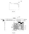
- Slots 304 generally have a larger width than slot 306 because slot 306 is located along an edge portion of strip 300 (i.e., does not border any other unit) in which space is limited. In alternate embodiments, slot 306 may have a width substantially similar to or larger than slots 304 .
- functional area 504 includes a via.
- vias of the plurality of vias 510 may be substantially similar, in terms of composition, size, etc., to the via of functional area 504 .
- vias of plurality of vias 510 may be included in the layout of substrate 500 and may be and fabricated in the same process in which features of functional area 504 are fabricated.
Abstract
Description
Claims (32)
Priority Applications (6)
| Application Number | Priority Date | Filing Date | Title |
|---|---|---|---|
| US12/073,450 US8102027B2 (en) | 2007-08-21 | 2008-03-05 | IC package sacrificial structures for crack propagation confinement |
| EP08014445A EP2028691A3 (en) | 2007-08-21 | 2008-08-13 | Sacrificial structures for crack propagation confinement in a substrate comprising a plurality of ICs |
| KR1020080081956A KR101005875B1 (en) | 2007-08-21 | 2008-08-21 | Ic package sacrificial structures for crack propagation confinement |
| CN2008102136903A CN101373743B (en) | 2007-08-21 | 2008-08-21 | Unit in unit set and manufacturing method thereof |
| TW097131899A TWI412113B (en) | 2007-08-21 | 2008-08-21 | Ic package sacrificial structures for crack propagation confinement |
| CN2011100375371A CN102194799A (en) | 2007-08-21 | 2008-08-21 | Unit in collection of units and its manufacture method |
Applications Claiming Priority (2)
| Application Number | Priority Date | Filing Date | Title |
|---|---|---|---|
| US93560607P | 2007-08-21 | 2007-08-21 | |
| US12/073,450 US8102027B2 (en) | 2007-08-21 | 2008-03-05 | IC package sacrificial structures for crack propagation confinement |
Publications (2)
| Publication Number | Publication Date |
|---|---|
| US20090051010A1 US20090051010A1 (en) | 2009-02-26 |
| US8102027B2 true US8102027B2 (en) | 2012-01-24 |
Family
ID=40090208
Family Applications (1)
| Application Number | Title | Priority Date | Filing Date |
|---|---|---|---|
| US12/073,450 Active 2030-03-13 US8102027B2 (en) | 2007-08-21 | 2008-03-05 | IC package sacrificial structures for crack propagation confinement |
Country Status (5)
| Country | Link |
|---|---|
| US (1) | US8102027B2 (en) |
| EP (1) | EP2028691A3 (en) |
| KR (1) | KR101005875B1 (en) |
| CN (2) | CN102194799A (en) |
| TW (1) | TWI412113B (en) |
Cited By (1)
| Publication number | Priority date | Publication date | Assignee | Title |
|---|---|---|---|---|
| US11387213B2 (en) * | 2020-06-05 | 2022-07-12 | Advanced Semiconductor Engineering, Inc. | Method for manufacturing a semiconductor package |
Families Citing this family (4)
| Publication number | Priority date | Publication date | Assignee | Title |
|---|---|---|---|---|
| KR101984736B1 (en) * | 2012-10-09 | 2019-06-03 | 삼성디스플레이 주식회사 | Array substrate for flexible display device |
| US9761774B2 (en) * | 2014-12-16 | 2017-09-12 | Epistar Corporation | Light-emitting element with protective cushioning |
| FR3058830B1 (en) * | 2016-11-14 | 2018-11-30 | Commissariat A L'energie Atomique Et Aux Energies Alternatives | PROCESS FOR THE COLLECTIVE PRODUCTION OF A PLURALITY OF OPTOELECTRONIC CHIPS |
| US11222867B1 (en) * | 2020-07-09 | 2022-01-11 | Taiwan Semiconductor Manufacturing Company, Ltd. | Package and manufacturing method thereof |
Citations (30)
| Publication number | Priority date | Publication date | Assignee | Title |
|---|---|---|---|---|
| US4610079A (en) | 1980-01-22 | 1986-09-09 | Tokyo Shibaura Denki Kabushiki Kaisha | Method of dicing a semiconductor wafer |
| JPH03171688A (en) | 1989-11-29 | 1991-07-25 | Seiko Epson Corp | Printed wiring board |
| JPH08172062A (en) | 1994-12-16 | 1996-07-02 | Oki Electric Ind Co Ltd | Semiconductor wafer and manufacture thereof |
| US5763936A (en) | 1995-04-27 | 1998-06-09 | Yamaha Corporation | Semiconductor chip capable of supressing cracks in insulating layer |
| US5834829A (en) | 1996-09-05 | 1998-11-10 | International Business Machines Corporation | Energy relieving crack stop |
| US6365958B1 (en) | 1998-02-06 | 2002-04-02 | Texas Instruments Incorporated | Sacrificial structures for arresting insulator cracks in semiconductor devices |
| US20030122220A1 (en) * | 1999-05-20 | 2003-07-03 | West Jeffrey A. | Scribe street seals in semiconductor devices and method of fabrication |
| KR20040104779A (en) | 2003-06-04 | 2004-12-13 | (주)이엠엘에스아이 | Semiconductor Device AND layout arrangement method therefor |
| US20050087878A1 (en) | 2003-10-23 | 2005-04-28 | Renesas Technology Corp. | Semiconductor device |
| US20060012012A1 (en) * | 2004-07-15 | 2006-01-19 | Ping-Wei Wang | Semiconductor device with crack prevention ring and method of manufacture thereof |
| US20060055007A1 (en) | 2004-09-13 | 2006-03-16 | Taiwan Semiconductor Manufacturing Co., Ltd. | Seal ring structure for integrated circuit chips |
| US20060073675A1 (en) | 2004-10-05 | 2006-04-06 | Tomoyoshi Yamamura | Semiconductor device and method of manufacturing thereof |
| US20060076651A1 (en) | 2004-09-24 | 2006-04-13 | Matsushita Electric Industrial Co., Ltd. | Electronic device and method for fabricating the same |
| US7041578B2 (en) | 2003-07-02 | 2006-05-09 | Texas Instruments Incorporated | Method for reducing stress concentrations on a semiconductor wafer by surface laser treatment including the backside |
| US20060163699A1 (en) * | 2005-01-21 | 2006-07-27 | Matsushita Electric Industrial Co., Ltd. | Semiconductor wafer, semiconductor device manufacturing method, and semiconductor device |
| US20070040242A1 (en) * | 1997-08-29 | 2007-02-22 | Kabushiki Kaisha Toshiba | Semiconductor Device and Method for Manufacturing the Same |
| JP2007157858A (en) | 2005-12-02 | 2007-06-21 | Matsushita Electric Ind Co Ltd | Mounting substrate |
| US20070257371A1 (en) * | 2003-03-27 | 2007-11-08 | Fujitsu Limited | Semiconductor device having a guard ring |
| US20080023802A1 (en) * | 2006-07-24 | 2008-01-31 | Kabushiki Kaisha Toshiba | Semiconductor device having a scribeline structure favorable for preventing chipping |
| US20080122038A1 (en) * | 2006-09-15 | 2008-05-29 | Toshiba America Electronic Components, Inc. | Guard ring structure with metallic materials |
| US20080122039A1 (en) * | 2006-11-02 | 2008-05-29 | United Microelectronics Corp. | Intergrated circuit device, chip, and method of fabricating the same |
| US20080157284A1 (en) * | 2006-12-29 | 2008-07-03 | Nicole Meier Chang | Guard ring extension to prevent reliability failures |
| US20080230874A1 (en) * | 2007-03-22 | 2008-09-25 | Fujitsu Limited | Semiconductor device and method of producing semiconductor device |
| US7453128B2 (en) * | 2003-11-10 | 2008-11-18 | Panasonic Corporation | Semiconductor device and method for fabricating the same |
| US7586175B2 (en) * | 2006-10-23 | 2009-09-08 | Samsung Electronics Co., Ltd. | Semiconductor wafer having embedded electroplating current paths to provide uniform plating over wafer surface |
| US7615848B2 (en) * | 2002-12-13 | 2009-11-10 | Renesas Technology Corp. | Semiconductor device and a method of manufacturing the same |
| US7622364B2 (en) * | 2006-08-18 | 2009-11-24 | International Business Machines Corporation | Bond pad for wafer and package for CMOS imager |
| US20100096732A1 (en) * | 1997-03-31 | 2010-04-22 | Yasushi Koubuchi | Semiconductor integrated circuit device |
| US7714413B2 (en) * | 2005-10-25 | 2010-05-11 | Renesas Technology Corp. | Semiconductor device and method of manufacture thereof |
| US7795705B2 (en) * | 2007-10-24 | 2010-09-14 | Panasonic Corporation | Semiconductor device and manufacturing method thereof |
Family Cites Families (38)
| Publication number | Priority date | Publication date | Assignee | Title |
|---|---|---|---|---|
| US4210667A (en) * | 1979-04-19 | 1980-07-01 | Pfizer Inc. | Pharmaceutical preparations containing coumarin carboxylic acid derivatives |
| US5885770A (en) * | 1987-04-22 | 1999-03-23 | Institut Pasteur | Polypeptides and antibodies characteristic of papillomavirus, and diagnostic procedures and vaccines making use of them |
| US6030950A (en) * | 1987-07-09 | 2000-02-29 | Ohlenschlaeger; Gerhard | Pharmaceutical therapeutic use of glutathione derivative |
| US5599903A (en) * | 1992-04-03 | 1997-02-04 | Terrapin Technologies, Inc. | Glutathione analogs and paralog panels comprising glutathione mimics |
| JPH05303086A (en) * | 1991-05-01 | 1993-11-16 | Canon Inc | Liquid crystal element and display device and display method using the device |
| US5529774A (en) * | 1991-08-13 | 1996-06-25 | The Regents Of The University Of California | In vivo transfer of the HSV-TK gene implanted retroviral producer cells |
| JP3103157B2 (en) * | 1991-10-14 | 2000-10-23 | 株式会社東芝 | Portable electronic devices |
| US5459133A (en) * | 1992-06-05 | 1995-10-17 | Telor Ophthalmic Pharmaceuticals, Inc. | Methods and products for treating presbyopia |
| WO1994001096A1 (en) * | 1992-07-02 | 1994-01-20 | Telor Ophthalmic Pharmaceuticals, Inc. | Methods and products for treating presbyopia |
| US5354331A (en) * | 1992-07-15 | 1994-10-11 | Schachar Ronald A | Treatment of presbyopia and other eye disorders |
| EP0653926B1 (en) * | 1992-08-07 | 1999-05-06 | Keravision, Inc. | Intrastromal corneal ring |
| DE4345199C2 (en) * | 1993-05-22 | 1995-10-12 | Asta Medica Ag | Use of dihydrolipoic acid to suppress intolerance reactions in the border area of implants with living body tissue |
| US5643184A (en) * | 1993-08-16 | 1997-07-01 | Toso; Victor | Back support with knee and foot engaging straps |
| US5665770A (en) * | 1993-11-05 | 1997-09-09 | Gakko Hojin Kinki Daigaku | Method for treatment of cataract with radical scavenger |
| US5888450A (en) * | 1994-04-04 | 1999-03-30 | A. Finkl & Sons Co. | Fine grained ductile plastic injection molds forging tools and machine components and alloy steel therefor having a titanium nitride pinned austenitic grain structure |
| US6743779B1 (en) * | 1994-11-29 | 2004-06-01 | Imarx Pharmaceutical Corp. | Methods for delivering compounds into a cell |
| US5624955A (en) * | 1995-05-03 | 1997-04-29 | Regents Of The University Of Minnesota | Compounds that enhance the concentration of glutathione in tissues |
| US5686450A (en) * | 1995-06-07 | 1997-11-11 | Alcon Laboratories, Inc. | Use of N,N'-bis(mercaptoacetyl) hydrazine derivatives as anticataract agents |
| JP3310883B2 (en) * | 1996-08-28 | 2002-08-05 | 三菱電機株式会社 | Mobile communication device |
| US5817630A (en) * | 1997-03-18 | 1998-10-06 | Austin Nutriceutical Corporation | Glutathione antioxidant eye drops |
| AU728488B2 (en) * | 1997-04-02 | 2001-01-11 | Sankyo Company Limited | Dithiolan derivatives, their preparation and their therapeutic effect |
| US6472541B2 (en) * | 1998-11-20 | 2002-10-29 | The Regents Of The University Of California | Protecting groups with increased photosensitivities |
| US6339102B1 (en) * | 1999-06-09 | 2002-01-15 | The United States Of America As Represented By The Secretary Of The Army | Method and composition for treating and preventing retinal damage |
| US6664287B2 (en) * | 2000-03-15 | 2003-12-16 | Bethesda Pharmaceuticals, Inc. | Antioxidants |
| KR100867760B1 (en) * | 2000-05-15 | 2008-11-10 | 소니 가부시끼 가이샤 | Reproducing apparatus, reproducing method and recording medium |
| US8647612B2 (en) * | 2008-03-05 | 2014-02-11 | Encore Health, Llc | Dithiol compounds, derivatives, and treatment of presbyopia |
| US7935332B2 (en) * | 2000-08-16 | 2011-05-03 | Encore Health, Llc | Presbyopia treatment by lens alteration |
| US6923955B2 (en) * | 2000-08-16 | 2005-08-02 | Newlens, Llc | Presbyopia treatment by lens alteration |
| US7914815B2 (en) * | 2000-08-16 | 2011-03-29 | Encore Health, Llc | Method for delivery of pharmaceuticals for treating or preventing presbyopia |
| US20050112113A1 (en) * | 2000-08-16 | 2005-05-26 | Till Jonathan S. | Presbyopia treatment by lens alteration |
| WO2002076935A1 (en) * | 2001-03-19 | 2002-10-03 | Senju Pharmaceutical Co., Ltd. | Novel a-lipoic acid derivative and use thereof |
| FR2832637B1 (en) * | 2001-06-07 | 2004-07-30 | Lefaix Marie Therese Droy | USE OF AN ANTIOXIDANT FOR THE MANUFACTURE OF A MEDICAMENT FOR THE TREATMENT OF EYE SURFACE CONDITIONS |
| US7941211B2 (en) * | 2003-11-17 | 2011-05-10 | Zeavision, Llc. | Preloading with macular pigment to improve photodynamic treatment of retinal vascular disorders |
| FR2869531B1 (en) * | 2004-04-30 | 2006-07-14 | Optis France Sa Sa | OCULAR IONTOPHORESIS DEVICE REDUCING IRRITATION |
| US20060188492A1 (en) * | 2005-01-13 | 2006-08-24 | Chronorx Llc, An Alaska Limited Liability Company | Topical management of ocular and periocular conditions |
| CN101522658A (en) * | 2006-06-16 | 2009-09-02 | 因迪基恩药物公司 | Metformin R-(+) lipoate as an antidiabetic agent for control of diabetic hyperglycemia and diabetic complications |
| WO2008067403A2 (en) * | 2006-11-28 | 2008-06-05 | Encore Health Llc | Presbyopia treatment by lens alteration |
| US9044439B2 (en) * | 2008-03-05 | 2015-06-02 | Encore Health, Llc | Low dose lipoic and pharmaceutical compositions and methods |
-
2008
- 2008-03-05 US US12/073,450 patent/US8102027B2/en active Active
- 2008-08-13 EP EP08014445A patent/EP2028691A3/en not_active Withdrawn
- 2008-08-21 TW TW097131899A patent/TWI412113B/en not_active IP Right Cessation
- 2008-08-21 CN CN2011100375371A patent/CN102194799A/en active Pending
- 2008-08-21 CN CN2008102136903A patent/CN101373743B/en not_active Expired - Fee Related
- 2008-08-21 KR KR1020080081956A patent/KR101005875B1/en not_active IP Right Cessation
Patent Citations (37)
| Publication number | Priority date | Publication date | Assignee | Title |
|---|---|---|---|---|
| US4610079A (en) | 1980-01-22 | 1986-09-09 | Tokyo Shibaura Denki Kabushiki Kaisha | Method of dicing a semiconductor wafer |
| JPH03171688A (en) | 1989-11-29 | 1991-07-25 | Seiko Epson Corp | Printed wiring board |
| JPH08172062A (en) | 1994-12-16 | 1996-07-02 | Oki Electric Ind Co Ltd | Semiconductor wafer and manufacture thereof |
| US5763936A (en) | 1995-04-27 | 1998-06-09 | Yamaha Corporation | Semiconductor chip capable of supressing cracks in insulating layer |
| US5834829A (en) | 1996-09-05 | 1998-11-10 | International Business Machines Corporation | Energy relieving crack stop |
| US20100096732A1 (en) * | 1997-03-31 | 2010-04-22 | Yasushi Koubuchi | Semiconductor integrated circuit device |
| US20070040242A1 (en) * | 1997-08-29 | 2007-02-22 | Kabushiki Kaisha Toshiba | Semiconductor Device and Method for Manufacturing the Same |
| US6365958B1 (en) | 1998-02-06 | 2002-04-02 | Texas Instruments Incorporated | Sacrificial structures for arresting insulator cracks in semiconductor devices |
| US20030122220A1 (en) * | 1999-05-20 | 2003-07-03 | West Jeffrey A. | Scribe street seals in semiconductor devices and method of fabrication |
| US7615848B2 (en) * | 2002-12-13 | 2009-11-10 | Renesas Technology Corp. | Semiconductor device and a method of manufacturing the same |
| US7642624B2 (en) * | 2003-03-27 | 2010-01-05 | Fujitsu Microelectronics Limited | Semiconductor device having a guard ring |
| US20070257371A1 (en) * | 2003-03-27 | 2007-11-08 | Fujitsu Limited | Semiconductor device having a guard ring |
| KR20040104779A (en) | 2003-06-04 | 2004-12-13 | (주)이엠엘에스아이 | Semiconductor Device AND layout arrangement method therefor |
| US7041578B2 (en) | 2003-07-02 | 2006-05-09 | Texas Instruments Incorporated | Method for reducing stress concentrations on a semiconductor wafer by surface laser treatment including the backside |
| KR20050039517A (en) | 2003-10-23 | 2005-04-29 | 가부시끼가이샤 르네사스 테크놀로지 | Semiconductor device |
| US20050087878A1 (en) | 2003-10-23 | 2005-04-28 | Renesas Technology Corp. | Semiconductor device |
| US7453128B2 (en) * | 2003-11-10 | 2008-11-18 | Panasonic Corporation | Semiconductor device and method for fabricating the same |
| US20090065903A1 (en) * | 2003-11-10 | 2009-03-12 | Panasonic Corporation | Semiconductor device and method for fabricating the same |
| US7223673B2 (en) * | 2004-07-15 | 2007-05-29 | Taiwan Semiconductor Manufacturing Company, Ltd. | Method of manufacturing semiconductor device with crack prevention ring |
| US20060012012A1 (en) * | 2004-07-15 | 2006-01-19 | Ping-Wei Wang | Semiconductor device with crack prevention ring and method of manufacture thereof |
| US20070194409A1 (en) * | 2004-07-15 | 2007-08-23 | Ping-Wei Wang | Method of manufacturing semiconductor device with crack prevention ring |
| US20090289325A1 (en) * | 2004-07-15 | 2009-11-26 | Ping-Wei Wang | Semiconductor Device with Crack Prevention Ring |
| CN1770432A (en) | 2004-09-13 | 2006-05-10 | 台湾积体电路制造股份有限公司 | Seal ring structure for integrated circuit chips |
| US20060055007A1 (en) | 2004-09-13 | 2006-03-16 | Taiwan Semiconductor Manufacturing Co., Ltd. | Seal ring structure for integrated circuit chips |
| US20060076651A1 (en) | 2004-09-24 | 2006-04-13 | Matsushita Electric Industrial Co., Ltd. | Electronic device and method for fabricating the same |
| US20060073675A1 (en) | 2004-10-05 | 2006-04-06 | Tomoyoshi Yamamura | Semiconductor device and method of manufacturing thereof |
| US20060163699A1 (en) * | 2005-01-21 | 2006-07-27 | Matsushita Electric Industrial Co., Ltd. | Semiconductor wafer, semiconductor device manufacturing method, and semiconductor device |
| US7714413B2 (en) * | 2005-10-25 | 2010-05-11 | Renesas Technology Corp. | Semiconductor device and method of manufacture thereof |
| JP2007157858A (en) | 2005-12-02 | 2007-06-21 | Matsushita Electric Ind Co Ltd | Mounting substrate |
| US20080023802A1 (en) * | 2006-07-24 | 2008-01-31 | Kabushiki Kaisha Toshiba | Semiconductor device having a scribeline structure favorable for preventing chipping |
| US7622364B2 (en) * | 2006-08-18 | 2009-11-24 | International Business Machines Corporation | Bond pad for wafer and package for CMOS imager |
| US20080122038A1 (en) * | 2006-09-15 | 2008-05-29 | Toshiba America Electronic Components, Inc. | Guard ring structure with metallic materials |
| US7586175B2 (en) * | 2006-10-23 | 2009-09-08 | Samsung Electronics Co., Ltd. | Semiconductor wafer having embedded electroplating current paths to provide uniform plating over wafer surface |
| US20080122039A1 (en) * | 2006-11-02 | 2008-05-29 | United Microelectronics Corp. | Intergrated circuit device, chip, and method of fabricating the same |
| US20080157284A1 (en) * | 2006-12-29 | 2008-07-03 | Nicole Meier Chang | Guard ring extension to prevent reliability failures |
| US20080230874A1 (en) * | 2007-03-22 | 2008-09-25 | Fujitsu Limited | Semiconductor device and method of producing semiconductor device |
| US7795705B2 (en) * | 2007-10-24 | 2010-09-14 | Panasonic Corporation | Semiconductor device and manufacturing method thereof |
Non-Patent Citations (4)
| Title |
|---|
| English language Abstract of Japanese Patent Publication No. 03-171688 A, Japanese Patent Office, Patent & Utility Model Gazette DB, Patent Abstracts of Japan, (2011) (listed as document FP1 on the accompanying form PTO/SB/08A). |
| English language Abstract of Japanese Patent Publication No. 08-172062 A, Japanese Patent Office, Patent & Utility Model Gazette DB, Patent Abstracts of Japan, (1996). |
| English language Abstract of Japanese Patent Publication No. 2007-157858 A, Japanese Patent Office, Patent & Utility Model Gazette DB, Patent Abstracts of Japan, (2011) (listed as document FP2 on the accompanying form PTO/SB/08A). |
| English language Abstract of Korean Patent Publication No. 2004-0104779 A, European Patent Office, espacenet database-Worldwide, (2004). |
Cited By (2)
| Publication number | Priority date | Publication date | Assignee | Title |
|---|---|---|---|---|
| US11387213B2 (en) * | 2020-06-05 | 2022-07-12 | Advanced Semiconductor Engineering, Inc. | Method for manufacturing a semiconductor package |
| US11756926B2 (en) | 2020-06-05 | 2023-09-12 | Advanced Semiconductor Engineering, Inc. | Method for manufacturing a semiconductor package |
Also Published As
| Publication number | Publication date |
|---|---|
| CN101373743B (en) | 2012-05-23 |
| EP2028691A2 (en) | 2009-02-25 |
| EP2028691A3 (en) | 2011-09-07 |
| KR20090019746A (en) | 2009-02-25 |
| US20090051010A1 (en) | 2009-02-26 |
| CN101373743A (en) | 2009-02-25 |
| TW200931625A (en) | 2009-07-16 |
| TWI412113B (en) | 2013-10-11 |
| KR101005875B1 (en) | 2011-01-06 |
| CN102194799A (en) | 2011-09-21 |
Similar Documents
| Publication | Publication Date | Title |
|---|---|---|
| US10636703B2 (en) | Semiconductor device for preventing crack in pad region and fabricating method thereof | |
| US7087452B2 (en) | Edge arrangements for integrated circuit chips | |
| US20060246702A1 (en) | Non-solder mask defined (nsmd) type wiring substrate for ball grid array (bga) package and method for manufacturing such a wiring substrate | |
| US9173298B2 (en) | Packaging substrate, method for manufacturing same, and chip packaging structure having same | |
| US8125053B2 (en) | Embedded scribe lane crack arrest structure for improved IC package reliability of plastic flip chip devices | |
| US8124448B2 (en) | Semiconductor chip with crack deflection structure | |
| US8102027B2 (en) | IC package sacrificial structures for crack propagation confinement | |
| JP2006093407A (en) | Electronic device and manufacturing method therefor | |
| JP2011233854A (en) | Wafer level semiconductor package and fabrication method thereof | |
| JP2009094451A (en) | Crack-resistant semiconductor package and its production process | |
| JP2009099838A (en) | Semiconductor device and manufacturing method thereof | |
| US7679200B2 (en) | Semiconductor chip with crack stop | |
| US7728430B2 (en) | Semiconductor device and manufacturing method thereof | |
| US20140015132A1 (en) | Systems and Methods for Mechanical and Electrical Package Substrate Issue Mitigation | |
| KR20070078589A (en) | A wafer formed polymer layer partially formed in scribe lane | |
| US20100148363A1 (en) | Step cavity for enhanced drop test performance in ball grid array package | |
| KR20040100770A (en) | semiconductor package device and fabrication method thereof | |
| JP5546363B2 (en) | Semiconductor device and manufacturing method of semiconductor device | |
| KR100618891B1 (en) | Semiconductor apparatus having patterns for protecting fuses | |
| CN217426718U (en) | Semiconductor package | |
| KR100301061B1 (en) | Semiconductor Chip for Chip scale Package &fabricating method thereof | |
| US20080116587A1 (en) | Conductor polymer composite carrier with isoproperty conductive columns | |
| EP1897424B1 (en) | Warpage preventing substrates and method of making same | |
| TW202310036A (en) | Method for manufacturing semiconductor chips | |
| JP2007157858A (en) | Mounting substrate |
Legal Events
| Date | Code | Title | Description |
|---|---|---|---|
| AS | Assignment |
Owner name: BROADCOM CORPORATION, CALIFORNIA Free format text: ASSIGNMENT OF ASSIGNORS INTEREST;ASSIGNORS:ZHAO, SAM ZIQUN;ZHONG, CHONGHUA;KHAN, REZAUR RAHMAN;REEL/FRAME:020649/0977;SIGNING DATES FROM 20080118 TO 20080122 Owner name: BROADCOM CORPORATION, CALIFORNIA Free format text: ASSIGNMENT OF ASSIGNORS INTEREST;ASSIGNORS:ZHAO, SAM ZIQUN;ZHONG, CHONGHUA;KHAN, REZAUR RAHMAN;SIGNING DATES FROM 20080118 TO 20080122;REEL/FRAME:020649/0977 |
|
| STCF | Information on status: patent grant |
Free format text: PATENTED CASE |
|
| FPAY | Fee payment |
Year of fee payment: 4 |
|
| AS | Assignment |
Owner name: BANK OF AMERICA, N.A., AS COLLATERAL AGENT, NORTH CAROLINA Free format text: PATENT SECURITY AGREEMENT;ASSIGNOR:BROADCOM CORPORATION;REEL/FRAME:037806/0001 Effective date: 20160201 Owner name: BANK OF AMERICA, N.A., AS COLLATERAL AGENT, NORTH Free format text: PATENT SECURITY AGREEMENT;ASSIGNOR:BROADCOM CORPORATION;REEL/FRAME:037806/0001 Effective date: 20160201 |
|
| AS | Assignment |
Owner name: AVAGO TECHNOLOGIES GENERAL IP (SINGAPORE) PTE. LTD., SINGAPORE Free format text: ASSIGNMENT OF ASSIGNORS INTEREST;ASSIGNOR:BROADCOM CORPORATION;REEL/FRAME:041706/0001 Effective date: 20170120 Owner name: AVAGO TECHNOLOGIES GENERAL IP (SINGAPORE) PTE. LTD Free format text: ASSIGNMENT OF ASSIGNORS INTEREST;ASSIGNOR:BROADCOM CORPORATION;REEL/FRAME:041706/0001 Effective date: 20170120 |
|
| AS | Assignment |
Owner name: BROADCOM CORPORATION, CALIFORNIA Free format text: TERMINATION AND RELEASE OF SECURITY INTEREST IN PATENTS;ASSIGNOR:BANK OF AMERICA, N.A., AS COLLATERAL AGENT;REEL/FRAME:041712/0001 Effective date: 20170119 |
|
| AS | Assignment |
Owner name: AVAGO TECHNOLOGIES INTERNATIONAL SALES PTE. LIMITE Free format text: MERGER;ASSIGNOR:AVAGO TECHNOLOGIES GENERAL IP (SINGAPORE) PTE. LTD.;REEL/FRAME:047230/0133 Effective date: 20180509 |
|
| AS | Assignment |
Owner name: AVAGO TECHNOLOGIES INTERNATIONAL SALES PTE. LIMITE Free format text: CORRECTIVE ASSIGNMENT TO CORRECT THE EFFECTIVE DATE OF MERGER TO 09/05/2018 PREVIOUSLY RECORDED AT REEL: 047230 FRAME: 0133. ASSIGNOR(S) HEREBY CONFIRMS THE MERGER;ASSIGNOR:AVAGO TECHNOLOGIES GENERAL IP (SINGAPORE) PTE. LTD.;REEL/FRAME:047630/0456 Effective date: 20180905 |
|
| MAFP | Maintenance fee payment |
Free format text: PAYMENT OF MAINTENANCE FEE, 8TH YEAR, LARGE ENTITY (ORIGINAL EVENT CODE: M1552); ENTITY STATUS OF PATENT OWNER: LARGE ENTITY Year of fee payment: 8 |
|
| MAFP | Maintenance fee payment |
Free format text: PAYMENT OF MAINTENANCE FEE, 12TH YEAR, LARGE ENTITY (ORIGINAL EVENT CODE: M1553); ENTITY STATUS OF PATENT OWNER: LARGE ENTITY Year of fee payment: 12 |