US8103833B2 - Cache memory and a method for servicing access requests - Google Patents
Cache memory and a method for servicing access requests Download PDFInfo
- Publication number
- US8103833B2 US8103833B2 US11/849,375 US84937507A US8103833B2 US 8103833 B2 US8103833 B2 US 8103833B2 US 84937507 A US84937507 A US 84937507A US 8103833 B2 US8103833 B2 US 8103833B2
- Authority
- US
- United States
- Prior art keywords
- pipeline stage
- access
- pipeline
- cache
- stage
- Prior art date
- Legal status (The legal status is an assumption and is not a legal conclusion. Google has not performed a legal analysis and makes no representation as to the accuracy of the status listed.)
- Expired - Fee Related, expires
Links
Images


Classifications
-
- G—PHYSICS
- G06—COMPUTING; CALCULATING OR COUNTING
- G06F—ELECTRIC DIGITAL DATA PROCESSING
- G06F12/00—Accessing, addressing or allocating within memory systems or architectures
- G06F12/02—Addressing or allocation; Relocation
- G06F12/08—Addressing or allocation; Relocation in hierarchically structured memory systems, e.g. virtual memory systems
- G06F12/0802—Addressing of a memory level in which the access to the desired data or data block requires associative addressing means, e.g. caches
- G06F12/0844—Multiple simultaneous or quasi-simultaneous cache accessing
- G06F12/0855—Overlapped cache accessing, e.g. pipeline
- G06F12/0857—Overlapped cache accessing, e.g. pipeline by multiple requestors
-
- G—PHYSICS
- G06—COMPUTING; CALCULATING OR COUNTING
- G06F—ELECTRIC DIGITAL DATA PROCESSING
- G06F12/00—Accessing, addressing or allocating within memory systems or architectures
- G06F12/02—Addressing or allocation; Relocation
- G06F12/08—Addressing or allocation; Relocation in hierarchically structured memory systems, e.g. virtual memory systems
- G06F12/0802—Addressing of a memory level in which the access to the desired data or data block requires associative addressing means, e.g. caches
- G06F12/0844—Multiple simultaneous or quasi-simultaneous cache accessing
- G06F12/0855—Overlapped cache accessing, e.g. pipeline
-
- G—PHYSICS
- G06—COMPUTING; CALCULATING OR COUNTING
- G06F—ELECTRIC DIGITAL DATA PROCESSING
- G06F12/00—Accessing, addressing or allocating within memory systems or architectures
- G06F12/02—Addressing or allocation; Relocation
- G06F12/08—Addressing or allocation; Relocation in hierarchically structured memory systems, e.g. virtual memory systems
- G06F12/0802—Addressing of a memory level in which the access to the desired data or data block requires associative addressing means, e.g. caches
- G06F12/0844—Multiple simultaneous or quasi-simultaneous cache accessing
- G06F12/0846—Cache with multiple tag or data arrays being simultaneously accessible
-
- G—PHYSICS
- G06—COMPUTING; CALCULATING OR COUNTING
- G06F—ELECTRIC DIGITAL DATA PROCESSING
- G06F2212/00—Indexing scheme relating to accessing, addressing or allocation within memory systems or architectures
- G06F2212/10—Providing a specific technical effect
- G06F2212/1012—Design facilitation
Definitions
- the present invention relates to cache memories and to methods for servicing access requests.
- Cache memories are high-speed memories that facilitate fast retrieval of data or instructions. Typically, cache memories are relatively expensive and are characterized by a small size, especially in comparison to external memories.
- Great Britain patent 2389206 titled “cache control using queues to buffer requests and date” and European patent application EP0883065A2 titled “Non-blocking pipelined cache” illustrate various prior art cache memories.
- a cache memory typically includes multiple cache resources. Each cache resource is preceded by a dedicated arbitrator that arbitrates between different requests to access this cache resource.
- Cache resources can include data memory, tag memory, hit/miss calculation logic, dirty/valid memory, and the like.
- FIG. 1 illustrates a prior art cache memory 10 and its environment.
- Cache memory 10 is connected to multiple access generators 12 ( 1 )- 12 (M).
- An access generator can generate an access request.
- Typical access generators include processors, controllers, Direct Memory Access controllers and the like.
- Cache memory 10 includes multiple arbitrators 16 ( 1 )- 16 (N) and multiple cache resources 18 ( 1 )- 18 (N). Each cache resource is preceded by an arbitrator.
- the arbitrators are usually complex and tailored to each cache resource.
- the same access generator can be connected in parallel to multiple arbitrators. If a cache memory is expected to support a new access generator then multiple arbitrators should be re-designed. In addition, having a tailored arbitrator per cache resource is not efficient.
- a method for servicing access requests includes: (i) arbitrating, by an arbitrator, between different types of access requests from multiple access generators; (ii) providing a selected access request to a sequence of pipeline stages; wherein the sequence comprises an input pipeline stage that is coupled to the arbiter; and (iii) processing the selected access request by the sequence; wherein the processing includes accessing one or more cache resources; wherein each cache resource can be read only by a small portion of the sequence of pipeline stages and can be written to only by a small portion of the sequence of pipeline stages.
- a method for designing a cache memory includes: (i) receiving a request to update a design of a cache memory such as to support a new access type; wherein the cache memory is adapted to support certain access types; wherein the cache memory comprises an arbitrator that is connected to multiple access generators, the arbitrator is adapted to receive certain types of access requests from the multiple access generators and to select a single access request per arbitration cycle; and wherein the arbitrator is further coupled to an input pipeline stage of a sequence of pipeline stages; wherein the sequence of pipeline stages are coupled to multiple cache resources, wherein each cache resource can be read only by a small portion of the sequence of pipeline stages and can be written to only by a small portion of the sequence of pipeline stages; and (ii) altering an arbitration scheme of an arbitrator such as to arbitrate between the certain access types and the new access type.
- FIG. 1 illustrates a prior art cache memory and its environment
- FIG. 2 is a schematic diagram of a cache memory and its environment, according to an embodiment of the invention.
- FIG. 3 is a flow chart of a method for servicing access requests, according to an embodiment of the invention.
- FIG. 4 is a flow chart of a method for designing a cache memory, according to an embodiment of the invention.
- a cache memory includes multiple cache resources and a sequence of pipeline stages.
- Each cache resource can be read only by a small portion of the sequence of pipeline stages and can be written to only by a small portion of the sequence of pipeline stages.
- a small portion indicates that only few (for example less than one half, less than one third or other small fraction) of the pipelines stages of a sequence of pipeline stages can access the cache resource.
- FIG. 2 is a schematic diagram of cache memory 20 and its environment, according to an embodiment of the invention.
- Cache memory 20 illustrates a separation between cache resource management and access management.
- Cache memory 20 is connected to multiple access generators 12 ( 1 )- 12 (M).
- Cache memory 20 includes a single arbitrator 14 , sequence 30 of pipeline stages 30 ( 1 )- 30 (K), and cache resources 18 ( 1 )- 18 (N).
- Arbitrator 14 is connected to access generators 12 ( 1 )- 12 (M) and to input pipeline stage 30 ( 1 ). Arbitrator 14 is adapted to receive different types of access requests from the multiple access generators and to select a single access request per arbitration cycle. Arbitrator 14 can apply one or more prior art arbitration methods, including round robin, weighted round robin, fairness based arbitration schemes, priority based arbitration schemes, and the like.
- Each pipeline stage is associated with an access type indicator that indicates access types serviced by that pipeline stage.
- pipeline sequence 30 includes three or more pipeline stages out of the following: a hazard detection pipeline stage, a cache miss evaluation pipeline stage, a tag update pipeline stage, a thrash pipeline stage, a fetch pipeline stage, a set dirty pipeline stage, and a drive read data pipeline stage.
- pipeline stage 30 includes all of the mentioned above pipeline stages.
- Table 1 illustrates a relationship between various pipeline stages and cache resources.
- R means that the pipeline stage can read from the cache resource while W indicates that pipeline stage can write to the cache resource.
- Table 2 illustrates various pipeline stages that are activated during various access types (read access, write access, sweep and pre-fetch).
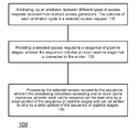
- FIG. 3 is a flow chart of method 100 for servicing access requests, according to an embodiment of the invention.
- Method 100 starts by stage 110 of arbitrating, by an arbitrator, between different types of access requests received from multiple access generators.
- the outcome of each arbitration cycle is a selected access request.
- Stage 110 is followed by stage 120 of providing a selected access request to a sequence of pipeline stages; wherein the sequence includes an input pipeline stage that is connected to the arbiter.
- Stage 120 is followed by stage 130 of processing the selected access request by the sequence.
- the processing includes accessing one or more cache resources.
- Each cache resource can be read only by a small portion of the sequence of pipeline stages and can be written to only by a small portion of the sequence of pipeline stages.
- sequence 30 of pipeline stages 30 ( 1 )- 30 (K) processes the selected access request.
- the processing can include accessing one or more cache memory resources.
- FIG. 4 illustrates method 200 for designing a cache memory according to an embodiment of the invention. It is assumed that method 200 is aimed to update an existing design of a memory cache.
- the existing memory cache can support certain access types and the purpose of method 200 is to add another supported access type.
- Method 200 starts by stage 210 of receiving or altering a design of a cache module.
- Stage 210 is followed by stage 220 of receiving a request to update a design of a cache memory such as to support a new access type.
- the cache memory is adapted to support certain access types.
- the cache memory includes an arbitrator that is connected to multiple access generators.
- the arbitrator is adapted to receive certain types of access requests from the multiple access generators and to select a single request per arbitration cycle.
- the arbitrator is also connected to an input pipeline stage of a sequence of pipeline stages.
- the sequence of pipeline stages is connected to multiple cache resources, such that each cache resource can be read only by a small portion of the sequence of pipeline stages and can be written to only by a small portion of the sequence of pipeline stages.
- Stage 220 is followed by stage 230 of altering an arbitration scheme of an arbitrator such as to arbitrate between the certain access types and the new access type.
- Stage 230 can also include configuring the pipeline cache to support the new access type. The configuration can include deciding which pipeline stage should access which resources in order to support the new access type.
- method 200 can be implemented by a processor that can execute a computer code that is stored within a computer readable memory. Accordingly, a computer program product is provided.
- the computer program product includes a computer readable memory that stored code that once executed by a processor can implement method 200 .
Abstract
Description
| TABLE 1 | ||||
| Cache resource | Hit/miss | Tag | dirty | Data |
| Pipeline stage \ | calculation | memory | memory | memory |
| Hazard detection | ||||
| Hit/miss | W & R | R | ||
| evaluation | ||||
| Tag update | W | |||
| Thrash | R | R | ||
| Fetch | W | |||
| Set dirty | W | |||
| Write data | W | |||
| Drive data read | R | |||
| TABLE 2 | ||||
| Pre-fetch | ||||
| (SW & HW | ||||
| \ Access type | Read | Write | Sweep(data | pre- |
| Pipeline stage \ | access | access | coherency) | fetch) |
| Hazard detection | + | + | − | + |
| Hit/miss | + | + | − | + |
| evaluation | ||||
| Tag update | Upon | Upon | − | Upon miss |
| miss | miss | |||
| Thrash | Upon | Upon | + | Upon miss |
| miss | miss | |||
| Fetch | Upon | − | − | + |
| miss | ||||
| Set dirty | − | + | − | − |
| Drive data read | + | − | − | − |
Claims (17)
Priority Applications (1)
| Application Number | Priority Date | Filing Date | Title |
|---|---|---|---|
| US11/849,375 US8103833B2 (en) | 2007-09-04 | 2007-09-04 | Cache memory and a method for servicing access requests |
Applications Claiming Priority (1)
| Application Number | Priority Date | Filing Date | Title |
|---|---|---|---|
| US11/849,375 US8103833B2 (en) | 2007-09-04 | 2007-09-04 | Cache memory and a method for servicing access requests |
Publications (2)
| Publication Number | Publication Date |
|---|---|
| US20090063779A1 US20090063779A1 (en) | 2009-03-05 |
| US8103833B2 true US8103833B2 (en) | 2012-01-24 |
Family
ID=40409303
Family Applications (1)
| Application Number | Title | Priority Date | Filing Date |
|---|---|---|---|
| US11/849,375 Expired - Fee Related US8103833B2 (en) | 2007-09-04 | 2007-09-04 | Cache memory and a method for servicing access requests |
Country Status (1)
| Country | Link |
|---|---|
| US (1) | US8103833B2 (en) |
Cited By (6)
| Publication number | Priority date | Publication date | Assignee | Title |
|---|---|---|---|---|
| US20140046979A1 (en) * | 2012-08-09 | 2014-02-13 | Fujitsu Limited | Computational processing device, information processing device, and method of controlling information processing device |
| CN105934743A (en) * | 2014-12-13 | 2016-09-07 | 上海兆芯集成电路有限公司 | Conditional pattern detector for detecting hangs |
| US9946651B2 (en) | 2014-12-13 | 2018-04-17 | Via Alliance Semiconductor Co., Ltd | Pattern detector for detecting hangs |
| US10067871B2 (en) | 2014-12-13 | 2018-09-04 | Via Alliance Semiconductor Co., Ltd | Logic analyzer for detecting hangs |
| US10324842B2 (en) | 2014-12-13 | 2019-06-18 | Via Alliance Semiconductor Co., Ltd | Distributed hang recovery logic |
| US20220083490A1 (en) * | 2020-09-15 | 2022-03-17 | Fujitsu Limited | Semiconductor apparatus and transfer method |
Families Citing this family (2)
| Publication number | Priority date | Publication date | Assignee | Title |
|---|---|---|---|---|
| US10477194B2 (en) | 2012-04-25 | 2019-11-12 | 3M Innovative Properties Company | Two imager projection device |
| US10901909B2 (en) * | 2017-04-17 | 2021-01-26 | Intel Corporation | Optimizing read only memory surface accesses |
Citations (11)
| Publication number | Priority date | Publication date | Assignee | Title |
|---|---|---|---|---|
| EP0833065A1 (en) | 1996-09-26 | 1998-04-01 | Fischerwerke Arthur Fischer GmbH & Co. KG | Compound plug |
| US5983023A (en) * | 1997-01-17 | 1999-11-09 | Mitsubishi Denki Kabushiki Kaisha | Memory-contained processor |
| US6023748A (en) * | 1997-09-12 | 2000-02-08 | Adaptec, Inc. | Multiple client memory arbitration system capable of operating multiple configuration types |
| US6055579A (en) * | 1997-11-17 | 2000-04-25 | Silicon Graphics, Inc. | Distributed control and synchronization of multiple data processors using flexible command queues |
| US6088789A (en) * | 1998-05-13 | 2000-07-11 | Advanced Micro Devices, Inc. | Prefetch instruction specifying destination functional unit and read/write access mode |
| US6148371A (en) * | 1997-06-25 | 2000-11-14 | Sun Microsystems, Inc. | Multi-level non-blocking cache system with inhibiting thrashing |
| US6151664A (en) * | 1999-06-09 | 2000-11-21 | International Business Machines Corporation | Programmable SRAM and DRAM cache interface with preset access priorities |
| GB2389206A (en) | 2002-03-20 | 2003-12-03 | Hewlett Packard Co | Cache control using queues to buffer requests and data |
| US20060059312A1 (en) * | 2004-09-14 | 2006-03-16 | Itay Peled | System and method for fetching information in response to hazard indication information |
| US20060064552A9 (en) * | 2002-04-24 | 2006-03-23 | Ip-First, Llc. | Cache memory and method for handling effects of external snoops colliding with in-flight operations internally to the cache |
| US20070011382A1 (en) * | 2003-05-09 | 2007-01-11 | Koninklijke Philips Electronics N.V. | Hierarchical memory access via pipelining with deferred arbitration |
-
2007
- 2007-09-04 US US11/849,375 patent/US8103833B2/en not_active Expired - Fee Related
Patent Citations (11)
| Publication number | Priority date | Publication date | Assignee | Title |
|---|---|---|---|---|
| EP0833065A1 (en) | 1996-09-26 | 1998-04-01 | Fischerwerke Arthur Fischer GmbH & Co. KG | Compound plug |
| US5983023A (en) * | 1997-01-17 | 1999-11-09 | Mitsubishi Denki Kabushiki Kaisha | Memory-contained processor |
| US6148371A (en) * | 1997-06-25 | 2000-11-14 | Sun Microsystems, Inc. | Multi-level non-blocking cache system with inhibiting thrashing |
| US6023748A (en) * | 1997-09-12 | 2000-02-08 | Adaptec, Inc. | Multiple client memory arbitration system capable of operating multiple configuration types |
| US6055579A (en) * | 1997-11-17 | 2000-04-25 | Silicon Graphics, Inc. | Distributed control and synchronization of multiple data processors using flexible command queues |
| US6088789A (en) * | 1998-05-13 | 2000-07-11 | Advanced Micro Devices, Inc. | Prefetch instruction specifying destination functional unit and read/write access mode |
| US6151664A (en) * | 1999-06-09 | 2000-11-21 | International Business Machines Corporation | Programmable SRAM and DRAM cache interface with preset access priorities |
| GB2389206A (en) | 2002-03-20 | 2003-12-03 | Hewlett Packard Co | Cache control using queues to buffer requests and data |
| US20060064552A9 (en) * | 2002-04-24 | 2006-03-23 | Ip-First, Llc. | Cache memory and method for handling effects of external snoops colliding with in-flight operations internally to the cache |
| US20070011382A1 (en) * | 2003-05-09 | 2007-01-11 | Koninklijke Philips Electronics N.V. | Hierarchical memory access via pipelining with deferred arbitration |
| US20060059312A1 (en) * | 2004-09-14 | 2006-03-16 | Itay Peled | System and method for fetching information in response to hazard indication information |
Cited By (11)
| Publication number | Priority date | Publication date | Assignee | Title |
|---|---|---|---|---|
| US20140046979A1 (en) * | 2012-08-09 | 2014-02-13 | Fujitsu Limited | Computational processing device, information processing device, and method of controlling information processing device |
| US9483502B2 (en) * | 2012-08-09 | 2016-11-01 | Fujitsu Limited | Computational processing device including request holding units each provided for each type of commands, information processing device including request holding units each provided for each type of commands, and method of controlling information processing device |
| CN105934743A (en) * | 2014-12-13 | 2016-09-07 | 上海兆芯集成电路有限公司 | Conditional pattern detector for detecting hangs |
| US20160350167A1 (en) * | 2014-12-13 | 2016-12-01 | Via Alliance Semiconductor Co., Ltd. | Conditional pattern detector for detecting hangs |
| US9753799B2 (en) * | 2014-12-13 | 2017-09-05 | Via Alliance Semiconductor Co., Ltd. | Conditional pattern detector for detecting hangs |
| US9946651B2 (en) | 2014-12-13 | 2018-04-17 | Via Alliance Semiconductor Co., Ltd | Pattern detector for detecting hangs |
| US10067871B2 (en) | 2014-12-13 | 2018-09-04 | Via Alliance Semiconductor Co., Ltd | Logic analyzer for detecting hangs |
| CN105934743B (en) * | 2014-12-13 | 2019-06-04 | 上海兆芯集成电路有限公司 | A kind of microprocessor and the method in the mode for wherein detecting arb |
| US10324842B2 (en) | 2014-12-13 | 2019-06-18 | Via Alliance Semiconductor Co., Ltd | Distributed hang recovery logic |
| US20220083490A1 (en) * | 2020-09-15 | 2022-03-17 | Fujitsu Limited | Semiconductor apparatus and transfer method |
| US11914538B2 (en) * | 2020-09-15 | 2024-02-27 | Fujitsu Limited | Semiconductor apparatus and transfer method |
Also Published As
| Publication number | Publication date |
|---|---|
| US20090063779A1 (en) | 2009-03-05 |
Similar Documents
| Publication | Publication Date | Title |
|---|---|---|
| US8103833B2 (en) | Cache memory and a method for servicing access requests | |
| US8478950B2 (en) | Data processing circuit with arbitration between a plurality of queues | |
| US7418576B1 (en) | Prioritized issuing of operation dedicated execution unit tagged instructions from multiple different type threads performing different set of operations | |
| US8082420B2 (en) | Method and apparatus for executing instructions | |
| US10503670B2 (en) | Dynamic per-bank and all-bank refresh | |
| US7426621B2 (en) | Memory access request arbitration | |
| US20100169578A1 (en) | Cache tag memory | |
| US10866902B2 (en) | Memory aware reordered source | |
| EP4200713A1 (en) | Memory controller with a plurality of command sub-queues and corresponding arbiters | |
| GB2529180A (en) | Arbitration and hazard detection for a data processing apparatus | |
| JPH09244952A (en) | System for holding band width to main memory | |
| US7725659B2 (en) | Alignment of cache fetch return data relative to a thread | |
| US20060041721A1 (en) | System, apparatus and method for generating nonsequential predictions to access a memory | |
| US20130212364A1 (en) | Pre-scheduled replays of divergent operations | |
| US9367464B2 (en) | Cache circuit having a tag array with smaller latency than a data array | |
| US8205064B2 (en) | Latency hiding for a memory management unit page table lookup | |
| US8006042B2 (en) | Floating point bypass retry | |
| US8977815B2 (en) | Control of entry of program instructions to a fetch stage within a processing pipepline | |
| US20100095071A1 (en) | Cache control apparatus and cache control method | |
| US20090083490A1 (en) | System to Improve Data Store Throughput for a Shared-Cache of a Multiprocessor Structure and Associated Methods | |
| US20140173225A1 (en) | Reducing memory access time in parallel processors | |
| US7650483B2 (en) | Execution of instructions within a data processing apparatus having a plurality of processing units | |
| US8180970B2 (en) | Least recently used (LRU) compartment capture in a cache memory system | |
| US9817668B2 (en) | Batched replays of divergent operations | |
| US10303483B2 (en) | Arithmetic processing unit and control method for arithmetic processing unit |
Legal Events
| Date | Code | Title | Description |
|---|---|---|---|
| AS | Assignment |
Owner name: FREESCALE SEMICONDUCTOR, INC., TEXAS Free format text: ASSIGNMENT OF ASSIGNORS INTEREST;ASSIGNORS:KOREN, SHAI, MR.;ELDAR, ALON, MR.;GUR, AMIT, MR.;AND OTHERS;REEL/FRAME:019776/0507;SIGNING DATES FROM 20070826 TO 20070827 Owner name: FREESCALE SEMICONDUCTOR, INC., TEXAS Free format text: ASSIGNMENT OF ASSIGNORS INTEREST;ASSIGNORS:KOREN, SHAI, MR.;ELDAR, ALON, MR.;GUR, AMIT, MR.;AND OTHERS;SIGNING DATES FROM 20070826 TO 20070827;REEL/FRAME:019776/0507 |
|
| AS | Assignment |
Owner name: CITIBANK, N.A.,NEW YORK Free format text: SECURITY AGREEMENT;ASSIGNOR:FREESCALE SEMICONDUCTOR, INC.;REEL/FRAME:020518/0215 Effective date: 20071025 Owner name: CITIBANK, N.A., NEW YORK Free format text: SECURITY AGREEMENT;ASSIGNOR:FREESCALE SEMICONDUCTOR, INC.;REEL/FRAME:020518/0215 Effective date: 20071025 |
|
| AS | Assignment |
Owner name: CITIBANK, N.A.,NEW YORK Free format text: SECURITY AGREEMENT;ASSIGNOR:FREESCALE SEMICONDUCTOR, INC.;REEL/FRAME:024085/0001 Effective date: 20100219 Owner name: CITIBANK, N.A., NEW YORK Free format text: SECURITY AGREEMENT;ASSIGNOR:FREESCALE SEMICONDUCTOR, INC.;REEL/FRAME:024085/0001 Effective date: 20100219 |
|
| AS | Assignment |
Owner name: CITIBANK, N.A., AS COLLATERAL AGENT,NEW YORK Free format text: SECURITY AGREEMENT;ASSIGNOR:FREESCALE SEMICONDUCTOR, INC.;REEL/FRAME:024397/0001 Effective date: 20100413 Owner name: CITIBANK, N.A., AS COLLATERAL AGENT, NEW YORK Free format text: SECURITY AGREEMENT;ASSIGNOR:FREESCALE SEMICONDUCTOR, INC.;REEL/FRAME:024397/0001 Effective date: 20100413 |
|
| FEPP | Fee payment procedure |
Free format text: PAYOR NUMBER ASSIGNED (ORIGINAL EVENT CODE: ASPN); ENTITY STATUS OF PATENT OWNER: LARGE ENTITY |
|
| STCF | Information on status: patent grant |
Free format text: PATENTED CASE |
|
| AS | Assignment |
Owner name: CITIBANK, N.A., AS NOTES COLLATERAL AGENT, NEW YOR Free format text: SECURITY AGREEMENT;ASSIGNOR:FREESCALE SEMICONDUCTOR, INC.;REEL/FRAME:030633/0424 Effective date: 20130521 |
|
| AS | Assignment |
Owner name: CITIBANK, N.A., AS NOTES COLLATERAL AGENT, NEW YOR Free format text: SECURITY AGREEMENT;ASSIGNOR:FREESCALE SEMICONDUCTOR, INC.;REEL/FRAME:031591/0266 Effective date: 20131101 |
|
| FPAY | Fee payment |
Year of fee payment: 4 |
|
| AS | Assignment |
Owner name: FREESCALE SEMICONDUCTOR, INC., TEXAS Free format text: PATENT RELEASE;ASSIGNOR:CITIBANK, N.A., AS COLLATERAL AGENT;REEL/FRAME:037354/0704 Effective date: 20151207 Owner name: FREESCALE SEMICONDUCTOR, INC., TEXAS Free format text: PATENT RELEASE;ASSIGNOR:CITIBANK, N.A., AS COLLATERAL AGENT;REEL/FRAME:037356/0553 Effective date: 20151207 Owner name: FREESCALE SEMICONDUCTOR, INC., TEXAS Free format text: PATENT RELEASE;ASSIGNOR:CITIBANK, N.A., AS COLLATERAL AGENT;REEL/FRAME:037356/0143 Effective date: 20151207 |
|
| AS | Assignment |
Owner name: MORGAN STANLEY SENIOR FUNDING, INC., MARYLAND Free format text: ASSIGNMENT AND ASSUMPTION OF SECURITY INTEREST IN PATENTS;ASSIGNOR:CITIBANK, N.A.;REEL/FRAME:037486/0517 Effective date: 20151207 |
|
| AS | Assignment |
Owner name: MORGAN STANLEY SENIOR FUNDING, INC., MARYLAND Free format text: ASSIGNMENT AND ASSUMPTION OF SECURITY INTEREST IN PATENTS;ASSIGNOR:CITIBANK, N.A.;REEL/FRAME:037518/0292 Effective date: 20151207 |
|
| AS | Assignment |
Owner name: MORGAN STANLEY SENIOR FUNDING, INC., MARYLAND Free format text: SECURITY AGREEMENT SUPPLEMENT;ASSIGNOR:NXP B.V.;REEL/FRAME:038017/0058 Effective date: 20160218 |
|
| AS | Assignment |
Owner name: MORGAN STANLEY SENIOR FUNDING, INC., MARYLAND Free format text: SUPPLEMENT TO THE SECURITY AGREEMENT;ASSIGNOR:FREESCALE SEMICONDUCTOR, INC.;REEL/FRAME:039138/0001 Effective date: 20160525 |
|
| AS | Assignment |
Owner name: MORGAN STANLEY SENIOR FUNDING, INC., MARYLAND Free format text: CORRECTIVE ASSIGNMENT TO CORRECT THE REMOVE APPLICATION 12092129 PREVIOUSLY RECORDED ON REEL 038017 FRAME 0058. ASSIGNOR(S) HEREBY CONFIRMS THE SECURITY AGREEMENT SUPPLEMENT;ASSIGNOR:NXP B.V.;REEL/FRAME:039361/0212 Effective date: 20160218 |
|
| AS | Assignment |
Owner name: NXP, B.V., F/K/A FREESCALE SEMICONDUCTOR, INC., NETHERLANDS Free format text: RELEASE BY SECURED PARTY;ASSIGNOR:MORGAN STANLEY SENIOR FUNDING, INC.;REEL/FRAME:040925/0001 Effective date: 20160912 Owner name: NXP, B.V., F/K/A FREESCALE SEMICONDUCTOR, INC., NE Free format text: RELEASE BY SECURED PARTY;ASSIGNOR:MORGAN STANLEY SENIOR FUNDING, INC.;REEL/FRAME:040925/0001 Effective date: 20160912 |
|
| AS | Assignment |
Owner name: NXP B.V., NETHERLANDS Free format text: RELEASE BY SECURED PARTY;ASSIGNOR:MORGAN STANLEY SENIOR FUNDING, INC.;REEL/FRAME:040928/0001 Effective date: 20160622 |
|
| AS | Assignment |
Owner name: NXP USA, INC., TEXAS Free format text: CHANGE OF NAME;ASSIGNOR:FREESCALE SEMICONDUCTOR, INC.;REEL/FRAME:040632/0001 Effective date: 20161107 |
|
| AS | Assignment |
Owner name: MORGAN STANLEY SENIOR FUNDING, INC., MARYLAND Free format text: CORRECTIVE ASSIGNMENT TO CORRECT THE REMOVE PATENTS 8108266 AND 8062324 AND REPLACE THEM WITH 6108266 AND 8060324 PREVIOUSLY RECORDED ON REEL 037518 FRAME 0292. ASSIGNOR(S) HEREBY CONFIRMS THE ASSIGNMENT AND ASSUMPTION OF SECURITY INTEREST IN PATENTS;ASSIGNOR:CITIBANK, N.A.;REEL/FRAME:041703/0536 Effective date: 20151207 |
|
| AS | Assignment |
Owner name: MORGAN STANLEY SENIOR FUNDING, INC., MARYLAND Free format text: CORRECTIVE ASSIGNMENT TO CORRECT THE REMOVE APPLICATION 12681366 PREVIOUSLY RECORDED ON REEL 039361 FRAME 0212. ASSIGNOR(S) HEREBY CONFIRMS THE SECURITY AGREEMENT SUPPLEMENT;ASSIGNOR:NXP B.V.;REEL/FRAME:042762/0145 Effective date: 20160218 Owner name: MORGAN STANLEY SENIOR FUNDING, INC., MARYLAND Free format text: CORRECTIVE ASSIGNMENT TO CORRECT THE REMOVE APPLICATION 12681366 PREVIOUSLY RECORDED ON REEL 038017 FRAME 0058. ASSIGNOR(S) HEREBY CONFIRMS THE SECURITY AGREEMENT SUPPLEMENT;ASSIGNOR:NXP B.V.;REEL/FRAME:042985/0001 Effective date: 20160218 |
|
| AS | Assignment |
Owner name: NXP USA, INC., TEXAS Free format text: CORRECTIVE ASSIGNMENT TO CORRECT THE NATURE OF CONVEYANCE PREVIOUSLY RECORDED AT REEL: 040632 FRAME: 0001. ASSIGNOR(S) HEREBY CONFIRMS THE MERGER AND CHANGE OF NAME;ASSIGNOR:FREESCALE SEMICONDUCTOR INC.;REEL/FRAME:044209/0047 Effective date: 20161107 |
|
| AS | Assignment |
Owner name: SHENZHEN XINGUODU TECHNOLOGY CO., LTD., CHINA Free format text: CORRECTIVE ASSIGNMENT TO CORRECT THE TO CORRECT THE APPLICATION NO. FROM 13,883,290 TO 13,833,290 PREVIOUSLY RECORDED ON REEL 041703 FRAME 0536. ASSIGNOR(S) HEREBY CONFIRMS THE THE ASSIGNMENT AND ASSUMPTION OF SECURITYINTEREST IN PATENTS.;ASSIGNOR:MORGAN STANLEY SENIOR FUNDING, INC.;REEL/FRAME:048734/0001 Effective date: 20190217 |
|
| AS | Assignment |
Owner name: NXP B.V., NETHERLANDS Free format text: RELEASE BY SECURED PARTY;ASSIGNOR:MORGAN STANLEY SENIOR FUNDING, INC.;REEL/FRAME:050745/0001 Effective date: 20190903 Owner name: NXP B.V., NETHERLANDS Free format text: RELEASE BY SECURED PARTY;ASSIGNOR:MORGAN STANLEY SENIOR FUNDING, INC.;REEL/FRAME:050744/0097 Effective date: 20190903 |
|
| FEPP | Fee payment procedure |
Free format text: MAINTENANCE FEE REMINDER MAILED (ORIGINAL EVENT CODE: REM.); ENTITY STATUS OF PATENT OWNER: LARGE ENTITY |
|
| AS | Assignment |
Owner name: MORGAN STANLEY SENIOR FUNDING, INC., MARYLAND Free format text: CORRECTIVE ASSIGNMENT TO CORRECT THE REMOVE APPLICATION 12298143 PREVIOUSLY RECORDED ON REEL 042985 FRAME 0001. ASSIGNOR(S) HEREBY CONFIRMS THE SECURITY AGREEMENT SUPPLEMENT;ASSIGNOR:NXP B.V.;REEL/FRAME:051029/0001 Effective date: 20160218 Owner name: MORGAN STANLEY SENIOR FUNDING, INC., MARYLAND Free format text: CORRECTIVE ASSIGNMENT TO CORRECT THE REMOVE APPLICATION 12298143 PREVIOUSLY RECORDED ON REEL 042762 FRAME 0145. ASSIGNOR(S) HEREBY CONFIRMS THE SECURITY AGREEMENT SUPPLEMENT;ASSIGNOR:NXP B.V.;REEL/FRAME:051145/0184 Effective date: 20160218 Owner name: MORGAN STANLEY SENIOR FUNDING, INC., MARYLAND Free format text: CORRECTIVE ASSIGNMENT TO CORRECT THE REMOVE APPLICATION 12298143 PREVIOUSLY RECORDED ON REEL 039361 FRAME 0212. ASSIGNOR(S) HEREBY CONFIRMS THE SECURITY AGREEMENT SUPPLEMENT;ASSIGNOR:NXP B.V.;REEL/FRAME:051029/0387 Effective date: 20160218 Owner name: MORGAN STANLEY SENIOR FUNDING, INC., MARYLAND Free format text: CORRECTIVE ASSIGNMENT TO CORRECT THE REMOVE APPLICATION12298143 PREVIOUSLY RECORDED ON REEL 039361 FRAME 0212. ASSIGNOR(S) HEREBY CONFIRMS THE SECURITY AGREEMENT SUPPLEMENT;ASSIGNOR:NXP B.V.;REEL/FRAME:051029/0387 Effective date: 20160218 Owner name: MORGAN STANLEY SENIOR FUNDING, INC., MARYLAND Free format text: CORRECTIVE ASSIGNMENT TO CORRECT THE REMOVE APPLICATION 12298143 PREVIOUSLY RECORDED ON REEL 038017 FRAME 0058. ASSIGNOR(S) HEREBY CONFIRMS THE SECURITY AGREEMENT SUPPLEMENT;ASSIGNOR:NXP B.V.;REEL/FRAME:051030/0001 Effective date: 20160218 Owner name: MORGAN STANLEY SENIOR FUNDING, INC., MARYLAND Free format text: CORRECTIVE ASSIGNMENT TO CORRECT THE REMOVE APPLICATION12298143 PREVIOUSLY RECORDED ON REEL 042985 FRAME 0001. ASSIGNOR(S) HEREBY CONFIRMS THE SECURITY AGREEMENT SUPPLEMENT;ASSIGNOR:NXP B.V.;REEL/FRAME:051029/0001 Effective date: 20160218 Owner name: MORGAN STANLEY SENIOR FUNDING, INC., MARYLAND Free format text: CORRECTIVE ASSIGNMENT TO CORRECT THE REMOVE APPLICATION12298143 PREVIOUSLY RECORDED ON REEL 042762 FRAME 0145. ASSIGNOR(S) HEREBY CONFIRMS THE SECURITY AGREEMENT SUPPLEMENT;ASSIGNOR:NXP B.V.;REEL/FRAME:051145/0184 Effective date: 20160218 |
|
| AS | Assignment |
Owner name: MORGAN STANLEY SENIOR FUNDING, INC., MARYLAND Free format text: CORRECTIVE ASSIGNMENT TO CORRECT THE REMOVE APPLICATION11759915 AND REPLACE IT WITH APPLICATION 11759935 PREVIOUSLY RECORDED ON REEL 037486 FRAME 0517. ASSIGNOR(S) HEREBY CONFIRMS THE ASSIGNMENT AND ASSUMPTION OF SECURITYINTEREST IN PATENTS;ASSIGNOR:CITIBANK, N.A.;REEL/FRAME:053547/0421 Effective date: 20151207 |
|
| AS | Assignment |
Owner name: NXP B.V., NETHERLANDS Free format text: CORRECTIVE ASSIGNMENT TO CORRECT THE REMOVEAPPLICATION 11759915 AND REPLACE IT WITH APPLICATION11759935 PREVIOUSLY RECORDED ON REEL 040928 FRAME 0001. ASSIGNOR(S) HEREBY CONFIRMS THE RELEASE OF SECURITYINTEREST;ASSIGNOR:MORGAN STANLEY SENIOR FUNDING, INC.;REEL/FRAME:052915/0001 Effective date: 20160622 |
|
| AS | Assignment |
Owner name: NXP, B.V. F/K/A FREESCALE SEMICONDUCTOR, INC., NETHERLANDS Free format text: CORRECTIVE ASSIGNMENT TO CORRECT THE REMOVEAPPLICATION 11759915 AND REPLACE IT WITH APPLICATION11759935 PREVIOUSLY RECORDED ON REEL 040925 FRAME 0001. ASSIGNOR(S) HEREBY CONFIRMS THE RELEASE OF SECURITYINTEREST;ASSIGNOR:MORGAN STANLEY SENIOR FUNDING, INC.;REEL/FRAME:052917/0001 Effective date: 20160912 |
|
| LAPS | Lapse for failure to pay maintenance fees |
Free format text: PATENT EXPIRED FOR FAILURE TO PAY MAINTENANCE FEES (ORIGINAL EVENT CODE: EXP.); ENTITY STATUS OF PATENT OWNER: LARGE ENTITY |
|
| STCH | Information on status: patent discontinuation |
Free format text: PATENT EXPIRED DUE TO NONPAYMENT OF MAINTENANCE FEES UNDER 37 CFR 1.362 |
|
| FP | Lapsed due to failure to pay maintenance fee |
Effective date: 20200124 |