US8204031B2 - Duplexer/multiplexer having filters that include at least one band reject filter - Google Patents
Duplexer/multiplexer having filters that include at least one band reject filter Download PDFInfo
- Publication number
- US8204031B2 US8204031B2 US12/237,098 US23709808A US8204031B2 US 8204031 B2 US8204031 B2 US 8204031B2 US 23709808 A US23709808 A US 23709808A US 8204031 B2 US8204031 B2 US 8204031B2
- Authority
- US
- United States
- Prior art keywords
- receive
- filter
- transmit
- wireless communications
- communications device
- Prior art date
- Legal status (The legal status is an assumption and is not a legal conclusion. Google has not performed a legal analysis and makes no representation as to the accuracy of the status listed.)
- Active, expires
Links
- 238000010897 surface acoustic wave method Methods 0.000 claims description 4
- 239000010409 thin film Substances 0.000 claims description 2
- 101100194362 Schizosaccharomyces pombe (strain 972 / ATCC 24843) res1 gene Proteins 0.000 description 12
- 101100194363 Schizosaccharomyces pombe (strain 972 / ATCC 24843) res2 gene Proteins 0.000 description 11
- 238000010586 diagram Methods 0.000 description 10
- 238000003780 insertion Methods 0.000 description 4
- 230000037431 insertion Effects 0.000 description 4
- 238000013508 migration Methods 0.000 description 4
- 238000005516 engineering process Methods 0.000 description 3
- 238000012986 modification Methods 0.000 description 3
- 230000004048 modification Effects 0.000 description 3
- 230000002238 attenuated effect Effects 0.000 description 2
- 230000005540 biological transmission Effects 0.000 description 2
- 230000007774 longterm Effects 0.000 description 2
- 239000003990 capacitor Substances 0.000 description 1
- 230000006866 deterioration Effects 0.000 description 1
- 230000000694 effects Effects 0.000 description 1
- 238000011156 evaluation Methods 0.000 description 1
- 239000002184 metal Substances 0.000 description 1
Images


Classifications
-
- H—ELECTRICITY
- H04—ELECTRIC COMMUNICATION TECHNIQUE
- H04B—TRANSMISSION
- H04B1/00—Details of transmission systems, not covered by a single one of groups H04B3/00 - H04B13/00; Details of transmission systems not characterised by the medium used for transmission
- H04B1/005—Details of transmission systems, not covered by a single one of groups H04B3/00 - H04B13/00; Details of transmission systems not characterised by the medium used for transmission adapting radio receivers, transmitters andtransceivers for operation on two or more bands, i.e. frequency ranges
- H04B1/0053—Details of transmission systems, not covered by a single one of groups H04B3/00 - H04B13/00; Details of transmission systems not characterised by the medium used for transmission adapting radio receivers, transmitters andtransceivers for operation on two or more bands, i.e. frequency ranges with common antenna for more than one band
- H04B1/0057—Details of transmission systems, not covered by a single one of groups H04B3/00 - H04B13/00; Details of transmission systems not characterised by the medium used for transmission adapting radio receivers, transmitters andtransceivers for operation on two or more bands, i.e. frequency ranges with common antenna for more than one band using diplexing or multiplexing filters for selecting the desired band
Definitions
- the invention relates generally to a duplexer/multiplexer that has filters including at least one band reject filter.
- Wireless communications devices such as wireless terminals or wireless base stations, include wireless transceivers to perform wireless communications, such as radio frequency (RF) communications.
- a wireless communications device can include a duplexer (or multiplexer) to allow simultaneous transmission and reception in different frequency bands using the same antenna while ensuring that relatively high power transmit signals transmitted by the wireless transceiver do not swamp relatively low power receive signals received by the wireless transceiver.
- a duplexer has an antenna port (for connection to an antenna), a receive port (to receive a signal from the antenna port) and transmit port (to transmit a signal to the antenna port).
- a multiplexer has an antenna port and one or more receive ports and one or more transmit ports. Note that a duplexer is a type of multiplexer.
- a duplexer or multiplexer can include bandpass filters implemented with acoustic-type resonators.
- Conventional duplexers/multiplexers including bandpass filters implemented with acoustic-type resonators have relatively limited maximum power handling capabilities, which can prevent use of such conventional duplexers/multiplexers in high-power, high-frequency applications, such as in Worldwide Interoperability for Microwave Access (WiMax) applications or Long-Term Evolution (LTE) applications.
- WiMax is based on the IEEE (Institute of Electrical and Electronics Engineers) 802.16 Standard (as amended by the IEEE 802.16e or IEEE 802.16e-005). WiMax is able to provide broadband wireless connectivity for mobile stations at relatively high data rates.
- LTE is a technology that provides an enhancement to the Universal Mobile Telecommunications System (UMTS) technology. LTE is described in 3GPP TS 23.401 and 23.402.
- a wireless communications device includes an antenna and a multi-port path selection structure (e.g., a duplexer or multiplexer) having an antenna port connected to the antenna, and plural ports connected to respective receive and transmit paths of the wireless communications device.
- the multi-port path selection structure has a band reject filter connected to the transmit path and a second filter connected to the receive path.
- FIG. 1 is a block diagram of a wireless communications device that includes a duplexer or multiplexer according to an embodiment.
- FIG. 2 is a schematic diagram of a conventional duplexer that includes bandpass filters connected to a receive port and a transmit port of the duplexer.
- FIG. 3 is a graph illustrating the transmit and receive bands provided by the bandpass filters of FIG. 2 .
- FIG. 4 is a schematic diagram of a duplexer that includes a receive filter connected to a receive port, and a band reject filter connected to a transmit port, according to an embodiment.
- FIG. 5 is a graph illustrating the transmit and receive bands provided by the filters of FIG. 4 .
- FIG. 6 illustrates acoustic-type resonators arranged in a ladder-type configuration for implementing a band reject filter for use in a duplexer or multiplexer according to an embodiment.
- FIG. 7 is a graph illustrating the resonance and anti-resonance frequencies of the resonators of FIG. 6 .
- FIG. 8 is a schematic diagram of a duplexer according to another embodiment that includes a band reject filter connected to a receive port, and a band reject filter connected to a transmit port.
- FIG. 9 is a graph illustrating the transmit and receive bands provided by the filters of FIG. 8 .
- FIG. 10 is a schematic diagram of a multiplexer that includes bandpass filters connected to receive ports, and band reject filters connected to transmit ports, according to another embodiment.
- FIG. 11 is a graph illustrating the transmit and receive bands provided by the filters of FIG. 10 .
- FIG. 12 is a schematic diagram of a multiplexer that includes bandpass filters connected to receive ports, and a band reject filter connected to a transmit port, according to a further embodiment.
- FIG. 13 is a graph illustrating the transmit and receive bands provided by the filters of FIG. 12 .
- FIG. 14 is a schematic diagram of a band reject filter formed of cascaded band reject filter units to provide multiple reject bands, according to an embodiment.
- FIG. 15 is a graph illustrating the multiple reject bands provided by the band reject filter of FIG. 14 .
- FIG. 16 is a schematic diagram of a duplexer according to a further embodiment that includes a bandpass filter connected to a receive port, and a band reject filter connected to a transmit port.
- FIG. 17 is a graph illustrating the transmit and receive bands provided by the filters of FIG. 16 .
- FIG. 18 is a schematic diagram of a duplexer according to yet a further embodiment that includes a band reject filter connected to a receive port, and a band reject filter connected to a transmit port.
- FIG. 19 is a graph illustrating the transmit and receive bands provided by the filters of FIG. 18 .
- FIG. 20 is a schematic diagram of a multiplexer that includes a band reject filter connected to a receive port, and a band reject filter connected to a transmit port, according to a further embodiment.
- FIG. 21 is a graph illustrating the transmit and receive bands provided by the filters of FIG. 20 .
- a multi-port path selection structure for use in a wireless communications device has an antenna port connected to an antenna of the wireless communications device, and plural ports connected to respective receive and transmit paths of the wireless communications device.
- the wireless communications device include a wireless terminal (mobile station), a wireless base station, and other devices that are capable of performing wireless communications.
- a multi-port path selection structure can be a duplexer or a multiplexer.
- a multi-port path selection structure includes circuitry to selectively route signals that are communicated along transmit and receive paths of the wireless communications device. Such circuitry can receive a signal from the antenna of the wireless communications device, and route the received signal to the receive path of the wireless communications device.
- the multi-port path selection structure can route a transmitted signal from transmission circuitry in the transmit path of the wireless communications device to the antenna.
- the “routing” of the received and transmitted signals is accomplished by use of filters provided in the multi-port path selection structure, where the filters are designed to pass signals in respective receive and transmit frequency bands.
- the filter connected to the transmit path is a band reject filter
- the filter connected to the receive path can either be a bandpass filter or band reject filter.
- a duplexer has an antenna port connected to the antenna of the wireless communications device, and a single receive port and a single transmit port for connection to respective receive and transmit paths of the wireless communications device.
- a multiplexer includes an antenna port for connection to the antenna of the wireless communications device, and two or more ports connected to respective receive and transmit paths. Note that a duplexer is a type of multiplexer.
- a multiplexer can have plural receive ports (corresponding to different receive frequency bands) and/or plural transmit ports (corresponding to different transmit frequency bands).
- the multiple receive ports can be connected to one or plural receive paths in the wireless communications device.
- the multiple transmit ports can be connected to one or plural transmit paths in the wireless communications device. Note that it is possible for multiple receive frequency bands and/or multiple transmit frequency bands to share just one receive path or transmit path, respectively, since a wireless communications device normally operates at just a single receive or transmit frequency band at any given time. Alternatively, separate paths in the wireless communications device can be provided for different receive frequency bands or different transmit frequency bands.
- FIG. 1 illustrates an exemplary wireless communications device 100 that includes a duplexer or multiplexer 102 according to an embodiment.
- the wireless communications device 100 has an antenna 104 for communicating radio frequency (RF) signals with another communications device.
- the wireless communications device 100 can be a wireless terminal (e.g., mobile station) to communicate wirelessly with a wireless base station.
- the wireless communications device 100 can be base station for communicating with a wireless terminal.
- the wireless communications device can be used in a wireless communications network, such as a WiMax (Worldwide Interoperability for Microwave Access) network, a Long-Term Evaluation (LTE) network, or any other type of network.
- a wireless communications network such as a WiMax (Worldwide Interoperability for Microwave Access) network, a Long-Term Evaluation (LTE) network, or any other type of network.
- LTE is to any technology based on LTE, such as defined by current standards 3GPP TS 23.401 and 23.402 or any subsequent standard.
- Reference to LTE can also refer to any subsequent standard derived from an evolution of LTE, whether or not such subsequent standard is referred to as “LTE” by name.
- the multiplexer 102 has an antenna port 106 that is connected to the antenna 104 .
- the antenna port 106 of the multiplexer 102 is “connected” to the antenna 104 either directly or indirectly (through other circuitry).
- the multiplexer also has a receive port 108 for connection to a receive path 110 of the wireless communications device 100 , and a transmit port 112 for connection to a transmit path 114 of the wireless communications device.
- the receive path 110 includes receive circuitry 116 to receive a signal from the antenna 104 through the multiplexer 102 .
- the transmit path 114 includes transmit circuitry 118 to generate a transmit signal to be sent through the multiplexer 102 onto the antenna 104 .
- the multiplexer 102 has filters 120 and 122 for passing signals in the receive and transmit frequency bands, respectively. Also shown in dashed profile is another filter 124 and another port 126 , where the other filter 124 and port 126 can be connected to a transmit path or a receive path, depending upon the specific configuration of the wireless communications device 100 .
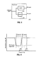
- a conventional duplexer 10 is depicted in FIG. 2 , where the conventional duplexer 10 has an antenna port 12 , a receive port 14 (that is connected to a receive path of a wireless communications device), and a transmit port 16 (that is connected to a transmit path of the wireless communications device).
- the conventional duplexer 10 uses bandpass filters (BPFs) 18 and 20 connected to the receive and transmit ports 14 and 16 , respectively.
- BPFs bandpass filters
- the bandpass filters 18 and 20 can be implemented with acoustic-type resonators.
- FIG. 3 is a graph of the transmit frequency band 22 and receive frequency band 24 provided by the bandpass filters 20 and 18 , respectively.
- the graph of FIG. 3 plots insertion loss (in terms of decibel or dB) as a function of frequency. Insertion loss is the decrease in signal power resulting from insertion of a device in a communications path.
- the bandpass filters 18 and 20 of a conventional duplexer such as duplexer 10 are subject to deterioration caused by the acousto-migration phenomenon at high power and high frequencies.
- a duplexer 200 (depicted in FIG. 4 ) can be provided that includes a band reject filter 202 connected to a transmit port of the duplexer 200 , and a receive filter 204 connected to a receive port of the duplexer 200 . Both the band reject filter 202 and receive filter 204 are connected to an antenna port.
- the receive filter 204 can either be a bandpass filter or a band reject filter, in accordance with some embodiments.
- the transmit signals that are sent from the transmit port to the antenna port through the duplexer 200 are associated with relatively high power, while the receive signals communicated from the antenna port to the receive port through the duplexer 200 are associated with relatively low power.
- the receive filter 204 operates to protect the receive port (and receive circuitry connected to the receive port) against the high-power transmit signals communicated through the duplexer 200 .
- the acoustic vibration is relatively strong in the reject band, but relatively weak in the pass band of the band reject filter. This enables the band reject filter 202 to handle relatively high power transmit signals with reduced acousto-migration issues.
- another characteristic of a band reject filter is that it has lower phase distortion and less ripple in the pass band, as compared to a bandpass filter.
- the bandpass filter 204 provides a pass band 302 —any signal having a frequency below or above the pass band 302 is attenuated or rejected by the bandpass filter 204 .
- the band reject filter 202 provides a reject band 304 —any signal having a frequency within the reject band 304 is attenuated or rejected, and any signal having a frequency above or below the reject band 304 is passed through the band reject filter 202 .
- the pass band 302 and reject band 304 of FIG. 5 overlap.
- the pass band for the transmit path provided by the band reject filter 202 is represented by reference numerals 306 A and 306 B, which are on the two sides of the reject band 304 (and of the pass band 302 provided by the bandpass filter 204 ).
- the bandpass filter 204 passes a signal from the antenna port to the receive port of the duplexer 200 if the signal has a frequency within the receive band 302 .
- the band reject filter 202 passes a signal having a frequency outside the reject band 304 through the band reject filter 202 from the transmit port to the antenna port.
- a band reject filter can be implemented with acoustic-type resonators RES 1 and RES 2 arranged in a ladder-type configuration, as depicted in FIG. 6 .
- the ladder-type configuration includes a first acoustic-type resonator RES 1 (referred to as “series resonator”) connected in series between two ports PORT 1 and PORT 2 , and a second acoustic-type resonator RES 2 (referred to as “shunt resonator”) connected between PORT 2 and ground.
- series resonator a first acoustic-type resonator RES 1
- shunt resonator a second acoustic-type resonator RES 2
- there can be two (or more) series resonators between PORT 1 and PORT 2 there can be two (or more) series resonators between PORT 1 and PORT 2 , and two (or more) shunt resonators connected between nodes of the filter and ground
- Each of the resonators RES 1 and RES 2 can be any one of a surface acoustic wave (SAW) resonator, a thin film bulk acoustic resonator (FBAR), a bulk acoustic wave (BAW) resonator, or any other type of acoustic-type resonator.
- the BAW resonator can be a surface mounted resonator (SMR)-type BAW resonator.
- the series resonator RES 1 of FIG. 6 is designed to present a high impedance at the reject band 304 of interest.
- the series resonator RES 1 is configured to be anti-resonance at a reject band frequency (the anti-resonance frequency for the series resonator RES 1 is depicted in FIG. 7 , according to one example), which means that the series resonator RES 1 presents a high impedance at the anti-resonance frequency.
- the shunt resonator RES 2 is configured to provide a low impedance at a reject band frequency (a frequency within reject band 304 ). This is achieved by designing the shunt resonator RES 2 to be at or near resonance in the reject band 304 .
- the resonance frequency of the shunt resonator RES 2 is represented as 404 in FIG. 7 .
- the resonance frequency of series resonator RES 1 is represented as 406 in FIG. 7
- the anti-resonance frequency of the shunt resonator RES 2 is represented as 408 in FIG. 7 .
- the resonance frequency 406 of the series resonator RES 1 is immediately below the reject band 304 and is between the pass band 306 A and the reject band 304 of the band reject filter—at the resonance frequency 406 , the series resonator RES 1 has a low impedance. In the pass band 306 A, the shunt resonator RES 2 simply presents a capacitive load to ground.
- the anti-resonance frequency 408 of the shunt resonator RES 2 is immediately above the reject band 304 and is between the reject band 304 and the pass band 306 B—at the anti-resonance frequency 408 , the shunt resonator RES 2 presents a high impedance to ground. However, in the pass band 306 B, the series resonator RES 1 presents a capacitive series impedance. At frequencies much above or below the reject band 304 , the series and shunt resonators simply behave as high-Q capacitors.
- the overall effect of the filter provided by resonators RES 1 and RES 2 is to provide a high impedance for signals passing between ports PORT 1 and PORT 2 having frequencies in the reject band 304 .
- FIG. 8 shows an implementation of the duplexer 200 in which the receive filter 204 is implemented with a band reject filter (instead of a bandpass filter as depicted in FIG. 4 ). In this configuration, both the receive and transmit ports of the duplexer 200 are connected to band reject filters.
- the band reject filter 202 for the transmit port is associated with the transmit reject band 304
- the band reject filter 204 for the receive port has a receive reject band 402 .
- the band reject filter 204 allows a signal having a frequency outside the receive reject band 402 to be passed through the band reject filter 204
- the band reject filter 202 allows a signal having a frequency outside the transmit reject band 304 to pass through the band reject filter 202 .
- FIG. 10 shows a multiplexer 500 that has an antenna port, two receive ports (RX 1 port and RX 2 port), and two transmit ports (TX 1 port and TX 2 port).
- the two receive ports can be connected to just one receive path (and the associated receive circuitry, such as circuitry 116 in FIG. 1 ), or alternatively, the two receive ports can be connected to two different receive paths.
- the transmit ports can be connected to just one transmit path (and the associated transmit circuitry, such as 118 in FIG. 1 ), or alternatively, the transmit ports can be connected to multiple transmit paths.
- the multiplexer 500 can have more than two transmit ports and/or more than two receive ports. The different receive ports are associated with different receive frequency bands, and the different transmit ports are associated with different transmit frequency bands.
- the receive ports of the multiplexer 500 are connected to corresponding bandpass filters 502 and 504 , whereas the transmit ports are connected to band reject filters 506 and 508 .
- Each of the bandpass filters and band reject filters 502 , 504 , 506 , and 508 is connected to the antenna port of the multiplexer 500 .
- a receive pass band 602 corresponds to the pass band provided by the bandpass filter 502 for the RX 1 port, and a receive pass band 604 is provided by the bandpass filter 504 for the RX 2 port.
- a transmit reject band 606 is provided by the band reject filter 506 for the TX 1 port, and a transmit reject band 608 is provided by the band reject filter 508 for the TX 2 port.
- FIG. 10 shows separate band reject filters 506 and 508 to provide two respective reject bands 606 and 608 ( FIG. 11 )
- a single band reject filter can be used instead, such as band reject filter 702 in a multiplexer 700 depicted in FIG. 12 , to provide multiple reject bands.
- the multiplexer 700 has one transmit port connected to the band reject filter 702 .
- the chart of FIG. 13 depicts receive pass bands 602 and 604 and transmit reject bands 606 and 608 that are the same as those depicted in FIG. 11 , except that the reject bands 606 and 608 of FIG. 13 are provided by one band reject filter 702 ( FIG. 12 ), instead of two distinct band reject filters 506 and 508 ( FIG. 10 ).
- the band reject filter 702 includes multiple cascaded band reject filter units to provide the multiple reject bands 606 and 608 .
- Cascading multiple band reject filter units means that the band reject filter units are connected in series.
- three band reject filter units 802 , 804 , and 806 are connected in series (cascaded) between PORT 1 and PORT 2 .
- Each of the band reject filter units 802 , 804 , and 806 defines a respective reject band, as depicted in FIG. 15 .
- the band reject filter unit 802 provides reject band 902
- the band reject filter unit 804 provides reject band 904
- the band reject filter unit 806 provides reject band 906 .
- Each of the band reject filter units contains an arrangement of resonators; in the embodiment of FIG. 14 , each band reject filter unit includes two series resonators and two shunt resonators arranged in the ladder-type configuration.
- two band reject filter units e.g., any two of 802 , 804 , and 806
- the resonators of all band reject filter units can be arranged in a mixed configuration for their locations in the ladder-type structure, namely each of the band reject filter units can have its resonators distributed in the entire filter structure and does not have to have all its resonators arranged together.
- FIG. 16 shows an alternative embodiment of a duplexer 1000 that has a band reject filter 1002 for the transmit port that provides multiple reject bands 1102 , 1104 , and 1106 ( FIG. 17 ).
- the band reject filter 1002 is thus able to block signals having frequencies in any of the reject bands 1102 , 1104 , and 1106 .
- a bandpass filter 1004 connected to the receive port of the duplexer 1000 provides a pass band 1108 ( FIG. 17 ).
- FIG. 18 shows another embodiment of a duplexer 1200 that includes band reject filter 1202 connected to a receive port of the duplexer 1200 , and band reject filter 1204 connected to the transmit port of the duplexer 1200 .
- Each of the band reject filters 1202 and 1204 provides multiple reject bands, as depicted in FIG. 19 .
- the band reject filter 1202 for the receive port provides reject bands 1312 , 1310 , and 1314
- the band reject filter 1204 for the transmit port provides reject bands 1304 , 1302 , and 1306 .
- FIG. 20 shows another embodiment of a multiplexer 1300 that includes a first band reject filter 1302 for the RX 1 , RX 2 , . . . , RXn port, and a second band reject filter 1304 for the TX 1 , TX 2 , . . . , TXn port.
- the band reject filter 1302 provides reject bands 1402 , 1404 , and 1406
- the band reject filter 1304 provides reject bands 1408 , 1410 , and 1412 , as depicted in FIG. 21 .
Abstract
Description
Claims (16)
Priority Applications (8)
| Application Number | Priority Date | Filing Date | Title |
|---|---|---|---|
| US12/237,098 US8204031B2 (en) | 2008-09-24 | 2008-09-24 | Duplexer/multiplexer having filters that include at least one band reject filter |
| EP09815748.0A EP2329603A4 (en) | 2008-09-24 | 2009-09-24 | Duplexer/multiplexer having filters that include at least one band reject filter |
| BRPI0919104A BRPI0919104A2 (en) | 2008-09-24 | 2009-09-24 | duplexer / multiplexer having filters that include at least one band reject filter |
| JP2011528451A JP5671464B2 (en) | 2008-09-24 | 2009-09-24 | Duplexer / multiplexer having a filter including at least one bandstop filter |
| KR1020117009244A KR101573105B1 (en) | 2008-09-24 | 2009-09-24 | Duplexer/multiplexer having filters that include at least one band reject filter |
| CN200980137352.9A CN102165701B (en) | 2008-09-24 | 2009-09-24 | Wireless communication device |
| PCT/IB2009/007093 WO2010035134A1 (en) | 2008-09-24 | 2009-09-24 | Duplexer/multiplexer having filters that include at least one band reject filter |
| US13/450,152 US8462755B2 (en) | 2008-09-24 | 2012-04-18 | Duplexer/multiplexer having filters that include at least one band reject filter |
Applications Claiming Priority (1)
| Application Number | Priority Date | Filing Date | Title |
|---|---|---|---|
| US12/237,098 US8204031B2 (en) | 2008-09-24 | 2008-09-24 | Duplexer/multiplexer having filters that include at least one band reject filter |
Related Child Applications (1)
| Application Number | Title | Priority Date | Filing Date |
|---|---|---|---|
| US13/450,152 Continuation US8462755B2 (en) | 2008-09-24 | 2012-04-18 | Duplexer/multiplexer having filters that include at least one band reject filter |
Publications (2)
| Publication Number | Publication Date |
|---|---|
| US20100074240A1 US20100074240A1 (en) | 2010-03-25 |
| US8204031B2 true US8204031B2 (en) | 2012-06-19 |
Family
ID=42037616
Family Applications (2)
| Application Number | Title | Priority Date | Filing Date |
|---|---|---|---|
| US12/237,098 Active 2030-05-26 US8204031B2 (en) | 2008-09-24 | 2008-09-24 | Duplexer/multiplexer having filters that include at least one band reject filter |
| US13/450,152 Active US8462755B2 (en) | 2008-09-24 | 2012-04-18 | Duplexer/multiplexer having filters that include at least one band reject filter |
Family Applications After (1)
| Application Number | Title | Priority Date | Filing Date |
|---|---|---|---|
| US13/450,152 Active US8462755B2 (en) | 2008-09-24 | 2012-04-18 | Duplexer/multiplexer having filters that include at least one band reject filter |
Country Status (7)
| Country | Link |
|---|---|
| US (2) | US8204031B2 (en) |
| EP (1) | EP2329603A4 (en) |
| JP (1) | JP5671464B2 (en) |
| KR (1) | KR101573105B1 (en) |
| CN (1) | CN102165701B (en) |
| BR (1) | BRPI0919104A2 (en) |
| WO (1) | WO2010035134A1 (en) |
Cited By (11)
| Publication number | Priority date | Publication date | Assignee | Title |
|---|---|---|---|---|
| US20120201174A1 (en) * | 2008-09-24 | 2012-08-09 | Rockstar Bidco Lp | Duplexer/Multiplexer Having Filters that Include at Least One Band Reject Filter |
| US8701065B1 (en) * | 2013-03-15 | 2014-04-15 | Resonant Llc | Microwave acoustic wave filters |
| US8886137B2 (en) | 2012-10-31 | 2014-11-11 | Raytheon Company | Frequency tunable transmit/receive (Tx/Rx) antenna switch |
| US9160302B2 (en) | 2012-11-28 | 2015-10-13 | Telefonaktiebolaget L M Ericsson (Publ) | Acoustic wave band reject filter |
| US9281799B2 (en) | 2013-02-06 | 2016-03-08 | Telefonaktiebolaget L M Ericsson (Publ) | Flip chip type saw band reject filter design |
| US9449749B2 (en) | 2013-05-28 | 2016-09-20 | Tdk Corporation | Signal handling apparatus for radio frequency circuits |
| US9484887B2 (en) | 2012-11-28 | 2016-11-01 | Telefonaktiebolaget Lm Ericsson (Publ) | Acoustic wave band reject filter |
| US9735752B2 (en) | 2014-12-03 | 2017-08-15 | Tdk Corporation | Apparatus and methods for tunable filters |
| US20180093642A1 (en) * | 2016-10-05 | 2018-04-05 | The Swatch Group Research And Development Ltd | Process and system for secure access to a determined space by means of a wearable object |
| US10284355B2 (en) | 2015-06-25 | 2019-05-07 | Samsung Electronics Co., Ltd. | Communication device and electronic device including the same |
| US10541673B2 (en) | 2016-10-28 | 2020-01-21 | Skyworks Solutions, Inc. | Acoustic wave filter including two types of acoustic wave resonators |
Families Citing this family (24)
| Publication number | Priority date | Publication date | Assignee | Title |
|---|---|---|---|---|
| EP2589156A1 (en) * | 2010-07-01 | 2013-05-08 | Thomson Licensing | Method for calibrating a band rejection filter of a terminal and multistandard terminal with calibrated band rejection filter |
| JP5488714B2 (en) * | 2010-11-09 | 2014-05-14 | パナソニック株式会社 | Elastic wave device |
| CN102412861A (en) * | 2011-11-23 | 2012-04-11 | 惠州Tcl移动通信有限公司 | Emitting filter and mobile terminal |
| CN102420686B (en) * | 2011-11-23 | 2015-07-29 | 惠州Tcl移动通信有限公司 | A kind of frequency division duplex device and mobile terminal |
| CN103150418A (en) * | 2013-01-09 | 2013-06-12 | 王少夫 | Design method of multiplexer with flattest group delay characteristic |
| US20140334361A1 (en) * | 2013-05-13 | 2014-11-13 | Motorola Mobility Llc | Apparatus for communication using simplex antennas |
| US9979377B1 (en) * | 2013-05-28 | 2018-05-22 | Qorvo Us, Inc. | Frequency filter |
| CN108768413B (en) * | 2013-12-13 | 2021-05-18 | 华为技术有限公司 | Multi-frequency transceiver and base station |
| US9819384B2 (en) | 2014-10-23 | 2017-11-14 | Avago Technologies General Ip (Singapore) Pte. Ltd. | Multiplexer device with multiple notch filters connected in parallel |
| US10097230B2 (en) * | 2015-12-08 | 2018-10-09 | Qorvo Us, Inc. | Systems and methods for cancellation of leakage into a RX port of a duplexer or multiplexer |
| DE102016102073A1 (en) * | 2016-02-05 | 2017-08-10 | Snaptrack, Inc. | Front-end module for carrier aggregation operation |
| JP6627816B2 (en) * | 2016-06-08 | 2020-01-08 | 株式会社村田製作所 | Multiplexers and high-frequency front-end modules |
| JP6977365B2 (en) * | 2016-08-05 | 2021-12-08 | 株式会社村田製作所 | High frequency circuit and communication equipment |
| WO2018062321A1 (en) * | 2016-09-30 | 2018-04-05 | 株式会社村田製作所 | High-frequency front end circuit and communication device |
| JP6752287B2 (en) * | 2016-10-28 | 2020-09-09 | 京セラ株式会社 | Elastic wave filters, elastic wave devices, demultiplexers and communication devices |
| CN106711555A (en) * | 2016-12-08 | 2017-05-24 | 江苏贝孚德通讯科技股份有限公司 | AWS/PCS duplexer realized by bandpass and band stop |
| DE102017117755A1 (en) * | 2017-08-04 | 2019-02-07 | RF360 Europe GmbH | Bandpass filter and filter circuit with it |
| KR102139768B1 (en) * | 2018-10-12 | 2020-07-31 | 삼성전기주식회사 | Filter including acoustic wave resonator |
| WO2021021745A1 (en) * | 2019-07-31 | 2021-02-04 | QXONIX Inc. | Acoustic device structures, filters and systems |
| JP7352855B2 (en) * | 2019-08-21 | 2023-09-29 | 株式会社村田製作所 | duplexer |
| CN110620591A (en) * | 2019-08-30 | 2019-12-27 | 联想(北京)有限公司 | Frequency band splitter |
| CN111970727A (en) * | 2020-07-15 | 2020-11-20 | 国家无线电监测中心检测中心 | NB-IoT base station blocking test system |
| WO2022265540A1 (en) * | 2021-06-14 | 2022-12-22 | Telefonaktiebolaget Lm Ericsson (Publ) | Filter unit for wideband multicarrier fdd operation |
| CN114497932B (en) * | 2021-12-28 | 2023-07-18 | 江苏亨通太赫兹技术有限公司 | Millimeter wave duplexer inserted with EBG structure |
Citations (22)
| Publication number | Priority date | Publication date | Assignee | Title |
|---|---|---|---|---|
| US3898665A (en) * | 1974-08-05 | 1975-08-05 | Addington Lab Inc | Multiplex system with circuit for RF device |
| US3967102A (en) * | 1975-03-25 | 1976-06-29 | The United States Of America As Represented By The Secretary Of The Air Force | Self-adjusting digital notch filter |
| US5910994A (en) * | 1995-08-07 | 1999-06-08 | Motorola, Inc. | Method and apparatus for suppressing acoustic feedback in an audio system |
| US20020186757A1 (en) * | 2001-02-27 | 2002-12-12 | Hiroyuki Nakamura | Antenna duplexer and mobile communication device using the same |
| US6529097B2 (en) | 2001-01-26 | 2003-03-04 | Sanyo Electric Co., Ltd. | Coaxial resonator, and dielectric filter and dielectric duplexer comprising same |
| WO2003069777A1 (en) | 2002-02-12 | 2003-08-21 | Nortel Networks Limited | Band reject filters |
| US20040251958A1 (en) * | 2001-06-18 | 2004-12-16 | Peter Paakonen | Active filter |
| US20050164888A1 (en) * | 2001-03-26 | 2005-07-28 | Hey-Shipton Gregory L. | Systems and methods for signal filtering |
| US6924715B2 (en) | 2002-02-12 | 2005-08-02 | Nortel Networks Limited | Band reject filters |
| US20060152304A1 (en) * | 2000-12-12 | 2006-07-13 | Xiao-Peng Liang | Electrically tunable notch filters |
| US20060229030A1 (en) * | 2005-04-08 | 2006-10-12 | Simon Harris S | Tunable duplexer with common node notch filter |
| US20070024393A1 (en) * | 2005-07-27 | 2007-02-01 | Forse Roger J | Tunable notch duplexer |
| US20070082617A1 (en) * | 2005-10-11 | 2007-04-12 | Crestcom, Inc. | Transceiver with isolation-filter compensation and method therefor |
| WO2007090370A1 (en) | 2006-02-06 | 2007-08-16 | Epcos Ag | Duplexer |
| US20070191055A1 (en) * | 2003-11-11 | 2007-08-16 | Gunter Kovacs | Circuit with reduced insertion loss and component comprising one such circuit |
| US20080096492A1 (en) * | 2006-10-20 | 2008-04-24 | Samsung Electronics Co., Ltd. | Multi-band antenna unit of mobile terminal |
| US20080107093A1 (en) * | 2006-06-22 | 2008-05-08 | Honeywell International Inc. | Apparatus and method for transmitting and receiving multiple radio signals over a single antenna |
| US20080151816A1 (en) * | 2004-04-08 | 2008-06-26 | Cyrus Behroozi | Minimization of channel filters within wireless access nodes |
| US20090286501A1 (en) * | 2008-05-19 | 2009-11-19 | Nokia Corporation | Apparatus method and computer program for configurable radio-frequency front end filtering |
| US20090298433A1 (en) * | 2005-10-24 | 2009-12-03 | Sorrells David F | Systems and Methods of RF Power Transmission, Modulation, and Amplification |
| US20100040178A1 (en) * | 2007-01-19 | 2010-02-18 | Nextwave Broadband Inc. | Transceiver with Receive Path Performance Diversity and Combiner with Jammer Detect Feedback |
| US20100127795A1 (en) * | 2007-05-29 | 2010-05-27 | Thomas Bauer | Multiband Filter |
Family Cites Families (10)
| Publication number | Priority date | Publication date | Assignee | Title |
|---|---|---|---|---|
| JPH0983214A (en) * | 1995-09-14 | 1997-03-28 | Goyo Denshi Kogyo Kk | Antenna multicoupler |
| JPH1065490A (en) * | 1996-08-26 | 1998-03-06 | Matsushita Electric Ind Co Ltd | Saw frequency band blocking filter and electronic device using the same |
| JPH1117486A (en) * | 1997-06-25 | 1999-01-22 | Matsushita Electric Ind Co Ltd | Saw filter and electronic equipment using the filter |
| JPH11355174A (en) * | 1998-06-11 | 1999-12-24 | Tokin Corp | Antenna multicoupler |
| JP3738380B2 (en) * | 1999-03-17 | 2006-01-25 | 富士通株式会社 | Wireless device |
| JP3371887B2 (en) * | 2000-03-23 | 2003-01-27 | 株式会社村田製作所 | Mobile communication device and high-frequency composite component used therefor |
| JP2004222171A (en) * | 2003-01-17 | 2004-08-05 | Matsushita Electric Ind Co Ltd | Multimode communication equipment and method for controlling bandlimiting filter |
| CN100502239C (en) * | 2004-07-13 | 2009-06-17 | 中国科学院声学研究所 | An acoustic surface wave duplexer |
| JP2006060446A (en) * | 2004-08-19 | 2006-03-02 | Matsushita Electric Ind Co Ltd | Multimode mobile terminal and control method of band-limited filter |
| US8204031B2 (en) * | 2008-09-24 | 2012-06-19 | Rockstar Bidco, LP | Duplexer/multiplexer having filters that include at least one band reject filter |
-
2008
- 2008-09-24 US US12/237,098 patent/US8204031B2/en active Active
-
2009
- 2009-09-24 KR KR1020117009244A patent/KR101573105B1/en not_active IP Right Cessation
- 2009-09-24 CN CN200980137352.9A patent/CN102165701B/en not_active Expired - Fee Related
- 2009-09-24 JP JP2011528451A patent/JP5671464B2/en not_active Expired - Fee Related
- 2009-09-24 WO PCT/IB2009/007093 patent/WO2010035134A1/en active Application Filing
- 2009-09-24 BR BRPI0919104A patent/BRPI0919104A2/en not_active IP Right Cessation
- 2009-09-24 EP EP09815748.0A patent/EP2329603A4/en not_active Withdrawn
-
2012
- 2012-04-18 US US13/450,152 patent/US8462755B2/en active Active
Patent Citations (25)
| Publication number | Priority date | Publication date | Assignee | Title |
|---|---|---|---|---|
| US3898665A (en) * | 1974-08-05 | 1975-08-05 | Addington Lab Inc | Multiplex system with circuit for RF device |
| US3967102A (en) * | 1975-03-25 | 1976-06-29 | The United States Of America As Represented By The Secretary Of The Air Force | Self-adjusting digital notch filter |
| US5910994A (en) * | 1995-08-07 | 1999-06-08 | Motorola, Inc. | Method and apparatus for suppressing acoustic feedback in an audio system |
| US20060152304A1 (en) * | 2000-12-12 | 2006-07-13 | Xiao-Peng Liang | Electrically tunable notch filters |
| US6529097B2 (en) | 2001-01-26 | 2003-03-04 | Sanyo Electric Co., Ltd. | Coaxial resonator, and dielectric filter and dielectric duplexer comprising same |
| US20020186757A1 (en) * | 2001-02-27 | 2002-12-12 | Hiroyuki Nakamura | Antenna duplexer and mobile communication device using the same |
| US20050164888A1 (en) * | 2001-03-26 | 2005-07-28 | Hey-Shipton Gregory L. | Systems and methods for signal filtering |
| US20040251958A1 (en) * | 2001-06-18 | 2004-12-16 | Peter Paakonen | Active filter |
| US6710677B2 (en) | 2002-02-12 | 2004-03-23 | Nortel Networks Limited | Band reject filters |
| US6924715B2 (en) | 2002-02-12 | 2005-08-02 | Nortel Networks Limited | Band reject filters |
| US20030160664A1 (en) * | 2002-02-12 | 2003-08-28 | Beaudin Steve A. | Band reject filters |
| WO2003069777A1 (en) | 2002-02-12 | 2003-08-21 | Nortel Networks Limited | Band reject filters |
| US20070191055A1 (en) * | 2003-11-11 | 2007-08-16 | Gunter Kovacs | Circuit with reduced insertion loss and component comprising one such circuit |
| US20080151816A1 (en) * | 2004-04-08 | 2008-06-26 | Cyrus Behroozi | Minimization of channel filters within wireless access nodes |
| US20060229030A1 (en) * | 2005-04-08 | 2006-10-12 | Simon Harris S | Tunable duplexer with common node notch filter |
| WO2006121551A1 (en) | 2005-04-08 | 2006-11-16 | Qualcomm Incorporated | Tunable duplexer with common node notch filter |
| US20070024393A1 (en) * | 2005-07-27 | 2007-02-01 | Forse Roger J | Tunable notch duplexer |
| US20070082617A1 (en) * | 2005-10-11 | 2007-04-12 | Crestcom, Inc. | Transceiver with isolation-filter compensation and method therefor |
| US20090298433A1 (en) * | 2005-10-24 | 2009-12-03 | Sorrells David F | Systems and Methods of RF Power Transmission, Modulation, and Amplification |
| WO2007090370A1 (en) | 2006-02-06 | 2007-08-16 | Epcos Ag | Duplexer |
| US20080107093A1 (en) * | 2006-06-22 | 2008-05-08 | Honeywell International Inc. | Apparatus and method for transmitting and receiving multiple radio signals over a single antenna |
| US20080096492A1 (en) * | 2006-10-20 | 2008-04-24 | Samsung Electronics Co., Ltd. | Multi-band antenna unit of mobile terminal |
| US20100040178A1 (en) * | 2007-01-19 | 2010-02-18 | Nextwave Broadband Inc. | Transceiver with Receive Path Performance Diversity and Combiner with Jammer Detect Feedback |
| US20100127795A1 (en) * | 2007-05-29 | 2010-05-27 | Thomas Bauer | Multiband Filter |
| US20090286501A1 (en) * | 2008-05-19 | 2009-11-19 | Nokia Corporation | Apparatus method and computer program for configurable radio-frequency front end filtering |
Non-Patent Citations (3)
| Title |
|---|
| Canadian Patent Office, International Search Report and Written Opinion issued in corresponding PCT Application No. PCT/IB2009/007093, 10 pages, Feb. 22, 2010. |
| Jian et al., "SAW Band Reject Filter Performance at 850 MHZ" 2005 IEEE Ultrasonics Symposium, Sep. 18-21, 2005, pp. 2162-2165. |
| Jian et al., "SAW Band Reject Filter Performance at 850 MHz", 2005 IEEE Ultrasonics Symposium, Sep. 18-21, 2005, vol. 4; p. 2162-2165. * |
Cited By (22)
| Publication number | Priority date | Publication date | Assignee | Title |
|---|---|---|---|---|
| US8462755B2 (en) * | 2008-09-24 | 2013-06-11 | Apple Inc. | Duplexer/multiplexer having filters that include at least one band reject filter |
| US20120201174A1 (en) * | 2008-09-24 | 2012-08-09 | Rockstar Bidco Lp | Duplexer/Multiplexer Having Filters that Include at Least One Band Reject Filter |
| US8886137B2 (en) | 2012-10-31 | 2014-11-11 | Raytheon Company | Frequency tunable transmit/receive (Tx/Rx) antenna switch |
| US9484887B2 (en) | 2012-11-28 | 2016-11-01 | Telefonaktiebolaget Lm Ericsson (Publ) | Acoustic wave band reject filter |
| US9160302B2 (en) | 2012-11-28 | 2015-10-13 | Telefonaktiebolaget L M Ericsson (Publ) | Acoustic wave band reject filter |
| US9281799B2 (en) | 2013-02-06 | 2016-03-08 | Telefonaktiebolaget L M Ericsson (Publ) | Flip chip type saw band reject filter design |
| US9413329B2 (en) | 2013-02-06 | 2016-08-09 | Telefonaktiebolaget Lm Ericsson (Publ) | Flip chip type saw band reject filter design |
| US20140320236A1 (en) * | 2013-03-15 | 2014-10-30 | Resonant Llc | Microwave acoustic wave filters |
| US9325294B2 (en) | 2013-03-15 | 2016-04-26 | Resonant Inc. | Microwave acoustic wave filters |
| US8701065B1 (en) * | 2013-03-15 | 2014-04-15 | Resonant Llc | Microwave acoustic wave filters |
| US9449749B2 (en) | 2013-05-28 | 2016-09-20 | Tdk Corporation | Signal handling apparatus for radio frequency circuits |
| US9570222B2 (en) | 2013-05-28 | 2017-02-14 | Tdk Corporation | Vector inductor having multiple mutually coupled metalization layers providing high quality factor |
| US9735752B2 (en) | 2014-12-03 | 2017-08-15 | Tdk Corporation | Apparatus and methods for tunable filters |
| US10284355B2 (en) | 2015-06-25 | 2019-05-07 | Samsung Electronics Co., Ltd. | Communication device and electronic device including the same |
| US11044068B2 (en) | 2015-06-25 | 2021-06-22 | Samsung Electronics Co., Ltd. | Communication device and electronic device including the same |
| US20180093642A1 (en) * | 2016-10-05 | 2018-04-05 | The Swatch Group Research And Development Ltd | Process and system for secure access to a determined space by means of a wearable object |
| CN107920056A (en) * | 2016-10-05 | 2018-04-17 | 斯沃奇集团研究和开发有限公司 | For the method and system by means of the definite space of wearable object secure access |
| US10227059B2 (en) * | 2016-10-05 | 2019-03-12 | The Swatch Group Research And Development Ltd | Process and system for secure access to a determined space by means of a wearable object |
| CN107920056B (en) * | 2016-10-05 | 2020-09-08 | 斯沃奇集团研究和开发有限公司 | Method and system for secure access to a determined space by means of a wearable object |
| US10541673B2 (en) | 2016-10-28 | 2020-01-21 | Skyworks Solutions, Inc. | Acoustic wave filter including two types of acoustic wave resonators |
| TWI700891B (en) * | 2016-10-28 | 2020-08-01 | 美商天工方案公司 | Acoustic wave filter including two types of acoustic wave resonators |
| US11012054B2 (en) | 2016-10-28 | 2021-05-18 | Skyworks Solutions, Inc. | Acoustic wave filter including two types of acoustic wave resonators |
Also Published As
| Publication number | Publication date |
|---|---|
| EP2329603A4 (en) | 2015-01-28 |
| CN102165701A (en) | 2011-08-24 |
| US20120201174A1 (en) | 2012-08-09 |
| JP2012503916A (en) | 2012-02-09 |
| KR20110059892A (en) | 2011-06-07 |
| WO2010035134A1 (en) | 2010-04-01 |
| KR101573105B1 (en) | 2015-11-30 |
| CN102165701B (en) | 2015-03-18 |
| BRPI0919104A2 (en) | 2016-09-13 |
| US20100074240A1 (en) | 2010-03-25 |
| US8462755B2 (en) | 2013-06-11 |
| JP5671464B2 (en) | 2015-02-18 |
| EP2329603A1 (en) | 2011-06-08 |
Similar Documents
| Publication | Publication Date | Title |
|---|---|---|
| US8204031B2 (en) | Duplexer/multiplexer having filters that include at least one band reject filter | |
| US9837983B2 (en) | Acoustic filter device with combined passband | |
| US9893713B2 (en) | Wide bandwidth muliplexer based on LC and acoustic resonator circuits for performing carrier aggregation | |
| US9391666B1 (en) | Multiplexer device with first and second filtering devices connected to common port | |
| US9306535B2 (en) | Integrated receive filter including matched balun | |
| WO2016017104A1 (en) | Acoustic wave filters and duplexers using same | |
| JP2017220929A (en) | Demultiplexer in which spurious caused by lamb wave is reduced | |
| US9641151B2 (en) | Elastic wave filters and duplexers using same | |
| CN107147424B (en) | Device comprising a switching unit and use thereof | |
| US10230418B2 (en) | Multiplexer, high-frequency front end circuit, and communication device | |
| US9819384B2 (en) | Multiplexer device with multiple notch filters connected in parallel | |
| US11101839B2 (en) | High frequency filter, multiplexer, high frequency front-end circuit, and communication device | |
| US10193527B2 (en) | Branching filter | |
| US10979029B2 (en) | Multiplexer | |
| US11206011B2 (en) | Filter and multiplexer | |
| US11601115B2 (en) | Electronic RF filter | |
| JP6798521B2 (en) | Multiplexers, high frequency front-end circuits and communication equipment | |
| JP2021010062A (en) | Extractor | |
| US20150222247A1 (en) | Antenna branching filter | |
| US20170331512A1 (en) | High-frequency switch module | |
| US11595014B2 (en) | Filter circuit and filter device | |
| US11637734B2 (en) | Radio-frequency circuit, communication device, and radio-frequency circuit designing method | |
| WO2019228751A1 (en) | Radio frequency filter |
Legal Events
| Date | Code | Title | Description |
|---|---|---|---|
| AS | Assignment |
Owner name: NORTEL NETWORKS LIMITED,CANADA Free format text: ASSIGNMENT OF ASSIGNORS INTEREST;ASSIGNORS:JIAN, CHUN-YUN;GAGNON, ERIC;HU, LAN;REEL/FRAME:021581/0078 Effective date: 20080922 Owner name: NORTEL NETWORKS LIMITED, CANADA Free format text: ASSIGNMENT OF ASSIGNORS INTEREST;ASSIGNORS:JIAN, CHUN-YUN;GAGNON, ERIC;HU, LAN;REEL/FRAME:021581/0078 Effective date: 20080922 |
|
| AS | Assignment |
Owner name: ROCKSTAR BIDCO, LP, NEW YORK Free format text: ASSIGNMENT OF ASSIGNORS INTEREST;ASSIGNOR:NORTEL NETWORKS LIMITED;REEL/FRAME:027143/0717 Effective date: 20110729 |
|
| STCF | Information on status: patent grant |
Free format text: PATENTED CASE |
|
| AS | Assignment |
Owner name: APPLE INC., CALIFORNIA Free format text: ASSIGNMENT OF ASSIGNORS INTEREST;ASSIGNOR:ROCKSTAR BIDCO, LP;REEL/FRAME:028580/0055 Effective date: 20120511 |
|
| FPAY | Fee payment |
Year of fee payment: 4 |
|
| MAFP | Maintenance fee payment |
Free format text: PAYMENT OF MAINTENANCE FEE, 8TH YEAR, LARGE ENTITY (ORIGINAL EVENT CODE: M1552); ENTITY STATUS OF PATENT OWNER: LARGE ENTITY Year of fee payment: 8 |
|
| MAFP | Maintenance fee payment |
Free format text: PAYMENT OF MAINTENANCE FEE, 12TH YEAR, LARGE ENTITY (ORIGINAL EVENT CODE: M1553); ENTITY STATUS OF PATENT OWNER: LARGE ENTITY Year of fee payment: 12 |