US8212972B2 - Display device with multilayer body having at least one layer of a gluing agent - Google Patents
Display device with multilayer body having at least one layer of a gluing agent Download PDFInfo
- Publication number
- US8212972B2 US8212972B2 US12/490,522 US49052209A US8212972B2 US 8212972 B2 US8212972 B2 US 8212972B2 US 49052209 A US49052209 A US 49052209A US 8212972 B2 US8212972 B2 US 8212972B2
- Authority
- US
- United States
- Prior art keywords
- layer
- liquid crystal
- display device
- transparent cover
- gluing agent
- Prior art date
- Legal status (The legal status is an assumption and is not a legal conclusion. Google has not performed a legal analysis and makes no representation as to the accuracy of the status listed.)
- Active, expires
Links
- 238000004026 adhesive bonding Methods 0.000 title claims abstract description 58
- 239000004973 liquid crystal related substance Substances 0.000 claims abstract description 91
- 239000000758 substrate Substances 0.000 claims abstract description 57
- 239000003795 chemical substances by application Substances 0.000 claims abstract description 56
- 239000011347 resin Substances 0.000 claims description 21
- 229920005989 resin Polymers 0.000 claims description 21
- 239000000463 material Substances 0.000 claims description 18
- -1 acryl Chemical group 0.000 claims description 15
- 229920000642 polymer Polymers 0.000 claims description 6
- 238000000926 separation method Methods 0.000 claims description 6
- 238000002834 transmittance Methods 0.000 claims description 4
- 229920000089 Cyclic olefin copolymer Polymers 0.000 claims description 3
- 229920000139 polyethylene terephthalate Polymers 0.000 claims description 3
- 239000005020 polyethylene terephthalate Substances 0.000 claims description 3
- 239000010408 film Substances 0.000 description 66
- 239000010410 layer Substances 0.000 description 34
- 239000000853 adhesive Substances 0.000 description 12
- 230000001070 adhesive effect Effects 0.000 description 12
- 238000010586 diagram Methods 0.000 description 10
- 239000012790 adhesive layer Substances 0.000 description 7
- 238000004519 manufacturing process Methods 0.000 description 6
- 239000003566 sealing material Substances 0.000 description 5
- 230000000694 effects Effects 0.000 description 4
- 230000007547 defect Effects 0.000 description 3
- 239000000126 substance Substances 0.000 description 3
- 239000004677 Nylon Substances 0.000 description 2
- 239000002313 adhesive film Substances 0.000 description 2
- 239000011521 glass Substances 0.000 description 2
- 238000000034 method Methods 0.000 description 2
- 229920001778 nylon Polymers 0.000 description 2
- 230000001681 protective effect Effects 0.000 description 2
- 239000002356 single layer Substances 0.000 description 2
- 239000002033 PVDF binder Substances 0.000 description 1
- 238000010521 absorption reaction Methods 0.000 description 1
- 230000002950 deficient Effects 0.000 description 1
- 239000000428 dust Substances 0.000 description 1
- 230000005684 electric field Effects 0.000 description 1
- 238000005516 engineering process Methods 0.000 description 1
- 238000007667 floating Methods 0.000 description 1
- 238000010438 heat treatment Methods 0.000 description 1
- 239000007788 liquid Substances 0.000 description 1
- 239000011159 matrix material Substances 0.000 description 1
- 238000012986 modification Methods 0.000 description 1
- 230000004048 modification Effects 0.000 description 1
- 230000001151 other effect Effects 0.000 description 1
- 230000002093 peripheral effect Effects 0.000 description 1
- 229920002981 polyvinylidene fluoride Polymers 0.000 description 1
- 239000004065 semiconductor Substances 0.000 description 1
- 239000007787 solid Substances 0.000 description 1
- 239000010409 thin film Substances 0.000 description 1
- 239000012780 transparent material Substances 0.000 description 1
- 239000002699 waste material Substances 0.000 description 1
Images


Classifications
-
- G—PHYSICS
- G02—OPTICS
- G02F—OPTICAL DEVICES OR ARRANGEMENTS FOR THE CONTROL OF LIGHT BY MODIFICATION OF THE OPTICAL PROPERTIES OF THE MEDIA OF THE ELEMENTS INVOLVED THEREIN; NON-LINEAR OPTICS; FREQUENCY-CHANGING OF LIGHT; OPTICAL LOGIC ELEMENTS; OPTICAL ANALOGUE/DIGITAL CONVERTERS
- G02F1/00—Devices or arrangements for the control of the intensity, colour, phase, polarisation or direction of light arriving from an independent light source, e.g. switching, gating or modulating; Non-linear optics
- G02F1/01—Devices or arrangements for the control of the intensity, colour, phase, polarisation or direction of light arriving from an independent light source, e.g. switching, gating or modulating; Non-linear optics for the control of the intensity, phase, polarisation or colour
- G02F1/13—Devices or arrangements for the control of the intensity, colour, phase, polarisation or direction of light arriving from an independent light source, e.g. switching, gating or modulating; Non-linear optics for the control of the intensity, phase, polarisation or colour based on liquid crystals, e.g. single liquid crystal display cells
- G02F1/133—Constructional arrangements; Operation of liquid crystal cells; Circuit arrangements
- G02F1/1333—Constructional arrangements; Manufacturing methods
- G02F1/133308—Support structures for LCD panels, e.g. frames or bezels
-
- C—CHEMISTRY; METALLURGY
- C09—DYES; PAINTS; POLISHES; NATURAL RESINS; ADHESIVES; COMPOSITIONS NOT OTHERWISE PROVIDED FOR; APPLICATIONS OF MATERIALS NOT OTHERWISE PROVIDED FOR
- C09K—MATERIALS FOR MISCELLANEOUS APPLICATIONS, NOT PROVIDED FOR ELSEWHERE
- C09K2323/00—Functional layers of liquid crystal optical display excluding electroactive liquid crystal layer characterised by chemical composition
- C09K2323/05—Bonding or intermediate layer characterised by chemical composition, e.g. sealant or spacer
-
- G—PHYSICS
- G02—OPTICS
- G02F—OPTICAL DEVICES OR ARRANGEMENTS FOR THE CONTROL OF LIGHT BY MODIFICATION OF THE OPTICAL PROPERTIES OF THE MEDIA OF THE ELEMENTS INVOLVED THEREIN; NON-LINEAR OPTICS; FREQUENCY-CHANGING OF LIGHT; OPTICAL LOGIC ELEMENTS; OPTICAL ANALOGUE/DIGITAL CONVERTERS
- G02F1/00—Devices or arrangements for the control of the intensity, colour, phase, polarisation or direction of light arriving from an independent light source, e.g. switching, gating or modulating; Non-linear optics
- G02F1/01—Devices or arrangements for the control of the intensity, colour, phase, polarisation or direction of light arriving from an independent light source, e.g. switching, gating or modulating; Non-linear optics for the control of the intensity, phase, polarisation or colour
- G02F1/13—Devices or arrangements for the control of the intensity, colour, phase, polarisation or direction of light arriving from an independent light source, e.g. switching, gating or modulating; Non-linear optics for the control of the intensity, phase, polarisation or colour based on liquid crystals, e.g. single liquid crystal display cells
- G02F1/133—Constructional arrangements; Operation of liquid crystal cells; Circuit arrangements
- G02F1/1333—Constructional arrangements; Manufacturing methods
- G02F1/133308—Support structures for LCD panels, e.g. frames or bezels
- G02F1/133331—Cover glasses
-
- G—PHYSICS
- G02—OPTICS
- G02F—OPTICAL DEVICES OR ARRANGEMENTS FOR THE CONTROL OF LIGHT BY MODIFICATION OF THE OPTICAL PROPERTIES OF THE MEDIA OF THE ELEMENTS INVOLVED THEREIN; NON-LINEAR OPTICS; FREQUENCY-CHANGING OF LIGHT; OPTICAL LOGIC ELEMENTS; OPTICAL ANALOGUE/DIGITAL CONVERTERS
- G02F1/00—Devices or arrangements for the control of the intensity, colour, phase, polarisation or direction of light arriving from an independent light source, e.g. switching, gating or modulating; Non-linear optics
- G02F1/01—Devices or arrangements for the control of the intensity, colour, phase, polarisation or direction of light arriving from an independent light source, e.g. switching, gating or modulating; Non-linear optics for the control of the intensity, phase, polarisation or colour
- G02F1/13—Devices or arrangements for the control of the intensity, colour, phase, polarisation or direction of light arriving from an independent light source, e.g. switching, gating or modulating; Non-linear optics for the control of the intensity, phase, polarisation or colour based on liquid crystals, e.g. single liquid crystal display cells
- G02F1/133—Constructional arrangements; Operation of liquid crystal cells; Circuit arrangements
- G02F1/1333—Constructional arrangements; Manufacturing methods
- G02F1/13338—Input devices, e.g. touch panels
-
- G—PHYSICS
- G02—OPTICS
- G02F—OPTICAL DEVICES OR ARRANGEMENTS FOR THE CONTROL OF LIGHT BY MODIFICATION OF THE OPTICAL PROPERTIES OF THE MEDIA OF THE ELEMENTS INVOLVED THEREIN; NON-LINEAR OPTICS; FREQUENCY-CHANGING OF LIGHT; OPTICAL LOGIC ELEMENTS; OPTICAL ANALOGUE/DIGITAL CONVERTERS
- G02F1/00—Devices or arrangements for the control of the intensity, colour, phase, polarisation or direction of light arriving from an independent light source, e.g. switching, gating or modulating; Non-linear optics
- G02F1/01—Devices or arrangements for the control of the intensity, colour, phase, polarisation or direction of light arriving from an independent light source, e.g. switching, gating or modulating; Non-linear optics for the control of the intensity, phase, polarisation or colour
- G02F1/13—Devices or arrangements for the control of the intensity, colour, phase, polarisation or direction of light arriving from an independent light source, e.g. switching, gating or modulating; Non-linear optics for the control of the intensity, phase, polarisation or colour based on liquid crystals, e.g. single liquid crystal display cells
- G02F1/133—Constructional arrangements; Operation of liquid crystal cells; Circuit arrangements
- G02F1/1333—Constructional arrangements; Manufacturing methods
- G02F1/1335—Structural association of cells with optical devices, e.g. polarisers or reflectors
- G02F1/133502—Antiglare, refractive index matching layers
-
- G—PHYSICS
- G02—OPTICS
- G02F—OPTICAL DEVICES OR ARRANGEMENTS FOR THE CONTROL OF LIGHT BY MODIFICATION OF THE OPTICAL PROPERTIES OF THE MEDIA OF THE ELEMENTS INVOLVED THEREIN; NON-LINEAR OPTICS; FREQUENCY-CHANGING OF LIGHT; OPTICAL LOGIC ELEMENTS; OPTICAL ANALOGUE/DIGITAL CONVERTERS
- G02F2201/00—Constructional arrangements not provided for in groups G02F1/00 - G02F7/00
- G02F2201/38—Anti-reflection arrangements
-
- G—PHYSICS
- G02—OPTICS
- G02F—OPTICAL DEVICES OR ARRANGEMENTS FOR THE CONTROL OF LIGHT BY MODIFICATION OF THE OPTICAL PROPERTIES OF THE MEDIA OF THE ELEMENTS INVOLVED THEREIN; NON-LINEAR OPTICS; FREQUENCY-CHANGING OF LIGHT; OPTICAL LOGIC ELEMENTS; OPTICAL ANALOGUE/DIGITAL CONVERTERS
- G02F2201/00—Constructional arrangements not provided for in groups G02F1/00 - G02F7/00
- G02F2201/50—Protective arrangements
-
- G—PHYSICS
- G02—OPTICS
- G02F—OPTICAL DEVICES OR ARRANGEMENTS FOR THE CONTROL OF LIGHT BY MODIFICATION OF THE OPTICAL PROPERTIES OF THE MEDIA OF THE ELEMENTS INVOLVED THEREIN; NON-LINEAR OPTICS; FREQUENCY-CHANGING OF LIGHT; OPTICAL LOGIC ELEMENTS; OPTICAL ANALOGUE/DIGITAL CONVERTERS
- G02F2202/00—Materials and properties
- G02F2202/28—Adhesive materials or arrangements
Definitions
- the present invention relates to a display device where a transparent cover is pasted to the surface of a display panel via a viscous film.
- Liquid crystal display devices having a liquid crystal display panel are known as display devices.
- a transparent cover such as of an acryl resin
- This transparent cover functions as a protective cover plate.
- this transparent cover is provided at a predetermined distance from the liquid crystal display panel, and therefore, an air layer intervenes between the transparent cover and the liquid crystal display panel. Thus, unnecessary reflection occurs in the interface with this air layer due to the difference in the index of refraction, which becomes a factor of lowering the contrast of the display.
- FIG. 3 is a cross sectional diagram showing the structure of a conventional liquid crystal display device.
- a liquid crystal display panel PNL has a structure where a first substrate 1 and a second substrate 2 are pasted together with a sealing material 3 in between so that a liquid crystal layer 6 is sandwiched between the first substrate 1 and the second substrate 2 .
- a lower polarizing plate 4 and an upper polarizing plate 5 are provided on the first substrate 1 on the side opposite to the liquid crystal layer 6 and on the second substrate 2 on the side opposite to the liquid crystal layer 2 , respectively.
- a transparent cover 7 is pasted to the surface of this liquid crystal display panel PNL on the viewer side with an adhesive or a viscous film 12 in between.
- the used adhesive or viscous film 12 has an index of refraction that is close to that of the transparent cover 7 , unnecessary reflection can be prevented in the interface due to the difference in the index of refraction because no air layer intervenes, and thus, the contrast of the display can be increased.
- Patent Document 1 can be cited as an example of the prior art relating to the present invention.
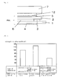
- the adhesive provided between the liquid crystal display panel PNL and the transparent cover 7 has a thickness of 0.05 mm to 0.1 mm in the conventional structure similar to that shown in FIG. 3 .
- the adhesive layer changes in form as a result of moisture absorption in a reliability test, which is performed in a high temperature high moisture environment, and furthermore, such a problem arises that the liquid crystal display panel changes form, thereby causing inconsistent display.
- the film thickness, which can prevent inconsistent display, is approximately 0.09 mm or greater.
- FIG. 8 is a graph showing the film thickness of the adhesive layer (mm) along the lateral axis and the ratio of the area where the display is inconsistent to the area of effective display in a liquid crystal display panel PNL along the longitudinal axis, and it can be seen from this that the film thickness of the adhesive layer which does not cause inconsistent display is approximately 0.09 mm or greater.
- approximately 0.1 mm is the limit of the thickness in the prior art, where an adhesive is used as described above, and it is difficult to make the film as thick as approximately 1 mm.
- viscous films it is easy to change the thickness of the viscous films by changing the thickness of application to a support body on which the film is formed during the manufacturing process, and viscous films having a thickness of approximately 1 mm are sold as products. It is possible to meet the thickness requirement of the connecting layer by using these viscous films.
- liquid crystal display panel PNL and a transparent cover 7 are attempted to be separated from each other forcibly by applying force, the liquid crystal display panel PNL or the transparent cover 7 is broken and becomes a defect because the adhesiveness of the adhesive film is as strong as approximately 100 N/cm2 immediately after being pasted. Therefore, liquid crystal display devices using a viscous film are disposed of as waste without being restored according to the prior art.
- current liquid display panels PNL have a thickness of approximately 0.2 mm in such a state that the first substrate 1 and the second substrate 2 are pasted via a sealing material 3 , and a problem arises in that they cannot be separated forcefully without being broken.
- the problems may arise not only with liquid crystal display devices using a liquid crystal display panel display, but also with other devices using a display panel of another type.
- An object of the present invention is to provide a display device where the display panel and the transparent cover, which are pasted together, can be separated without the liquid crystal display panel or the transparent cover being broken.
- the above described object can be achieved by an embodiment of the present invention which provides a display device where the viscous film for pasting the transparent cover to the display panel is a material where two layers of gluing agents are layered on top of each other.
- the above described object can also be achieved by another embodiment of the present invention which provides a display device where the viscous film for pasting the transparent cover to the display panel is a material where a gluing agent and a resin layer are layered on top of each other.
- the display device is, for example, a display device having: a liquid crystal display panel having a liquid crystal layer sandwiched between a first substrate and a second substrate which is provided on the viewer side relative to the first substrate; a polarizing plate provided on the above described liquid crystal display panel on the above described viewer side; a gluing agent pasted on the viewer side relative to the above described polarizing plate; and a transparent cover pasted on the viewer side relative to the above described gluing agent, and is characterized in that
- the above described gluing agent is made up of a multilayer body having a gluing agent pasted on the polarizing plate side and a gluing agent pasted on the transparent cover side.
- the display device is, for example, a display device having: a liquid crystal display panel having a liquid crystal layer sandwiched between a first substrate and a second substrate which is provided on the viewer side relative to the first substrate; a polarizing plate provided on the above described liquid crystal display panel on the above described viewer side; a viscous film pasted on the viewer side relative to the above described polarizing plate; and a transparent cover pasted on the viewer side relative to the above described viscous film, and is characterized in that
- the above described viscous film is made up of a multilayer body of gluing agents.
- the display device according to the present invention is, for example, characterized in that the above described viscous film is formed of two layers in (2).
- the display device is, for example, characterized in that the above described viscous film is made of a first gluing agent pasted to the above described polarizing plate and a second gluing agent pasted to the above described transparent cover, and the strength in the adhesion between the above described polarizing plate and the first gluing agent and the strength in the adhesion between the above described transparent cover and the second gluing agent are higher than the strength in the adhesion in the interface between layers of the above described first gluing agent and the above described second gluing agent in (2) or (3).
- the display device according to the present invention is, for example, characterized in that the above described first adhesive and the above described second adhesive are in such a state as to be separable between the above described first gluing agent and the above described second gluing agent in (4).
- the display device according to the present invention is, for example, characterized in that the thickness of the above described viscous film is in a range from 0.1 mm to 1 mm in any of (2), (3) and (4).
- the display device according to the present invention is, for example, characterized in that the above described viscous film has a transmittance of visible light of 90% or higher in any of (2), (3) and (4).
- the display device according to the present invention is, for example, characterized in that the materials of the above described first gluing agent and the above described second gluing agent which form the above described viscous film are acryl based oligomers or acryl based polymers in any of (2), (3) and (4).
- the display device according to the present invention is, for example, characterized in that the above described transparent cover functions as a touch panel in any of (1) to (8).
- the display device is, for example, a display device having: a liquid crystal display panel having a liquid crystal layer sandwiched between a first substrate and a second substrate which is provided on the viewer side relative to the above described first substrate; a polarizing plate provided on the above described liquid crystal display panel on the above described viewer side; a viscous film pasted on the viewer side relative to the above described polarizing plate; and a transparent cover pasted on the viewer side relative to the above described viscous film, and is characterized in that
- the above described viscous film is a multilayer material of a gluing agent and a resin layer.
- the display device according to the present invention is, for example, characterized in that the above described multilayer material is formed of three layers in (10).
- the display device according to the present invention is, for example, characterized in that the thickness of the above described viscous film is in a range from 0.1 mm to 1 mm in (10) or (11).
- the display device according to the present invention is, for example, characterized in that the above described viscous film has a transmittance of visible light of 90% or higher in any of (10) to (12).
- the display device according to the present invention is, for example, characterized in that the above described transparent cover functions as a touch panel in any of (10) to (13).
- the display device according to the present invention is, for example, characterized in that the material of the above described gluing agent which forms the above described viscous film is an acryl based oligomer or an acryl based polymer in any of (11) to (14).
- the material of the above described resin layer which forms the above described viscous film is made of polyethylene terephthalate or a cycloolefin polymer in any of (10) to (15).
- the manufacturing method for a display device is, for example, the manufacturing method for the display in any of (1) to (16), and characterized in that the above described transparent cover and the above described liquid crystal display panel are separated from each other and reused using a means for holding the above described display device flat while applying heat and a means for applying a load linearly from one side of the above described viscous film toward the other side.
- the display device according to the present invention is, for example, a display device characterized in that a gluing agent remains on the surface of the above described separated transparent cover and liquid crystal display panel in the manufacturing method in (17).
- Typical effects of the present invention are as follows.
- a multilayer adhesive material or viscous film is used to paste the display panel and the transparent cover together, and therefore, the weak gluing agents are separated from each other when an external force is applied, so that the display panel and the transparent cover can be separated.
- a viscous sheet where a gluing agent and a resin layer are layered on top of each other is used to paste a transparent cover to a display panel, and the gluing agent and the resin layer, which have weak adhesion, are separated when an external force is applied, so that the display panel and the transparent cover can be separated.
- FIG. 1 is a cross sectional diagram showing the display device according to the first embodiment of the present invention
- FIG. 2 is a perspective diagram showing the manner in which a display panel and a transparent cover are pasted together according of the present invention
- FIG. 3 is a cross sectional diagram showing the structure of a conventional display device
- FIG. 4 is a graph comparing the peel strength of various gluing agents
- FIG. 5 is a diagram schematically illustrating a method for separating the transparent cover and the liquid crystal display panel
- FIG. 6 is a graph showing the relationship between the temperature to which the gluing agent is heated and the strength in the adhesiveness of the gluing material
- FIG. 7 is a cross sectional diagram showing the display device according to the second embodiment of the present invention.
- FIG. 8 is a graph showing the relationship between the film thickness of the adhesive layer and inconsistency in the display.
- FIG. 1 is a cross sectional diagram showing the display device according to the first embodiment of the present invention.
- FIG. 2 is a perspective diagram showing the manner in which a display panel and a transparent cover are pasted together according to the present invention.
- FIG. 3 is a cross sectional diagram showing the structure of a conventional display device.
- FIG. 3 shows a case where a liquid crystal display panel is used as the display panel.
- the liquid crystal display panel PNL has an insulating and transparent first substrate 1 and second substrate 2 , which are formed of glass, for example.
- the first substrate 1 and the second substrate 2 are pasted together with a sealing material 3 in between.
- a liquid crystal layer 6 is sandwiched between the first substrate 1 and the second substrate 2 .
- the sealing material 3 is provided in a peripheral portion, outside the display region 13 in the liquid crystal display panel, and surrounds the liquid crystal layer 6 .
- the second substrate 2 side is the viewer side (front side) in the arrangement.
- the first substrate 1 and the second substrate 2 both have a thickness of 0.3 mm and the liquid crystal layer 6 has a thickness of 4 ⁇ m, the thickness is not limited to this.
- a number of independently driven pixels are arranged in a matrix in the display region 13 of the liquid crystal display panel PNL.
- a number of scan signal lines, a number of video signal lines which cross the number of scan signal lines, a number of switching elements made of thin film transistors, and a number of pixel electrodes are formed on the surface of the first substrate 1 on the liquid crystal layer 6 side.
- one or a number of counter electrodes are formed on the surface of the first substrate 1 or the second substrate 2 on the liquid crystal layer 6 side.
- the electrical field generated as a result of the difference in potential between the pixel electrodes and the counter electrode(s) drives the liquid crystal molecules in the liquid crystal layer 6 , so that an image is displayed in the display region 13 .
- the liquid crystal display panel has a polarizing plate 4 provided on the surface of the first substrate 1 on the side opposite to the liquid crystal layer 6 , and a polarizing plate 5 provided on the surface of the second substrate 2 on the side opposite to the liquid crystal layer 6 .
- the polarizing plate 4 and the polarizing plate 5 both have a thickness of 0.15 mm. However, the thickness is not limited to this.
- a transparent cover 7 is pasted to the surface of the liquid crystal display panel on the viewer side with a viscous film 12 in between.
- the viscous film 12 is pasted to the transparent cover 7 on the rear side, and then the transparent cover is pasted to the liquid crystal display panel.
- a material having little difference in the index of refraction with the transparent cover 7 (it is desirable for the difference in the index of refraction to be 0.2 or less), for example a gluing agent made of an acryl based oligomer or polymer, can be used for the viscous film 12 , so that it becomes possible to reduce unnecessary reflection in the interface.
- the transparent cover 7 is formed of a transparent material, such as glass or an acryl resin, and functions as a protective cover panel. It is desirable for the thickness to be 0.5 mm to 2.5 mm. In the present embodiment, for example, the thickness is 1.0 mm.
- the liquid crystal display panel has a region where the first substrate 1 sticks out from over the second substrate 2 on at least one side, and a drive circuit 14 formed of a semiconductor chip is mounted in this protruding region.
- a terminal for connection to the outside is formed in the protruding portion, so that a flexible wiring board 15 can be connected through this terminal.
- the structure is not limited to this, and the location of the end portion of the first substrate and the end portion of the second substrate 2 may be approximately the same along the sides other than the side along which the drive circuit 14 or flexible wiring board 15 is mounted. This is the same in the other embodiments.
- the viscous film 12 has a strength of as high as approximately 100 N/cm2 in adhesion immediately after the transparent cover 7 and the liquid crystal display panel are pasted together. Therefore, when the transparent cover 7 is separated from a defective liquid crystal display panel during the manufacturing process in order to be restored and reused, a problem may arise, such that the liquid crystal display panel or the transparent cover 7 breaks, if the liquid crystal display panel and the transparent cover are forcefully separated by applying a force.
- the embodiment of the present invention is characterized in that the viscous film for pasting the transparent cover 7 and the liquid crystal display panel together is a multilayer viscous film made up of a first gluing agent 8 pasted on the liquid crystal display panel PNL side and a second gluing agent 9 pasted on the transparent cover 7 side.
- FIG. 4 is a graph showing the results of examination of the strength in adhesion through peeling tests in the case where the adhesive film between the transparent cover 7 and the liquid crystal display panel PNL is a single layer viscous film (viscous film A, viscous film B) and the multilayer viscous film of the present embodiment.
- the strength in adhesion between the two is approximately 100 N/cm2. In the case where the transparent cover 7 (substrate A) and the liquid crystal display panel PNL (substrate B) are pasted together with a viscous film B pasted on the substrate A side, the strength in adhesion between the two is approximately 110 N/cm2.
- the strength in adhesion between the two is approximately 75 N/cm2.
- adhesives are flexible solids having a rubber hardness of approximately 10, and thus, the adhesiveness increases when they are pressed against the object to which it is to adhere and the area of contact increases. Accordingly, in the case where they are pasted to a rigid body, such as a transparent cover 7 or a liquid crystal display panel PNL, they are pressed sufficiently for the area of adhesion to increase, and they are pasted with high strength in adhesion.
- a rigid body such as a transparent cover 7 or a liquid crystal display panel PNL
- they are pasted with high strength in adhesion.
- adhesives are layered on top of each other, they are not sufficiently pressed against each other, even when they make contact with each other, because they are both flexible materials, and thus, the area for adhesion does not increase, and the strength in adhesion cannot be considered to increase.
- multilayer viscous films have such effects as to make separation of the transparent cover 7 and the liquid crystal display panel PNL easy.
- FIG. 5 which corresponds to FIG. 1
- a linear load 11 of a thread made of nylon or a polyvinylidene fluoride resin applies an external force from one side of the multilayer viscous film toward the other side, so that the first gluing agent 8 and the second gluing agent 9 peel from each other, and thus, the transparent cover 7 and the liquid crystal display panel PNL are separated from each other.
- nylon thread is used for the linear load 11
- the diameter of the linear load 11 is approximately 0.05 mm to 1.0 mm (preferably 0.2 mm).
- FIG. 6 is a graph showing the dependency of the strength in adhesion when the viscous films are heated, and the lateral axis is the temperature to which the viscous films are heated (° C.), while the longitudinal axis is the strength in adhesion (N/cm2).
- the temperature at the time of separation is determined by the heatproof temperature of the respective members of the transparent cover 7 and the liquid crystal display panel PNL, and it is desirable for it to be in a range from 50° C. to 80° C. (preferably 70° C.).
- the heating means it is desirable to use a hot plate, an infrared ray heater or a hot air circulating oven, for example.
- FIG. 7 is a cross sectional diagram showing the display device according to the second embodiment of the present invention, and corresponds to FIG. 1 .
- FIG. 7 is different from that in FIG. 1 in that a multilayer viscous film where a gluing agent 10 made of an acryl based oligomer or polymer between a viscous film 9 made of polyethylene terephthalate or a cycloolefin polymer provided on the surface of the transparent cover 7 on the liquid crystal panel PNL side, and a viscous film 8 provided on the surface of the liquid crystal panel PNL on the transparent cover 7 side is provided.
- a gluing agent 10 made of an acryl based oligomer or polymer between a viscous film 9 made of polyethylene terephthalate or a cycloolefin polymer provided on the surface of the transparent cover 7 on the liquid crystal panel PNL side
- a viscous film 8 provided on the surface of the liquid crystal panel PNL on the transparent cover 7 side
- the gluing agent 10 in this multilayer viscous film is applied on the two surfaces of the resin layers, and the strength in adhesion can be made weak.
- the viscous film in which the gluing agent 10 and the resin layers are layered has such effects that the transparent cover 7 and the liquid crystal display panel PNL are easy to separate from each other.
- the transparent cover 7 and the liquid crystal display panel PNL in the display device shown in FIG. 7 are separated under the same conditions as in the first embodiment, they can be separated from each other without damaging the transparent cover 7 and the liquid crystal display panel, as in the first embodiment.
Abstract
Description
- [Patent Document 1] Japanese Unexamined Patent Publication 2007-178758
(5) The display device according to the present invention is, for example, characterized in that the above described first adhesive and the above described second adhesive are in such a state as to be separable between the above described first gluing agent and the above described second gluing agent in (4).
(6) The display device according to the present invention is, for example, characterized in that the thickness of the above described viscous film is in a range from 0.1 mm to 1 mm in any of (2), (3) and (4).
(7) The display device according to the present invention is, for example, characterized in that the above described viscous film has a transmittance of visible light of 90% or higher in any of (2), (3) and (4).
(8) The display device according to the present invention is, for example, characterized in that the materials of the above described first gluing agent and the above described second gluing agent which form the above described viscous film are acryl based oligomers or acryl based polymers in any of (2), (3) and (4).
(9) The display device according to the present invention is, for example, characterized in that the above described transparent cover functions as a touch panel in any of (1) to (8).
(10) The display device according to the present invention is, for example, a display device having: a liquid crystal display panel having a liquid crystal layer sandwiched between a first substrate and a second substrate which is provided on the viewer side relative to the above described first substrate; a polarizing plate provided on the above described liquid crystal display panel on the above described viewer side; a viscous film pasted on the viewer side relative to the above described polarizing plate; and a transparent cover pasted on the viewer side relative to the above described viscous film, and is characterized in that
(16) The display device according to the present invention is, for example, characterized in that the material of the above described resin layer which forms the above described viscous film is made of polyethylene terephthalate or a cycloolefin polymer in any of (10) to (15).
(17) The manufacturing method for a display device according to the present invention is, for example, the manufacturing method for the display in any of (1) to (16), and characterized in that the above described transparent cover and the above described liquid crystal display panel are separated from each other and reused using a means for holding the above described display device flat while applying heat and a means for applying a load linearly from one side of the above described viscous film toward the other side.
(18) The display device according to the present invention is, for example, a display device characterized in that a gluing agent remains on the surface of the above described separated transparent cover and liquid crystal display panel in the manufacturing method in (17).
Claims (14)
Applications Claiming Priority (2)
| Application Number | Priority Date | Filing Date | Title |
|---|---|---|---|
| JP2008165263A JP5142854B2 (en) | 2008-06-25 | 2008-06-25 | Display device and manufacturing method thereof |
| JP2008-165263 | 2008-06-25 |
Publications (2)
| Publication Number | Publication Date |
|---|---|
| US20090322999A1 US20090322999A1 (en) | 2009-12-31 |
| US8212972B2 true US8212972B2 (en) | 2012-07-03 |
Family
ID=41446967
Family Applications (1)
| Application Number | Title | Priority Date | Filing Date |
|---|---|---|---|
| US12/490,522 Active 2030-08-07 US8212972B2 (en) | 2008-06-25 | 2009-06-24 | Display device with multilayer body having at least one layer of a gluing agent |
Country Status (2)
| Country | Link |
|---|---|
| US (1) | US8212972B2 (en) |
| JP (1) | JP5142854B2 (en) |
Families Citing this family (7)
| Publication number | Priority date | Publication date | Assignee | Title |
|---|---|---|---|---|
| WO2012087804A1 (en) * | 2010-12-21 | 2012-06-28 | 3M Innovative Properties Company | Articles having optical adhesives and method of making same |
| DE102012224352A1 (en) * | 2012-12-21 | 2014-06-26 | Continental Automotive Gmbh | Electro-optical display with a transparent cover |
| CN105026136B (en) * | 2013-03-21 | 2016-11-30 | 夏普株式会社 | The manufacture method of panel layer stack and solid state method of discrimination |
| KR102174761B1 (en) * | 2013-08-14 | 2020-11-06 | 삼성디스플레이 주식회사 | Flexible display device and method for fabricating the same |
| CN104199206B (en) | 2014-08-19 | 2017-10-27 | 京东方光科技有限公司 | A kind of display device and its assembly method |
| JP6870164B2 (en) * | 2016-06-03 | 2021-05-12 | 天馬微電子有限公司 | Display device and manufacturing method of display device |
| EP3785897B1 (en) | 2019-08-29 | 2021-12-29 | SHPP Global Technologies B.V. | Transparent, flexible, impact resistant, multilayer film comprising polycarbonate copolymers |
Citations (10)
| Publication number | Priority date | Publication date | Assignee | Title |
|---|---|---|---|---|
| US5880800A (en) * | 1996-01-09 | 1999-03-09 | Nitto Denko Corporation | Optical film and liquid crystal display |
| US20030098931A1 (en) * | 2000-06-01 | 2003-05-29 | Yuuji Saiki | Optical member and liquid crystal display device |
| JP2004240455A (en) | 1998-01-09 | 2004-08-26 | Nissha Printing Co Ltd | Liquid crystal display device of touch input method |
| JP2004354557A (en) | 2003-05-28 | 2004-12-16 | Nitto Denko Corp | Polarizing plate, optical film and image display |
| JP2005017704A (en) | 2003-06-26 | 2005-01-20 | Nitto Denko Corp | Polarizing plate and its manufacturing method, polarizing plate protective film, optical film using polarizing plate, and image display device |
| JP2005189571A (en) | 2003-12-26 | 2005-07-14 | Nitto Denko Corp | Laminated sheet and image display device |
| US20060082708A1 (en) * | 2004-10-19 | 2006-04-20 | Nitto Denko Corporation | Polarizing plate, method of producing a polarizing plate, and liquid crystal panel, liquid crystal television, and liquid crystal display apparatus all using the same |
| JP2007178758A (en) | 2005-12-28 | 2007-07-12 | Seiko Instruments Inc | Display device |
| JP2008116788A (en) | 2006-11-07 | 2008-05-22 | Fujifilm Corp | Polarizing plate and image display device |
| JP2008158251A (en) | 2006-12-25 | 2008-07-10 | Hitachi Displays Ltd | Manufacturing method of display device |
Family Cites Families (5)
| Publication number | Priority date | Publication date | Assignee | Title |
|---|---|---|---|---|
| JP3220403B2 (en) * | 1996-02-09 | 2001-10-22 | セイコーインスツルメンツ株式会社 | Display device manufacturing method |
| JP3710368B2 (en) * | 2000-09-25 | 2005-10-26 | シャープ株式会社 | Manufacturing method of laminated film |
| JP2003177241A (en) * | 2001-12-10 | 2003-06-27 | Fujimori Kogyo Co Ltd | Laminated body for optical use, adhesive transfer tape and method for manufacturing laminated body for optical use |
| JP2005173462A (en) * | 2003-12-15 | 2005-06-30 | Nitto Denko Corp | Glass crack prevention laminate and liquid crystal display |
| JP5162908B2 (en) * | 2006-05-26 | 2013-03-13 | 住友化学株式会社 | Optical laminate having polarizing film with adhesive and set of polarizing film |
-
2008
- 2008-06-25 JP JP2008165263A patent/JP5142854B2/en active Active
-
2009
- 2009-06-24 US US12/490,522 patent/US8212972B2/en active Active
Patent Citations (10)
| Publication number | Priority date | Publication date | Assignee | Title |
|---|---|---|---|---|
| US5880800A (en) * | 1996-01-09 | 1999-03-09 | Nitto Denko Corporation | Optical film and liquid crystal display |
| JP2004240455A (en) | 1998-01-09 | 2004-08-26 | Nissha Printing Co Ltd | Liquid crystal display device of touch input method |
| US20030098931A1 (en) * | 2000-06-01 | 2003-05-29 | Yuuji Saiki | Optical member and liquid crystal display device |
| JP2004354557A (en) | 2003-05-28 | 2004-12-16 | Nitto Denko Corp | Polarizing plate, optical film and image display |
| JP2005017704A (en) | 2003-06-26 | 2005-01-20 | Nitto Denko Corp | Polarizing plate and its manufacturing method, polarizing plate protective film, optical film using polarizing plate, and image display device |
| JP2005189571A (en) | 2003-12-26 | 2005-07-14 | Nitto Denko Corp | Laminated sheet and image display device |
| US20060082708A1 (en) * | 2004-10-19 | 2006-04-20 | Nitto Denko Corporation | Polarizing plate, method of producing a polarizing plate, and liquid crystal panel, liquid crystal television, and liquid crystal display apparatus all using the same |
| JP2007178758A (en) | 2005-12-28 | 2007-07-12 | Seiko Instruments Inc | Display device |
| JP2008116788A (en) | 2006-11-07 | 2008-05-22 | Fujifilm Corp | Polarizing plate and image display device |
| JP2008158251A (en) | 2006-12-25 | 2008-07-10 | Hitachi Displays Ltd | Manufacturing method of display device |
Also Published As
| Publication number | Publication date |
|---|---|
| JP2010008525A (en) | 2010-01-14 |
| JP5142854B2 (en) | 2013-02-13 |
| US20090322999A1 (en) | 2009-12-31 |
Similar Documents
| Publication | Publication Date | Title |
|---|---|---|
| US8212972B2 (en) | Display device with multilayer body having at least one layer of a gluing agent | |
| US8279391B2 (en) | Liquid crystal display device with grounded by thermocompression bonding tape and double-side adhesive tape | |
| US8319709B2 (en) | Display device and manufacturing method thereof | |
| TWI282879B (en) | Liquid crystal display device | |
| US6914640B2 (en) | Touch panel liquid crystal display device and method of fabricating the same | |
| US10455693B2 (en) | Display device comprising remaining portion of inspection line with cut edge | |
| US20140226111A1 (en) | Method for manufacturing curved-surface display | |
| KR101247680B1 (en) | Electrophoretic Display Device and Method for Manufacturing thereof | |
| JP2011022220A (en) | Protection-plate-attached electronic member | |
| JP5347068B2 (en) | Manufacturing method of display device | |
| US8471985B2 (en) | Liquid crystal display panel | |
| CN1274996A (en) | Anti-dazzle touch plate | |
| JP2008009225A (en) | Display device and its manufacturing method | |
| US20210011332A1 (en) | Display device and method of manufacturing the same | |
| JPH10186397A (en) | Liquid crystal display device and its production | |
| JP2007310344A (en) | Polarizing plate and liquid crystal display using the same | |
| US8059225B2 (en) | V-shaped pallet comprising a main pallet and an auxiliary pallet having first and second plane sections jointed in a V-shape configured for a liquid crystal display panel | |
| JP2008209695A (en) | Electrophoresis display device and its manufacturing method | |
| KR102108842B1 (en) | Touch Panel | |
| JP2008185870A (en) | Electro-optical device, method for manufacturing the same, and electronic equipment | |
| JP2020134848A (en) | Liquid crystal display device | |
| JP2002258757A (en) | Display element, method for protecting surface of the same, method for producing the same, method for producing liquid crystal device and electronic appliance | |
| US20210373367A1 (en) | Display apparatus | |
| KR101363341B1 (en) | Electrophoretic Display Device and Method for Manufacturing thereof | |
| JP2007010706A (en) | Liquid crystal device and method for manufacturing the same |
Legal Events
| Date | Code | Title | Description |
|---|---|---|---|
| AS | Assignment |
Owner name: HITACHI DISPLAYS, LTD., JAPAN Free format text: ASSIGNMENT OF ASSIGNORS INTEREST;ASSIGNORS:SANO, YASUSHI;SENTOU, KIYOSHI;NAKATSUKA, HIDEAKI;AND OTHERS;REEL/FRAME:023052/0717;SIGNING DATES FROM 20090615 TO 20090712 Owner name: HITACHI DISPLAYS, LTD., JAPAN Free format text: ASSIGNMENT OF ASSIGNORS INTEREST;ASSIGNORS:SANO, YASUSHI;SENTOU, KIYOSHI;NAKATSUKA, HIDEAKI;AND OTHERS;SIGNING DATES FROM 20090615 TO 20090712;REEL/FRAME:023052/0717 |
|
| AS | Assignment |
Owner name: IPS ALPHA SUPPORT CO., LTD., JAPAN Free format text: COMPANY SPLIT PLAN TRANSFERRING FIFTY (50) PERCENT SHARE IN PATENT APPLICATIONS;ASSIGNOR:HITACHI DISPLAYS, LTD.;REEL/FRAME:027092/0684 Effective date: 20100630 Owner name: PANASONIC LIQUID CRYSTAL DISPLAY CO., LTD., JAPAN Free format text: MERGER;ASSIGNOR:IPS ALPHA SUPPORT CO., LTD.;REEL/FRAME:027093/0937 Effective date: 20101001 |
|
| STCF | Information on status: patent grant |
Free format text: PATENTED CASE |
|
| FEPP | Fee payment procedure |
Free format text: PAYOR NUMBER ASSIGNED (ORIGINAL EVENT CODE: ASPN); ENTITY STATUS OF PATENT OWNER: LARGE ENTITY |
|
| FPAY | Fee payment |
Year of fee payment: 4 |
|
| MAFP | Maintenance fee payment |
Free format text: PAYMENT OF MAINTENANCE FEE, 8TH YEAR, LARGE ENTITY (ORIGINAL EVENT CODE: M1552); ENTITY STATUS OF PATENT OWNER: LARGE ENTITY Year of fee payment: 8 |
|
| AS | Assignment |
Owner name: JAPAN DISPLAY, INC., JAPAN Free format text: CHANGE OF ADDRESS;ASSIGNOR:JAPAN DISPLAY, INC.;REEL/FRAME:065654/0250 Effective date: 20130417 Owner name: PANASONIC INTELLECTUAL PROPERTY CORPORATION OF AMERICA, CALIFORNIA Free format text: NUNC PRO TUNC ASSIGNMENT;ASSIGNOR:PANASONIC LIQUID CRYSTAL DISPLAY CO., LTD.;REEL/FRAME:065615/0327 Effective date: 20230828 Owner name: JAPAN DISPLAY, INC., JAPAN Free format text: CHANGE OF NAME;ASSIGNOR:JAPAN DISPLAY EAST, INC.;REEL/FRAME:065614/0644 Effective date: 20130401 Owner name: JAPAN DISPLAY EAST, INC., JAPAN Free format text: CHANGE OF NAME;ASSIGNOR:HITACHI DISPLAYS, LTD.;REEL/FRAME:065614/0223 Effective date: 20120401 |
|
| MAFP | Maintenance fee payment |
Free format text: PAYMENT OF MAINTENANCE FEE, 12TH YEAR, LARGE ENTITY (ORIGINAL EVENT CODE: M1553); ENTITY STATUS OF PATENT OWNER: LARGE ENTITY Year of fee payment: 12 |