BACKGROUND
Some electronic circuits impose an upper limit on a current that may be delivered to a load with the purpose of protecting the circuit or the load. For example, a universal serial bus (USB) has an upper current limit of 100 mA when it operates in a low power mode, and has an upper current limit of 500 mA when it operates in a high power mode.
FIG. 1 illustrates a conventional current limit circuit 100. The current limit circuit 100 includes a controller 116, a converter 120, and a switch 110, such as a metal oxide semiconductor field effect transistor (MOSFET). An input power source VIN is coupled to a load 102 through an output node VSYS via the switch 110. The controller 116 is coupled to the switch 110 and the output node VSYS to monitor a voltage at the output node VSYS. The input power source VIN is also coupled to a battery 104 at the node VSYS to charge the battery 104. A current flowing through the switch 110 can increase as a power demand of the load 102 increases. By monitoring the voltage at the output node VSYS, once the current flowing through the switch 110 reaches a predetermined upper current limit, the switch 110 operates in a linear mode to limit the current flowing through the switch 110. If the power demand of the load 102 keeps increasing, the input power source VIN alone may not provide sufficient power to the load 102. Consequently, the converter 120 can provide extra power from the battery 104 to the load 102.
However, by operating the switch 110 in the linear mode, it causes a thermal problem and extra power consumption.
SUMMARY
A system includes a power bus and a circuit. The power bus delivers power from a first power source to an output node. The circuit monitors a current flowing through the power bus and provides power from a second power source to the output node based on an amount of the current, and maintains a voltage level of the output node in a predetermined range.
BRIEF DESCRIPTION OF THE DRAWINGS
Features and advantages of embodiments of the claimed subject matter will become apparent as the following detailed description proceeds, and upon reference to the drawings, wherein like numerals depict like parts, and in which:
FIG. 1 shows a diagram of a conventional current limit circuit.
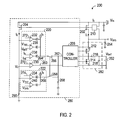
FIG. 2 shows a diagram of a current limit circuit, in accordance with one embodiment of the present invention.
FIG. 3 shows a flowchart of a method for powering a load, in accordance with one embodiment of the present invention.
DETAILED DESCRIPTION
Reference will now be made in detail to the embodiments of the present invention. While the invention will be described in conjunction with these embodiments, it will be understood that they are not intended to limit the invention to these embodiments. On the contrary, the invention is intended to cover alternatives, modifications and equivalents, which may be included within the spirit and scope of the invention as defined by the appended claims.
Furthermore, in the following detailed description of the present invention, numerous specific details are set forth in order to provide a thorough understanding of the present invention. However, it will be recognized by one of ordinary skill in the art that the present invention may be practiced without these specific details. In other instances, well known methods, procedures, components, and circuits have not been described in detail as not to unnecessarily obscure aspects of the present invention.
According to one embodiment of present invention, a system includes a first power source and a second power source. The first power source and the second power source are operable for powering a load coupled at an output node of the system. The system can control the current from the first power source to the load within a predetermined range, e.g., below an upper current limit. The system can also maintain a voltage at the output node within a predetermined range. Advantageously, instead of operating a switch in the linear mode to limit the current, the system provides power from a second power source to the load when the current from the first power source exceeds a threshold. In other words, the first power source and the second power source power the load simultaneously when the current from the power source exceeds the threshold. Moreover, the system can adjust power from the second power source according to the current from the first power source. Thus, the current from the first power source can be maintained below the upper current limit. As such, power consumption and the thermal problem caused by the switch working in the linear mode can be avoided.
FIG. 2 shows a diagram of a current limit circuit 200, in accordance with one embodiment of the present invention. The current limit circuit 200 includes a first power source, e.g., a power source VIN, and a second power source, e.g., a battery 252. The power source VIN and the battery 252 can power the load 254. In one embodiment, either the power source VIN or the battery 252 powers the load 254. In another embodiment, both power source VIN and battery 252 can power the load 254 simultaneously. In one embodiment, the power source VIN can charge the battery 254.
A power bus including a switch 202, is used to deliver power from the power source VIN to an output node VSYS. In one embodiment, the load 254 is coupled to the output node VSYS. The current I1 flowing through the switch 202 can vary in accordance with the power demand of the load 254. For example, if the power demand of the load 254 increases, the current I1 can be increased accordingly in order to satisfy the power demand of the load 254.
The current limit circuit 200 can monitor the current I1 flowing through the switch 202. The current limit circuit 200 is operable for providing power from the battery 252, to the output node VSYS based on the amount of the current I1, e.g., when the current I1 reaches or exceeds a predetermined threshold. By providing an extra current from the battery 252 to the load 254, the current I1 flowing through the switch 202 can be maintained below a predetermined threshold.
In one embodiment, the current limit circuit 200 includes a current control block 280 and a converter 282. The current control block 280 coupled to the switch 202 and the output node Vsys monitors the current I1 flowing through the switch 202 and compares the current I1 with a first threshold 270. The current control block 280 controls the converter 282. The converter 282 can selectively operate in a first mode or a second mode. In the first mode, the converter 282 receives power from the power source VIN and generates proper power to charge the battery 252. In the second mode, the converter 282 provides power from the battery 252 to the load 254 via the output node Vsys. Advantageously, the converter 282 operates in the second mode when the current I1 reaches or exceeds the first threshold 270, in one embodiment. Thus, in the second mode, both power source VIN and battery 252 power the load 254 simultaneously. As a result, the current I1 can be maintained below an upper current limit.
Moreover, the voltage level of the output node VSYS can be maintained in a predetermined range. The switch 202 performs in the normal switch mode (fully on or fully off) instead of the linear mode. Hence, the thermal problem and the extra power consumption caused by the switch 110 in the conventional current limit circuit 100 can be avoided.
In one embodiment, the switch 202 is a p-channel MOSFET, and a selector 210 compares the voltage levels between the power source VIN and the output node VSYS and applies a higher voltage to the bulk of the p-MOSFET 202.
In one embodiment, the current control block 280 includes a switch 204, a comparator 230, control blocks 220 and 222, and a controller 206. In one embodiment, the switch 204 and the switch 202 form a current mirror. The current I2 flowing through the switch 204 is proportional to the current I1 flowing through the switch 202. Furthermore, a resistor 290 converts the current I2 to a voltage V2 indicative of the current I1.
The comparator 230 can be used to compare the voltage signal V2 with the first threshold 270 and output a mode signal 260 to selectively enable the first control block 220 or the second control block 222 to control the converter 282. More specifically, the mode signal 260 turns on a switch 286 to enable the control block 220 or turns on a switch 288 to enable the control block 222. In one embodiment, the control block 220 is enabled to control the converter 282 in the first mode, and the second control block 222 is enabled to control the converter 282 in the second mode.
In one embodiment, when the voltage V2 is less than the first threshold 270, the switch 286 is switched on. Thus, the control block 220 is enabled based on the mode signal 260. As such, the converter 282 in the first mode receives the power from the power source VIN and generates proper power to charge the battery 252.
In one embodiment, when the voltage V2 is greater than the first threshold 270, the switch 288 is switched on. Thus, the control block 222 is enabled based on the mode signal 260. As such, the converter 282 in the second mode provides the power from the battery 252 to the load 254 via the output node VSYS.
In one embodiment, when the control block 220 is enabled, a resistor 268 converts a current signal 264 generated by the control block 220 to a control signal 262 to control the converter 282. The mode signal 260 controls the converter 282 to operate in the first mode. In the first mode, the power source VIN charges the battery 252. Meanwhile, the power source VIN can also power the load 254.
In one embodiment, the control block 220 includes an amplifier, such as an operational transconductance amplifier (OTA) 232. The OTA 232 compares the voltage V2 with a threshold 272, and controls an amount of the power from the power source VIN to the battery 252 based on the voltage V2 and the threshold 272. The OTA 232 is coupled to a current source IS. In one embodiment, the threshold 272 is less than the first threshold 270.
When the voltage V2 indicative of the current I1 is less than the threshold 272, the control block 220 is enabled since the voltage V2 is less than the first threshold 270. In this instance, the output of the OTA 232 does not affect the current signal 264.
When the power demand of the load 254 increases, the voltage V2 indicative of the current I1 increases accordingly. When the voltage V2 is greater than the threshold 272 but less than the first threshold 270, the current signal 264 varies according to a difference between the voltage V2 and the threshold 272. In other words, the OTA 232 sinks current from the current source IS when the voltage V2 is greater than the threshold 272. Therefore, the current signal 264 indicates an amount that the voltage V2 exceeds the threshold 272. In one embodiment, the higher the voltage V2, the less the current signal 264 will be. Thus, the amount of the power from the power source VIN to the battery 252 can be controlled based on the difference between the voltage V2 and the threshold 272 when the voltage V2 is greater than the threshold 272 but less than the first threshold 270.
In one embodiment, the control block 220 further includes a second amplifier 236 that compares the battery voltage VBAT to a voltage threshold VTH1. When the battery voltage VBAT is less than the voltage threshold VTH1, the output of the amplifier 236 does not affect the current signal 264. When the voltage VBAT is greater than the voltage threshold VTH1, the current signal 264 varies according to a difference between the voltage VBAT and the voltage threshold VTH1. In other words, the amplifier 236 sinks current from the current source IS when the voltage VBAT is greater than the voltage threshold VTH1. Thus, the amount of the power from the power source VIN to the battery 252 can be controlled based on the difference between the battery voltage VBAT and the voltage threshold VTH1 when the battery voltage VBAT exceeds the voltage threshold VTH1, in one embodiment.
In one embodiment, the control block 220 further includes a third amplifier 238 that compares a signal IA indicative of a current I3 from the power source VIN with a current threshold ITH. When the signal IA is less than the current threshold ITH, the output of the amplifier 238 does not affect the current signal 264. When the signal IA is greater than the current threshold ITH, the current signal 264 varies according to a difference between the signal IA and the current threshold ITH. In other words, the amplifier 238 sinks current from the current source Is when the signal IA is greater than the current threshold ITH. Thus, the amount of the power from the power source VIN to the battery 252 can be controlled based on the difference between the current IA and the threshold ITH when the signal IA is greater than the current threshold ITH, in one embodiment.
In one embodiment, the outputs of the OTA 232, the second amplifier 236 and the third amplifier 238 are coupled to a common node. The current signal 264 is generated based on the outputs of the OTA 232, the second amplifier 236, and the third amplifier 238. In one embodiment, the current signal 264 is determined by an output of the OTA 234, or output of the amplifier 236, or output of the amplifier 238, whichever is first generated.
In the first mode, the control signal 262 varies corresponding to the current signal 264. In one embodiment, when the power demand of the load 254 increases and the current I1 increases accordingly, the controller 206 controls the converter 282 to decrease an amount of the power delivered from the power source VIN to the battery 252, based on the control signal 262.
In one embodiment, if the current I1 keeps increasing and reaches the first threshold 270, the current signal 264 is decreased to substantially zero. The converter 282 stops delivering power from the power source VIN to the battery 252 based on the control signal 262, in one embodiment. As described above, when the current I1 is greater than the first threshold 270, the control block 220 is disabled and the control block 222 is enabled.
In one embodiment, when the control block 222 is enabled, the resistor 268 converts a current signal 266 generated by the control block 222 to the control signal 262 to control the converter 282. The mode signal 260 controls the converter 282 to operate in the second mode. In the second mode, the battery 252 powers the load 254. Meanwhile, the power source VIN can also power the load 254.
In one embodiment, the control block 222 includes an amplifier, such as an OTA 234. The OTA 234 compares the voltage V2 with a threshold 274 and controls an amount of the power provided by the battery 252 to the load 254 based on the voltage V2 and the threshold 274. Similar to the OTA 232, the OTA 234 is coupled to the current source Is. In one embodiment, the threshold 274 is greater than the first threshold 270.
When the voltage V2 indicative of the current I1 is greater than the first threshold 270, the control block 222 is enabled. In this instance, the controller 206 controls the converter 282 to provide the power from the battery 252 to the load 254. Meanwhile, the power source VIN also provides power to the load 254. By providing the extra current from the battery 252, the current I1 flowing through the switch 202 can be maintained below the predetermined threshold.
Similarly, the current signal 264 and the control signal 262 can vary according to a difference between the voltage V2 and the threshold 274. In one embodiment, the higher the voltage V2, the larger the current signal 266 will be. Consequently, the amount of power provided from the battery 252 to the load 254 is adjusted through the converter 282 based on the difference between the voltage V2 and the threshold 274 when the voltage V2 is less than the threshold 274 but greater than the first threshold 270.
In one embodiment, the control block further includes a fourth amplifier 240 that compares a voltage of output node VSYS to a voltage threshold VTH2. When the voltage of output node VSYS is greater than the voltage threshold VTH2, the output of the fourth amplifier 240 does not affect the current signal 266. When the voltage of output node VSYS is less than the voltage threshold VTH2, the current signal 266 varies according to a difference between the voltage of output node VSYS and the voltage threshold VTH2. In other words, the fourth amplifier 240 sinks current from the current source IS when the voltage of output node VSYS is less than the voltage threshold VTH2. Thus, the amount of the power from the power source VIN to the battery 252 can be controlled based on the difference between the voltage of output node VSYS and the voltage threshold VTH2 when the voltage of output node VSYS is less than the voltage threshold VTH2, in one embodiment.
In one embodiment, the outputs of the OTA 234 and the fourth amplifier 240 are coupled to a common node. The current signal 266 is generated based on the outputs of the OTA 234 and the fourth amplifier 240. In one embodiment, the current signal 266 is determined by an output of the OTA 234 or output of the amplifier 240, whichever is first generated.
In one embodiment, the converter 282 includes converter switches 212 and 214, an inductor 216, and a capacitor 218. The converter switch 212 is coupled to the switch 202 and the output node VSYS, and the converter switch 214 is coupled to the converter switch 212. The converter switches 212 and 214 are controlled by the controller 206 to operate in the first mode or the second mode. More specifically, the converter switches 212 and 214 converts between a first voltage level of the power source VIN, e.g., the voltage of the power source VIN, and a second voltage level of the battery 252, e.g., the battery voltage VBAT.
In the first mode, the mode signal 260 enables the control block 220, and the controller 206 receives the control signal 262 to control the converter 282 to deliver power from the power source VIN to the battery 252. More specifically, the controller 206 enables the converter switches 212 and 214 alternately to convert the voltage at the output node VSYS to a battery charging voltage VBAT.
In one embodiment, the converter 282 operates as a charger (e.g., a buck converter) in the first mode. As such, when the controller 206 enables the switch 212 and disables the switch 214, the power source VIN stores energy in the inductor 216 and charges the battery 252. When the controller 206 disables the switch 212 and enables the switch 214, the energy stored in the inductor 216 continues to provide charging current to the battery 252. As such, a step-down voltage is generated to charge the battery 252.
Similarly, In the second mode, the mode signal 260 enables the control block 222, and the controller 206 receives the control signal 262 to control the converter 282 to provide power from the battery 252 to the load 254. More specifically, the controller 206 enables the converter switches 212 and 214 alternately to convert the battery voltage VBAT to a voltage at the output node VSYS.
In one embodiment, the converter 282 operates as a boost converter in the second mode. When the controller 206 disables the converter switch 212 and enables the converter switch 214, the battery 252 stores energy in the inductor 216. When the controller 206 enables the converter switch 212 and disables the converter switch 214, the energy stored in the inductor 216 is provided to the load 254 via the output node VSYS. As such, a step-up voltage at the output node VSYS is generated to power the load 254. In an alternative embodiment, the converter 282 operates as a buck converter in the second mode to provide a step-down voltage at the output node VSYS to power the load 254.
As such, the converter switches 212 and 214 can be used to convert the voltage from the power source VIN to a battery charging voltage to charge the battery 252 or convert the battery voltage VBAT to a proper voltage to power the load 254. In one embodiment, the controller 206 controls the converter switches 212 and 214 by a pulse width modulation signal based on the control signal 262.
FIG. 3 is a flowchart 300 of a method for powering a load. Although specific steps are disclosed in FIG. 3, such steps are exemplary. That is, the present invention is well suited to performing various other steps or variations of the steps recited in FIG. 3. FIG. 3 is described in combination with FIG. 2.
In block 310, a voltage V2 indicative of a current I1 delivered from a power source VIN to a load 254 is compared with a threshold 270.
In block 320, the converter 282 operates in a first mode when the voltage V2 is less than the first threshold 270. In the first mode, the power source VIN provides power to charge a second power source, e.g., a battery 252. In one embodiment, the voltage V2 is compared to a threshold 272 in the first mode, and an amount of the power provided from the power source VIN to the battery 252 is decreased when the voltage V2 is greater than the threshold 272. Converter switches 212 and 214 can be controlled to adjust the amount of the power provided from the power source VIN to the battery 252, in one embodiment.
In block 330, the converter operates in a second mode when the voltage V2 is greater than the first threshold 270. In the second mode, the battery 252 provides power to the load 254. In one embodiment, the voltage V2 is compared to a threshold 274 in the second mode, and an amount of the power provided from the battery 252 to the load 254 is increased when the voltage V2 is greater than the threshold 274. Converter switches 212 and 214 can be controlled to adjust the amount of the power provided from the battery 252 to the load 254, in one embodiment. As the battery 252 also provides power to the load 254 in the second mode, the current I1 delivered from a power source VIN to a load 254 can be maintained below an upper current limit.
While the foregoing description and drawings represent embodiments of the present invention, it will be understood that various additions, modifications and substitutions may be made therein without departing from the spirit and scope of the principles of the present invention as defined in the accompanying claims. One skilled in the art will appreciate that the invention may be used with many modifications of form, structure, arrangement, proportions, materials, elements, and components and otherwise, used in the practice of the invention, which are particularly adapted to specific environments and operative requirements without departing from the principles of the present invention. The presently disclosed embodiments are therefore to be considered in all respects as illustrative and not restrictive, the scope of the invention being indicated by the appended claims and their legal equivalents, and not limited to the foregoing description.