US8222662B2 - LED package structure - Google Patents
LED package structure Download PDFInfo
- Publication number
- US8222662B2 US8222662B2 US12/975,232 US97523210A US8222662B2 US 8222662 B2 US8222662 B2 US 8222662B2 US 97523210 A US97523210 A US 97523210A US 8222662 B2 US8222662 B2 US 8222662B2
- Authority
- US
- United States
- Prior art keywords
- package structure
- light
- led package
- layer
- substrate
- Prior art date
- Legal status (The legal status is an assumption and is not a legal conclusion. Google has not performed a legal analysis and makes no representation as to the accuracy of the status listed.)
- Expired - Fee Related, expires
Links
Images


Classifications
-
- H—ELECTRICITY
- H01—ELECTRIC ELEMENTS
- H01L—SEMICONDUCTOR DEVICES NOT COVERED BY CLASS H10
- H01L33/00—Semiconductor devices with at least one potential-jump barrier or surface barrier specially adapted for light emission; Processes or apparatus specially adapted for the manufacture or treatment thereof or of parts thereof; Details thereof
- H01L33/48—Semiconductor devices with at least one potential-jump barrier or surface barrier specially adapted for light emission; Processes or apparatus specially adapted for the manufacture or treatment thereof or of parts thereof; Details thereof characterised by the semiconductor body packages
- H01L33/50—Wavelength conversion elements
- H01L33/507—Wavelength conversion elements the elements being in intimate contact with parts other than the semiconductor body or integrated with parts other than the semiconductor body
-
- H—ELECTRICITY
- H01—ELECTRIC ELEMENTS
- H01L—SEMICONDUCTOR DEVICES NOT COVERED BY CLASS H10
- H01L33/00—Semiconductor devices with at least one potential-jump barrier or surface barrier specially adapted for light emission; Processes or apparatus specially adapted for the manufacture or treatment thereof or of parts thereof; Details thereof
- H01L33/48—Semiconductor devices with at least one potential-jump barrier or surface barrier specially adapted for light emission; Processes or apparatus specially adapted for the manufacture or treatment thereof or of parts thereof; Details thereof characterised by the semiconductor body packages
- H01L33/483—Containers
- H01L33/486—Containers adapted for surface mounting
-
- H—ELECTRICITY
- H01—ELECTRIC ELEMENTS
- H01L—SEMICONDUCTOR DEVICES NOT COVERED BY CLASS H10
- H01L33/00—Semiconductor devices with at least one potential-jump barrier or surface barrier specially adapted for light emission; Processes or apparatus specially adapted for the manufacture or treatment thereof or of parts thereof; Details thereof
- H01L33/48—Semiconductor devices with at least one potential-jump barrier or surface barrier specially adapted for light emission; Processes or apparatus specially adapted for the manufacture or treatment thereof or of parts thereof; Details thereof characterised by the semiconductor body packages
- H01L33/50—Wavelength conversion elements
- H01L33/501—Wavelength conversion elements characterised by the materials, e.g. binder
- H01L33/502—Wavelength conversion materials
- H01L33/504—Elements with two or more wavelength conversion materials
-
- H—ELECTRICITY
- H01—ELECTRIC ELEMENTS
- H01L—SEMICONDUCTOR DEVICES NOT COVERED BY CLASS H10
- H01L2224/00—Indexing scheme for arrangements for connecting or disconnecting semiconductor or solid-state bodies and methods related thereto as covered by H01L24/00
- H01L2224/01—Means for bonding being attached to, or being formed on, the surface to be connected, e.g. chip-to-package, die-attach, "first-level" interconnects; Manufacturing methods related thereto
- H01L2224/10—Bump connectors; Manufacturing methods related thereto
- H01L2224/15—Structure, shape, material or disposition of the bump connectors after the connecting process
- H01L2224/16—Structure, shape, material or disposition of the bump connectors after the connecting process of an individual bump connector
-
- H—ELECTRICITY
- H01—ELECTRIC ELEMENTS
- H01L—SEMICONDUCTOR DEVICES NOT COVERED BY CLASS H10
- H01L33/00—Semiconductor devices with at least one potential-jump barrier or surface barrier specially adapted for light emission; Processes or apparatus specially adapted for the manufacture or treatment thereof or of parts thereof; Details thereof
- H01L33/44—Semiconductor devices with at least one potential-jump barrier or surface barrier specially adapted for light emission; Processes or apparatus specially adapted for the manufacture or treatment thereof or of parts thereof; Details thereof characterised by the coatings, e.g. passivation layer or anti-reflective coating
- H01L33/46—Reflective coating, e.g. dielectric Bragg reflector
Definitions
- the present disclosure relates to an optical component, and particularly, to a light emitting diode (LED) package structure.
- LED light emitting diode
- a typical LED package structure includes a substrate, an LED chip disposed on the substrate and an encapsulation material encapsulating the LED chip.
- the encapsulation material includes a resin and various phosphorous compounds doped within the resin, which can turn portions of light emitted from the LED chip into desired color.
- various phosphorous compounds are mixed together, they would generate light with different wavelengths interfering each other, thereby decreasing the light-emitting efficiency of the LED package structure.
- FIG. 1 is a cross-sectional view of an LED package structure according to a first embodiment of the present disclosure.
- FIG. 2 is a cross-sectional view of an LED package structure according to a second embodiment of the present disclosure.
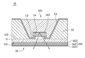
- the LED package structure 10 is a flip-chip LED package structure, and comprises a substrate 11 , a housing 12 , two electrodes 13 , and an LED chip 14 .
- the substrate 11 is a transparent flat layer, for allowing light emitted by the LED chip 14 passing therethrough.
- the substrate 11 has a supporting face 112 and a light-emergent face 114 opposite to the supporting face 112 .
- the housing 12 and the two electrodes 13 are disposed on the supporting face 112 .
- a phosphor layer 16 is further provided to spread on the light-emergent face 114 .
- the substrate 11 is made of material with high light permeability, such as silicon dioxide, silicon nitride, diamond, diamond-like material, sapphire, polymer material or quartz.
- the housing 12 is formed on the supporting face 112 of the substrate 11 .
- a downwardly tapered receiving portion 12 a is defined at a center of the housing 12 .
- the receiving portion 12 a extends through the housing 12 , whereby a part of the supporting face 112 is exposed via the receiving portion 12 a .
- the housing 12 has a good capability of heat dissipation, and is made of material selected from aluminum nitride, silicon, boron nitride or graphite.
- the receiving portion 12 a has a periphery surrounding the LED chip 14 .
- the two electrodes 13 are attached on the housing 12 .
- the two electrodes 13 are spaced from and disposed opposite to each other.
- Each of the two electrodes 13 extends from a top face of the housing 12 , along the periphery of the receiving portion 12 a and to the supporting face 112 of the substrate 11 .
- the electrodes 13 are made of material selected from aluminum, gold, copper, nickel or indium tin dioxide.
- the LED chip 14 is received in the receiving portion 12 a , and disposed on the supporting face 112 of the substrate 11 .
- the LED chip 14 is electrically connected to the two electrodes 13 .
- a reflecting layer 140 is further provided to cover a top portion of the LED chip 14 , whereby light emitted by the LED chip 14 can be reflected downwardly toward the transparent substrate 11 .
- the reflecting layer 140 is formed on the LED chip 14 by attachment, electroplating deposition, sputtering deposition or evaporation deposition.
- the reflecting layer 140 is made of material selected from gold, titanium, chrome, silver, aluminum, or an alloy thereof.
- the phosphor layer 16 which has a structure of a film is formed on the light-emergent face 114 of the substrate 11 by attachment or coating.
- the phosphor layer 16 is a multilayer structure, and comprises a plurality of layers 160 each having a specific light wavelength conversion range to emit a light with a predetermined color. The values of the wavelength of the lights emitted by the layers 160 gradually decrease along a direction away from the substrate 11 .
- the phosphor layer 16 comprises a first layer 161 formed on the light-emergent face 114 , a second layer 162 formed on the first layer 161 , and a third layer 163 formed on the second layer 162 .
- the first layer 161 has first phosphorous compound therein whereby the first layer 161 emits red light
- the second layer 162 has second phosphorous compound therein whereby the second layer 162 emits green light
- the third layer 163 has third phosphorous compound therein whereby the third layer 163 emits blue light.
- an LED package structure 20 in accordance with a second embodiment of this disclosure is shown.
- the LED package structure 20 is mostly similar to the LED package structure 10 , and comprises a substrate 21 , a housing 22 , two electrodes 23 , and an LED chip 24 .
- a height of the housing 22 is equal to that of the LED chip 24 , whereby the LED package structure 20 is more compact and has a low profile.
Abstract
An LED package structure includes a transparent substrate having a supporting face and a light-emergent face opposite to the supporting face, a housing disposed on the supporting face, two electrodes disposed on the housing, an LED chip disposed on the supporting face and electrically connected to the two electrodes, a reflecting layer covering the LED chip to reflect light emitted by the LED chip toward the transparent substrate, and a phosphor layer formed on the light-emergent face of the substrate. The phosphor layer includes a plurality of layers each having a specific light wavelength conversion range to generate a light with a predetermined color.
Description
1. Technical Field
The present disclosure relates to an optical component, and particularly, to a light emitting diode (LED) package structure.
2. Description of Related Art
Presently, LEDs are preferred for use in non-emissive display devices than CCFLs (cold cathode fluorescent lamp) due to their high brightness, long lifespan, and wide color range. A typical LED package structure includes a substrate, an LED chip disposed on the substrate and an encapsulation material encapsulating the LED chip. The encapsulation material includes a resin and various phosphorous compounds doped within the resin, which can turn portions of light emitted from the LED chip into desired color. However, as various phosphorous compounds are mixed together, they would generate light with different wavelengths interfering each other, thereby decreasing the light-emitting efficiency of the LED package structure.
Accordingly, it is desirable to provide an LED package structure which can overcome the described limitations.
Many aspects of the disclosure can be better understood with reference to the drawings. The components in the drawings are not necessarily drawn to scale, the emphasis instead being placed upon clearly illustrating the principles of the present disclosure. Moreover, in the drawings, like reference numerals designate corresponding parts throughout the views.
Referring to FIG. 1 , a light emitting diode (LED) package structure 10 in accordance with a first embodiment of the disclosure is illustrated. The LED package structure 10 is a flip-chip LED package structure, and comprises a substrate 11, a housing 12, two electrodes 13, and an LED chip 14.
The substrate 11 is a transparent flat layer, for allowing light emitted by the LED chip 14 passing therethrough. The substrate 11 has a supporting face 112 and a light-emergent face 114 opposite to the supporting face 112. The housing 12 and the two electrodes 13 are disposed on the supporting face 112. A phosphor layer 16 is further provided to spread on the light-emergent face 114. The substrate 11 is made of material with high light permeability, such as silicon dioxide, silicon nitride, diamond, diamond-like material, sapphire, polymer material or quartz.
The housing 12 is formed on the supporting face 112 of the substrate 11. A downwardly tapered receiving portion 12 a is defined at a center of the housing 12. The receiving portion 12 a extends through the housing 12, whereby a part of the supporting face 112 is exposed via the receiving portion 12 a. The housing 12 has a good capability of heat dissipation, and is made of material selected from aluminum nitride, silicon, boron nitride or graphite. The receiving portion 12 a has a periphery surrounding the LED chip 14. The two electrodes 13 are attached on the housing 12. The two electrodes 13 are spaced from and disposed opposite to each other. Each of the two electrodes 13 extends from a top face of the housing 12, along the periphery of the receiving portion 12 a and to the supporting face 112 of the substrate 11. The electrodes 13 are made of material selected from aluminum, gold, copper, nickel or indium tin dioxide.
The LED chip 14 is received in the receiving portion 12 a, and disposed on the supporting face 112 of the substrate 11. The LED chip 14 is electrically connected to the two electrodes 13. A reflecting layer 140 is further provided to cover a top portion of the LED chip 14, whereby light emitted by the LED chip 14 can be reflected downwardly toward the transparent substrate 11. The reflecting layer 140 is formed on the LED chip 14 by attachment, electroplating deposition, sputtering deposition or evaporation deposition. The reflecting layer 140 is made of material selected from gold, titanium, chrome, silver, aluminum, or an alloy thereof.
The phosphor layer 16, which has a structure of a film is formed on the light-emergent face 114 of the substrate 11 by attachment or coating. The phosphor layer 16 is a multilayer structure, and comprises a plurality of layers 160 each having a specific light wavelength conversion range to emit a light with a predetermined color. The values of the wavelength of the lights emitted by the layers 160 gradually decrease along a direction away from the substrate 11. In the embodiment of this disclosure, the phosphor layer 16 comprises a first layer 161 formed on the light-emergent face 114, a second layer 162 formed on the first layer 161, and a third layer 163 formed on the second layer 162. The first layer 161 has first phosphorous compound therein whereby the first layer 161 emits red light, the second layer 162 has second phosphorous compound therein whereby the second layer 162 emits green light, and the third layer 163 has third phosphorous compound therein whereby the third layer 163 emits blue light.
Referring to FIG. 2 , an LED package structure 20 in accordance with a second embodiment of this disclosure is shown. The LED package structure 20 is mostly similar to the LED package structure 10, and comprises a substrate 21, a housing 22, two electrodes 23, and an LED chip 24. In the second embodiment of this disclosure, a height of the housing 22 is equal to that of the LED chip 24, whereby the LED package structure 20 is more compact and has a low profile.
It is to be understood, however, that even though numerous characteristics and advantages of the present embodiments have been set fourth in the foregoing description, together with details of the structures and functions of the embodiments, the disclosure is illustrative only, and changes may be made in details, especially in matters of shape, size, and arrangement of parts within the principles of the disclosure to the full extent indicated by the broad general meaning of the terms in which the appended claims are expressed.
Claims (14)
1. A light emitting diode (LED) package structure, comprising:
a transparent substrate having a supporting face and a light-emergent face opposite to the supporting face;
a housing disposed on the supporting face;
two electrodes disposed on the housing;
an LED chip disposed on the supporting face and electrically connected to the two electrodes;
a reflecting layer covering the LED chip to reflect light emitted by the LED chip toward the transparent substrate; and
a phosphor layer formed on the light-emergent face of the substrate, wherein the phosphor layer comprises a plurality of layers each having a specific light wavelength conversion range to emit a light with a predetermined color.
2. The LED package structure as described in claim 1 , wherein the substrate is made of material selected from one of silicon dioxide, silicon nitride, diamond, diamond-like material, sapphire, polymer material and quartz.
3. The LED package structure as described in claim 1 , wherein the substrate is a flat layer.
4. The LED package structure as described in claim 1 , wherein a receiving portion is defined at a center of the housing for receiving the LED chip therein.
5. The LED package structure as described in claim 4 , wherein the receiving portion extends through the housing, whereby a part of the supporting face is exposed via the receiving portion.
6. The LED package structure as described in claim 1 , wherein the receiving portion has a periphery surrounding the LED chip.
7. The LED package structure as described in claim 6 , wherein each of the two electrodes extends from a top face of the housing along the periphery of the receiving portion to the supporting face of the substrate.
8. The LED package structure as described in claim 1 , wherein the housing is made of material selected from one of aluminum nitride, silicon, boron nitride and graphite.
9. The LED package structure as described in claim 1 , wherein the electrodes are made from materials selected from aluminum, gold, copper, nickel, and indium tin dioxide.
10. The LED package structure as described in claim 1 , wherein the phosphor layer has a structure of a film and is formed on the light-emergent face of the substrate by one of attachment and coating.
11. The LED package structure as described in claim 1 , wherein values of the wavelength of the lights emitted by the layers gradually decrease along a direction away from the substrate.
12. The LED package structure as described in claim 11 , wherein the phosphor layer comprises a first layer formed on the light-emergent face, a second layer formed on the first layer, and a third layer formed on the second layer.
13. The LED package structure as described in claim 12 , wherein the first layer comprises a first phosphorous compound whereby the first layer emits red light, the second layer comprises a second phosphorous compound whereby the second layer emits green light, and the third layer comprises a third phosphorous compound whereby the third layer emits blue light.
14. The LED package structure as described in claim 1 , wherein a height of the housing is equal to that of the LED chip.
Applications Claiming Priority (3)
| Application Number | Priority Date | Filing Date | Title |
|---|---|---|---|
| CN201010227947 | 2010-07-15 | ||
| CN201010227947.8A CN102339935B (en) | 2010-07-15 | 2010-07-15 | Flip-chip-type LED (light-emitting diode) package structure |
| CN201010227947.8 | 2010-07-15 |
Publications (2)
| Publication Number | Publication Date |
|---|---|
| US20120012872A1 US20120012872A1 (en) | 2012-01-19 |
| US8222662B2 true US8222662B2 (en) | 2012-07-17 |
Family
ID=45466245
Family Applications (1)
| Application Number | Title | Priority Date | Filing Date |
|---|---|---|---|
| US12/975,232 Expired - Fee Related US8222662B2 (en) | 2010-07-15 | 2010-12-21 | LED package structure |
Country Status (2)
| Country | Link |
|---|---|
| US (1) | US8222662B2 (en) |
| CN (1) | CN102339935B (en) |
Cited By (3)
| Publication number | Priority date | Publication date | Assignee | Title |
|---|---|---|---|---|
| US20140124822A1 (en) * | 2012-11-05 | 2014-05-08 | Ledengin, Inc. | Graphite-containing substrates for led packages |
| US9472740B2 (en) | 2014-07-28 | 2016-10-18 | Samsung Electronics Co., Ltd. | Light emitting diode package and lighting device using the same |
| US20180257930A1 (en) * | 2014-07-17 | 2018-09-13 | Texas Instruments Incorporated | Optical electronics device |
Families Citing this family (7)
| Publication number | Priority date | Publication date | Assignee | Title |
|---|---|---|---|---|
| TWI367582B (en) * | 2008-12-01 | 2012-07-01 | Epistar Corp | Multi-colors package with single chip |
| TW201336114A (en) * | 2012-02-22 | 2013-09-01 | 矽品精密工業股份有限公司 | Semiconductor package and method of forming same |
| CN102945909B (en) * | 2012-11-08 | 2015-05-20 | 杭州天柱科技有限公司 | Total space white light LED (light emitting diode) device |
| KR101691818B1 (en) * | 2014-06-19 | 2017-01-03 | 삼성디스플레이 주식회사 | Light source module and backlight unit comprising the same |
| DE102018103748A1 (en) * | 2018-02-20 | 2019-08-22 | Osram Opto Semiconductors Gmbh | RADIATION-EMITTING COMPONENT AND METHOD FOR PRODUCING A RADIATION-EMITTING COMPONENT |
| CN110335931B (en) * | 2019-07-05 | 2020-12-01 | 开发晶照明(厦门)有限公司 | Photoelectric device and manufacturing method thereof |
| KR102511747B1 (en) * | 2021-07-16 | 2023-03-20 | 주식회사 글로벌테크놀로지 | Led package, semiconductor chip mounted on the led package and method for fabricating the same |
Citations (9)
| Publication number | Priority date | Publication date | Assignee | Title |
|---|---|---|---|---|
| US5813753A (en) * | 1997-05-27 | 1998-09-29 | Philips Electronics North America Corporation | UV/blue led-phosphor device with efficient conversion of UV/blues light to visible light |
| US6703780B2 (en) * | 2001-01-16 | 2004-03-09 | General Electric Company | Organic electroluminescent device with a ceramic output coupler and method of making the same |
| US6964877B2 (en) * | 2003-03-28 | 2005-11-15 | Gelcore, Llc | LED power package |
| US7183577B2 (en) * | 1999-09-27 | 2007-02-27 | Philips Lumileds Lighting Company, Llc | Thin film phosphor-converted light emitting diode device |
| US7382091B2 (en) * | 2005-07-27 | 2008-06-03 | Lung-Chien Chen | White light emitting diode using phosphor excitation |
| US20080211993A1 (en) * | 2007-03-01 | 2008-09-04 | Oki Data Corporation | Led backlight device and lcd device |
| US20090152582A1 (en) * | 2007-12-12 | 2009-06-18 | Foxsemicon Integrated Technology, Inc. | Light emitting diode |
| US20110012157A1 (en) * | 2009-02-26 | 2011-01-20 | Bridgelux, Inc. | Transparent heat spreader for leds |
| US8080828B2 (en) * | 2006-06-09 | 2011-12-20 | Philips Lumileds Lighting Company, Llc | Low profile side emitting LED with window layer and phosphor layer |
Family Cites Families (6)
| Publication number | Priority date | Publication date | Assignee | Title |
|---|---|---|---|---|
| JPH0725060A (en) * | 1993-06-25 | 1995-01-27 | Matsushita Electric Ind Co Ltd | Optical printing head and manufacture thereof |
| US6835960B2 (en) * | 2003-03-03 | 2004-12-28 | Opto Tech Corporation | Light emitting diode package structure |
| CN100481532C (en) * | 2004-01-21 | 2009-04-22 | 晶元光电股份有限公司 | Light emitting diode element, crystal coated light emitting diode packaging structure and light reflection structure |
| CN101562227B (en) * | 2005-05-30 | 2010-12-08 | 夏普株式会社 | Light emitting device and method of manufacturing the same |
| KR20090104860A (en) * | 2007-02-15 | 2009-10-06 | 파나소닉 전공 주식회사 | Led package and structure for mounting three-dimensional circuit component |
| CN101719491B (en) * | 2009-10-27 | 2011-06-15 | 东莞市精航科技有限公司 | Structure and method for encapsulating light-emitting diode |
-
2010
- 2010-07-15 CN CN201010227947.8A patent/CN102339935B/en not_active Expired - Fee Related
- 2010-12-21 US US12/975,232 patent/US8222662B2/en not_active Expired - Fee Related
Patent Citations (10)
| Publication number | Priority date | Publication date | Assignee | Title |
|---|---|---|---|---|
| US5813753A (en) * | 1997-05-27 | 1998-09-29 | Philips Electronics North America Corporation | UV/blue led-phosphor device with efficient conversion of UV/blues light to visible light |
| US7183577B2 (en) * | 1999-09-27 | 2007-02-27 | Philips Lumileds Lighting Company, Llc | Thin film phosphor-converted light emitting diode device |
| US6703780B2 (en) * | 2001-01-16 | 2004-03-09 | General Electric Company | Organic electroluminescent device with a ceramic output coupler and method of making the same |
| US6964877B2 (en) * | 2003-03-28 | 2005-11-15 | Gelcore, Llc | LED power package |
| US7382091B2 (en) * | 2005-07-27 | 2008-06-03 | Lung-Chien Chen | White light emitting diode using phosphor excitation |
| US8080828B2 (en) * | 2006-06-09 | 2011-12-20 | Philips Lumileds Lighting Company, Llc | Low profile side emitting LED with window layer and phosphor layer |
| US20080211993A1 (en) * | 2007-03-01 | 2008-09-04 | Oki Data Corporation | Led backlight device and lcd device |
| US20090152582A1 (en) * | 2007-12-12 | 2009-06-18 | Foxsemicon Integrated Technology, Inc. | Light emitting diode |
| US7728344B2 (en) * | 2007-12-12 | 2010-06-01 | Foxsemicon Integrated Technology, Inc. | Light emitting diode |
| US20110012157A1 (en) * | 2009-02-26 | 2011-01-20 | Bridgelux, Inc. | Transparent heat spreader for leds |
Cited By (6)
| Publication number | Priority date | Publication date | Assignee | Title |
|---|---|---|---|---|
| US20140124822A1 (en) * | 2012-11-05 | 2014-05-08 | Ledengin, Inc. | Graphite-containing substrates for led packages |
| US9634214B2 (en) * | 2012-11-05 | 2017-04-25 | Ledengin, Inc. | Graphite-containing substrates for LED packages |
| US20180257930A1 (en) * | 2014-07-17 | 2018-09-13 | Texas Instruments Incorporated | Optical electronics device |
| US10894712B2 (en) * | 2014-07-17 | 2021-01-19 | Texas Instruments Incorporated | Optical electronics device |
| US11667523B2 (en) | 2014-07-17 | 2023-06-06 | Texas Instruments Incorporated | Optical electronics device |
| US9472740B2 (en) | 2014-07-28 | 2016-10-18 | Samsung Electronics Co., Ltd. | Light emitting diode package and lighting device using the same |
Also Published As
| Publication number | Publication date |
|---|---|
| CN102339935A (en) | 2012-02-01 |
| US20120012872A1 (en) | 2012-01-19 |
| CN102339935B (en) | 2015-07-08 |
Similar Documents
| Publication | Publication Date | Title |
|---|---|---|
| US8222662B2 (en) | LED package structure | |
| TWI433344B (en) | Light emitting apparatus and illuminating apparatus | |
| KR100620844B1 (en) | Light-emitting apparatus and illuminating apparatus | |
| JP5196711B2 (en) | LIGHT EMITTING DEVICE AND LIGHTING DEVICE USING THE SAME | |
| US7888698B2 (en) | Photoelectric semiconductor device capable of generating uniform compound lights | |
| US9048404B2 (en) | Thin flat solid state light source module | |
| JP4698412B2 (en) | Light emitting device and lighting device | |
| JP3898721B2 (en) | Light emitting device and lighting device | |
| JP2006237264A (en) | Light emitting device and lighting apparatus | |
| JP2008251663A (en) | Light-emitting device and illumination apparatus | |
| US20150349216A1 (en) | Light emitting diode package structure | |
| US8445920B1 (en) | Light emitting diode | |
| KR20160098580A (en) | Optical device and light source module having the same | |
| JP2005159262A (en) | Package for housing light emitting element, light emitting device, and lighting system | |
| US20060243995A1 (en) | White light emitting diode device | |
| JP2006093399A (en) | Light-emitting device, its manufacturing method and luminaire | |
| JP2005277331A (en) | Light emitting device and lighting device | |
| KR100610278B1 (en) | High Brightness White LED And Preparation Method For The Same | |
| US20160254423A1 (en) | Non-magnified led for high center-beam candle power | |
| KR101666844B1 (en) | Optical device and light source module having the same | |
| JP4868960B2 (en) | Light emitting device and manufacturing method thereof | |
| JP2005310911A (en) | Package for housing light emitting element, light emitting device, and lighting apparatus | |
| US8878208B2 (en) | Illuminating device | |
| US20180102459A1 (en) | Light emitting diode chip scale packaging structure and direct type backlight module | |
| US20120175656A1 (en) | Light emitting diode package |
Legal Events
| Date | Code | Title | Description |
|---|---|---|---|
| AS | Assignment |
Owner name: ADVANCED OPTOELECTRONIC TECHNOLOGY, INC., TAIWAN Free format text: ASSIGNMENT OF ASSIGNORS INTEREST;ASSIGNORS:SHEN, CHIA-HUI;HUNG, TZU-CHIEN;TSANG, JIAN-SHIHN;REEL/FRAME:025539/0130 Effective date: 20101216 |
|
| REMI | Maintenance fee reminder mailed | ||
| LAPS | Lapse for failure to pay maintenance fees | ||
| STCH | Information on status: patent discontinuation |
Free format text: PATENT EXPIRED DUE TO NONPAYMENT OF MAINTENANCE FEES UNDER 37 CFR 1.362 |
|
| FP | Lapsed due to failure to pay maintenance fee |
Effective date: 20160717 |