US8225252B2 - Systems, methods, apparatus and computer readable mediums for use in association with systems having interference - Google Patents

Systems, methods, apparatus and computer readable mediums for use in association with systems having interference Download PDF

Info

Publication number
US8225252B2
US8225252B2 US12/823,723 US82372310A US8225252B2 US 8225252 B2 US8225252 B2 US 8225252B2 US 82372310 A US82372310 A US 82372310A US 8225252 B2 US8225252 B2 US 8225252B2
Authority
US
United States
Prior art keywords
location
interference
signals
communication interface
estimate
Prior art date
Legal status (The legal status is an assumption and is not a legal conclusion. Google has not performed a legal analysis and makes no representation as to the accuracy of the status listed.)
Expired - Fee Related, expires
Application number
US12/823,723
Other versions
US20110316561A1 (en
Inventor
Alberto Alcocer Ochoa
Keith Raynard Tinsley
Current Assignee (The listed assignees may be inaccurate. Google has not performed a legal analysis and makes no representation or warranty as to the accuracy of the list.)
Intel Corp
Original Assignee
Intel Corp
Priority date (The priority date is an assumption and is not a legal conclusion. Google has not performed a legal analysis and makes no representation as to the accuracy of the date listed.)
Filing date
Publication date
Application filed by Intel Corp filed Critical Intel Corp
Assigned to INTEL CORPORATION reassignment INTEL CORPORATION ASSIGNMENT OF ASSIGNORS INTEREST (SEE DOCUMENT FOR DETAILS). Assignors: ALCOCER OCHOA, ALBERTO, TINSLEY, KEITH RAYNARD
Priority to US12/823,723 priority Critical patent/US8225252B2/en
Priority to JP2013515586A priority patent/JP5507758B2/en
Priority to EP11798933.5A priority patent/EP2585928B1/en
Priority to PCT/US2011/041657 priority patent/WO2011163495A2/en
Priority to CN201180027401.0A priority patent/CN102918514B/en
Priority to KR1020127033455A priority patent/KR101451613B1/en
Publication of US20110316561A1 publication Critical patent/US20110316561A1/en
Publication of US8225252B2 publication Critical patent/US8225252B2/en
Application granted granted Critical
Expired - Fee Related legal-status Critical Current
Adjusted expiration legal-status Critical

Links

Images

Classifications

    • GPHYSICS
    • G06COMPUTING; CALCULATING OR COUNTING
    • G06FELECTRIC DIGITAL DATA PROCESSING
    • G06F13/00Interconnection of, or transfer of information or other signals between, memories, input/output devices or central processing units
    • G06F13/14Handling requests for interconnection or transfer
    • GPHYSICS
    • G06COMPUTING; CALCULATING OR COUNTING
    • G06FELECTRIC DIGITAL DATA PROCESSING
    • G06F13/00Interconnection of, or transfer of information or other signals between, memories, input/output devices or central processing units
    • G06F13/38Information transfer, e.g. on bus
    • HELECTRICITY
    • H04ELECTRIC COMMUNICATION TECHNIQUE
    • H04BTRANSMISSION
    • H04B15/00Suppression or limitation of noise or interference

Definitions

  • Many systems include communication interfaces to allow devices within the system to communicate with one another and/or with other systems.
  • many computer systems include a communication interface that is sometimes referred to as a memory bus in order to transfer information (e.g., addresses and/or data) to and/or from a memory device within the system.
  • many computer systems also include a communication interface that is sometimes referred to as a peripheral component interconnect (PCI) bus, to transfer information to and/or from a peripheral and/or add-on device within a system.
  • PCI peripheral component interconnect
  • EMI electromagnetic interference
  • RFID radio frequency interference
  • FIG. 1 is a schematic, cutaway, side view of a system according to some embodiments.
  • FIG. 2 is a schematic plan view of a portion of a substrate according to some embodiments.
  • FIG. 3 is a schematic diagram of a portion of a system according to some embodiments.
  • FIG. 4 is a flow diagram of a method according to some embodiments.
  • FIG. 5 is a graphical representation of characteristics of Golay codes, in accordance with some embodiments.
  • FIG. 6 is a graphical representation of a portion of a method, in accordance with some embodiments.
  • FIG. 7 is a table representing interference detected at a location of interest, in accordance with some embodiments.
  • FIG. 8A is a graphical representation of characteristics of Gold codes, in accordance with some embodiments.
  • FIG. 8B is a schematic diagram of a maximum length shift register, in accordance with some embodiments.
  • FIG. 9 is a graphical representation of a portion of a method, in accordance with some embodiments.
  • FIG. 10 is a block diagram of an apparatus, in accordance with some embodiments.
  • FIG. 11 is a block diagram of an architecture, in accordance with some embodiments.
  • FIG. 1 is a schematic, cutaway, side view of one type of system 100 for which it may it may be desirable to identify a communication interface that results in a greatest amount (or at least one of the greatest amounts), an unacceptable amount and/or merely an undesirable amount of interference at a given location of interest, according to some embodiments.
  • the system 100 includes a first integrated circuit package 102 A, a second integrated circuit package 102 B and a circuit board 104 .
  • the first integrated circuit package 102 A includes an integrated circuit package substrate 106 A, a first integrated circuit die 108 A 1 , a second integrated circuit die 108 A 2 and a third integrated circuit die 108 A 3 .
  • the second integrated circuit package 102 B includes an integrated circuit package substrate 106 B and an integrated circuit die 108 B.
  • the first integrated circuit package 102 A and the second integrated circuit package 102 B may each include one or more other devices (not shown).
  • the integrated circuit package substrate 106 A may include a first outer surface 120 A and a second outer surface 122 A.
  • the first outer surface 120 A may define mounting areas 128 A 1 - 128 A 3 on which the integrated circuits die 108 A 1 - 108 A 2 are mounted include a plurality of contacts electrically connected to the electrical devices (sometimes referred to herein as components) mounted thereon.
  • mounting area 128 A 1 include contacts 138 electrically connected to the integrated circuit die 108 A 1 .
  • Mounting area 128 A 2 include contacts 138 electrically connected to the integrated circuit die 108 A 2 .
  • Mounting area 128 A 3 include contacts 138 electrically connected to the integrated circuit die 108 A 3 .
  • the second outer surface 122 A may overlay a fractional portion of the circuit board 104 and may define a mounting area 144 A mounted to the circuit board 104 .
  • the mounting area 144 A may include a plurality of contacts 154 electrically connected to the circuit board 104 .
  • the contacts 154 are soldered directly to the contacts 158 in order to mount and electrically connect the integrated circuit package 102 A thereto.
  • a socket may be disposed between the contacts 154 and contacts 158 .
  • the integrated circuit package substrate 106 B may include a first outer surface 120 B and a second outer surface 122 B.
  • the first outer surface 120 B may define a mounting area 128 B on which the integrated circuit die 108 B is mounted.
  • the mounting area 128 B may include a plurality of contacts electrically connected to the electrical devices (sometimes referred to herein as components) mounted thereon.
  • mounting area 128 B include contacts 138 electrically connected to the integrated circuit die 108 B.
  • the second outer surface 122 B may overlay a fractional portion of the circuit board 104 and may define a mounting area 144 B mounted to the circuit board 104 .
  • the mounting area 144 B may include a plurality of contacts 154 electrically connected to the circuit board 104 .
  • the contacts 154 are soldered directly to the contacts 158 in order to mount and electrically connect the integrated circuit package 102 B thereto.
  • a socket may be disposed between the contacts 154 and contacts 158 .
  • testing may be performed before the first integrated circuit package 102 A and/or the second integrated circuit package 102 B are mounted to the circuit board 104 so as to help avoid waste of resources in the event that either of the integrated circuit packages 102 A- 102 B is defective.
  • Some of the contacts 154 may conduct signals to and/or from the circuit board 104 . Others of the plurality of contacts 154 may conduct a supply voltage and/or ground to and/or from the integrated circuit packages 102 A- 102 B
  • the contacts 154 are arranged in an array sometimes referred to as a land grid array (LGA).
  • the contacts 154 and the contacts 158 are arranged in corresponding arrays such that each of the contacts 154 is in register with a respective one of the contacts 158 .
  • each of the arrays is a two dimensional array that includes a plurality of rows and a plurality of columns.
  • ball contacts 156 are joined to the second outer surface 122 A of the substrate 106 A and the second outer surface 122 B of the substrate 106 B and soldered to contacts 158 of the circuit board 104 in order to mount and electrically connect the integrated circuit packages 102 A- 102 B thereto.
  • the ball contacts 156 are arranged in an array sometimes referred to as a ball grid array (BGA).
  • the contacts 154 , the ball contacts 156 and the contacts 158 are arranged in corresponding arrays such that such that each of the contacts 154 is in register with a respective one of the contacts 156 and a respective one of the contacts 158 .
  • each of the arrays is a two dimensional array that includes a plurality of rows and a plurality of columns.
  • the substrate 106 A may further include a plurality of electrical conductors 162 , 164 , 166 , 167 (e.g., traces and/or vias).
  • the plurality of electrical conductors 162 , 164 , 166 may connect one or more of the contacts 138 to one or more of the contacts 154 (thereby electrically connecting one or more of the integrated circuit die 108 A 1 - 108 A 3 to the circuit board 104 ).
  • the plurality of electrical conductors 167 may electrically connect one or more of the contacts 138 electrically connected to the integrated circuit die 108 A 2 to one or more of the contacts 138 electrically connected to the integrated circuit die 108 A 3 (to electrically connect the integrated circuit die 108 A 2 to the integrated circuit die 108 A 3 ).
  • the electrical conductors 162 electrically connect one of the contacts 138 electrically connected to the integrated circuit die 108 A 1 to one of the contacts 154 electrically connected to the circuit board 104 .
  • the electrical conductors 164 electrically connect a group of the contacts 138 electrically connected to the integrated circuit die 108 A 1 to another one of the contacts 154 electrically connected to the circuit board 104 .
  • the electrical conductors 166 electrically connect a group of the contacts 138 electrically connected to the integrated circuit die 108 A 2 to another one of the contacts 154 electrically connected to the circuit board 104 .
  • the electrical conductors 162 conduct signals to and/or from the circuit board 104 .
  • the electrical conductors 164 conduct a supply voltage being supplied to the integrated circuit die 108 A 1 .
  • the electrical conductors 166 conduct a ground being supplied to the integrated circuit die 108 A 2 .
  • the electrical conductors 167 electrically connect one of the contacts 138 electrically connected to the integrated circuit die 108 A 2 to one of the contacts 138 electrically connected to the integrated circuit die 108 A 3 .
  • the plurality of electrical conductors 160 may also include one or more electrical conductors to electrically connect integrated circuit die 108 A 1 to integrated circuit die 108 A 2 , to electrically connect integrated circuit die 108 A 1 to integrated circuit die 108 A 3 , and/or to electrically connect any of the components to one or more other components.
  • Each of the integrated circuit die 108 A 1 - 108 A 3 , 108 B may include one or more integrated circuits disposed on a substrate.
  • integrated circuit die 108 A 1 includes one or more integrated circuits 168 A 1 disposed on substrate 169 A 1 .
  • Integrated circuit die 108 A 2 includes one or more integrated circuits 168 A 2 disposed on substrate 169 A 2 .
  • Integrated circuit die 108 A 3 includes one or more integrated circuits 168 A 3 disposed on substrate 169 A 3 .
  • Integrated circuit die 108 B includes one or more integrated circuits 168 B disposed on substrate 169 B.
  • the one or more integrated circuits may comprise active and/or passive components.
  • the substrate may comprise a semiconductor substrate and/or any other type of substrate.
  • the integrated circuit die 108 A 1 includes a first outer surface 170 A 1 and a second outer surface 172 A 1 .
  • the first outer surface 170 A 1 and the second outer surface 172 A 1 are opposite major outer surfaces, for example, as shown.
  • the first outer surface 170 A 1 may define a plurality of contacts 178 electrically connected to one or more of the one or more integrated circuits 168 of the integrated circuit die 108 A 1 .
  • the integrated circuit die 108 A 1 - 108 A 3 , 108 B may be mounted to the first outer surface 120 A, 120 B, respectively, of the substrate 106 A, 106 B, respectively.
  • bump contacts 179 are joined to the contacts 178 of the integrated circuit die 108 A 1 - 108 A 3 , 108 B and soldered to the contacts 138 of the substrate 106 A, 106 B, respectively, in order to mount and electrically connect the integrated circuit die 108 A 1 - 108 A 3 , 108 B, respectively, thereto.
  • testing is performed before the integrated circuit die-bump contact assembly is mounted to the substrates 106 A, 106 B so as to help avoid waste of resources in the event that one or more of the integrated circuit die 108 A 1 - 108 A 3 , 108 B is defective.
  • the contacts 138 , the contacts 178 and the bump contacts 179 are arranged in corresponding arrays such that such that each of the contacts 138 is in register with a respective one of the contacts 178 and a respective one of the bump contacts 179 .
  • each of the arrays is a two dimensional array that includes a plurality of rows and a plurality of columns. The number of rows in each array and/or the number of columns in each array may depend at least in part on a number of contacts 138 that may be desired for the integrated circuit die 108 A 1 - 108 A 3 , 108 B.
  • the first integrated circuit package 102 A and/or the second integrated circuit package 102 B may include wirebond type connections (sometimes referred to herein as bond wires) to one or more of the integrated circuit die in lieu of and/or in addition to the bump contacts 179 .
  • wirebond type connections sometimes referred to herein as bond wires
  • testing is performed before the integrated circuit die is mounted to the substrate 106 so as to help avoid waste of resources in the event that one or more of the integrated circuit die 108 A 1 - 108 A 3 , 108 B is defective.
  • the circuit board 104 includes a first outer surface 194 .
  • the first outer surface 194 comprises a first major outer surface.
  • the first outer surface 194 may define the plurality of contacts 158 electrically connected to the integrated circuit package 102 A and/or the second integrated circuit package 102 B.
  • the circuit board 104 may comprise any type of circuit board.
  • the circuit board 104 comprises a multi-layer laminate that is rigid and/or at least substantially rigid so as to provide support for the components mounted thereon.
  • the circuit board 104 comprises a printed circuit board.
  • the circuit board 104 comprises a processor board and/or a motherboard.
  • the circuit board 104 is attached to a chassis (not shown) or some other structure (not shown).
  • one or more components of the integrated circuit packages 102 A, 102 B are selected so as to keep the overall dimensions of the integrated circuit packages 102 A, 102 B within predetermined limits.
  • one or both of the integrated circuit package 102 A, 102 B has a height 195 (e.g., measured from the first outer surface 194 of the circuit board 104 ) of not greater than 2.85 millimeters (mm).
  • the system 100 further includes a heat sink 196 , which may improve thermal conductivity between the system 100 and a surrounding environment in which the system may be employed, and may thereby help make it possible for the system to deliver greater performance (e.g., speed) all else being equal.
  • the heat sink 196 comprises a one piece, integrally formed, “finned” heat sink.
  • the fins which may have any size and shape, may improve thermal conductivity between the heat sink 196 and the surrounding environment.
  • the heat sink 196 comprises metal so as to help provide a high thermal conductivity.
  • the heat sink 196 may be attached to one or more other structures (not shown).
  • the integrated circuit package may further include mechanical clips (not shown) that mechanically connect the heat sink 196 to the circuit board 104 .
  • a thermal interface material (not shown) may be disposed between the integrated circuit die 108 A 2 and the heat sink 196 .
  • the thermal interface material is used to mount the heat sink 196 to the integrated circuit die 108 A 2 and/or to another portion of the integrated circuit package 102 A.
  • the integrated circuit package 102 A and/or the integrated circuit package may include a lid 198 A, 198 B, respectively.
  • the lid 198 A and the substrate 106 A collectively define a hermetically seal.
  • the lid 198 B and the substrate 106 B collectively define a hermetically seal.
  • the substrates 106 A, 106 B, and the integrated circuit die 108 A 1 - 108 A 3 , 108 B are shown having a surface mountable form, in some embodiments, the substrates 106 A- 106 B and the integrated circuit die 108 A 1 - 108 A 3 , 108 B may not have a surface mountable form.
  • one or more of the integrated circuit die 108 A 1 - 108 A 3 , 108 B comprises a memory device for storing data and/or other information.
  • the memory device comprises a Single Data Rate Random Access Memory, a Double Data Rate Random Access Memory or a Programmable Read Only Memory.
  • one or more additional integrated circuit packages is mounted on the printed circuit board 104 .
  • one or more of the conductors shown in FIG. 1 belongs to a communication interface. In some embodiments, a plurality of communication interfaces may be employed.
  • FIG. 2 is a schematic plan view of a portion 200 of the substrate 106 A, according to some embodiments.
  • the mounting area 128 A 1 for the integrated circuit die 108 A 1 may have a length 202 of about 10.5 mm and a width 204 of about 10.5 mm.
  • a mounting area for 132 for capacitors may have a width 206 of about 2.7 mm.
  • a distance 208 between the mounting area 128 A 1 for the integrated circuit die 108 A 1 and the mounting areas 132 may be about 2 mm.
  • the first outer surface 120 A of the substrate 106 A may further define areas 212 , 214 .
  • the area 212 may have a width 215 of about 1.7 mm.
  • the area 214 may have a width 216 of about 2.7 mm.
  • a distance 218 between the mounting area 128 A 1 for the integrated circuit die 108 A 1 and the area 212 may be about 3 mm.
  • a distance 220 between the mounting area 128 for the integrated circuit die 108 A 1 and the area 214 may be about 2 mm.
  • the contacts 138 are represented by circles however the contacts 138 may have any configuration.
  • the integrated circuit packages 102 A- 102 B may be fabricated using any suitable fabrication technique and may provide any functions to system 100 .
  • one or more circuits of one or more of the integrated circuit die 108 A 1 - 108 A 3 , 108 B define a processor.
  • a processor comprises a microprocessor and/or communication processor.
  • a communication processor is adapted to perform one or more communication intensive processes.
  • one or more of the integrated circuit die comprises a processor.
  • the first integrated circuit die 108 A 1 and the second integrated circuit die 108 A 2 comprise a first processor and a second processor, respectively.
  • the first integrated circuit die 108 A 1 and the second integrated circuit die 108 A 2 comprise a processor and a co-processor, respectively.
  • the first integrated circuit die 108 A 1 and the second integrated circuit die 108 A 2 comprise a processor and a graphics processor, respectively.
  • one or more of the integrated circuit die, e.g., the third integrated circuit die 108 A 3 comprises a memory device.
  • the third integrated circuit die 108 A 3 comprises a DDR3 type of memory device.
  • one or more of the integrated circuit die, e.g., integrated circuit die 108 B, comprises a peripheral and/or add-on device.
  • the integrated circuit die 108 B comprises an application specific integrated circuit (ASIC).
  • ASIC application specific integrated circuit
  • a processor may comprise any type of processor.
  • a processor may be programmable or non programmable, general purpose or special purpose, dedicated or non dedicated, distributed or non distributed, shared or not shared, and/or any combination thereof.
  • a processor may include, but is not limited to, hardware, software, firmware, and/or any combination thereof.
  • Software may include, but is not limited to, instructions stored on a computer readable medium, such as, for example, punch cards, paper tape, magnetic or optical disk, magnetic or optical tape, CD-ROM, DVD, RAM, EPROM, or ROM.
  • a processor may employ continuous signals, periodically sampled signals, and/or any combination thereof.
  • a microprocessor may comprise any type of microprocessor.
  • a microprocessor may be programmable or non programmable, general purpose or special purpose, dedicated or non dedicated, distributed or non distributed, shared or not shared, and/or any combination thereof.
  • a microprocessor may include, but is not limited to, hardware, software, firmware, and/or any combination thereof.
  • Software may include, but is not limited to, instructions stored on a computer readable medium, such as, for example, punch cards, paper tape, magnetic or optical disk, magnetic or optical tape, CD-ROM, DVD, RAM, EPROM, or ROM.
  • a microprocessor may employ continuous signals, periodically sampled signals, and/or any combination thereof.
  • a communication processor may comprise any type of communication processor.
  • a communication processor may be programmable or non programmable, general purpose or special purpose, dedicated or non dedicated, distributed or non distributed, shared or not shared, and/or any combination thereof.
  • a communication processor may include, but is not limited to, hardware, software, firmware, and/or any combination thereof.
  • Software may include, but is not limited to, instructions stored on a computer readable medium, such as, for example, punch cards, paper tape, magnetic or optical disk, magnetic or optical tape, CD-ROM, DVD, RAM, EPROM, or ROM.
  • a communication processor may employ continuous signals, periodically sampled signals, and/or any combination thereof.
  • some of the electrical conductors within the system 100 are part of one or more communication interfaces that connect to one or more of the integrated circuit die 108 A 1 - 108 A 3 , 1088 .
  • FIG. 3 is a schematic diagram of a portion 300 of the system 100 showing a plurality of communication interfaces that may connect to the integrated circuit die 108 A 1 - 108 A 3 , 108 B, according to some embodiments.
  • the system 100 may include a first communication interface 302 , a second communication interface 304 and a third communication interface 306 .
  • the first communication interface 302 may have a first end connected to the first integrated circuit die 108 A 1 of the first integrated circuit package 102 A and a second end connected to the second integrated circuit die 108 A 2 of the first integrated circuit package 102 A to thereby connect the first integrated circuit die 108 A 1 of the first integrated circuit package 102 A to the second integrated circuit die 108 A 2 of the first integrated circuit package 102 A.
  • the second communication interface 304 may have a first end connected to the second integrated circuit die 108 A 2 of the first integrated circuit package 102 A and a second end connected to the third integrated circuit die 108 A 3 of the first integrated circuit package 102 A to thereby connect the second integrated circuit die 108 A 2 of the first integrated circuit package 102 A to the third integrated circuit die 108 A 3 of the first integrated circuit package 102 A.
  • the third communication interface 306 may have a first end connected to the first integrated circuit die 108 A 1 of the first integrated circuit package 102 A and a second end connected to the integrated circuit die 108 B of the second integrated circuit package 102 B to thereby connect the first integrated circuit die 108 A 1 of the first integrated circuit package 102 A to the integrated circuit die 108 B of the second integrated circuit package 102 B.
  • Each of the communication interfaces may include any number of electrical conductors. In some embodiments, each of the communication interfaces a plurality of conductors. However, in some other embodiments, one or more of the communication interfaces may include only one electrical conductor.
  • each of the communication interfaces 302 - 306 is internal to the system 100 and may therefore be referred to as internal communication interfaces for the system 100 .
  • the first communication interface 302 and the second communication interface 304 are also internal to the first integrated circuit package 102 A and may therefore also be referred to as internal communication interfaces for the first integrated circuit package 102 A.
  • the third communication interface extends outside the first integrated circuit package 102 A and may therefore also be referred to as an external communication interface for the first integrated circuit package 102 A.
  • one or more of the communication interfaces may connect more than two integrated circuit die. In some embodiments, one or more of the communication interfaces 302 - 306 may extend outside of the system. In some embodiments, one or more other communication interfaces may be employed with or without one or more of the communication interfaces 302 - 306 .
  • the communication interfaces may comprise any type of communication interfaces.
  • one or more of the plurality of communication interfaces is a bus and/or an interconnection (e.g., a wired interconnection).
  • one or more of the communication interfaces is not limited to a bus and/or wired interconnection.
  • one or more of the communication interfaces comprises a memory bus to transfer information (e.g., addresses and/or data) to and/or from one or more memory devices within the system.
  • one or more of the integrated circuit die e.g., the third integrated circuit die 108 A 3 , comprises a memory device.
  • the memory bus comprises a DDR3 type of memory bus.
  • one or more of the communication interfaces comprises a PCI bus to transfer information to and/or from one or more peripheral and/or add-on devices.
  • one or more of the integrated circuit die e.g., integrated circuit die 108 B, comprises a peripheral and/or add-on device.
  • the PCI bus comprises a PCI Express bus.
  • FIG. 4 is a flow diagram of a method 400 according to some embodiments.
  • the method 400 may be used in identifying a communication interface that results in a greatest amount (or at least one of the greatest amounts), an unacceptable amount and/or merely an undesirable amount of interference at a given location of interest, according to some embodiments.
  • one or more portions of method 400 may be performed by an integrated circuit manufacturer.
  • one or more portions of method 400 may be performed by a system integrator.
  • one or more portions of method 400 may be performed manually.
  • the method 400 is not limited to the order shown in the flow diagram. Rather, embodiments of the method 400 may be performed in any order that is practicable. For that matter, unless stated otherwise, any method disclosed herein may be performed in any order that is practicable.
  • the method may include characterizing a plurality of channels, each of the plurality of channels being a channel between a location and a respective one of the plurality of communication interfaces.
  • a location and/or location of interest may comprise any type of location and/or location of interest, respectively.
  • a location and/or location of interest may be as small as a single point in space.
  • a location and/or location of interest may comprise a region and/or region of interest, respectively, that is larger than a single point in space.
  • a location and/or location of interest may comprise a three dimensional region that is as large as test personnel feel is appropriate and/or may be desired to accomplish a particular objective.
  • characterizing a channel between a location and a respective one of the communication interfaces comprises: dividing conductors of the respective one of the communication interface into groups; supplying signals to one of the groups at a time, and for each of the groups, detecting interference that occurs at the location as a result of emissions radiated from the group while the signals are supplied thereto and thereafter characterizing a channel between the location and the group.
  • a channel between the location and a group of conductors is characterized by estimating a channel power delay profile (PDP) or other statistical measure of average power or statistical measure of behavior based at least in part on the interference that was detected at the location of interest with the signals supplied to the group.
  • PDP channel power delay profile
  • each of the groups has a same number of conductors. In some embodiments, the number of conductors in each group is two (sometimes referred to as a pair of conductors).
  • the signals are Golay encoded signals. If the number of conductors in a group is equal to two, a first Golay encoded signal may be supplied to a first conductor in the group and a second Golay encoded signals may be supplied to a second conductor in the group.
  • the Golay encoded signals may have the characteristics shown in FIG. 5 , which is a representation of channel sounding characteristics of Golay Complementary Codes, in accordance with some embodiments.
  • R X stands for the autocorrelation of the code X
  • N is the length of the sequence
  • ⁇ (n) is the delta function
  • n denotes the time index.
  • there is not so easy way to create this pair of sequences but a set of 8-bit long codes appears in Table 1, which is a list of 8-bit long Golay complementary codes, and it can be used to create larger GCC.
  • Sequence B 1 00011101 00010010 2 01001000 00011101 3 00010010 10111000 4 11101101 00011101 5 11101101 11100010 6 01000111 01001000 7 10111000 00010010 8 10111000 01001000
  • larger codes can be created as follows: as 1 st sequence consider [A B] and then [A-B] for the second.
  • FIG. 6 is a graphical representation 600 showing the above with Golay encoded signals, in accordance with some embodiments.
  • a communication interface 602 i.e., a DDR3 BUS or other communication interface, includes a plurality of conductors, e.g., conductors 602 , 604 , 606 , 608 .
  • the plurality of conductors may be divided into groups, e.g., 610 , 612 .
  • a first signal i.e., GOLAY A or other signal
  • a second signal i.e., GOLAY B or other signal, may be supplied to the second conductor 604 in the group.
  • a transmitter 613 may be used to supply the signals.
  • the transmitter 613 is electrically connected to the group of conductors.
  • the transmitter 613 comprises a plurality of transmitters, e.g., 613 A, 613 B.
  • the transmitter 613 is disposed within the system 100 .
  • the transmitter 613 is disposed within an integrated circuit package, e.g., the first integrated circuit package 102 A or the second integrated circuit package 102 B.
  • the transmitter 613 may comprise circuitry within the system 100 and/or within the first integrated circuit package 102 A or the second integrated circuit package 102 B.
  • the signals supplied to the group may result in interference 614 , which may have different characteristics at different locations.
  • the interference may be detected at one or more locations of interest, e.g., location 616 .
  • a graph 620 has a waveform 622 representing the interference that may be detected at location 616 , in accordance with some embodiments.
  • a receiver 623 may be used to detect the interference at location 616 .
  • the receiver may comprise a near field scanner antenna (NFS).
  • the receiver 623 comprises a plurality of receivers, e.g., 623 A, 623 B.
  • the receiver 623 may or may not be disposed at the location. Thus, in some embodiments, the receiver 623 may be disposed at the location 616 . In some other embodiments, the receiver 623 may not be disposed at the location 616 .
  • the location 616 and the receiver 623 are disposed within the system 100 . In some embodiments, the location 616 and the receiver 623 are disposed within an integrated circuit package, e.g., the first integrated circuit package 102 A or the second integrated circuit package 102 B. In some embodiments, the receiver may comprise circuitry within the system 100 and/or within the first integrated circuit package 102 A or the second integrated circuit package 102 B.
  • a channel, e.g., 624 , between the location 616 and the group 610 may thereafter be characterized by estimating a channel power delay profile (PDP) or other statistical measure of average power or statistical measure of behavior, based at least in part on the interference that was detected at the location of interest with the signals supplied to the group.
  • PDP channel power delay profile
  • a graph 626 has a waveform 628 representing an estimated channel power delay profile (PDP).
  • a transformation 630 may be used to generate the estimated channel power delay profile (PDP), based at least in part on the interference that was detected at the location of interest with the signals supplied to the group.
  • PDP estimated channel power delay profile
  • the above may be repeated for each group of conductors in the communication interface 602 and each group of conductors in each of the other communication interfaces.
  • the signals may eventually be removed from the first pair of conductors 604 - 606 and supplied to the second pair of conductors 606 - 608 .
  • the signals on the second pair of conductors 606 - 608 may also result in interference, which may also have different characteristics at different locations, and may also be detected at one or more of such locations, e.g., location 616 . In some embodiments, this may be repeated until the signals have been supplied to all pairs of conductors in each of the plurality of communication interfaces, and the resulting interference has been detected at one or more locations of interest, e.g., location 616 .
  • the interference detected at location 616 with respect to any given pair of conductors depends at least in part, on the signals supplied to the pair of conductors and the characteristics of the channel that exists between the pair of conductors and location 616 .
  • the interference detected at location 616 with respect to the first pair of conductors 610 depends at least in part on the signals supplied to such pair of conductors and the characteristics of a channel 624 , between the first pair of conductors 610 and the location 616 .
  • the interference detected at location 616 with respect to the second pair of conductors 612 depends at least in part on the signals supplied to such pair of conductors and the characteristics of a channel 640 , between the second pair of conductors 612 and the location 616 .
  • channels 624 and 640 may appear to be the exact same as one another, in some embodiments, there may be differences between the two so that they are not exactly the same as one another.
  • the location 616 may have a different channel to each pair of conductors in the plurality of communication interfaces.
  • FIG. 7 shows a table 700 having a plurality of cells arranged in a plurality of rows 701 - 709 and columns 711 - 713 , in accordance with some embodiments.
  • Each cell in the table 700 contains information, Rx 1 -Rx 27 , indicative of the interference that was detected at location 616 with signals supplied to a particular group of conductors.
  • a first cell in the table 700 includes information, Rx 1 , indicative of the interference (see e.g., waveform 622 ) that may have been detected at location 616 with signals supplied to the first group of conductors 610 in the communication interface 602 .
  • a second cell in the table 700 includes information, Rx 2 , indicative of the interference that may have been detected at location 616 with signals supplied to the second group of conductors 612 in the communication interface 602 . And so on.
  • FIG. 7 also shows a table 720 having a plurality of cells arranged in a plurality of rows 721 - 729 and columns 731 - 733 , in accordance with some embodiments.
  • Each cell in the table 720 contains information, PDP 1 -PDP 27 , indicative of a characterization of a channel between the location 616 and a particular group of conductors.
  • a first cell in the table 720 includes information, PDP 1 , indicative of a characterization of the channel (e.g., channel 624 ) between the location 616 and the first group of conductors 610 in the communication interface 602 .
  • a second cell in the table 700 includes information, PDP 2 , indicative of a characterization of the channel between the location 616 and the second group of conductors 610 in the communication interface 602 . And so on.
  • the characterization, e.g., PDP, in each cell of table 720 is generated by applying the transformation 630 to the interference, e.g., Rx, in the corresponding cell in the table 700 .
  • characterizing a channel between a location and a respective one of the communication interfaces comprises: dividing conductors of the respective one of the communication interface into groups; supplying signals to one of the groups at a time, and for each of the groups, detecting interference that occurs at the location as a result of emissions radiated from the group while the signals are supplied thereto and thereafter characterizing a channel between the location and the group.
  • a channel between the location and a group of conductors is characterized by estimating a channel power delay profile (PDP) or other statistical measure of average power or statistical measure of behavior based at least in part on the interference that was detected at the location of interest with the signals supplied to the group.
  • PDP channel power delay profile
  • the method may further include, for each of the plurality of communication interfaces, supplying signals to the communication interface and detecting interference that occurs at the location as a result of emissions radiated from the plurality of communication interface while the signals are supplied thereto.
  • the signals are supplied to, and the resulting interference is detected from, one communication interface at a time.
  • a different signal is supplied to each conductor in the communication interface.
  • the signals supplied to the communication interface are signals having low cross correlation properties.
  • the signals supplied to the communication interface also have autocorrelation properties.
  • the signals supplied to the communication interface are Gold encoded signals.
  • the Gold encoded signals may have the characteristics shown in FIG. 8A .
  • Gold encoded signals may include a plurality of Gold encoded signals (e.g., represented as Gold code number 1 to 16), each having a high auto correlation (compared with itself) and a low cross correlation (compared each of the others of the plurality of Gold encoded signals).
  • the plurality of Gold encoded signals may have a uniformly high auto correlation and a uniformly low cross correlation.
  • the Gold encoded signals are generated in accordance with FIG. 8B , which shows the structure 850 of the well known maximum length Linear Feedback Shift Register (LFSR) sequences.
  • LFSR Linear Feedback Shift Register
  • maximum length sequences are, by definition, the largest codes that can be generated by a given shift register, ⁇ a k ⁇ , or a delay element of a given LFSR length, K.
  • the connectors of the shift register are described by the coefficients of the polynom, ⁇ c k ⁇ .
  • Every LFSR sequence shows a periodicity that depends on the length of the LFSR itself as 2 K-1 . It can be demonstrated that the number of ones and zeros in a MLS is nearly equal and its autocorrelation is N ⁇ (n), where N is the length of the MLS and ⁇ (•) denotes the Dirac delta function.
  • the autocorrelation refers to the degree of correspondence between a sequence and a phase-shifted replica of itself. This characteristic autocorrelation is used to great advantage in Spread Spectrum (SS) schemes such as CDMA, and it is of most interest in choosing code sequences that give the least false synchronization probability. With the above characteristics, an MLS is nearly indistinguishable from a pure random code when N is large.
  • SS Spread Spectrum
  • the cross correlation of two codes is of similar importance.
  • the cross correlation is the measure of agreement between two different codes.
  • the MLS are not immune to cross correlation problems, and they may have large cross correlation values.
  • a lower bound of the cross correlation for the MLS is ⁇ square root over (2 K-1 ) ⁇ .
  • the goal of SS technique designers is to find a set of spreading codes or waveforms such that many signals as possible can be spread in a band of frequencies such that there is a little mutual interference.
  • Gold Codes are useful because of the larger number of sequences they supply.
  • the Gold codes can be chosen from a set of codes available for a given generator, and their cross correlation is uniform and bounded.
  • the Gold codes construction depends on two preferred pair of MLS with length N.
  • A a MLS is denoted by A
  • B the second MLS is denoted as B.
  • the 2 K-1 Gold codes are built by adding the sequence A and the shifted version of B once per time.
  • the cross correlation values for any GC are in the set ⁇ 1, 2N ⁇ 1 ⁇ , see Fig. X for a 15 bit-long example.
  • FIG. 9 is a graphical representation 900 showing portion 404 of method 400 with the communication interface 602 and Gold encoded signals, in accordance with some embodiments.
  • a different GOLD encoded signal may be supplied to each conductor in the communication interface.
  • a first signal i.e., GOLD A or other signal
  • a second signal i.e., GOLD B or other signal
  • GOLD C a third signal
  • the signals may result in interference 914 , which may have different characteristics at different locations.
  • the interference may be detected at one or more locations of interest, e.g., location 616 .
  • a graph 920 has a waveform 922 representing the interference that may be detected at location 616 , in accordance with some embodiments.
  • the method may further include, for each of the plurality of communication interfaces, determining an estimate of interference that would occur at the location as a result of emissions radiated from the communication interface while the signals are supplied thereto, based at least in part on the characterization of the channel between the location and the communication interface.
  • determining an estimate of interference that would occur at the location as a result of emissions radiated from the communication interface while the signals are supplied thereto comprises determining a convolution based on information representing the signals supplied to the communication interface (e.g., FIG. 8A ) and the characterization of the channel between the location and the communication interfaces (e.g., FIG. 7 , table 720 , column 731 ).
  • the method may further include, for each of the plurality of communication interfaces, comparing the estimate of interference that would occur at the location to the detected interference that occurs at the location.
  • this comprises determining a measure of correlation between the estimate of interference that would occur at the location and the detected interference that occurs at the location.
  • the measure of correlation may be determined by determining a convolution based on the estimate of interference that would occur at the location and the detected interference that occurs at the location.
  • the communication interface for which the measure of correlation is greatest will be the communication interface that results in the greatest amount of interference at the location.
  • the method may further include identifying a communication interface and/or one or more conductors in the communication interface that result in an undesirable amount of interference at the location of interest. In some embodiments, this may comprise identifying the communication interface for which the measure of correlation between the estimate and the detected interference is greatest. In some embodiments, the communication interface may result in a greatest amount (or at least one of the greatest amounts) of interference at a location of interest. In some embodiments, the communication interface may result in an unacceptable amount of interference at a given location of interest.
  • the method may further include modifying a design of one or more systems in response at least in part to the comparison. In some embodiments, this comprises modifying a system that includes one or more integrated circuit package. In some embodiments it comprises modifying one or more of such one or more integrated circuit packages.
  • the interference, the CIR and the channel PDP are time and space dependent and a space-time interference signal identification is feasible as well.
  • system 100 may have more or fewer components than that shown.
  • some or all portions of the information described in association with the method 400 is stored in one or more storage devices.
  • one or more portions of the method 400 may be performed by a processor.
  • a computer-readable storage medium may store thereon instructions that when executed by a processor result in performance of one or more portions of the method 400 .
  • FIG. 10 is a block diagram of an apparatus 1000 according to some embodiments.
  • the apparatus may be used in identifying a communication interface that results in a greatest amount (or at least one of the greatest amounts), an unacceptable amount and/or merely an undesirable amount of interference at a given location of interest, according to some embodiments.
  • the apparatus may include a characterization unit 1002 , a detection unit 1004 , an estimation unit 1008 and a comparison unit 1008 .
  • the characterization unit 1002 , the detection unit 1004 , the estimation unit 1008 and the comparison unit 1008 may perform portions 402 , 404 , 406 and 408 , respectively, of method 400 .
  • the characterization unit 1002 may characterize a plurality of channels, each of the plurality of channels being a channel between a location and a respective one of the plurality of communication interfaces.
  • the characterization unit 1002 receives information defining the plurality of communication interfaces, information dividing the conductors of the interfaces into groups, information indicative of signals supplied to one of the groups at a time, and information indicative of detected interference that occurs at the location as a result of emissions radiated from the group while signals are supplied thereto.
  • the characterization unit 1002 may thereafter characterize the plurality of channels based at least in part on the information received thereby.
  • the characterization unit 1002 characterizes a channel between the location and a group of conductors by estimating a channel power delay profile (PDP) or other statistical measure of average power or statistical measure of behavior based at least in part on the interference that was detected at the location of interest with the signals supplied to the group.
  • PDP channel power delay profile
  • each of the groups has a same number of conductors. In some embodiments, the number of conductors in each group is two (sometimes referred to as a pair of conductors).
  • the signals are Golay encoded signals. If the number of conductors in a group is equal to two, a first Golay encoded signal may be supplied to a first conductor in the group and a second Golay encoded signals may be supplied to a second conductor in the group.
  • the Golay encoded signals may have the characteristics shown in FIG. 5 , which is a representation of channel sounding characteristics of Golay Complementary Codes, in accordance with some embodiments.
  • the characterization unit 1002 may be coupled to a transmitter that transmits the signals that result in the emissions. In some embodiments, the characterization unit 1002 may supply the signals to the transmitter. In some embodiments, the transmitter may be the same as and/or similar to the transmitter 613 .
  • the characterization unit 1002 may be coupled to ad/or include a detector that detects the interference that occurs at the location as a result of emissions radiated from the group while signals are supplied thereto.
  • the detector may be the same as and/or similar to the detector 623 .
  • the characterization unit 1002 may characterize a channel by estimating a channel power delay profile (PDP) or other statistical measure of average power or statistical measure of behavior, based at least in part on the interference that was detected at the location of interest with the signals supplied to the group.
  • a graph 626 has a waveform 628 representing an estimated channel power delay profile (PDP), in accordance with one embodiment.
  • the characterization unit 1002 use a transformation to generate the estimated channel power delay profile (PDP), based at least in part on the interference that was detected at the location of interest with the signals supplied to the group.
  • the transformation may be the same as and/or similar to the transformation 630 .
  • the characterization unit 1002 may repeat the above for each group of conductors in the communication interface 602 and each group of conductors in each of the other communication interfaces.
  • the detection unit 1004 may detect, for each of the plurality of interfaces, interference that occurs at the location as a result of emissions radiated from the communication interface while signals are supplied thereto.
  • the signals may be supplied to, and interference may be detected from, one of the plurality of communication interfaces at a time.
  • the detection unit 1004 may be coupled to a transmitter that transmits the signals that result in the emissions detected by the detection unit 1004 . In some embodiments, the detection unit 1004 may supply the signals to the transmitter. In some embodiments, the transmitter may be the same as and/or similar to the transmitter 613 .
  • the detection unit 1004 may be coupled to and/or include a detector that detects the interference that occurs at the location as a result of emissions radiated from the group while signals are supplied thereto.
  • the detector may be the same as and/or similar to the detector 623 .
  • a different signal is supplied to each conductor in the communication interface.
  • the signals supplied to the communication interface are signals having low cross correlation properties and/or high autocorrelation properties.
  • the signals supplied to the communication interface are Gold encoded signals.
  • the Gold encoded signals may have the characteristics shown in FIG. 8A .
  • the Gold encoded signals are generated in accordance with FIG. 8B .
  • the signals may be supplied and the interference may be detected in a manner that is the same as and/or similar to that shown in FIG. 9 .
  • a different GOLD encoded signal may be supplied to each conductor in the communication interface.
  • the signals may result in interference 914 , which may have different characteristics at different locations.
  • the interference may be detected at one or more locations of interest, e.g., location 616 .
  • a graph 920 has a waveform 922 representing the interference that may be detected at location 616 , in accordance with some embodiments.
  • the estimation unit 1006 may determine, for each of the plurality of communication interfaces, an estimate of interference that would occur at the location as a result of emissions radiated from the communication interface while the signals are supplied thereto.
  • the estimation unit 1006 receives information indicative of the signals supplied to the communication interface (e.g., FIG. 8A ) and may further receive the characterization of the channel between the location and the communication interfaces (e.g., FIG. 7 , table 720 , column 731 ). The estimation unit 1006 may thereafter determine the estimate based at least in part on the information received thereby. In some embodiments, the estimation unit 1006 determines the estimate based on a convolution of the information indicative of the signals supplied to the communication interface (e.g., FIG. 8A ) and the characterization of the channel between the location and the communication interfaces (e.g., FIG. 7 , table 720 , column 731 ).
  • the comparison unit 4008 may compare, for each of the plurality of communication interfaces, the estimate of interference that would occur at the location to the detected interference that occurs at the location.
  • the comparison comprises a determination of a measure of correlation between the estimate of interference that would occur at the location and the detected interference that occurs at the location.
  • the measure of correlation may be determined by determining a convolution based on the estimate of interference that would occur at the location and the detected interference that occurs at the location.
  • the comparison unit 1008 may identify a communication interface and/or one or more conductors in the communication interface that result in an undesirable amount of interference at the location of interest. In some embodiments, this identification may comprise identifying the communication interface for which the measure of correlation between the estimate and the detected interference is greatest. In some embodiments, such communication interface may result in a greatest amount (or at least one of the greatest amounts) of interference at a location of interest and/or an unacceptable amount of interference at a given location of interest.
  • one or more of the characterization unit 1002 , the detection unit 1004 , the estimation unit 1008 and the comparison unit 1008 may be combined into a single unit.
  • some or all portions of the information that is received and/or produced by the characterization unit 1002 , the detection unit 1004 , the estimation unit 1008 and/or the comparison unit 1008 may be stored in one or more storage devices. In some embodiments, some or all portions of the information that is received and/or produced by the characterization unit 1002 , the detection unit 1004 , the estimation unit 1008 and/or the comparison unit 1008 may be stored by the characterization unit 1002 , the detection unit 1004 , the estimation unit 1008 and/or the comparison unit 1008 , respectively.
  • the methods, apparatus, systems computer readable mediums disclosed herein are not limited to use in association with systems such as system 100 .
  • system 100 comprises two integrated circuit packages and a circuit board
  • the methods, apparatus, systems computer readable mediums disclosed herein are not limited to use in association with such type of systems.
  • FIG. 11 is a block diagram of an architecture 1100 according to some embodiments.
  • one or more of the systems (or portion(s) thereof) disclosed herein, apparatus (or portion(s) thereof) disclosed herein and/or one or more devices (or portion(s) thereof) disclosed herein may have an architecture that is the same as and/or similar to the architecture 1100 (or portion(s) thereof).
  • one or more of the methods (or portion(s) thereof) disclosed herein may be performed by system, apparatus and/or devices having an architecture that is the same as and/or similar to the architecture 1100 (or portion(s) thereof).
  • the architecture 1100 includes a processor 1101 coupled to a communication device 1102 , an input device 1103 , an output device 1104 and a storage device 1106 .
  • the processor 1101 may execute processor-executable program code to provide or otherwise result in one or more portions of one or more functions and/or one or more portions of one or more methods disclosed herein.
  • the processor 1101 may comprise one or more INTEL® Pentium® processors.
  • the communication device 1102 may be used to facilitate communication with other devices and/or systems.
  • communication device 1102 may comprise an Ethernet and/or other type of connection to a network and/or resource and through which apparatus 1100 may receive and/or transmit information.
  • the input device 1103 may be used to input information.
  • the input device 1103 may comprise a keyboard, a keypad, a track ball, a touchpad, a mouse or other pointing device, a microphone, a knob or a switch, an infra-red (IR) port and/or a computer media reader.
  • IR infra-red
  • the storage device 1106 may store one or more programs 1110 - 1112 and/or other information for operation of the architecture 1100 .
  • the one or more programs and/or other information may include one or more operating systems, one or more database management systems and/or other applications for operation of the architecture 1100 .
  • the one or more programs 1110 - 1112 may include one or more instructions to be executed by the processor 1101 to provide one or more portions of one or more functions and/or one or more portions of one or more methods disclosed herein.
  • the one or more programs and/or other information may include one or more databases 1114 - 1116 .
  • the storage device 906 may comprise one or more storage devices, such as, for example, magnetic storage devices (e.g., magnetic tape and/or hard disk drives), optical storage devices, and/or semiconductor memory devices such as Random Access Memory (RAM) devices and Read Only Memory (ROM) devices.
  • magnetic storage devices e.g., magnetic tape and/or hard disk drives
  • optical storage devices e.g., optical storage devices
  • semiconductor memory devices such as Random Access Memory (RAM) devices and Read Only Memory (ROM) devices.
  • one or more portions of one or more embodiments disclosed herein may be embodied in a system, a method, an apparatus and/or a computer-readable storage medium.
  • a computer-readable storage medium may store thereon instructions that when executed by a processor result in performance of a process according to any of the embodiments described herein.
  • a communication interface may comprise any type of communication interface.
  • one or more of the plurality of communication interfaces is a bus and/or an interconnection (e.g., a wired interconnection).
  • one or more of the communication interfaces is not limited to a bus and/or wired interconnection.
  • a location and/or location of interest may comprise any type of location and/or location of interest, respectively.
  • a location and/or location of interest may be as small as a single point in space.
  • a location and/or location of interest may comprise a region and/or region of interest, respectively, that is larger than a single point in space.
  • a location and/or location of interest may comprise a three dimensional region that is as large as test personnel feel is appropriate and/or may be desired to accomplish a particular objective.
  • a processor may comprise any type of processor.
  • a processor may be programmable or non programmable, general purpose or special purpose, dedicated or non dedicated, distributed or non distributed, shared or not shared, and/or any combination thereof.
  • a processor may include, but is not limited to, hardware, software, firmware, and/or any combination thereof.
  • Hardware may include, but is not limited to off the shelf integrated circuits, custom integrated circuits and/or any combination thereof.
  • a processor comprises a microprocessor.
  • Software may include, but is not limited to, instructions that are storable and/or stored on a computer readable medium, such as, for example, magnetic or optical disk, magnetic or optical tape, CD-ROM, DVD, RAM, EPROM, ROM or other semiconductor memory.
  • a processor may employ continuous signals, periodically sampled signals, and/or any combination thereof. If a processor is distributed, two or more portions of the processor may communicate with one another through a communication link.
  • a communication link may be any type of communication link, for example, but not limited to, wired (e.g., conductors, fiber optic cables) or wireless (e.g., acoustic links, electromagnetic links or any combination thereof including, for example, but not limited to microwave links, satellite links, infrared links), and/or combinations thereof, each of which may be public or private, dedicated and/or shared (e.g., a network).
  • a communication link may or may not be a permanent communication link.
  • a communication link may support any type of information in any form, for example, but not limited to, analog and/or digital (e.g., a sequence of binary values, i.e. a bit string) signal(s) in serial and/or in parallel form. The information may or may not be divided into blocks. If divided into blocks, the amount of information in a block may be predetermined or determined dynamically, and/or may be fixed (e.g., uniform) or variable.
  • a communication link may employ a protocol or combination of protocols.
  • a “database” may comprise one or more related or unrelated databases.

Abstract

In some embodiments, a method includes characterizing a plurality of channels, each of the plurality of channels being a channel between a location and a respective one of the plurality of communication interfaces; for each of the plurality of communication interfaces, supplying signals to the communication interface and detecting interference that occurs at the location as a result of emissions radiated from the plurality of communication interface while the signals are supplied thereto; for each of the plurality of communication interfaces, determining an estimate of interference that would occur at the location as a result of emissions radiated from the communication interface while the signals are supplied thereto, based at least in part on the characterization of the channel between the location and the communication interface; and for each of the plurality of communication interfaces, comparing the estimate of interference that would occur at the location to the detected interference that occurs at the location.

Description

BACKGROUND
Many systems include communication interfaces to allow devices within the system to communicate with one another and/or with other systems. For example, many computer systems include a communication interface that is sometimes referred to as a memory bus in order to transfer information (e.g., addresses and/or data) to and/or from a memory device within the system. As another example, many computer systems also include a communication interface that is sometimes referred to as a peripheral component interconnect (PCI) bus, to transfer information to and/or from a peripheral and/or add-on device within a system.
Unfortunately, the transmission of information over a communication interfaces often results in radiated emissions from the communication interface, which may result in electromagnetic interference (EMI) and/or radio frequency interference (RFI) at various locations within the system. Such interference may make it difficult to satisfy performance requirements for the system.
BRIEF DESCRIPTION OF THE DRAWINGS
FIG. 1 is a schematic, cutaway, side view of a system according to some embodiments.
FIG. 2 is a schematic plan view of a portion of a substrate according to some embodiments.
FIG. 3 is a schematic diagram of a portion of a system according to some embodiments.
FIG. 4 is a flow diagram of a method according to some embodiments.
FIG. 5 is a graphical representation of characteristics of Golay codes, in accordance with some embodiments.
FIG. 6 is a graphical representation of a portion of a method, in accordance with some embodiments.
FIG. 7 is a table representing interference detected at a location of interest, in accordance with some embodiments.
FIG. 8A is a graphical representation of characteristics of Gold codes, in accordance with some embodiments.
FIG. 8B is a schematic diagram of a maximum length shift register, in accordance with some embodiments.
FIG. 9 is a graphical representation of a portion of a method, in accordance with some embodiments.
FIG. 10 is a block diagram of an apparatus, in accordance with some embodiments.
FIG. 11 is a block diagram of an architecture, in accordance with some embodiments.
DETAILED DESCRIPTION
In some embodiments, it may be desirable to identify a communication interface that results in a greatest amount (or at least one of the greatest amounts), an unacceptable amount and/or merely an undesirable amount of interference at a given location of interest.
After such a communication interface is identified, efforts may be made to mitigate such interference, which may thereby improve system performance in one or more respects. Moreover, if such source can be identified and the interference mitigated, it may be possible to reduce spacing between one or more components within the system, which may make it possible to reduce one or more overall dimension of the system and/or to optimize said system for optimal coexistence of computing and communications subsystems, all within a definable volumetric form (e.g., a mobile device).
FIG. 1 is a schematic, cutaway, side view of one type of system 100 for which it may it may be desirable to identify a communication interface that results in a greatest amount (or at least one of the greatest amounts), an unacceptable amount and/or merely an undesirable amount of interference at a given location of interest, according to some embodiments. Referring to FIG. 1, the system 100 includes a first integrated circuit package 102A, a second integrated circuit package 102B and a circuit board 104. The first integrated circuit package 102A includes an integrated circuit package substrate 106A, a first integrated circuit die 108A1, a second integrated circuit die 108A2 and a third integrated circuit die 108A3. The second integrated circuit package 102B includes an integrated circuit package substrate 106B and an integrated circuit die 108B. The first integrated circuit package 102A and the second integrated circuit package 102B may each include one or more other devices (not shown).
The integrated circuit package substrate 106A may include a first outer surface 120A and a second outer surface 122A. The first outer surface 120A may define mounting areas 128A1-128A3 on which the integrated circuits die 108A1-108A2 are mounted include a plurality of contacts electrically connected to the electrical devices (sometimes referred to herein as components) mounted thereon. In the illustrated embodiment, mounting area 128A1 include contacts 138 electrically connected to the integrated circuit die 108A1. Mounting area 128A2 include contacts 138 electrically connected to the integrated circuit die 108A2. Mounting area 128A3 include contacts 138 electrically connected to the integrated circuit die 108A3.
The second outer surface 122A may overlay a fractional portion of the circuit board 104 and may define a mounting area 144A mounted to the circuit board 104. The mounting area 144A may include a plurality of contacts 154 electrically connected to the circuit board 104. In some embodiments, the contacts 154 are soldered directly to the contacts 158 in order to mount and electrically connect the integrated circuit package 102A thereto. In some other embodiments, a socket may be disposed between the contacts 154 and contacts 158.
The integrated circuit package substrate 106B may include a first outer surface 120B and a second outer surface 122B. The first outer surface 120B may define a mounting area 128B on which the integrated circuit die 108B is mounted. The mounting area 128B may include a plurality of contacts electrically connected to the electrical devices (sometimes referred to herein as components) mounted thereon. In the illustrated embodiment, mounting area 128B include contacts 138 electrically connected to the integrated circuit die 108B.
The second outer surface 122B may overlay a fractional portion of the circuit board 104 and may define a mounting area 144B mounted to the circuit board 104. The mounting area 144B may include a plurality of contacts 154 electrically connected to the circuit board 104. In some embodiments, the contacts 154 are soldered directly to the contacts 158 in order to mount and electrically connect the integrated circuit package 102B thereto. In some other embodiments, a socket may be disposed between the contacts 154 and contacts 158. In some embodiments, testing may be performed before the first integrated circuit package 102A and/or the second integrated circuit package 102B are mounted to the circuit board 104 so as to help avoid waste of resources in the event that either of the integrated circuit packages 102A-102B is defective.
Some of the contacts 154 may conduct signals to and/or from the circuit board 104. Others of the plurality of contacts 154 may conduct a supply voltage and/or ground to and/or from the integrated circuit packages 102A-102B
In some embodiments, the contacts 154 are arranged in an array sometimes referred to as a land grid array (LGA). In some such embodiments, the contacts 154 and the contacts 158 are arranged in corresponding arrays such that each of the contacts 154 is in register with a respective one of the contacts 158. In some embodiments, each of the arrays is a two dimensional array that includes a plurality of rows and a plurality of columns.
In some embodiments, ball contacts 156 are joined to the second outer surface 122A of the substrate 106A and the second outer surface 122B of the substrate 106B and soldered to contacts 158 of the circuit board 104 in order to mount and electrically connect the integrated circuit packages 102A-102B thereto. In some embodiments, the ball contacts 156 are arranged in an array sometimes referred to as a ball grid array (BGA). In some embodiments, the contacts 154, the ball contacts 156 and the contacts 158 are arranged in corresponding arrays such that such that each of the contacts 154 is in register with a respective one of the contacts 156 and a respective one of the contacts 158. In some embodiments, each of the arrays is a two dimensional array that includes a plurality of rows and a plurality of columns.
The substrate 106A may further include a plurality of electrical conductors 162, 164, 166, 167 (e.g., traces and/or vias). The plurality of electrical conductors 162, 164, 166 may connect one or more of the contacts 138 to one or more of the contacts 154 (thereby electrically connecting one or more of the integrated circuit die 108A1-108A3 to the circuit board 104). The plurality of electrical conductors 167 may electrically connect one or more of the contacts 138 electrically connected to the integrated circuit die 108A2 to one or more of the contacts 138 electrically connected to the integrated circuit die 108A3 (to electrically connect the integrated circuit die 108A2 to the integrated circuit die 108A3).
In the illustrated embodiment, for example, the electrical conductors 162 electrically connect one of the contacts 138 electrically connected to the integrated circuit die 108A1 to one of the contacts 154 electrically connected to the circuit board 104. The electrical conductors 164 electrically connect a group of the contacts 138 electrically connected to the integrated circuit die 108A1 to another one of the contacts 154 electrically connected to the circuit board 104. The electrical conductors 166 electrically connect a group of the contacts 138 electrically connected to the integrated circuit die 108A2 to another one of the contacts 154 electrically connected to the circuit board 104. In some embodiments, the electrical conductors 162 conduct signals to and/or from the circuit board 104. The electrical conductors 164 conduct a supply voltage being supplied to the integrated circuit die 108A1. The electrical conductors 166 conduct a ground being supplied to the integrated circuit die 108A2. The electrical conductors 167 electrically connect one of the contacts 138 electrically connected to the integrated circuit die 108A2 to one of the contacts 138 electrically connected to the integrated circuit die 108A3.
Although not shown in FIG. 1, the plurality of electrical conductors 160 may also include one or more electrical conductors to electrically connect integrated circuit die 108A1 to integrated circuit die 108A2, to electrically connect integrated circuit die 108A1 to integrated circuit die 108A3, and/or to electrically connect any of the components to one or more other components.
Each of the integrated circuit die 108A1-108A3, 108B may include one or more integrated circuits disposed on a substrate. For example, integrated circuit die 108A1 includes one or more integrated circuits 168A1 disposed on substrate 169A1. Integrated circuit die 108A2 includes one or more integrated circuits 168A2 disposed on substrate 169A2. Integrated circuit die 108A3 includes one or more integrated circuits 168A3 disposed on substrate 169A3. Integrated circuit die 108B includes one or more integrated circuits 168B disposed on substrate 169B. The one or more integrated circuits may comprise active and/or passive components. The substrate may comprise a semiconductor substrate and/or any other type of substrate.
The integrated circuit die 108A1 includes a first outer surface 170A1 and a second outer surface 172A1. In some embodiments, the first outer surface 170A1 and the second outer surface 172A1 are opposite major outer surfaces, for example, as shown. The first outer surface 170A1 may define a plurality of contacts 178 electrically connected to one or more of the one or more integrated circuits 168 of the integrated circuit die 108A1.
As stated above, the integrated circuit die 108A1-108A3, 108B may be mounted to the first outer surface 120A, 120B, respectively, of the substrate 106A, 106B, respectively. In some embodiments, bump contacts 179 are joined to the contacts 178 of the integrated circuit die 108A1-108A3, 108B and soldered to the contacts 138 of the substrate 106A, 106B, respectively, in order to mount and electrically connect the integrated circuit die 108A1-108A3, 108B, respectively, thereto.
In some embodiments, testing is performed before the integrated circuit die-bump contact assembly is mounted to the substrates 106A, 106B so as to help avoid waste of resources in the event that one or more of the integrated circuit die 108A1-108A3, 108B is defective.
In some embodiments, the contacts 138, the contacts 178 and the bump contacts 179 are arranged in corresponding arrays such that such that each of the contacts 138 is in register with a respective one of the contacts 178 and a respective one of the bump contacts 179. In some embodiments, each of the arrays is a two dimensional array that includes a plurality of rows and a plurality of columns. The number of rows in each array and/or the number of columns in each array may depend at least in part on a number of contacts 138 that may be desired for the integrated circuit die 108A1-108A3, 108B.
In some embodiments, the first integrated circuit package 102A and/or the second integrated circuit package 102B may include wirebond type connections (sometimes referred to herein as bond wires) to one or more of the integrated circuit die in lieu of and/or in addition to the bump contacts 179.
In some embodiments, testing is performed before the integrated circuit die is mounted to the substrate 106 so as to help avoid waste of resources in the event that one or more of the integrated circuit die 108A1-108A3, 108B is defective.
The circuit board 104 includes a first outer surface 194. In some embodiments, the first outer surface 194 comprises a first major outer surface. The first outer surface 194 may define the plurality of contacts 158 electrically connected to the integrated circuit package 102A and/or the second integrated circuit package 102B.
The circuit board 104 may comprise any type of circuit board. In some embodiments, the circuit board 104 comprises a multi-layer laminate that is rigid and/or at least substantially rigid so as to provide support for the components mounted thereon. In some embodiments, the circuit board 104 comprises a printed circuit board. In some embodiments, the circuit board 104 comprises a processor board and/or a motherboard.
In some embodiments, the circuit board 104 is attached to a chassis (not shown) or some other structure (not shown).
In some embodiments, one or more components of the integrated circuit packages 102A, 102B are selected so as to keep the overall dimensions of the integrated circuit packages 102A, 102B within predetermined limits. In some embodiments, for example, one or both of the integrated circuit package 102A, 102B has a height 195 (e.g., measured from the first outer surface 194 of the circuit board 104) of not greater than 2.85 millimeters (mm).
In some embodiments, the system 100 further includes a heat sink 196, which may improve thermal conductivity between the system 100 and a surrounding environment in which the system may be employed, and may thereby help make it possible for the system to deliver greater performance (e.g., speed) all else being equal. In some embodiments, the heat sink 196 comprises a one piece, integrally formed, “finned” heat sink. The fins, which may have any size and shape, may improve thermal conductivity between the heat sink 196 and the surrounding environment. In some embodiments, the heat sink 196 comprises metal so as to help provide a high thermal conductivity. In some embodiments, the heat sink 196 may be attached to one or more other structures (not shown). The integrated circuit package may further include mechanical clips (not shown) that mechanically connect the heat sink 196 to the circuit board 104. In some embodiments, a thermal interface material (not shown) may be disposed between the integrated circuit die 108A2 and the heat sink 196. In some embodiments, the thermal interface material is used to mount the heat sink 196 to the integrated circuit die 108A2 and/or to another portion of the integrated circuit package 102A.
In some embodiments, the integrated circuit package 102A and/or the integrated circuit package may include a lid 198A, 198B, respectively. In some embodiments, the lid 198A and the substrate 106A collectively define a hermetically seal. In some embodiments, the lid 198B and the substrate 106B collectively define a hermetically seal.
Although the substrates 106A, 106B, and the integrated circuit die 108A1-108A3, 108B are shown having a surface mountable form, in some embodiments, the substrates 106A-106B and the integrated circuit die 108A1-108A3, 108B may not have a surface mountable form.
In some embodiments, one or more of the integrated circuit die 108A1-108A3, 108B comprises a memory device for storing data and/or other information. In some embodiments, the memory device comprises a Single Data Rate Random Access Memory, a Double Data Rate Random Access Memory or a Programmable Read Only Memory.
In some embodiments, one or more additional integrated circuit packages is mounted on the printed circuit board 104.
In some embodiments, one or more of the conductors shown in FIG. 1 belongs to a communication interface. In some embodiments, a plurality of communication interfaces may be employed.
FIG. 2 is a schematic plan view of a portion 200 of the substrate 106A, according to some embodiments.
Referring to FIG. 2, in accordance with some embodiments, the mounting area 128A1 for the integrated circuit die 108A1 may have a length 202 of about 10.5 mm and a width 204 of about 10.5 mm. A mounting area for 132 for capacitors may have a width 206 of about 2.7 mm. A distance 208 between the mounting area 128A1 for the integrated circuit die 108A1 and the mounting areas 132 may be about 2 mm.
The first outer surface 120A of the substrate 106A may further define areas 212, 214. The area 212 may have a width 215 of about 1.7 mm. The area 214 may have a width 216 of about 2.7 mm. A distance 218 between the mounting area 128A1 for the integrated circuit die 108A1 and the area 212 may be about 3 mm. A distance 220 between the mounting area 128 for the integrated circuit die 108A1 and the area 214 may be about 2 mm.
The contacts 138 are represented by circles however the contacts 138 may have any configuration.
The integrated circuit packages 102A-102B may be fabricated using any suitable fabrication technique and may provide any functions to system 100. In some embodiments, one or more circuits of one or more of the integrated circuit die 108A1-108A3, 108B define a processor. In some embodiments, a processor comprises a microprocessor and/or communication processor. In some embodiments, a communication processor is adapted to perform one or more communication intensive processes.
In some embodiments, one or more of the integrated circuit die, e.g., the first integrated circuit die 108A1, comprises a processor. In some embodiments, the first integrated circuit die 108A1 and the second integrated circuit die 108A2 comprise a first processor and a second processor, respectively. In some embodiments, the first integrated circuit die 108A1 and the second integrated circuit die 108A2 comprise a processor and a co-processor, respectively. In some embodiments, the first integrated circuit die 108A1 and the second integrated circuit die 108A2 comprise a processor and a graphics processor, respectively. In some embodiments, one or more of the integrated circuit die, e.g., the third integrated circuit die 108A3, comprises a memory device. In some embodiments, the third integrated circuit die 108A3 comprises a DDR3 type of memory device. In some embodiments, one or more of the integrated circuit die, e.g., integrated circuit die 108B, comprises a peripheral and/or add-on device. In some embodiments, the integrated circuit die 108B comprises an application specific integrated circuit (ASIC).
As used herein, a processor may comprise any type of processor. For example, a processor may be programmable or non programmable, general purpose or special purpose, dedicated or non dedicated, distributed or non distributed, shared or not shared, and/or any combination thereof. A processor may include, but is not limited to, hardware, software, firmware, and/or any combination thereof. Software may include, but is not limited to, instructions stored on a computer readable medium, such as, for example, punch cards, paper tape, magnetic or optical disk, magnetic or optical tape, CD-ROM, DVD, RAM, EPROM, or ROM. A processor may employ continuous signals, periodically sampled signals, and/or any combination thereof.
As used herein, a microprocessor may comprise any type of microprocessor. For example, a microprocessor may be programmable or non programmable, general purpose or special purpose, dedicated or non dedicated, distributed or non distributed, shared or not shared, and/or any combination thereof. A microprocessor may include, but is not limited to, hardware, software, firmware, and/or any combination thereof. Software may include, but is not limited to, instructions stored on a computer readable medium, such as, for example, punch cards, paper tape, magnetic or optical disk, magnetic or optical tape, CD-ROM, DVD, RAM, EPROM, or ROM. A microprocessor may employ continuous signals, periodically sampled signals, and/or any combination thereof.
As used herein, a communication processor may comprise any type of communication processor. For example, a communication processor may be programmable or non programmable, general purpose or special purpose, dedicated or non dedicated, distributed or non distributed, shared or not shared, and/or any combination thereof. A communication processor may include, but is not limited to, hardware, software, firmware, and/or any combination thereof. Software may include, but is not limited to, instructions stored on a computer readable medium, such as, for example, punch cards, paper tape, magnetic or optical disk, magnetic or optical tape, CD-ROM, DVD, RAM, EPROM, or ROM. A communication processor may employ continuous signals, periodically sampled signals, and/or any combination thereof.
In some embodiments, some of the electrical conductors within the system 100 are part of one or more communication interfaces that connect to one or more of the integrated circuit die 108A1-108A3, 1088.
FIG. 3 is a schematic diagram of a portion 300 of the system 100 showing a plurality of communication interfaces that may connect to the integrated circuit die 108A1-108A3, 108B, according to some embodiments.
Referring to FIG. 3, in some embodiments, the system 100 may include a first communication interface 302, a second communication interface 304 and a third communication interface 306. The first communication interface 302 may have a first end connected to the first integrated circuit die 108A1 of the first integrated circuit package 102A and a second end connected to the second integrated circuit die 108A2 of the first integrated circuit package 102A to thereby connect the first integrated circuit die 108A1 of the first integrated circuit package 102A to the second integrated circuit die 108A2 of the first integrated circuit package 102A. The second communication interface 304 may have a first end connected to the second integrated circuit die 108A2 of the first integrated circuit package 102A and a second end connected to the third integrated circuit die 108A3 of the first integrated circuit package 102A to thereby connect the second integrated circuit die 108A2 of the first integrated circuit package 102A to the third integrated circuit die 108A3 of the first integrated circuit package 102A. The third communication interface 306 may have a first end connected to the first integrated circuit die 108A1 of the first integrated circuit package 102A and a second end connected to the integrated circuit die 108B of the second integrated circuit package 102B to thereby connect the first integrated circuit die 108A1 of the first integrated circuit package 102A to the integrated circuit die 108B of the second integrated circuit package 102B.
Each of the communication interfaces may include any number of electrical conductors. In some embodiments, each of the communication interfaces a plurality of conductors. However, in some other embodiments, one or more of the communication interfaces may include only one electrical conductor.
With the connections above, each of the communication interfaces 302-306 is internal to the system 100 and may therefore be referred to as internal communication interfaces for the system 100. The first communication interface 302 and the second communication interface 304 are also internal to the first integrated circuit package 102A and may therefore also be referred to as internal communication interfaces for the first integrated circuit package 102A. The third communication interface extends outside the first integrated circuit package 102A and may therefore also be referred to as an external communication interface for the first integrated circuit package 102A.
In some embodiments, other configurations may be employed. In some embodiments, one or more of the communication interfaces may connect more than two integrated circuit die. In some embodiments, one or more of the communication interfaces 302-306 may extend outside of the system. In some embodiments, one or more other communication interfaces may be employed with or without one or more of the communication interfaces 302-306.
Unless stated otherwise, the communication interfaces may comprise any type of communication interfaces. In some embodiments, one or more of the plurality of communication interfaces is a bus and/or an interconnection (e.g., a wired interconnection). In some embodiments, one or more of the communication interfaces is not limited to a bus and/or wired interconnection.
In some embodiments, one or more of the communication interfaces, e.g., the second communication interface 304, comprises a memory bus to transfer information (e.g., addresses and/or data) to and/or from one or more memory devices within the system. As stated above, in some embodiments, one or more of the integrated circuit die, e.g., the third integrated circuit die 108A3, comprises a memory device. In some embodiments, the memory bus comprises a DDR3 type of memory bus.
In some embodiments, one or more of the communication interfaces, e.g., the third communication interface 306, comprises a PCI bus to transfer information to and/or from one or more peripheral and/or add-on devices. As stated above, in some embodiments, one or more of the integrated circuit die, e.g., integrated circuit die 108B, comprises a peripheral and/or add-on device. In some embodiments, the PCI bus comprises a PCI Express bus.
In some embodiments, it may be desirable to identify a communication interface that results in a greatest amount (or at least one of the greatest amounts), an unacceptable amount and/or merely an undesirable amount of interference at a given location of interest, according to some embodiments.
FIG. 4 is a flow diagram of a method 400 according to some embodiments. In some embodiments, the method 400 may be used in identifying a communication interface that results in a greatest amount (or at least one of the greatest amounts), an unacceptable amount and/or merely an undesirable amount of interference at a given location of interest, according to some embodiments. In some embodiments, one or more portions of method 400 may be performed by an integrated circuit manufacturer. In some embodiments, one or more portions of method 400 may be performed by a system integrator. In some embodiments, one or more portions of method 400 may be performed manually.
The method 400 is not limited to the order shown in the flow diagram. Rather, embodiments of the method 400 may be performed in any order that is practicable. For that matter, unless stated otherwise, any method disclosed herein may be performed in any order that is practicable.
Referring to FIG. 4, at 402, the method may include characterizing a plurality of channels, each of the plurality of channels being a channel between a location and a respective one of the plurality of communication interfaces. Unless stated otherwise, a location and/or location of interest may comprise any type of location and/or location of interest, respectively. In some embodiments, a location and/or location of interest may be as small as a single point in space. In some other embodiments, a location and/or location of interest may comprise a region and/or region of interest, respectively, that is larger than a single point in space. In some embodiments, a location and/or location of interest may comprise a three dimensional region that is as large as test personnel feel is appropriate and/or may be desired to accomplish a particular objective.
In some embodiments, characterizing a channel between a location and a respective one of the communication interfaces comprises: dividing conductors of the respective one of the communication interface into groups; supplying signals to one of the groups at a time, and for each of the groups, detecting interference that occurs at the location as a result of emissions radiated from the group while the signals are supplied thereto and thereafter characterizing a channel between the location and the group.
In some embodiments, a channel between the location and a group of conductors is characterized by estimating a channel power delay profile (PDP) or other statistical measure of average power or statistical measure of behavior based at least in part on the interference that was detected at the location of interest with the signals supplied to the group.
In some embodiments, each of the groups has a same number of conductors. In some embodiments, the number of conductors in each group is two (sometimes referred to as a pair of conductors).
In some embodiments, the signals are Golay encoded signals. If the number of conductors in a group is equal to two, a first Golay encoded signal may be supplied to a first conductor in the group and a second Golay encoded signals may be supplied to a second conductor in the group. In some embodiments, the Golay encoded signals may have the characteristics shown in FIG. 5, which is a representation of channel sounding characteristics of Golay Complementary Codes, in accordance with some embodiments. In accordance with some embodiments, Golay Complementary Codes (GCC) is a set of sequences, not necessarily orthogonal, with some interesting cross correlation properties: let us assume that A and B are some Golay complementary codes, then,
R A(n)+R B(n)=2N δ(n),  (A.1)
where RX stands for the autocorrelation of the code X, N is the length of the sequence, δ(n) is the delta function and n denotes the time index. In some embodiments, there is not so easy way to create this pair of sequences, but a set of 8-bit long codes appears in Table 1, which is a list of 8-bit long Golay complementary codes, and it can be used to create larger GCC.
TABLE 1
No Sequence A Sequence B
1 00011101 00010010
2 01001000 00011101
3 00010010 10111000
4 11101101 00011101
5 11101101 11100010
6 01000111 01001000
7 10111000 00010010
8 10111000 01001000

In some embodiments, larger codes can be created as follows: as 1st sequence consider [A B] and then [A-B] for the second.
FIG. 6 is a graphical representation 600 showing the above with Golay encoded signals, in accordance with some embodiments.
Referring to FIG. 6, in accordance with some embodiments, a communication interface 602, i.e., a DDR3 BUS or other communication interface, includes a plurality of conductors, e.g., conductors 602, 604, 606, 608. The plurality of conductors may be divided into groups, e.g., 610, 612. A first signal, i.e., GOLAYA or other signal, may be supplied to the first conductor 602 in the group. A second signal, i.e., GOLAYB or other signal, may be supplied to the second conductor 604 in the group.
In some embodiments, a transmitter 613 may be used to supply the signals. In some embodiments, the transmitter 613 is electrically connected to the group of conductors. In some embodiments, the transmitter 613 comprises a plurality of transmitters, e.g., 613A, 613B. In some embodiments, the transmitter 613 is disposed within the system 100. In some embodiments, the transmitter 613 is disposed within an integrated circuit package, e.g., the first integrated circuit package 102A or the second integrated circuit package 102B. In some embodiments, the transmitter 613 may comprise circuitry within the system 100 and/or within the first integrated circuit package 102A or the second integrated circuit package 102B.
The signals supplied to the group may result in interference 614, which may have different characteristics at different locations. The interference may be detected at one or more locations of interest, e.g., location 616. A graph 620 has a waveform 622 representing the interference that may be detected at location 616, in accordance with some embodiments.
In some embodiments, a receiver 623 may be used to detect the interference at location 616. In some embodiments, the receiver may comprise a near field scanner antenna (NFS). In some embodiments, the receiver 623 comprises a plurality of receivers, e.g., 623A, 623B.
The receiver 623 may or may not be disposed at the location. Thus, in some embodiments, the receiver 623 may be disposed at the location 616. In some other embodiments, the receiver 623 may not be disposed at the location 616.
In some embodiments, the location 616 and the receiver 623 are disposed within the system 100. In some embodiments, the location 616 and the receiver 623 are disposed within an integrated circuit package, e.g., the first integrated circuit package 102A or the second integrated circuit package 102B. In some embodiments, the receiver may comprise circuitry within the system 100 and/or within the first integrated circuit package 102A or the second integrated circuit package 102B.
A channel, e.g., 624, between the location 616 and the group 610 may thereafter be characterized by estimating a channel power delay profile (PDP) or other statistical measure of average power or statistical measure of behavior, based at least in part on the interference that was detected at the location of interest with the signals supplied to the group. A graph 626 has a waveform 628 representing an estimated channel power delay profile (PDP).
A transformation 630 may be used to generate the estimated channel power delay profile (PDP), based at least in part on the interference that was detected at the location of interest with the signals supplied to the group.
In some embodiments, the above may be repeated for each group of conductors in the communication interface 602 and each group of conductors in each of the other communication interfaces.
For example, in some embodiments, the signals may eventually be removed from the first pair of conductors 604-606 and supplied to the second pair of conductors 606-608. The signals on the second pair of conductors 606-608 may also result in interference, which may also have different characteristics at different locations, and may also be detected at one or more of such locations, e.g., location 616. In some embodiments, this may be repeated until the signals have been supplied to all pairs of conductors in each of the plurality of communication interfaces, and the resulting interference has been detected at one or more locations of interest, e.g., location 616.
In accordance with some embodiments, the interference detected at location 616 with respect to any given pair of conductors depends at least in part, on the signals supplied to the pair of conductors and the characteristics of the channel that exists between the pair of conductors and location 616.
For example, the interference detected at location 616 with respect to the first pair of conductors 610 depends at least in part on the signals supplied to such pair of conductors and the characteristics of a channel 624, between the first pair of conductors 610 and the location 616.
Likewise, in some embodiments, the interference detected at location 616 with respect to the second pair of conductors 612 depends at least in part on the signals supplied to such pair of conductors and the characteristics of a channel 640, between the second pair of conductors 612 and the location 616.
Although at quick glance channels 624 and 640 may appear to be the exact same as one another, in some embodiments, there may be differences between the two so that they are not exactly the same as one another. In accordance with some embodiments, the location 616 may have a different channel to each pair of conductors in the plurality of communication interfaces.
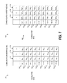
FIG. 7 shows a table 700 having a plurality of cells arranged in a plurality of rows 701-709 and columns 711-713, in accordance with some embodiments.
Each cell in the table 700 contains information, Rx1-Rx27, indicative of the interference that was detected at location 616 with signals supplied to a particular group of conductors. For example, a first cell in the table 700 includes information, Rx1, indicative of the interference (see e.g., waveform 622) that may have been detected at location 616 with signals supplied to the first group of conductors 610 in the communication interface 602. A second cell in the table 700 includes information, Rx2, indicative of the interference that may have been detected at location 616 with signals supplied to the second group of conductors 612 in the communication interface 602. And so on.
FIG. 7 also shows a table 720 having a plurality of cells arranged in a plurality of rows 721-729 and columns 731-733, in accordance with some embodiments.
Each cell in the table 720 contains information, PDP1-PDP27, indicative of a characterization of a channel between the location 616 and a particular group of conductors. For example, a first cell in the table 720 includes information, PDP1, indicative of a characterization of the channel (e.g., channel 624) between the location 616 and the first group of conductors 610 in the communication interface 602. A second cell in the table 700 includes information, PDP2, indicative of a characterization of the channel between the location 616 and the second group of conductors 610 in the communication interface 602. And so on.
In some embodiments, the characterization, e.g., PDP, in each cell of table 720 is generated by applying the transformation 630 to the interference, e.g., Rx, in the corresponding cell in the table 700.
In some embodiments, characterizing a channel between a location and a respective one of the communication interfaces comprises: dividing conductors of the respective one of the communication interface into groups; supplying signals to one of the groups at a time, and for each of the groups, detecting interference that occurs at the location as a result of emissions radiated from the group while the signals are supplied thereto and thereafter characterizing a channel between the location and the group.
In some embodiments, a channel between the location and a group of conductors is characterized by estimating a channel power delay profile (PDP) or other statistical measure of average power or statistical measure of behavior based at least in part on the interference that was detected at the location of interest with the signals supplied to the group.
Referring again to FIG. 4, at 404, the method may further include, for each of the plurality of communication interfaces, supplying signals to the communication interface and detecting interference that occurs at the location as a result of emissions radiated from the plurality of communication interface while the signals are supplied thereto. In some embodiments, the signals are supplied to, and the resulting interference is detected from, one communication interface at a time.
In some embodiments, a different signal is supplied to each conductor in the communication interface. In some embodiments, the signals supplied to the communication interface are signals having low cross correlation properties. In some embodiments, the signals supplied to the communication interface also have autocorrelation properties. In some embodiments, the signals supplied to the communication interface are Gold encoded signals. In some embodiments, the Gold encoded signals may have the characteristics shown in FIG. 8A.
Referring to FIG. 8A, as shown by graphical representation 800, in some embodiments, Gold encoded signals may include a plurality of Gold encoded signals (e.g., represented as Gold code number 1 to 16), each having a high auto correlation (compared with itself) and a low cross correlation (compared each of the others of the plurality of Gold encoded signals). In some embodiments, the plurality of Gold encoded signals may have a uniformly high auto correlation and a uniformly low cross correlation.
In some embodiments, the Gold encoded signals are generated in accordance with FIG. 8B, which shows the structure 850 of the well known maximum length Linear Feedback Shift Register (LFSR) sequences.
Referring to FIG. 8B, maximum length sequences (MLS) are, by definition, the largest codes that can be generated by a given shift register, {ak}, or a delay element of a given LFSR length, K. Typically the connectors of the shift register are described by the coefficients of the polynom, {ck}. Every LFSR sequence shows a periodicity that depends on the length of the LFSR itself as 2K-1. It can be demonstrated that the number of ones and zeros in a MLS is nearly equal and its autocorrelation is Nδ(n), where N is the length of the MLS and δ(•) denotes the Dirac delta function.
The autocorrelation refers to the degree of correspondence between a sequence and a phase-shifted replica of itself. This characteristic autocorrelation is used to great advantage in Spread Spectrum (SS) schemes such as CDMA, and it is of most interest in choosing code sequences that give the least false synchronization probability. With the above characteristics, an MLS is nearly indistinguishable from a pure random code when N is large.
In some embodiments, the cross correlation of two codes is of similar importance. The cross correlation is the measure of agreement between two different codes. The MLS are not immune to cross correlation problems, and they may have large cross correlation values. A lower bound of the cross correlation for the MLS is √{square root over (2K-1)}.
In some embodiments, the goal of SS technique designers is to find a set of spreading codes or waveforms such that many signals as possible can be spread in a band of frequencies such that there is a little mutual interference. Gold Codes are useful because of the larger number of sequences they supply. The Gold codes can be chosen from a set of codes available for a given generator, and their cross correlation is uniform and bounded.
In some embodiments, the Gold codes construction depends on two preferred pair of MLS with length N. Consider that a MLS is denoted by A, and the second MLS is denoted as B. The 2K-1 Gold codes are built by adding the sequence A and the shifted version of B once per time. The cross correlation values for any GC are in the set {−1, 2N−1}, see Fig. X for a 15 bit-long example.
FIG. 9 is a graphical representation 900 showing portion 404 of method 400 with the communication interface 602 and Gold encoded signals, in accordance with some embodiments.
Referring to FIG. 9, in accordance with some embodiments, a different GOLD encoded signal may be supplied to each conductor in the communication interface. Thus, a first signal, i.e., GOLDA or other signal, may be supplied to the first conductor 602 in the communication interface. A second signal, i.e., GOLDB or other signal, may be supplied to the second conductor 604 in the communication interface. A third signal, i.e., GOLDC or other signal, may be supplied to the third conductor 606 in the communication interface. And so on.
The signals may result in interference 914, which may have different characteristics at different locations. The interference may be detected at one or more locations of interest, e.g., location 616. A graph 920 has a waveform 922 representing the interference that may be detected at location 616, in accordance with some embodiments.
Referring again to FIG. 4, at 406, the method may further include, for each of the plurality of communication interfaces, determining an estimate of interference that would occur at the location as a result of emissions radiated from the communication interface while the signals are supplied thereto, based at least in part on the characterization of the channel between the location and the communication interface.
In some embodiments, determining an estimate of interference that would occur at the location as a result of emissions radiated from the communication interface while the signals are supplied thereto, comprises determining a convolution based on information representing the signals supplied to the communication interface (e.g., FIG. 8A) and the characterization of the channel between the location and the communication interfaces (e.g., FIG. 7, table 720, column 731).
Referring again to FIG. 4, at 408, the method may further include, for each of the plurality of communication interfaces, comparing the estimate of interference that would occur at the location to the detected interference that occurs at the location.
In some embodiments, this comprises determining a measure of correlation between the estimate of interference that would occur at the location and the detected interference that occurs at the location. In some embodiments, the measure of correlation may be determined by determining a convolution based on the estimate of interference that would occur at the location and the detected interference that occurs at the location. In some embodiments, the communication interface for which the measure of correlation is greatest will be the communication interface that results in the greatest amount of interference at the location.
At 412, the method may further include identifying a communication interface and/or one or more conductors in the communication interface that result in an undesirable amount of interference at the location of interest. In some embodiments, this may comprise identifying the communication interface for which the measure of correlation between the estimate and the detected interference is greatest. In some embodiments, the communication interface may result in a greatest amount (or at least one of the greatest amounts) of interference at a location of interest. In some embodiments, the communication interface may result in an unacceptable amount of interference at a given location of interest.
In some embodiments, after such source is identified, efforts may be made to mitigate such interference, which may thereby improve system performance in one or more respects. Moreover, if such source can be identified and the interference mitigated, it may be possible to reduce spacing between one or more components within the system, which may make it possible to reduce one or more overall dimension of the system and/or to optimize said system for optimal coexistence of computing and communications subsystems, all within a definable volumetric form (e.g., a mobile device).
At 414, the method may further include modifying a design of one or more systems in response at least in part to the comparison. In some embodiments, this comprises modifying a system that includes one or more integrated circuit package. In some embodiments it comprises modifying one or more of such one or more integrated circuit packages.
In accordance with some embodiments, the interference, the CIR and the channel PDP are time and space dependent and a space-time interference signal identification is feasible as well.
In some embodiments, the system 100 may have more or fewer components than that shown.
In some embodiments, some or all portions of the information described in association with the method 400 is stored in one or more storage devices.
In some embodiments, one or more portions of the method 400 may be performed by a processor.
In some embodiments, a computer-readable storage medium may store thereon instructions that when executed by a processor result in performance of one or more portions of the method 400.
FIG. 10 is a block diagram of an apparatus 1000 according to some embodiments. In some embodiments, the apparatus may be used in identifying a communication interface that results in a greatest amount (or at least one of the greatest amounts), an unacceptable amount and/or merely an undesirable amount of interference at a given location of interest, according to some embodiments.
Referring to FIG. 10, the apparatus may include a characterization unit 1002, a detection unit 1004, an estimation unit 1008 and a comparison unit 1008. In some embodiments, the characterization unit 1002, the detection unit 1004, the estimation unit 1008 and the comparison unit 1008 may perform portions 402, 404, 406 and 408, respectively, of method 400.
The characterization unit 1002 may characterize a plurality of channels, each of the plurality of channels being a channel between a location and a respective one of the plurality of communication interfaces.
In some embodiments, the characterization unit 1002 receives information defining the plurality of communication interfaces, information dividing the conductors of the interfaces into groups, information indicative of signals supplied to one of the groups at a time, and information indicative of detected interference that occurs at the location as a result of emissions radiated from the group while signals are supplied thereto. The characterization unit 1002 may thereafter characterize the plurality of channels based at least in part on the information received thereby.
In some embodiments, the characterization unit 1002 characterizes a channel between the location and a group of conductors by estimating a channel power delay profile (PDP) or other statistical measure of average power or statistical measure of behavior based at least in part on the interference that was detected at the location of interest with the signals supplied to the group.
In some embodiments, each of the groups has a same number of conductors. In some embodiments, the number of conductors in each group is two (sometimes referred to as a pair of conductors).
In some embodiments, the signals are Golay encoded signals. If the number of conductors in a group is equal to two, a first Golay encoded signal may be supplied to a first conductor in the group and a second Golay encoded signals may be supplied to a second conductor in the group. In some embodiments, the Golay encoded signals may have the characteristics shown in FIG. 5, which is a representation of channel sounding characteristics of Golay Complementary Codes, in accordance with some embodiments.
In some embodiments, the characterization unit 1002 may be coupled to a transmitter that transmits the signals that result in the emissions. In some embodiments, the characterization unit 1002 may supply the signals to the transmitter. In some embodiments, the transmitter may be the same as and/or similar to the transmitter 613.
In some embodiments, the characterization unit 1002 may be coupled to ad/or include a detector that detects the interference that occurs at the location as a result of emissions radiated from the group while signals are supplied thereto. In some embodiments, the detector may be the same as and/or similar to the detector 623.
As stated above, In some embodiments, the characterization unit 1002 may characterize a channel by estimating a channel power delay profile (PDP) or other statistical measure of average power or statistical measure of behavior, based at least in part on the interference that was detected at the location of interest with the signals supplied to the group. A graph 626 has a waveform 628 representing an estimated channel power delay profile (PDP), in accordance with one embodiment. In some embodiments, the characterization unit 1002 use a transformation to generate the estimated channel power delay profile (PDP), based at least in part on the interference that was detected at the location of interest with the signals supplied to the group. In some embodiments, the transformation may be the same as and/or similar to the transformation 630.
In some embodiments, the characterization unit 1002 may repeat the above for each group of conductors in the communication interface 602 and each group of conductors in each of the other communication interfaces.
The detection unit 1004 may detect, for each of the plurality of interfaces, interference that occurs at the location as a result of emissions radiated from the communication interface while signals are supplied thereto. In some embodiments, the signals may be supplied to, and interference may be detected from, one of the plurality of communication interfaces at a time.
In some embodiments, the detection unit 1004 may be coupled to a transmitter that transmits the signals that result in the emissions detected by the detection unit 1004. In some embodiments, the detection unit 1004 may supply the signals to the transmitter. In some embodiments, the transmitter may be the same as and/or similar to the transmitter 613.
In some embodiments, the detection unit 1004 may be coupled to and/or include a detector that detects the interference that occurs at the location as a result of emissions radiated from the group while signals are supplied thereto. In some embodiments, the detector may be the same as and/or similar to the detector 623.
In some embodiments, a different signal is supplied to each conductor in the communication interface. In some embodiments, the signals supplied to the communication interface are signals having low cross correlation properties and/or high autocorrelation properties. In some embodiments, the signals supplied to the communication interface are Gold encoded signals. In some embodiments, the Gold encoded signals may have the characteristics shown in FIG. 8A. In some embodiments, the Gold encoded signals are generated in accordance with FIG. 8B.
In some embodiments, the signals may be supplied and the interference may be detected in a manner that is the same as and/or similar to that shown in FIG. 9. For example, in some embodiments, a different GOLD encoded signal may be supplied to each conductor in the communication interface. The signals may result in interference 914, which may have different characteristics at different locations. The interference may be detected at one or more locations of interest, e.g., location 616. A graph 920 has a waveform 922 representing the interference that may be detected at location 616, in accordance with some embodiments.
The estimation unit 1006 may determine, for each of the plurality of communication interfaces, an estimate of interference that would occur at the location as a result of emissions radiated from the communication interface while the signals are supplied thereto.
In some embodiments, the estimation unit 1006 receives information indicative of the signals supplied to the communication interface (e.g., FIG. 8A) and may further receive the characterization of the channel between the location and the communication interfaces (e.g., FIG. 7, table 720, column 731). The estimation unit 1006 may thereafter determine the estimate based at least in part on the information received thereby. In some embodiments, the estimation unit 1006 determines the estimate based on a convolution of the information indicative of the signals supplied to the communication interface (e.g., FIG. 8A) and the characterization of the channel between the location and the communication interfaces (e.g., FIG. 7, table 720, column 731).
The comparison unit 4008 may compare, for each of the plurality of communication interfaces, the estimate of interference that would occur at the location to the detected interference that occurs at the location. In some embodiments, the comparison comprises a determination of a measure of correlation between the estimate of interference that would occur at the location and the detected interference that occurs at the location. In some embodiments, the measure of correlation may be determined by determining a convolution based on the estimate of interference that would occur at the location and the detected interference that occurs at the location.
In some embodiments, the comparison unit 1008 may identify a communication interface and/or one or more conductors in the communication interface that result in an undesirable amount of interference at the location of interest. In some embodiments, this identification may comprise identifying the communication interface for which the measure of correlation between the estimate and the detected interference is greatest. In some embodiments, such communication interface may result in a greatest amount (or at least one of the greatest amounts) of interference at a location of interest and/or an unacceptable amount of interference at a given location of interest.
Although shown separately, in some embodiments, one or more of the characterization unit 1002, the detection unit 1004, the estimation unit 1008 and the comparison unit 1008 may be combined into a single unit.
In some embodiments, some or all portions of the information that is received and/or produced by the characterization unit 1002, the detection unit 1004, the estimation unit 1008 and/or the comparison unit 1008 may be stored in one or more storage devices. In some embodiments, some or all portions of the information that is received and/or produced by the characterization unit 1002, the detection unit 1004, the estimation unit 1008 and/or the comparison unit 1008 may be stored by the characterization unit 1002, the detection unit 1004, the estimation unit 1008 and/or the comparison unit 1008, respectively.
The methods, apparatus, systems computer readable mediums disclosed herein are not limited to use in association with systems such as system 100. Thus, although the system 100 comprises two integrated circuit packages and a circuit board, the methods, apparatus, systems computer readable mediums disclosed herein are not limited to use in association with such type of systems.
FIG. 11 is a block diagram of an architecture 1100 according to some embodiments. In some embodiments, one or more of the systems (or portion(s) thereof) disclosed herein, apparatus (or portion(s) thereof) disclosed herein and/or one or more devices (or portion(s) thereof) disclosed herein may have an architecture that is the same as and/or similar to the architecture 1100 (or portion(s) thereof). In some embodiments, one or more of the methods (or portion(s) thereof) disclosed herein may be performed by system, apparatus and/or devices having an architecture that is the same as and/or similar to the architecture 1100 (or portion(s) thereof).
Referring to FIG. 11, in accordance with some embodiments, the architecture 1100 includes a processor 1101 coupled to a communication device 1102, an input device 1103, an output device 1104 and a storage device 1106.
In some embodiments, the processor 1101 may execute processor-executable program code to provide or otherwise result in one or more portions of one or more functions and/or one or more portions of one or more methods disclosed herein. In some embodiments, the processor 1101 may comprise one or more INTEL® Pentium® processors.
The communication device 1102 may be used to facilitate communication with other devices and/or systems. In some embodiments, communication device 1102 may comprise an Ethernet and/or other type of connection to a network and/or resource and through which apparatus 1100 may receive and/or transmit information.
The input device 1103 may be used to input information. In some embodiments, the input device 1103 may comprise a keyboard, a keypad, a track ball, a touchpad, a mouse or other pointing device, a microphone, a knob or a switch, an infra-red (IR) port and/or a computer media reader.
The output device 1104 may be used to output information. In some embodiments, the output device 1104 may comprise an IR port, a docking station, a display, a speaker and/or a printer.
The storage device 1106 may store one or more programs 1110-1112 and/or other information for operation of the architecture 1100. In some embodiments, the one or more programs and/or other information may include one or more operating systems, one or more database management systems and/or other applications for operation of the architecture 1100. In some embodiments, the one or more programs 1110-1112 may include one or more instructions to be executed by the processor 1101 to provide one or more portions of one or more functions and/or one or more portions of one or more methods disclosed herein. In some embodiments, the one or more programs and/or other information may include one or more databases 1114-1116.
In some embodiments, the storage device 906 may comprise one or more storage devices, such as, for example, magnetic storage devices (e.g., magnetic tape and/or hard disk drives), optical storage devices, and/or semiconductor memory devices such as Random Access Memory (RAM) devices and Read Only Memory (ROM) devices.
In some embodiments, one or more portions of one or more embodiments disclosed herein may be embodied in a system, a method, an apparatus and/or a computer-readable storage medium. A computer-readable storage medium may store thereon instructions that when executed by a processor result in performance of a process according to any of the embodiments described herein.
Unless stated otherwise, a communication interface may comprise any type of communication interface. In some embodiments, one or more of the plurality of communication interfaces is a bus and/or an interconnection (e.g., a wired interconnection). However, in some embodiments, one or more of the communication interfaces is not limited to a bus and/or wired interconnection.
Unless stated otherwise, a location and/or location of interest may comprise any type of location and/or location of interest, respectively. In some embodiments, a location and/or location of interest may be as small as a single point in space. In some other embodiments, a location and/or location of interest may comprise a region and/or region of interest, respectively, that is larger than a single point in space. In some embodiments, a location and/or location of interest may comprise a three dimensional region that is as large as test personnel feel is appropriate and/or may be desired to accomplish a particular objective.
Unless stated otherwise, a processor may comprise any type of processor. For example, a processor may be programmable or non programmable, general purpose or special purpose, dedicated or non dedicated, distributed or non distributed, shared or not shared, and/or any combination thereof. A processor may include, but is not limited to, hardware, software, firmware, and/or any combination thereof. Hardware may include, but is not limited to off the shelf integrated circuits, custom integrated circuits and/or any combination thereof. In some embodiments, a processor comprises a microprocessor. Software may include, but is not limited to, instructions that are storable and/or stored on a computer readable medium, such as, for example, magnetic or optical disk, magnetic or optical tape, CD-ROM, DVD, RAM, EPROM, ROM or other semiconductor memory. A processor may employ continuous signals, periodically sampled signals, and/or any combination thereof. If a processor is distributed, two or more portions of the processor may communicate with one another through a communication link.
In addition, unless stated otherwise, a communication link may be any type of communication link, for example, but not limited to, wired (e.g., conductors, fiber optic cables) or wireless (e.g., acoustic links, electromagnetic links or any combination thereof including, for example, but not limited to microwave links, satellite links, infrared links), and/or combinations thereof, each of which may be public or private, dedicated and/or shared (e.g., a network). A communication link may or may not be a permanent communication link. A communication link may support any type of information in any form, for example, but not limited to, analog and/or digital (e.g., a sequence of binary values, i.e. a bit string) signal(s) in serial and/or in parallel form. The information may or may not be divided into blocks. If divided into blocks, the amount of information in a block may be predetermined or determined dynamically, and/or may be fixed (e.g., uniform) or variable. A communication link may employ a protocol or combination of protocols.
In addition, unless stated otherwise, a “database” may comprise one or more related or unrelated databases.
In addition, unless stated otherwise, data may comprise any type of information and may have and/or be stored in any form. In some embodiments, data may be stored in raw, excerpted, summarized and/or analyzed form.
Unless otherwise stated, terms such as, for example, “in response to” and “based on” mean “in response at least to” and “based at least on”, respectively, so as not to preclude being responsive to and/or based on, more than one thing.
Unless otherwise stated, terms such as, for example, “electrically connected” mean “directly electrically connected” and/or “indirectly electrically connected”.
In addition, unless stated otherwise, terms such as, for example, “comprises”, “has”, “includes”, and all forms thereof, are considered open-ended, so as not to preclude additional elements and/or features. In addition, unless stated otherwise, terms such as, for example, “a”, “one”, “first”, are considered open-ended, and do not mean “only a”, “only one” and “only a first”, respectively. Moreover, unless stated otherwise, the term “first” does not, by itself, require that there also be a “second”.
The several embodiments described herein are solely for the purpose of illustration. Other embodiments may be practiced with modifications and alterations limited only by the claims.

Claims (36)

1. A method comprising:
characterizing a plurality of channels, each of the plurality of channels being a channel between a location and a respective one of the plurality of communication interfaces;
for each of the plurality of communication interfaces, supplying signals to the communication interface and detecting interference that occurs at the location as a result of emissions radiated from the plurality of communication interface while the signals are supplied thereto;
for each of the plurality of communication interfaces, determining an estimate of interference that would occur at the location as a result of emissions radiated from the communication interface while the signals are supplied thereto, based at least in part on the characterization of the channel between the location and the communication interface; and
for each of the plurality of communication interfaces, comparing, using a processor that includes hardware, the estimate of interference that would occur at the location to the detected interference that occurs at the location.
2. The method of claim 1 wherein characterizing a channel between a location and a respective one of the communication interfaces comprises:
dividing conductors of the respective one of the communication interface into groups; and
supplying signals to one of the groups at a time, and for each of the groups, detecting interference that occurs at the location as a result of emissions radiated from the group while the signals are supplied thereto and thereafter characterizing a channel between the location and the group.
3. The method of claim 2 wherein a channel between the location and a group of conductors is characterized by estimating a statistical measure of behavior based at least in part on the interference that was detected at the location of interest with the signals supplied to the group.
4. The method of claim 2 wherein the channel between the location and the group of conductors is characterized by estimating a channel power delay profile based at least in part on the interference that was detected at the location of interest with the signals supplied to the group.
5. The method of claim 2 wherein the signals supplied to the one of the groups at a time are Golay encoded signals.
6. The method of claim 1 wherein the signals are Gold encoded signals.
7. The method of claim 1 wherein determining an estimate of interference that would occur at the location as a result of emissions radiated from the communication interface while the signals are supplied thereto, comprises:
determining a convolution based on information representing the signals supplied to the communication interface and the characterization of the channel between the location and the communication interfaces.
8. The method of claim 1 wherein comparing the estimate of interference that would occur at the location to the detected interference that occurs at the location comprises:
determining a measure of correlation between the estimate of interference that would occur at the location and the detected interference that occurs at the location.
9. The method of claim 1 wherein comparing the estimate of interference that would occur at the location to the detected interference that occurs at the location comprises:
determining a convolution based on the estimate of interference that would occur at the location and the detected interference that occurs at the location.
10. The method of claim 1 further identifying a communication interface that results in an undesired amount of interference at the location based at least in part on the comparison.
11. The method of claim 1 further comprising modifying a design of one or more systems in response at least in part to the comparison.
12. The method of claim 1 further comprising modifying a design of an integrated circuit package in response at least in part to the comparison.
13. The method of claim 1 wherein the processor that includes hardware executes processor-executable program code.
14. The method of claim 1 wherein the characterizing a plurality of channels comprises characterizing the plurality of channels using a processor that includes hardware.
15. The method of claim 1 wherein the determining an estimate of interference comprises determining an estimate of interference using a processor that includes hardware.
16. The method of claim 1 wherein the characterizing a plurality of channels comprises characterizing the plurality of channels using a processor that includes hardware, and wherein the determining an estimate of interference comprises determining an estimate of interference using a processor that includes hardware.
17. A non-transitory computer readable medium storing thereon instructions executable by a processor to result in performance of a method comprising:
characterizing a plurality of channels, each of the plurality of channels being a channel between a location and a respective one of the plurality of communication interfaces;
receiving, for each of the plurality of communication interfaces, information indicative of interference that occurs at the location as a result of emissions radiated from the plurality of communication interface while signals are supplied thereto;
for each of the plurality of communication interfaces, determining an estimate of interference that would occur at the location as a result of emissions radiated from the communication interface while the signals are supplied thereto, based at least in part on the characterization of the channel between the location and the communication interface; and
for each of the plurality of communication interfaces, comparing the estimate of interference that would occur at the location to the detected interference that occurs at the location.
18. The computer readable medium of claim 17 wherein characterizing a channel between a location and a respective one of the communication interfaces comprises:
receiving information dividing conductors of the respective one of the communication interface into groups;
receiving, for each of the groups, information indicative of interference that occurs at the location as a result of emissions radiated from the group while the signals are supplied thereto; and
thereafter characterizing a channel between the location and the group.
19. The computer readable medium of claim 18 wherein a channel between the location and a group of conductors is characterized by estimating a statistical measure of behavior based at least in part on the interference that was detected at the location of interest with the signals supplied to the group.
20. The computer readable medium of claim 18 wherein the channel between the location and the group of conductors is characterized by estimating a channel power delay profile based at least in part on the interference that was detected at the location of interest with the signals supplied to the group.
21. The computer readable medium of claim 18 wherein the signals supplied to the one of the groups at a time are Golay encoded signals.
22. The computer readable medium of claim 17 wherein the signals are Gold encoded signals.
23. The computer readable medium of claim 17 wherein determining an estimate of interference that would occur at the location as a result of emissions radiated from the communication interface while the signals are supplied thereto, comprises:
determining a convolution based on information representing the signals supplied to the communication interface and the characterization of the channel between the location and the communication interfaces.
24. The computer readable medium of claim 17 wherein comparing the estimate of interference that would occur at the location to the detected interference that occurs at the location comprises:
determining a measure of correlation between the estimate of interference that would occur at the location and the detected interference that occurs at the location.
25. The computer readable medium of claim 17 wherein comparing the estimate of interference that would occur at the location to the detected interference that occurs at the location comprises:
determining a convolution based on the estimate of interference that would occur at the location and the detected interference that occurs at the location.
26. The computer readable medium of claim 17 wherein the method further comprises identifying a communication interface that results in an undesired amount of interference at the location based at least in part on the comparison.
27. Apparatus comprising:
a characterization unit to characterize a plurality of channels, each of the plurality of channels being a channel between a location and a respective one of the plurality of communication interfaces;
a unit to receive, for each of the plurality of communication interfaces, information indicative of interference that occurs at the location as a result of emissions radiated from the plurality of communication interface while signals are supplied thereto;
an estimation unit to determine, for each of the plurality of communication interfaces, an estimate of interference that would occur at the location as a result of emissions radiated from the communication interface while the signals are supplied thereto, based at least in part on the characterization of the channel between the location and the communication interface; and
a comparison unit to compare, for each of the plurality of communication interfaces, the estimate of interference that would occur at the location to the detected interference that occurs at the location.
28. The apparatus of claim 27 wherein characterization of a channel between a location and a respective one of the communication interfaces comprises:
receiving information dividing conductors of the respective one of the communication interface into groups; and
receiving, for each of the groups, information indicative of interference that occurs at the location as a result of emissions radiated from the group while the signals are supplied thereto; and
thereafter characterizing a channel between the location and the group.
29. The apparatus of claim 28 wherein a channel between the location and a group of conductors is characterized by estimating a statistical measure of behavior based at least in part on the interference that was detected at the location of interest with the signals supplied to the group.
30. The apparatus of claim 28 wherein the channel between the location and the group of conductors is characterized by estimating a channel power delay profile based at least in part on the interference that was detected at the location of interest with the signals supplied to the group.
31. The apparatus of claim 28 wherein the signals supplied to the one of the groups at a time are Golay encoded signals.
32. The apparatus of claim 27 wherein the signals are Gold encoded signals.
33. The apparatus of claim 27 wherein determination of the estimate of interference that would occur at the location as a result of emissions radiated from the communication interface while the signals are supplied thereto, comprises:
determination of a convolution based on information representing the signals supplied to the communication interface and the characterization of the channel between the location and the communication interfaces.
34. The apparatus of claim 27 wherein comparison of the estimate of interference that would occur at the location to the detected interference that occurs at the location comprises:
determination of a measure of correlation between the estimate of interference that would occur at the location and the detected interference that occurs at the location.
35. The apparatus of claim 27 wherein comparison of the estimate of interference that would occur at the location to the detected interference that occurs at the location comprises:
determination of a convolution based on the estimate of interference that would occur at the location and the detected interference that occurs at the location.
36. The apparatus of claim 27 wherein the comparison unit is further to identify a communication interface that results in an undesired amount of interference at the location based at least in part on the comparison.
US12/823,723 2010-06-25 2010-06-25 Systems, methods, apparatus and computer readable mediums for use in association with systems having interference Expired - Fee Related US8225252B2 (en)

Priority Applications (6)

Application Number Priority Date Filing Date Title
US12/823,723 US8225252B2 (en) 2010-06-25 2010-06-25 Systems, methods, apparatus and computer readable mediums for use in association with systems having interference
CN201180027401.0A CN102918514B (en) 2010-06-25 2011-06-23 The system, method, the equipment that are combined with the noisy system of tool
EP11798933.5A EP2585928B1 (en) 2010-06-25 2011-06-23 Systems, methods, apparatus and computer readable medium for use association with systems having interference
PCT/US2011/041657 WO2011163495A2 (en) 2010-06-25 2011-06-23 Systems, methods, apparatus and computer readable medium for use association with systems having interference
JP2013515586A JP5507758B2 (en) 2010-06-25 2011-06-23 System, method, apparatus, and computer-readable medium used in connection with a system in which interference occurs
KR1020127033455A KR101451613B1 (en) 2010-06-25 2011-06-23 Systems, methods, apparatus and computer readable medium for use association with systems having interference

Applications Claiming Priority (1)

Application Number Priority Date Filing Date Title
US12/823,723 US8225252B2 (en) 2010-06-25 2010-06-25 Systems, methods, apparatus and computer readable mediums for use in association with systems having interference

Publications (2)

Publication Number Publication Date
US20110316561A1 US20110316561A1 (en) 2011-12-29
US8225252B2 true US8225252B2 (en) 2012-07-17

Family

ID=45351938

Family Applications (1)

Application Number Title Priority Date Filing Date
US12/823,723 Expired - Fee Related US8225252B2 (en) 2010-06-25 2010-06-25 Systems, methods, apparatus and computer readable mediums for use in association with systems having interference

Country Status (6)

Country Link
US (1) US8225252B2 (en)
EP (1) EP2585928B1 (en)
JP (1) JP5507758B2 (en)
KR (1) KR101451613B1 (en)
CN (1) CN102918514B (en)
WO (1) WO2011163495A2 (en)

Cited By (1)

* Cited by examiner, † Cited by third party
Publication number Priority date Publication date Assignee Title
US8397191B1 (en) * 2011-11-07 2013-03-12 Xilinx, Inc. Determining failure rate from circuit design layouts

Families Citing this family (10)

* Cited by examiner, † Cited by third party
Publication number Priority date Publication date Assignee Title
US8896295B2 (en) 2012-04-04 2014-11-25 Allegro Microsystems, Llc Magnetic field sensor having multiple sensing elements and a programmable misalignment adjustment device for misalignment detection and correction in current sensing and other applications
US9007054B2 (en) * 2012-04-04 2015-04-14 Allegro Microsystems, Llc Angle sensor with misalignment detection and correction
US9081041B2 (en) 2012-04-04 2015-07-14 Allegro Microsystems, Llc High accuracy differential current sensor for applications like ground fault interrupters
US9806827B2 (en) * 2013-09-13 2017-10-31 Samsung Electronics Co., Ltd. Computing system with interference cancellation mechanism and method of operation thereof
KR20170139680A (en) 2015-04-28 2017-12-19 코닝 인코포레이티드 A method of laser drilling a through hole in a substrate using an exit sacrificial cover layer and a method of laser drilling a through hole
US10410883B2 (en) 2016-06-01 2019-09-10 Corning Incorporated Articles and methods of forming vias in substrates
US10794679B2 (en) 2016-06-29 2020-10-06 Corning Incorporated Method and system for measuring geometric parameters of through holes
US11078112B2 (en) 2017-05-25 2021-08-03 Corning Incorporated Silica-containing substrates with vias having an axially variable sidewall taper and methods for forming the same
US11554984B2 (en) 2018-02-22 2023-01-17 Corning Incorporated Alkali-free borosilicate glasses with low post-HF etch roughness
CN115585753B (en) * 2022-12-13 2023-04-07 中国空气动力研究与发展中心低速空气动力研究所 Optical fiber type icing sensor and method for identifying external appearance of ice

Citations (42)

* Cited by examiner, † Cited by third party
Publication number Priority date Publication date Assignee Title
US5131011A (en) * 1989-06-26 1992-07-14 N. V. Philips' Gloeilampenfabrieken Receiver for data transmission system with nonlinearities
US5799243A (en) 1996-12-30 1998-08-25 Nokia Telecommunications Oy Cellular radio system and a method for measuring the interference level
US5802446A (en) * 1995-03-08 1998-09-01 U.S. Philips Corporation Method and apparatus for testing a communication channel
US6023622A (en) 1997-03-05 2000-02-08 Watkins-Johnson Company Wireless communication system with dynamic channel allocation
US6377065B1 (en) * 2000-04-13 2002-04-23 Advantest Corp. Glitch detection for semiconductor test system
US6385237B1 (en) * 1995-04-27 2002-05-07 Wavetek Wandell And Goltermann Non-invasive digital cable test system
US20020178428A1 (en) * 2001-05-25 2002-11-28 Horne Stephen C. Generation of route rules
US6578421B1 (en) * 1999-12-28 2003-06-17 Fujitsu Limited Acceleration sensor, acceleration sensor device, and method of fabricating an acceleration sensor
US20030145296A1 (en) * 2001-12-19 2003-07-31 Rajit Chandra Formal automated methodology for optimal signal integrity characterization of cell libraries
US6606580B1 (en) * 2000-05-09 2003-08-12 Rolls Royce, Plc Fault diagnosis
US6690739B1 (en) * 2000-01-14 2004-02-10 Shou Yee Mui Method for intersymbol interference compensation
US20040143428A1 (en) * 2003-01-22 2004-07-22 Rappaport Theodore S. System and method for automated placement or configuration of equipment for obtaining desired network performance objectives
US6768729B1 (en) * 1998-09-24 2004-07-27 Nec Corporation CDMA receiver, path detection method, and recording medium on which path detection control program is recorded
US20050127908A1 (en) * 2003-10-10 2005-06-16 Jentek Sensors, Inc. Absolute property measurements using electromagnetic sensors
US20050218908A1 (en) * 2004-04-06 2005-10-06 Alina Deutsch Method to include delta-i noise on chip using lossy transmission line representation for the power mesh
US7013257B1 (en) * 2000-07-21 2006-03-14 Interdigital Technology Corporation Communication transmission impairment emulator
US20060128372A1 (en) * 2004-12-14 2006-06-15 Gazzola James P System and method for coverage analysis in a wireless network
US20060132118A1 (en) * 2004-12-22 2006-06-22 Matsushita Electric Industrial Co., Ltd. Electromagnetic wave analysis apparatus and design support apparatus
US7130776B2 (en) * 2002-03-25 2006-10-31 Lockheed Martin Corporation Method and computer program product for producing a pattern recognition training set
US20070049983A1 (en) 2005-08-29 2007-03-01 Cardiac Pacemakers, Inc. RF telemetry link quality assessment system and method
US20070143719A1 (en) * 2005-12-19 2007-06-21 International Business Machines Corporation Synthesizing current source driver model for analysis of cell characteristics
JP2007155670A (en) * 2005-12-08 2007-06-21 Nec Corp Power source noise resistance inspection circuit, and power source noise resistance inspection method
US7289934B2 (en) * 2005-02-07 2007-10-30 Nec Electronics Corporation Noise measuring system, noise measuring method, and semiconductor device
US20080084953A1 (en) 2006-10-06 2008-04-10 Stmicroelectronics S.R.L. Method and apparatus for suppressing adjacent channel interference and multipath propagation signals and radio receiver using said apparatus
US20080123760A1 (en) * 2006-11-24 2008-05-29 Samsung Electronics Co. Ltd. Interference canceling apparatus and method for use in a broadband wireless communication system
US20080137525A1 (en) * 2006-12-07 2008-06-12 Guanghui Liu Channel estimation method and apparatus determining a channel impulse response (cir) distribution area using two adjacent windows
US20090073440A1 (en) * 2006-09-30 2009-03-19 Timothy Tiemeyer System and method for detecting surface features on a semiconductor workpiece surface
US20090089005A1 (en) * 2007-09-28 2009-04-02 Geoff Hopcraft Generation of test specifications based on measured data points
US20090253898A1 (en) * 2006-04-11 2009-10-08 Engl Heinz W Mathematical Design of ION Channel Selectivity Via Inverse Problem Technology
US20090265593A1 (en) * 2005-11-18 2009-10-22 Panasonic Corporation Method for testing semiconductor integrated circuit and method for verifying design rules
US20090262847A1 (en) * 2008-04-17 2009-10-22 Core Logic, Inc. Orthogonal Frequency Division Multiplexing Receiver for Minimizing Inter-Symbol Interference
US20090281750A1 (en) * 2008-05-07 2009-11-12 Anita Natarajan Method and apparatus for improving noise analysis performance
US20100023909A1 (en) * 2008-07-28 2010-01-28 Fujitsu Limited Voltage fluctuation estimating method and apparatus, semiconductor device operation verification apparatus, semiconductor device designing method, printed circuit board designing method, and program
US20100225466A1 (en) * 2009-03-03 2010-09-09 Synergistic Technology Solutions, Inc. System architecture and apparatus for programmable automatic power supply testing
US20100235134A1 (en) * 2009-03-13 2010-09-16 Kla-Tencor Corporation Methods and systems for generating an inspection process for a wafer
US7805267B2 (en) * 2004-09-22 2010-09-28 Fujitsu Limited Apparatus, method and program for verification of transmission margin
US7865801B2 (en) * 2005-02-17 2011-01-04 Broadcom Corporation Application of a Meta-Viterbi algorithm for communication systems without intersymbol interference
US20110107178A1 (en) * 2008-06-30 2011-05-05 Ehime University Decoder, perpendicular magnetic recording and reproducing device, receiving device, and decoding method
US20110167297A1 (en) * 2010-01-06 2011-07-07 Sun Microsystems, Inc. Clock-data-recovery technique for high-speed links
US20110185262A1 (en) * 2008-07-16 2011-07-28 Daniel Kershaw Error management
US8050843B2 (en) * 2005-03-24 2011-11-01 Abb Research Ltd Estimating health parameters or symptoms of a degrading system
US20110314349A1 (en) * 2006-07-24 2011-12-22 Samsung Electronics Co., Ltd. Data transmitting and receiving system

Family Cites Families (4)

* Cited by examiner, † Cited by third party
Publication number Priority date Publication date Assignee Title
JP2002247119A (en) * 2001-02-20 2002-08-30 Advantest Corp Symbol point estimate device, method, program and recording medium for recording the program and modulation analyzer
WO2004095750A1 (en) * 2003-04-24 2004-11-04 Nec Corporation Channel estimation circuit and channel estimation method
KR101201613B1 (en) * 2004-12-14 2012-11-14 ?란 인코포레이티드 Method and system for reducing signal interference
US20090152740A1 (en) * 2007-12-17 2009-06-18 Soo-San Park Integrated circuit package system with flip chip

Patent Citations (44)

* Cited by examiner, † Cited by third party
Publication number Priority date Publication date Assignee Title
US5131011A (en) * 1989-06-26 1992-07-14 N. V. Philips' Gloeilampenfabrieken Receiver for data transmission system with nonlinearities
US5802446A (en) * 1995-03-08 1998-09-01 U.S. Philips Corporation Method and apparatus for testing a communication channel
US6385237B1 (en) * 1995-04-27 2002-05-07 Wavetek Wandell And Goltermann Non-invasive digital cable test system
US5799243A (en) 1996-12-30 1998-08-25 Nokia Telecommunications Oy Cellular radio system and a method for measuring the interference level
US6023622A (en) 1997-03-05 2000-02-08 Watkins-Johnson Company Wireless communication system with dynamic channel allocation
US6768729B1 (en) * 1998-09-24 2004-07-27 Nec Corporation CDMA receiver, path detection method, and recording medium on which path detection control program is recorded
US6578421B1 (en) * 1999-12-28 2003-06-17 Fujitsu Limited Acceleration sensor, acceleration sensor device, and method of fabricating an acceleration sensor
US6690739B1 (en) * 2000-01-14 2004-02-10 Shou Yee Mui Method for intersymbol interference compensation
US6377065B1 (en) * 2000-04-13 2002-04-23 Advantest Corp. Glitch detection for semiconductor test system
US6606580B1 (en) * 2000-05-09 2003-08-12 Rolls Royce, Plc Fault diagnosis
US7013257B1 (en) * 2000-07-21 2006-03-14 Interdigital Technology Corporation Communication transmission impairment emulator
US20020178428A1 (en) * 2001-05-25 2002-11-28 Horne Stephen C. Generation of route rules
US6732346B2 (en) * 2001-05-25 2004-05-04 Intrinsity, Inc. Generation of route rules
US20030145296A1 (en) * 2001-12-19 2003-07-31 Rajit Chandra Formal automated methodology for optimal signal integrity characterization of cell libraries
US7130776B2 (en) * 2002-03-25 2006-10-31 Lockheed Martin Corporation Method and computer program product for producing a pattern recognition training set
US20040143428A1 (en) * 2003-01-22 2004-07-22 Rappaport Theodore S. System and method for automated placement or configuration of equipment for obtaining desired network performance objectives
US20050127908A1 (en) * 2003-10-10 2005-06-16 Jentek Sensors, Inc. Absolute property measurements using electromagnetic sensors
US20050218908A1 (en) * 2004-04-06 2005-10-06 Alina Deutsch Method to include delta-i noise on chip using lossy transmission line representation for the power mesh
US7805267B2 (en) * 2004-09-22 2010-09-28 Fujitsu Limited Apparatus, method and program for verification of transmission margin
US20060128372A1 (en) * 2004-12-14 2006-06-15 Gazzola James P System and method for coverage analysis in a wireless network
US7642973B2 (en) * 2004-12-22 2010-01-05 Panasonic Corporation Electromagnetic wave analysis apparatus and design support apparatus
US20060132118A1 (en) * 2004-12-22 2006-06-22 Matsushita Electric Industrial Co., Ltd. Electromagnetic wave analysis apparatus and design support apparatus
US7289934B2 (en) * 2005-02-07 2007-10-30 Nec Electronics Corporation Noise measuring system, noise measuring method, and semiconductor device
US7865801B2 (en) * 2005-02-17 2011-01-04 Broadcom Corporation Application of a Meta-Viterbi algorithm for communication systems without intersymbol interference
US8050843B2 (en) * 2005-03-24 2011-11-01 Abb Research Ltd Estimating health parameters or symptoms of a degrading system
US20070049983A1 (en) 2005-08-29 2007-03-01 Cardiac Pacemakers, Inc. RF telemetry link quality assessment system and method
US20090265593A1 (en) * 2005-11-18 2009-10-22 Panasonic Corporation Method for testing semiconductor integrated circuit and method for verifying design rules
JP2007155670A (en) * 2005-12-08 2007-06-21 Nec Corp Power source noise resistance inspection circuit, and power source noise resistance inspection method
US20070143719A1 (en) * 2005-12-19 2007-06-21 International Business Machines Corporation Synthesizing current source driver model for analysis of cell characteristics
US20090253898A1 (en) * 2006-04-11 2009-10-08 Engl Heinz W Mathematical Design of ION Channel Selectivity Via Inverse Problem Technology
US20110314349A1 (en) * 2006-07-24 2011-12-22 Samsung Electronics Co., Ltd. Data transmitting and receiving system
US20090073440A1 (en) * 2006-09-30 2009-03-19 Timothy Tiemeyer System and method for detecting surface features on a semiconductor workpiece surface
US20080084953A1 (en) 2006-10-06 2008-04-10 Stmicroelectronics S.R.L. Method and apparatus for suppressing adjacent channel interference and multipath propagation signals and radio receiver using said apparatus
US20080123760A1 (en) * 2006-11-24 2008-05-29 Samsung Electronics Co. Ltd. Interference canceling apparatus and method for use in a broadband wireless communication system
US20080137525A1 (en) * 2006-12-07 2008-06-12 Guanghui Liu Channel estimation method and apparatus determining a channel impulse response (cir) distribution area using two adjacent windows
US20090089005A1 (en) * 2007-09-28 2009-04-02 Geoff Hopcraft Generation of test specifications based on measured data points
US20090262847A1 (en) * 2008-04-17 2009-10-22 Core Logic, Inc. Orthogonal Frequency Division Multiplexing Receiver for Minimizing Inter-Symbol Interference
US20090281750A1 (en) * 2008-05-07 2009-11-12 Anita Natarajan Method and apparatus for improving noise analysis performance
US20110107178A1 (en) * 2008-06-30 2011-05-05 Ehime University Decoder, perpendicular magnetic recording and reproducing device, receiving device, and decoding method
US20110185262A1 (en) * 2008-07-16 2011-07-28 Daniel Kershaw Error management
US20100023909A1 (en) * 2008-07-28 2010-01-28 Fujitsu Limited Voltage fluctuation estimating method and apparatus, semiconductor device operation verification apparatus, semiconductor device designing method, printed circuit board designing method, and program
US20100225466A1 (en) * 2009-03-03 2010-09-09 Synergistic Technology Solutions, Inc. System architecture and apparatus for programmable automatic power supply testing
US20100235134A1 (en) * 2009-03-13 2010-09-16 Kla-Tencor Corporation Methods and systems for generating an inspection process for a wafer
US20110167297A1 (en) * 2010-01-06 2011-07-07 Sun Microsystems, Inc. Clock-data-recovery technique for high-speed links

Non-Patent Citations (5)

* Cited by examiner, † Cited by third party
Title
"Notification of Transmittal of the International Search Report and the Written Opinion of the International Searching Authority", dated Feb. 17, 2012, for International Application No. PCT/US2011/041657, 10pgs.
Esmael H. Dinan and Bijan Jabbari, "Spreading Codes for Direct Sequence CDMA and Wideband CDMA Cellular Networks", IEEE Communications Magazine, Sep. 1998, (pp. 48-54, 7 pages total).
Marcel J. E. Golay, "Binary Coding", IRE Professional Group on Information Theory, vol. 4, Issue 4, Sep. 1954, (pp. 23-28, 6 pages total).
Marcel J. E. Golay, "Complementary Series", IRE Transactions on Information Theory, vol. 7, Issue 2, Apr. 1961, (pp. 82-87, 6 pages total).
Philip A. Bello, "Characterization of Randomly Time-Variant Linear Channels", IEEE Transactions on Communications Systems, Dec. 1963, (pp. 360-393, 33 pages total).

Cited By (1)

* Cited by examiner, † Cited by third party
Publication number Priority date Publication date Assignee Title
US8397191B1 (en) * 2011-11-07 2013-03-12 Xilinx, Inc. Determining failure rate from circuit design layouts

Also Published As

Publication number Publication date
JP5507758B2 (en) 2014-05-28
KR20130030274A (en) 2013-03-26
EP2585928A4 (en) 2015-10-28
EP2585928A2 (en) 2013-05-01
US20110316561A1 (en) 2011-12-29
WO2011163495A2 (en) 2011-12-29
KR101451613B1 (en) 2014-10-16
CN102918514B (en) 2015-08-26
WO2011163495A3 (en) 2012-04-12
CN102918514A (en) 2013-02-06
JP2013535149A (en) 2013-09-09
EP2585928B1 (en) 2018-08-15

Similar Documents

Publication Publication Date Title
US8225252B2 (en) Systems, methods, apparatus and computer readable mediums for use in association with systems having interference
US10573998B2 (en) Skew-resistant multi-wire channel
Slattery et al. Platform interference in wireless systems: Models, measurement, and mitigation
US7778039B2 (en) Substrates, systems, and devices including structures for suppressing power and ground plane noise, and methods for suppressing power and ground plane noise
KR101594006B1 (en) Chip package connector assembly
JP2016029588A (en) Techniques for locally improving signal to noise in capacitive touch sensor
KR20130069716A (en) Capacitive touch sensor having correlation with a receiver
KR20140010922A (en) Capacitive touch sensor having code-divided and time-divided transmit waveforms
US20230009403A1 (en) Method for antenna calibration and active antenna system for use in antenna calibration
US10383251B1 (en) Heat dissipation structure of electronic device
US10429422B2 (en) EMI testing deviation correction system
Yang et al. Phase Calibration Based Three-Dimensional Beamspace Matrix Pencil Algorithm for Indoor Passive Positioning and Tracking
Hanssens et al. Measurement‐based analysis of specular and dense multipath components at 94 GHz in an indoor environment
Taki et al. Pulse parity modulation for impulse radio UWB transmission based on non-coherent detection
KR101805315B1 (en) Apparatus and Method for implementing Chirp Spread Spectrum using multiple linear chirp
Li et al. EV-sounding: A visual assisted electronic channel sounding system
CN113408234B (en) Integrated circuit chip pin electromagnetic coupling energy estimation method
EP3084894B1 (en) Ground routing device and method
Chung The dual use of power distribution networks for data communications in high speed integrated circuits
US11812560B2 (en) Computer-readable recording medium storing design program, design method, and printed wiring board
Saadaoui et al. IWSN Based on DWPT Using an Industrial Noisy Channel for Industry 4.0 Wireless Applications
Miao et al. Data Transfer Performance Analysis and Enhancement of Critical 3D Interconnects in a 3D SiP Based on Communication Channel Modeling Methodology
Li et al. System‐level SPICE model for predicting the effects of external incident EMI on a shielded communication system with an antenna
Chang et al. Cognitive Bus Coding Scheme for Inter-Chip Communications of Deep Learning Accelerator Chiplet on Low-cost Si and Glass Interposer
Mei et al. Fast Prediction Method for Scattering Parameters of Rigid-Flex PCBs Based on ANN

Legal Events

Date Code Title Description
AS Assignment

Owner name: INTEL CORPORATION, CALIFORNIA

Free format text: ASSIGNMENT OF ASSIGNORS INTEREST;ASSIGNORS:ALCOCER OCHOA, ALBERTO;TINSLEY, KEITH RAYNARD;SIGNING DATES FROM 20100623 TO 20100624;REEL/FRAME:024596/0274

STCF Information on status: patent grant

Free format text: PATENTED CASE

FPAY Fee payment

Year of fee payment: 4

FEPP Fee payment procedure

Free format text: MAINTENANCE FEE REMINDER MAILED (ORIGINAL EVENT CODE: REM.); ENTITY STATUS OF PATENT OWNER: LARGE ENTITY

LAPS Lapse for failure to pay maintenance fees

Free format text: PATENT EXPIRED FOR FAILURE TO PAY MAINTENANCE FEES (ORIGINAL EVENT CODE: EXP.); ENTITY STATUS OF PATENT OWNER: LARGE ENTITY

STCH Information on status: patent discontinuation

Free format text: PATENT EXPIRED DUE TO NONPAYMENT OF MAINTENANCE FEES UNDER 37 CFR 1.362

FP Lapsed due to failure to pay maintenance fee

Effective date: 20200717