US8233301B1 - Impedance dropping dc power supply having an impedance controlled converter - Google Patents
Impedance dropping dc power supply having an impedance controlled converter Download PDFInfo
- Publication number
- US8233301B1 US8233301B1 US12/317,354 US31735408A US8233301B1 US 8233301 B1 US8233301 B1 US 8233301B1 US 31735408 A US31735408 A US 31735408A US 8233301 B1 US8233301 B1 US 8233301B1
- Authority
- US
- United States
- Prior art keywords
- operable
- controller
- switch
- power supply
- converter
- Prior art date
- Legal status (The legal status is an assumption and is not a legal conclusion. Google has not performed a legal analysis and makes no representation as to the accuracy of the status listed.)
- Expired - Fee Related, expires
Links
Images


Classifications
-
- H—ELECTRICITY
- H02—GENERATION; CONVERSION OR DISTRIBUTION OF ELECTRIC POWER
- H02M—APPARATUS FOR CONVERSION BETWEEN AC AND AC, BETWEEN AC AND DC, OR BETWEEN DC AND DC, AND FOR USE WITH MAINS OR SIMILAR POWER SUPPLY SYSTEMS; CONVERSION OF DC OR AC INPUT POWER INTO SURGE OUTPUT POWER; CONTROL OR REGULATION THEREOF
- H02M7/00—Conversion of ac power input into dc power output; Conversion of dc power input into ac power output
- H02M7/02—Conversion of ac power input into dc power output without possibility of reversal
- H02M7/04—Conversion of ac power input into dc power output without possibility of reversal by static converters
- H02M7/12—Conversion of ac power input into dc power output without possibility of reversal by static converters using discharge tubes with control electrode or semiconductor devices with control electrode
- H02M7/21—Conversion of ac power input into dc power output without possibility of reversal by static converters using discharge tubes with control electrode or semiconductor devices with control electrode using devices of a triode or transistor type requiring continuous application of a control signal
- H02M7/217—Conversion of ac power input into dc power output without possibility of reversal by static converters using discharge tubes with control electrode or semiconductor devices with control electrode using devices of a triode or transistor type requiring continuous application of a control signal using semiconductor devices only
Definitions
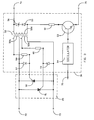
- FIG. 1 is a schematic diagram of an impedance dropping dc power supply 10 having an impedance controlled converter 18 ;
- FIG. 2 is a schematic diagram of the controller 31 seen in FIG. 1 ;
- FIG. 3 is a schematic diagram of the ac switch 25 and driver 30 seen in FIG. 1 ;
- FIG. 4 is a schematic diagram of an alternate embodiment of an impedance dropping dc power supply 10 a having an impedance controlled converter 18 ;
- FIG. 5 is a schematic diagram of a simplified impedance dropping dc power supply 79 ;
- FIG. 6 is a diagrammatic illustration of a fault control device 22 , taken partly in cross-section.
- the power supply 10 may offer one or more of the following advantages.
- It may be compact in size, light in weight, low in cost, stable in operation, and have a long life. It may also have a wide range of ac input voltages.
- the power supply 10 may have a very low power loss (i.e., have a very low heat dissipation), regardless of its ac input voltage, impedance variations of its high impedance device 16 , impedance variations of its load 28 , or the amount of power delivered to its load 28 , thereby helping to improve its efficiency, and extending its operating lifetime and stability of operation by helping to prevent the premature aging, damage, or failure of its various components that might otherwise occur if it dissipated large amounts of heat.
- a very low power loss i.e., have a very low heat dissipation
- the power supply 10 may not need a separate independent dc power supply or a backup battery to support its operations because it draws its power from the ac voltage source 15 , and because of the large capacitors 44 , 45 in its controller 31 .
- the power supply 10 may have a fault control device 22 to help prevent any catastrophic failure of the power supply 10 in the event its TCS (Transient Current Suppression) device 23 , TVS (Transient Voltage Suppression) device 24 , ac switch 25 , or power transformer 26 should fail.
- TCS Transient Current Suppression
- TVS Transient Voltage Suppression
- the Power Supply 10 of FIGS. 1-4 is a diagrammatic representation of the Power Supply 10 of FIGS. 1-4 :
- FIG. 1 Illustrated in FIG. 1 is a schematic diagram of a high voltage impedance dropping dc power supply 10 for converting a high ac input voltage from a high voltage ac source 15 into a low dc output voltage for a load 28 .
- the power supply 10 may comprise any suitable ac input terminals 12 , 13 for receiving a high ac input voltage from the high voltage source 15 ; any suitable high voltage, high impedance input device 16 ; and any suitable impedance controlled converter 18 .
- the term “high voltage” means an ac input voltage that is a minimum of about 600 V ac, up to 100 kV, or more. However, for many applications of the power supply 10 , the high voltage ac source 15 will typically be in the range of from about 4 kV to about 35 kV.
- the power supply 10 is an impedance dropping type of power supply since it has a high voltage, high impedance input device 16 connected in series with the primary winding 26 a of its power transformer 26 .
- An impedance dropping type of power supply 10 may also be called an impedance coupling power supply or a reactive power supply.
- the term “impedance controlled” converter 18 means that the average input impedance of the converter 18 at its input terminals 12 , 20 may be controlled, i.e., may be a function of, the impedance of the load 28 , once the input impedance of the converter 18 at its input terminals 12 , 20 has reached a certain “threshold value”. This “threshold value” will be explained below. The important benefits that may be achieved by using the load 28 's impedance to control the converter 18 's average input impedance will be explained in detail below.
- the high voltage side of the power supply 10 and the converter 18 are those components which are connected, directly or indirectly, to the primary winding 26 a of the transformer 26 , i.e., the high impedance device 16 , the fault control device 22 , the TCS device 23 , the TVS device 24 , and the ac switch 25 .
- the power supply 10 may be designed to receive any of a wide range of high ac input voltages through its input terminals 12 , 13 from any suitable high voltage ac source 15 , such as from a single phase from a power line that may carry from several thousand volts or less, up to one hundred kV, or more.
- the ac source 15 may be connected across the input terminals 12 , 13 in any suitable way, such as by using a hot stick to connect a wire from the power line to one of the input terminals, 12 , 13 ; and by connecting the other input terminal 12 , 13 to ground.
- the power supply 10 may be designed to provide a stable, low voltage dc output voltage that is sufficient to meet the needs of any particular load 28 .
- the load 28 may be a voltage, current, power, or other measuring device that may be used in local, regional or national high voltage electrical power distribution grids.
- the power supply 10 may be designed to provide power to loads 28 having any of a wide range of load impedances, from a few Ohms, or less, up to infinity (an open circuit).
- the High Voltage, High Impedance Input Device 16 The High Voltage, High Impedance Input Device 16 :
- the power supply 10 may comprise any suitable high voltage, high impedance input device 16 , such as one comprising at least one of any suitable: (a) high voltage resistor, (b) high voltage coil, (c) high voltage capacitor, or any suitable combination thereof.
- the functions of the input device 16 may include, for example, helping to control: (a) the ac voltage drop across the primary winding 26 a of the transformer 26 ; (b) the maximum amount of ac current passing though the primary winding 26 a of the power transformer 26 of the converter 18 ; and (c) the maximum continuous current output capacity of the power supply 10 (i.e., the maximum continuous power output capacity of the power supply 10 ).
- the impedance selected for the device 16 will vary depending on such factors as one or more of the above design parameters; and may typically be at least about 500 k ⁇ , although it may be less than this amount.
- the device 16 (capacitors 17 ) had an impedance of about 472.8 k ⁇ .
- the power supply 10 may be perfectly acceptable if any suitable steps that are needed are taken to dissipate the power loss (i.e., the waste heat) generated by the resistor(s) (e.g., thermal isolation, a heat sink, or a cooling fan), in order to prevent any undesirable build up of waste heat in the power supply 10 that may result in the failure of one or more of its components.
- An advantage of using at least one high voltage resistor may be the small size of the resistor(s), which may make the power supply 10 physically smaller as compared to if the input device 16 comprised at least one high voltage coil.
- the input device 16 is selected to comprise at least one of any suitable high voltage coil
- one disadvantage may be the relatively large physical size of the coil(s), which may make the power supply 10 physically larger than if the input device comprised at least one high voltage resistor or at least one high voltage capacitor.
- a power supply 10 may be perfectly acceptable if the physical size of the power supply 10 and dissipating the waste heat generated by the coil(s) are not of concern.
- the power supply 10 may be perfectly acceptable if any suitable steps that are needed are taken to dissipate the waste heat generated by the capacitor(s) 17 (e.g., thermal isolation, heat sinks, or cooling fan).
- the capacitors(s) 17 may be selected to have a relatively small effective series resistance (ESR) in order to reduce the amount of the waste heat generated by the capacitor(s) 17 , so that no additional steps may be needed to dissipate the waste heat generated by the capacitor(s) 17 .
- ESR effective series resistance
- Advantages of using the capacitor(s) 17 may be their small size and the low amount of waste heat that they generate (which may eliminate the need for any waste heat dissipation devices such as thermal isolation, a heat sink, or a cooling fan); and which may make the power supply 10 physically smaller as compared to if the input device 16 comprised high voltage coil(s) or high voltage resistor(s) which needed steps taken to dissipate the waste heat generated by the coil(s) or resistor(s).
- the high impedance device 16 will be treated as comprising at least one high voltage capacitor 17 . If there is more than one high voltage capacitor 17 , then they may be connected together in any suitable series or parallel structure, to provide any desired amount of capacitance at any desired high voltage ac input voltage range for a particular power supply 10 ; it being understood that at least one of any suitable high voltage resistor or at least one of any suitable high voltage coil may be used in lieu of or in addition to, the high voltage capacitor(s) 17 .
- the needed capacitance of the capacitor(s) 17 is a function of the desired maximum continuous current output capacity of the power supply 10 ; and will generally increase as the desired maximum continuous current output capacity of the power supply 10 increases, and vice versa.
- a single input capacitor 17 may be used.
- a series string of input capacitors 17 may also be used because, as is known, when the capacitors 17 are connected in series they will divide the high ac input voltage among themselves in proportion to their respective capacitances, meaning that each capacitor 17 does not have to be rated at the full ac input voltage. For example, if three identical capacitors 17 , each rated at 600V ac, are connected to form a capacitor string, then 1,800V ac may be applied across such a capacitor string. But this comes at the price of reducing the overall capacitance provided by such a capacitor string. However, the overall capacitance of the capacitors 17 may be increased to any desired amount by using two or more strings of capacitors 17 in parallel.
- the converter 18 may comprise on its high voltage side any suitable fault control device 22 , any suitable TCS device 23 , any suitable TVS device 24 , any suitable ac switch 25 , and the primary winding 26 a of any suitable step down power transformer 26 .
- the TVS device 24 and the ac switch 25 may be connected in parallel with the primary winding 26 a of the transformer 26 , to form a parallel network which may be connected in series with the TCS device 23 .
- the fault control device 22 may be connected in parallel with the series connected TCS device 23 and TVS device 24 .
- the fault control device 22 and the high impedance device 16 may be connected in series across the power supply 10 's ac input terminals 12 , 13 .
- the Fault Control Device 22 is :
- the power supply 10 may encounter a self-induced overheating problem due to damage or failure of one or more of its various components, such as its TCS device 23 , TVS device 24 , ac switch 25 , or the primary winding 26 a of its transformer 26 , caused by such things as environmental impacts on the power supply 10 , or by the aging of the affected component.
- damage or failure may increase the affected component's impedance (up to infinity for an affected component that becomes an open circuit), thereby increasing the amount of the input high voltage from the ac source 15 that is dropped across all of the components 23 - 26 .
- this increased ac high voltage is higher than the respective designed operating voltage of one or more of the components 23 - 26 , it may lead to an intermittent or continuous corona discharge across one or more of the components 23 - 26 that heats each of the corona discharge affected components 23 - 26 .
- Such heating may, in turn, cause heating of other components in the power supply 10 , such as the high voltage input capacitors 17 . If unchecked, such heating may eventually cause the failure of other components in the power supply 10 , such as a catastrophic failure of the high voltage input capacitors 17 .
- the fault control device 22 may be selected to be a normally open, temperature controlled fault control device 22 that will automatically permanently close at any predetermined temperature limit, to protect the other components in the power supply 10 by providing a permanent shunt between the ac input connections 11 , 20 of its converter 18 .
- Any suitable electrical, electrical/mechanical, electronic, or electronic/mechanical fault control device 22 that is wired in parallel with the components 23 - 26 may be used that is normally open, but which will automatically and permanently close when it reaches its predetermined high temperature limit.
- the electrical/mechanical fault control device 22 illustrated in FIG. 6 may be used. It may comprise any suitable bimetal member 80 ; any suitable push member 81 ; any suitable conductive switch member 82 ; any suitable holder 83 for members 81 , 82 ; any suitable tensioning member 84 ; any suitable conductors 85 , 86 ; any suitable base 87 ; any suitable releasable holder 88 for the switch member 82 , and any suitable push rod 89 .
- the conductors 85 , 86 may form any suitable switch cavity 90 .
- any suitable bimetal member 80 may be used, such as a bimetal strip 80 or disc 80 .
- a bimetal strip 80 is illustrated in FIG. 6 , it being understood that a person of ordinary skill in the art would be able to easily modify the structure illustrated in FIG. 6 to utilize a bimetal disc 80 instead of a bimetal strip 80 in view of all of the disclosures herein.
- the bimetal strip 80 may be secured to the base 87 , while its free, moveable end may have a push rod 89 secured to it.
- the push rod 89 may have secured to its free end any suitable push member 81 , such as a push ball 81 , for selectively pushing against the switch member 82 .
- the push member 81 may be eliminated, and the push rod 89 may sized so that its free end may selectively push directly against the switch member 82 .
- Any suitable switch member 82 may be used, such as a switch ball 82 .
- the holder 83 may non-conductive and may be sized to receive the push member 81 and the switch member 82 , and may be secured to the conductors 85 , 86 .
- the switch member 82 may be releasably held in the holder 83 by any suitable releasable holder 88 , such as by a pair of spring strips 88 .
- Any suitable tension member 84 such as a tension spring 84 , may extend between the base 87 and the switch member 82 , and may be selected to provide a tension on the switch member 82 throughout the range of motion of the switch member 82 .
- the fault control device 22 illustrated in FIG. 6 is a normally open switch because when the bimetal strip 80 has not reached its predetermined high temperature limit, the switch member 82 is in the position illustrated in FIG. 6 , and the conductors 85 , 86 are not connected together by the switch member 82 .
- the bimetal strip 80 when the bimetal strip 80 reaches its predetermined high temperature limit, the bimetal strip will bend, and cause the push rod 89 and push member 81 to push against the switch member 82 until the switch member 82 is released by its releasable holder 88 .
- the tension member 84 may then pull the switch member 82 into the switch cavity 90 , at which time the switch member 82 will electrically connect the conductors 85 , 86 together.
- the conductors 85 , 86 When the conductors 85 , 86 are electrically connected together, then the ac input terminals 12 , 20 will also be electrically connected together.
- the fault control device 22 may be any suitable electrical, electrical/mechanical, electronic, or electronic/mechanical fault control device 22 that is normally closed (i.e., that is normally conductive), and that is wired in series with the primary winding 26 a of the transformer 26 at a location selected to prevent any of the ac power from the source 15 from reaching the components 23 - 26 once the fault control device 22 has reached its predetermined high temperature limit and has been permanently opened.
- a fault control device 22 may be any suitable thermal fuse that is normally conductive, but that is permanently opened once it reaches its predetermined high temperature limit.
- TCS Transient Current Suppression
- Any suitable TCS device 23 may be used to suppress the flow of a transient current surge though the high impedance device 16 which may be caused, for example, by a high voltage pulse due to a lightening strike on the high voltage power line that acts as the ac source 15 .
- the TCS device 23 may comprise, for example, a small value, non-inductive resistor or resistors in series that may be selected to endure such a high voltage pulse for very short period of time.
- the TCS device has no effect on the normal operation of the power supply 10 when the power supply 10 is not subjected to a transient current surge caused by a high voltage pulse.
- the Transient Voltage Suppression (TVS) Device 24 The Transient Voltage Suppression (TVS) Device 24 :
- Any suitable TVS device 24 may be used such as, for example, any suitable varistor, zener diode, dual zener diode, TVS diode (commonly known as a transorb), or spark gap.
- the functions of the TVS device 24 may include protecting the ac switch 25 and the primary winding 26 a of the transformer 26 from damage that may otherwise be caused by transient voltage peaks such as may be caused, for example, by a lightening strike on the high voltage power line that acts as the ac source 15 .
- the TVS device 24 When the TVS device 24 is activated, it may provide a shunt across the inputs for the ac switch 25 and primary winding 26 a of the transformer 26 .
- the TVS device 24 is triggered it has no effect on the normal operation of the power supply 10 .
- the Ac Switch 25 The Ac Switch 25 :
- any suitable electrical, electrical/mechanical, electronic, or electronic/mechanical ac switch 25 may be wired in parallel with the primary winding 26 a of the transformer 26 to selectively provide a shunt across the primary winding 26 a when it is closed (i.e., when it is on), and to selectively cease to provide that shunt when it is open (i.e., when it is off).
- the ac switch 25 may be operable to selectively prevent and permit a receipt by the rectifier 64 of at least some of the secondary winding ac output current from the secondary winding 26 b of the power transformer 26 by selectively shunting, or not shunting, the primary winding 26 a .
- the ac switch 25 may be operable to periodically open and close as a function of driver control signals it receives from the driver 30 .
- the electronic ac switch 25 illustrated in FIGS. 1 and 3 may be used, which may comprise a pair silicon controlled rectifiers (SCRs) 50 , 51 , also known as thyristors, that are connected in antiparallel, i.e., the two SCRs 50 , 51 are connected in parallel but with their respective polarities reversed.
- SCRs silicon controlled rectifiers
- driver control signals generated by the driver 30 as a function of controller control signals 70 received by the driver 30 from the controller 31 may cause the ac switch 25 to close and open.
- the closing and opening of the ac switch 25 is indirectly controlled by the control signals 70 generated by the controller 31 , since the driver 30 acts as an intermediary between the controller 31 and the ac switch 25 .
- the separate driver 30 may be eliminated, or incorporated as part of the controller 31 , in which the closing and opening of the ac switch 25 may be controlled directly by controller control signals 70 generated by the controller 31 .
- any other suitable electronic ac switch 25 may be used, such as one comprising a triode for alternating current (Triac).
- the Power Transformer 26 The Power Transformer 26 :
- the power transformer 26 's primary winding 26 a may convert a primary winding ac input voltage that it receives from the ac source 15 into a secondary winding ac output current.
- Any suitable power transformer 26 may be used, and may be selected to be a voltage step-down type of transformer 26 so that its turns ratio (i.e., the ratio of the number of turns of its primary winding 26 a to the number of turns of its secondary winding 26 b ) is relatively large, to increase the current passing through its secondary winding 26 b .
- the needed turns ratio of the transformer 26 may be calculated based on the desired maximum continuous current output capacity of the power supply 10 . In general, the needed turns ratio is a function of the desired maximum continuous current output capacity of the power supply 10 , and will increase as the desired maximum continuous current output capacity of the power supply 10 increases, and vice versa.
- the secondary winding 26 b may, or may not, be center-tapped.
- the low voltage side or secondary-side of the converter 18 may comprise the secondary winding 26 b of the transformer 26 ; any suitable rectifier 64 connected in parallel with the secondary winding 26 b ; any suitable driver 30 , any suitable controller 31 , any suitable dc switch 62 , and any suitable regulator 66 connected in parallel with the output of the rectifier 64 ; any suitable diode device 65 connected in series between the positive output end of the rectifier 64 and the controller 31 ; and any suitable input and an output filter capacitors 67 , 68 connected in parallel, respectively, with the input and output ends of the regulator 66 .
- dc power for the various components in the controller 31 and driver 30 may be provided by wires 76 , 77 , 78 to convey dc voltage from the output of the regulator 66 to the driver 30 and the controller 31 .
- the wires 76 , 77 , 78 are not shown in FIGS. 2-3 for clarity, since it would be apparent to any person of ordinary skill in the art how to provide any suitable source of dc power to the various components of the driver 30 and the controller 31 .
- the controller 31 may send controller control signals 70 to the driver 30 and to the dc switch 62 .
- the controller control signals 70 may tell the driver 30 to generate driver control signals to tell the ac switch 25 when to close and open.
- the controller control signals 70 may also tell the dc switch 62 when to close and open.
- the Rectifier 64 and Diode Device 65 are identical to each other.
- a full wave bridge rectifier 64 is illustrated in FIG. 1 .
- any other suitable rectifier 64 may be used that is compatible with the voltage and current handling requirements of the low voltage side of the converter 18 , such as any suitable full wave or half wave rectifier 64 connected in any suitable way to the secondary winding 26 b of the power transformer 26 .
- the secondary winding 26 b may, or may not, be center-tapped.
- Any suitable diode device 65 may be connected in series with the positive output end of the rectifier 64 to prevent a reverse flow of dc current from the controller 31 's high capacitance device 43 to the DC switch 62 when it's closed.
- the DC Switch 62 The DC Switch 62 :
- the dc switch 62 may be operable to selectively permit and prevent a receipt by the controller 31 of at least some of the dc output current from the rectifier 64 .
- the dc switch 62 may be operable to periodically open and close as a function of the controller control signals 70 generated by the controller 31 . While the dc switch 62 is closed, it may be operable to prevent a receipt by the controller 31 of at least some of the dc output current from the rectifier 64 .
- Any suitable electrical, electrical/mechanical, electronic, or electronic/mechanical dc switch 62 may be wired in parallel with the output of the rectifier 64 to selectively provide a shunt across the output of the rectifier 64 when it is closed (i.e., when it is on), and to selectively cease to provide that shunt when it is open (i.e., when it is off).
- the closing and opening of the dc switch 62 may be controlled directly or indirectly by controller control signals 70 generated by the controller 31 .
- the dc switch 62 that is illustrated in FIGS. 1 and 4 is controlled directly by control signals 70 generated by the controller 31 .
- the ac switch 25 may not act as a perfect shunt, in which case a small leakage current may flow through the primary winding 26 a of the transformer 26 which will, in turn, cause a corresponding leakage current to flow through the secondary winding 26 b .
- the leakage current in the secondary winding 26 b may then be rectified by the rectifier 64 and flow to the driver 30 , where it may cause an over voltage failure of the SCRs 50 , 51 in the ac switch 25 . This is because that leakage current may interfere with the holding current and positive voltage triggering mechanism of the SCRs 50 , 51 and prevent them from triggering in time after they receive their respective driver control signals (triggering signals) from the driver 30 .
- any leakage current from the rectifier 64 when the ac switch 25 is closed is shunted by the dc switch 62 , thereby preventing the leakage current from reaching the SCRs 50 , 51 of the ac switch 25 and possibly causing an over voltage failure of the SCRs 50 , 51 .
- the dc switch 62 may be eliminated, such as where more robust SCRs 50 , 51 are used, or where an ac switch 25 is selected to be used that does not permit a leakage current to flow through the primary winding 26 a of the transformer 26 when the driver control signals trigger it to close.
- the Controller 31 The Controller 31 :
- Any suitable controller 31 may be used to generate the control signals 70 for the driver 30 , and for the dc switch 62 as a function of the impedance of the load 28 .
- Any suitable controller 31 may be used, such as the controller 31 illustrated in FIG. 2 , which may comprise any suitable Schmidt trigger circuit 32 , any suitable voltage divider 39 ; any suitable voltage reference 42 ; any suitable high capacitance device 43 ; and any suitable voltage clamping device 49 .
- the voltage clamping device 49 may comprise, for example, any suitable varistor 46 , zener diode 46 , or TVS diode 46 .
- the functions of the voltage clamping device 49 may include protecting the other components of the controller 31 from damage that may otherwise be caused by transient voltage peaks such as may be caused, for example, by a lightening strike on the high voltage power line that acts as the ac source 15 .
- the voltage clamping device 49 When the voltage clamping device 49 is activated, it may keep the voltage across the terminals 74 , 75 clamped. Of course, unless the voltage clamping device 49 is triggered it has no effect on the normal operation of the controller 31 .
- the voltage divider 39 may comprise, for example, a pair of any suitable resistors 40 , 41 .
- the high capacitance device 43 may comprise a single capacitor 44 or 45 ; two or more capacitors 44 , 45 connected in parallel; a single capacitor string that comprises two or more capacitors 44 , 45 that are connected in series; or two or more such capacitor strings that are connected in parallel.
- the discharge rate of the high capacitance device 43 may be at least partially a function of the impedance of the load 28 .
- the functions of the Schmidt trigger circuit 32 may include generating the controller 31 's controller control signals 70 for the driver 30 and for the dc switch 62 as a function of the impedance of the load 28 .
- the frequency of the controller control signals 70 generated by the Schmidt trigger circuit 32 may increase as the impedance of the load 28 decreases, and vice versa.
- the Schmidt trigger circuit 32 may comprise any suitable Schmitt-like trigger circuitry, such as the Schmidt trigger 32 that is illustrated in FIG. 2 , which may comprise any suitable comparator 33 ; a pair of any suitable feedback resistors 34 , 35 ; any suitable voltage divider 36 ; and a pair of any suitable capacitors 47 , 48 .
- the comparator 33 may be connected so as to have positive feedback.
- the capacitors 47 , 48 may be used to suppress high frequency noise, in order to prevent such noise from miss-triggering the Schmidt trigger 32 .
- the voltage divider 36 may comprise, for example, a pair of any suitable resistors 37 , 38 .
- the Schmidt trigger 32 's upper limit voltage may be selected to meet the requirements of not exceeding the rated voltage for the secondary winding 26 b of the power transformer 26 , and of not exceeding the maximum allowed input voltage of the voltage regulator 66 , in order to avoid damage to the transformer 26 and the regulator 66 . Any upper limit voltage may be selected for the Schmidt trigger 32 , as long as that upper limit voltage meets the above requirements.
- the Schmidt trigger 32 's lower limit voltage may be selected to be not less than the minimum allowed input voltage to the regulator 66 , for proper operation of the regulator 66 .
- the lower limit voltage may affect the frequency of the controller control signals 70 that it generates which will, in turn, affect the switching frequency of the ac switch 25 and the dc switch 62 .
- any other suitable Schmidt-like circuitry may be used that performs its needed functions, such as any suitable microcontroller based Schmidt circuitry.
- the Driver 30 The Driver 30 :
- Any suitable driver 30 may be used to generate driver control signals as a function of the controller control signals 70 that the driver 30 may receive from the controller 31 .
- the ac switch 25 may be operable to periodically open and close as a function of the driver control signals it receives from the driver 30 .
- the driver 30 of FIG. 3 may be used, which may comprise a transformer 52 having connected to its primary winding 52 c any suitable dc switch 53 , any suitable oscillator 54 , any suitable resistor 61 , any suitable zener diode 55 , and any suitable diode 56 .
- the driver 30 may further comprise any suitable diode 57 and resistor 58 connected to a first secondary winding 52 a of the transformer 52 , and any suitable diode 59 and any suitable resistor 60 connected to a second secondary winding 52 b of the transformer 52 .
- the transformer 52 may serve the purpose of providing galvanic isolation between the controller 31 and the ac switch 25 , in which case the driver 30 may be a called a galvanic isolation driver 30 .
- the transformer 52 may comprise any suitable transformer such as any suitable pulse transformer 52 having one primary winding 52 c and two secondary windings 52 a , 52 b .
- the two secondary windings 52 a , 52 b of the transformer 52 may be used to separately trigger the gates of SCRs 50 , 51 .
- the primary winding 52 c may be driven by a dc switch 53 and an oscillator 54 that is controlled by the controller control signals 70 that it receives from the controller 31 .
- the resistor 61 may be used to limit the pulse current from the dc switch 53 to the primary winding 52 c of the pulse transformer 52 .
- the diodes 55 , 56 may together form a “snubber”.
- a large voltage spike would be produced in the reverse direction as the primary winding 52 c attempts to keep current flowing in the circuit. This voltage spike is known as an inductive kick.
- Placing the snubber diodes 55 , 56 in parallel with the primary winding 52 c allows the current from the primary winding 52 c to flow through the diodes 55 , 56 , rather than through the switch 53 , thereby protecting the switch 53 from the voltage spike.
- the diodes 57 and 59 may be used to prevent the gates of the SCRs 50 , 51 from reverse gate voltage damage.
- the resistors 58 , 60 may be used to limit the peak gate current of the SCRs 50 , 51 .
- the Voltage Regulator 66 The Voltage Regulator 66 :
- Any suitable voltage regulator 66 may be used to provide any desired output voltage to the load 28 ; and may be, for example, any suitable linear voltage regulator or any suitable switching voltage regulator. Any suitable input and output filter capacitors 67 , 68 may be connected in parallel with, respectively, the input and output of the regulator 66 , to provide any desired filtering for the regulator 66 .
- the high capacitance device 43 of the controller 31 is charged by drawing current from the rectifier 64 , thereby increasing the voltage across the high capacitance device 43 , and causing a corresponding increase in the input voltage to the controller 31 's Schmitt trigger 32 .
- the output voltage of the Schmitt trigger 32 goes from a low level voltage signal to high level voltage signal.
- the high level voltage signal from the Schmitt trigger 32 acts as a high level voltage controller control signal 70 for the driver 30 's oscillator 54 and for the dc switch 62 .
- the high level voltage controller control signal 70 from the Schmitt trigger 32 turns on the driver 30 's oscillator 54 , which then periodically triggers the driver 30 's dc switch 53 .
- the dc switch 53 then provides a periodic pulse train to the primary winding 52 c of the driver 30 's pulse transformer 52 .
- Each of the secondary windings 52 a , 52 b of the pulse transformer 52 then generates a respective periodic pulse train that is sent to its respective SCR 50 , 51 in the ac switch 25 . This causes the SCRs 50 , 51 to switch on (i.e., to close) and shunt the primary winding 26 a of the power transformer 26 .
- the ac switch 25 may be operable to selectively prevent a receipt by the rectifier 64 of at least some of the ac output current from the secondary winding 26 b of the power transformer 26 by shunting the primary winding 26 a and preventing all of the ac input current from entering the primary winding 26 a , aside from a small ac leakage current that may occur due to the nature of the SCRs 50 , 51 . As has been mentioned, this small ac leakage current may then induce a corresponding ac leakage current in the secondary winding 26 b of the transformer 26 which may then cause a corresponding dc leakage current from the rectifier 64 .
- the high level voltage controller control signal 70 from the controller 31 's Schmitt trigger 32 also causes the dc switch 62 to close and shunt any dc leakage current from the rectifier 64 .
- the dc input voltage and dc input power from the rectifier 64 to the driver 30 , controller 31 and regulator 66 are essentially zero. If no dc input power is supplied to the driver 30 , controller 31 , dc switch 62 and regulator 66 , one would normally expect that the power supply 10 would cease functioning and no longer supply power to the load 28 .
- the controller 31 's charged high capacitance device 43 begins to provide electrical energy (dc power) to the voltage regulator 66 that, in turn, continues to provide electrical energy (dc power) to the load 28 .
- the controller 31 's charged high capacitance device 43 also begins to provide electrical energy (dc power) to the ac switch 25 , driver 30 , controller 31 , Schmidt trigger 32 , and dc switch 62 , to maintain all of the power supply 10 's necessary switching operations.
- the high capacitance device 43 is discharged, the voltage across it decreases, thereby decreasing the input voltage to the controller 31 's Schmitt trigger 32 .
- the output voltage signal flips from its high level voltage signal to its low level voltage signal.
- the low level voltage signal from the controller 31 's Schmitt trigger 32 acts as a low level voltage controller control signal 70 for the dc switch 62 and for the driver 30 's oscillator 54 .
- the low level voltage controller control signal 70 causes the dc switch 62 to open and cease shunting the dc current from the output of the rectifier 64 .
- the low level voltage controller control signal 70 from the controller 31 's Schmitt trigger 32 also turns the driver 30 's oscillator 54 off, so that it no longer periodically triggers the driver 30 's dc switch 53 .
- the dc switch 53 then ceases to provide a periodic pulse train to the primary winding 52 c of the driver 30 's pulse transformer 52 .
- the secondary windings 52 a , 52 b cease to generate a periodic pulse train to the ac switch 25 's SCRs 50 , 51 , which causes them to switch off, so that the ac switch 25 no longer shunts the primary winding 26 a of the transformer 26 .
- the rate at which the controller 31 's high capacitance device 43 is charged, and the rate at which is its discharged, may be governed by any applicable factors, such as the impedance of the load 28 , the upper and lower limit voltages of the controller 31 's Schmitt trigger 32 , and the RC (resistor/capacitor) network formed by the controller 31 's high capacitance device 43 and voltage divider 39 .
- the average input impedance of the converter 18 and the maximum output power of the power supply 10 to the load 28 are a function of the impedance of the load 28 and the upper limit voltage of the controller 31 's Schmitt trigger 32 .
- the average input impedance of the converter 18 may be controlled so that it adaptively changes as a function of the impedance of the load 28 .
- the converter 18 may be operable to: (a) adaptively decrease the average input impedance of the converter 18 as the impedance of the load 28 increases, (b) adaptively increase the average input impedance of the converter 18 as the impedance of the load 28 decreases; (c) adaptively decrease the average input power to the converter 18 as the impedance of the load 28 increases, (d) adaptively increase the average input power to the converter 18 as the impedance of the load decreases; (e) adaptively decrease the ac input voltage across the primary winding 26 of the power transformer 26 as the impedance of the load 28 increases; and (f) adaptively increase the ac input voltage across the primary winding 26 as the impedance of the load decreases.
- the converter 18 is operable to keep the ac input voltage across the primary winding 26 a of the power transformer 26 at a voltage that is less than a predetermined maximum voltage, i.e., at a voltage that is less than would otherwise be the case if the power supply 10 did not have a converter 18 .
- the converter 18 may be designed to be operable to keep the ac input voltage across the primary winding 26 a of its power transformer 26 at a voltage which is: (a) less than about 600 V ac, (b) less than about 1 kV ac, (c) less than about 2 kV ac, (c) less than about 1/10 th of the ac input voltage from the ac source 15 across its input terminals 12 , 13 , or (d) in the range of from less than about 1 ⁇ 2 to less than about 1/10 th of the ac input voltage from the ac source 15 across its input terminals 12 , 13 .
- the power supply 10 may then offer the benefits of being smaller in size, lighter in weight, and less in cost than would be the case if the power supply 10 did not have a converter 18 .
- the converter 18 enables the power supply 10 to utilize a power transformer 26 having a primary winding 26 a that has a maximum rated operating voltage that is lower than would be the case if the power supply 10 did not have a converter 18 .
- a power transformer 26 having a primary winding 26 a with a higher maximum rated operating voltage will be larger in size, heavier, and cost more than a power transformer 26 having a primary winding 26 a with a lower maximum rated operating voltage, with the size, weight and cost of the power transformer 26 increasing more and more as the maximum rated operating voltage of its primary winding 26 a increases more and more.
- a power transformer 26 having a primary winding 26 a with a maximum rated operating voltage of 1 kV, or less its size may be on the order of about several inches in each dimension; its weight may be less than about three pounds; and its cost may be less than several tens of dollars.
- a power transformer 26 having a primary winding 26 a with a maximum rated operating voltage of at least 2 kV, such as 14 kV or more its size may be on the order of about several feet in each dimension, or more; its weight may in the range of several tens of pounds to hundreds of pounds, or more; and its cost may be in the range of hundreds of dollars to thousands of dollars, or more.
- Repetition of the power supply 10 's above feedback process results in the average input ac power to the power supply 10 's converter 18 being very close to the average dc power delivered to the load 28 .
- the above example power supply 10 may have the following operating parameters: (a) the input voltage range from the ac source 15 is 8 kV rms to 14 kV rms at 60 cps (cycles per second); (b) the turns ratio of power transformer 26 is 30:1; (c) the secondary side ac current to dc current conversion ratio of the converter 18 , i.e., the ac current to dc current conversion ratio of its rectifier 64 , capacitors 44 , 45 and regulator 66 is 0.9; (d) the maximum continuous output current of power supply 10 to load 28 is 800 mA when ac input voltage is 14 kV, and is 400 mA when ac input voltage is 8 kV; (e) the dc output voltage of power supply 10 to the load 28 is 5 V dc; (f) the maximum continuous power output of the power supply 10 to the load 28 is 4 watts when the ac input voltage is 14 kV, and is 2 watts when the ac
- the various applicable operating parameters of the power supply 10 may be adjusted up, or down, to meet the needs of any particular user of the power supply 10 .
- the power supply 10 's designed maximum continuous dc output current to the load 28 may be selected based on such variables as, for example, the designed maximum dc output voltage to the load 28 and the designed minimum impedance of the load 28 .
- the total capacitance of the input capacitors 17 may be selected based on such variables as, for example, the designed maximum continuous dc output current to the load 28 ; the designed average input impedance range of the converter 18 at its input terminals 12 , 20 once the input impedance of the converter 18 at its input terminals 12 , 20 has reached a certain “threshold value”, the secondary side ac current to dc current conversion ratio of the converter 18 , the turns ratio of the power transformer 26 , the maximum ac input voltage to the terminals 12 , 13 , and the frequency of the ac input voltage to the terminals 12 , 13 .
- an increase in the total capacitance of the input capacitors 17 may result in an increase in the designed maximum continuous dc output current to the load 28 , and vice versa.
- the maximum continuous dc output current to the load 28 (I load ) is selected to be 800 mA
- the input voltage to the terminals 12 , 13 (V input ) is selected to be 14 kV at a frequency (0 of 60 cps
- a simplified estimation of the needed total capacitance of the input capacitors 17 (C) may be done as follows.
- the power supply 10 may have any desired designed range of V input applied to its input terminals 12 , 13 .
- the input capacitors 17 may be arranged in series or in parallel, and their ac voltage ratings may be selected based on the highest desired V input at terminals 12 , 13 .
- the power supply 10 's designed output dc voltage to the load 28 may be obtained by suitably selecting the voltage regulator 66 , which may be, for example, a linear regulator, a switching buck regulator, a switching boost-buck regulator, or a switching boost regulator.
- the voltage regulator 66 may be, for example, a linear regulator, a switching buck regulator, a switching boost-buck regulator, or a switching boost regulator.
- a linear regulator or a switching buck regulator may be a suitable choice.
- a switching boost regulator may be selected.
- the power supply 10 's designed impedance range for the load 28 may be from its lowest rated (allowed) impedance for the load 28 up to an impedance for the load 28 that is infinity (i.e., up to the load 28 being an open circuit).
- the power supply 10 's lowest rated impedance for the load 28 may be selected based on such variables as, for example, the turns ratio of the power transformer 26 (N) and the total capacitance of the input capacitors 17 (C). In general, as N or C is increased, the lowest rated impedance for the load 28 will decrease, and vice versa.
- the input impedance of the converter 18 at its input terminals 12 , 20 will increase as the impedance of the load 28 increases until the input impedance of the converter 18 reaches a “threshold value” that is be determined by the upper limit voltage of the Schmidt trigger 32 in the controller 31 (explained below in more detail).
- any further increase of the impedance of the load 28 will make the average input impedance of the converter 18 at its input terminals 12 , 20 decrease, and vice versa, due to the way the average input impedance of the converter 18 automatically adjusts as a function of the impedance of the load 28 .
- any further increases in the converter 18 's average input impedance at its input terminals 12 , 20 will result in corresponding increases in the ac input voltage across its terminals 12 , 20 , the input power to the converter 18 , and the output power of the converter 18 to the load 28 , and vice versa.
- FIG. 5 Power Supply 79 —Calculation of V primary — winding as a Function of Z load :
- C nominal total capacitance
- FIG. 5 Power Supply 79 —Calculation of V primary — winding as a Function of Z load ,
- V primary — winding may be calculated in the following manner.
- the total impedance of the high voltage capacitors 17 (Z c ) may be calculated as:
- the current that passes through the primary winding 26 a (I primary — winding ) may be calculated as:
- FIG. 1 Power Supply 10 —Calculation of V primary — winding as a Function OF Z load
- FIG. 1 circuit it will now be determined what effect varying the impedance of the load 28 (Z load ) has on the ac input voltage across the primary winding 26 a of the power transformer 26 (V primary — winding ).
- V secondary — winding — max the maximum ac voltage across the secondary winding 26 b of the power transformer 26 (V secondary — winding — max ) will also be 6.5V, since it is approximately equal to the upper limit voltage of the Schmitt trigger 32 .
- V primary — winding may be approximately calculated for various values of Z load as follows.
- the maximum current passing through the converter 18 's input terminals 12 , 20 (I converter — input — max ), may be calculated as:
- V primary — winding — min is the minimum possible voltage across the primary winding 26 a.
- the minimum current passing through the terminals 12 , 20 may be calculated as:
- I converter — input — max and I converter — input — min are essentially constant. This is because in the above equations, V primary — winding — min and V primary — winding — max are essentially negligible as compared to V input .
- the “threshold value” of the impedance of the converter 18 at its input terminals 12 , 20 (Z threshold — value ), i.e., the maximum allowed input impedance of the converter 18 at its input terminals 12 , 20 before the Schmitt trigger 32 will be automatically triggered and the power supply 10 's above feedback process will begin to operate may be calculated as:
- the Schmitt trigger 32 will be automatically triggered and the power supply 10 's above feedback process will begin to operate.
- FIG. 1 Power Supply 10 —Calculation of V primary — winding as a Function of Z load ,
- Z load 20 ⁇ .
- the Schmitt trigger 32 will be automatically triggered and the power supply 10 's above feedback process will begin to operate. If it is also assumed that the dc output voltage of the power supply 10 (V load — dc ) is 5 V, then the power supply 10 's output power to the load (P load ) may be calculated as:
- the dc current to the load 28 (I load — dc ) may be calculated as:
- the secondary side ac to dc transfer ratio of the converter 18 is 0.9. Then the ac current in the secondary winding 26 b of the power transformer 26 (I secondary — winding — ac ) may be calculated as:
- the ac input voltage (rms) across the primary winding 26 a of the power transformer 26 (V primary — winding ) may be calculated as:
- V primary ⁇ ⁇ _ ⁇ ⁇ winding P total ⁇ ⁇ _ ⁇ ⁇ input I converter ⁇ ⁇ _ ⁇ ⁇ input where P total — input is the total input power to the converter 18 .
- P total — input P load +P converter — loss
- P converter — loss P ac — switch — loss +P transformer — loss +P driver — loss +P dc — switch — loss +P rectifier — loss +P diode — loss +P controller/regulator — loss
- P ac — switch — loss , P transformer — loss , P driver — loss , P dc — switch — loss , P rectifier — loss , P diode — loss , and P controller/regulator — loss are the respective power losses of the ac switch 25 , transformer 26 , driver 30 , dc switch 62 , rectifier 64 , diode 65 , and the combination of the controller 31 and regulator 66 .
- the total input power the converter 18 may be calculated as:
- V primary — winding V primary — winding
- FIG. 1 Power Supply 10 and FIG. 5 Power Supply 79 Comparison of Calculations OF V primary — winding as a Function OF Z load
- FIG. 1 power supply 10 and the FIG. 5 power supply 79 are both impedance dropping power supplies because they both utilize a high impedance device 16 in series with the primary winding 26 a of their respective power transformers 26 .
- FIG. 1 POWER FIG. 5 POWER LOAD 28 SUPPLY 10 SUPPLY 79 (Z load ) V primary _winding V primary _winding 20 ⁇ 50 V 532.8 V 200 ⁇ 5.64 V 4,990 V ⁇ ⁇ 0.8 V 14,000 V (Open Circuit) (Full V input across terminals 12, 13)
- the power supply 10 controlled its V primary — winding and maintained it at very low levels (less than 50 V, and actually decreasing as Z load increased), despite a huge variation in Z load from 20 ⁇ to infinity (open circuit).
- a great advantage of the power supply 10 over the power supply 79 is that the power supply 10 may use a power transformer 26 having a low voltage primary winding 26 a , while the power supply 79 is forced to use a power transformer 26 having a high voltage primary winding 26 a , even though both of the power supplies have a V input of 14 kV.
- the power supply 10 may then offer the benefits of being smaller in size, lighter in weight, and less in cost than the power supply 79 since the power supply 10 is able to utilize a power transformer 26 having a primary winding 26 a that has a lower rated maximum operating voltage than would other wise be the case if the power supply 10 did not have a converter 18 .
- FIG. 1 Power Supply 10 —Calculation OF Z converter — input and P converter — loss as a Function OF Z load
- the upper limit voltage of the Schmitt trigger 32 is 6.5 V.
- the maximum ac voltage across the secondary winding 26 b of the power transformer 26 (V secondary — winding — max ) will also be 6.5 V, since it is approximately equal to the upper limit voltage of the Schmitt trigger 32 .
- P converter — loss may be approximately calculated for various value of Z load as follows.
- the maximum current passing through the converter 18 's input terminals 12 , 20 (I converter — input — max ) may be calculated as:
- V primary — winding — min is the minimum possible voltage across the primary winding 26 a.
- Z threshold — value The maximum allowed input impedance of the converter 18 at its input terminals 12 , 20 before the Schmitt trigger 32 will be automatically triggered and the power supply 10 's above feedback process will begin to operate (Z threshold — value ) may be calculated as
- the Schmitt trigger 32 will be automatically triggered and the power supply 10 's above feedback process will begin to operate.
- Z load 20 ⁇ .
- the Schmitt trigger 32 will be automatically triggered and the power supply 10 's above feedback process will begin to operate. If it is also assumed that the dc output voltage of the power supply 10 (V load — dc ) is 5 V, then the power supply 10 's output power to the load (P load ) may be calculated as:
- the dc current to the load 28 (I load — dc ) may be calculated as:
- the secondary side ac to dc transfer ratio of the converter 18 is 0.9. Then the ac current in the secondary winding 26 b of the power transformer 26 (I secondary — winding — ac ) may be calculated as:
- P driver — loss the power loss of the driver 30
- the driver 30 's duty cycle i.e., the on/off ratio of the output signal of its oscillator 54 during the power supply 10 's above feedback process
- P driver — loss 0, since the actual amount of the power loss of the driver 30 is relatively insignificant as compared to the total output power delivered by the secondary winding 26 b of the power transformer 26 .
- V primary — winding V primary — winding
- Z converter — input may be calculated to be 549.1 ⁇
- V primary — winding may be calculated to be 9.28 V
- P converter — input may be calculated to be 156.79 mW
- P load may be calculated to be 125 mW
- P converter — loss may be calculated to be 31.79 mW.
- Z converter — input may be calculated to be 1.69 k ⁇
- V primary — winding may be calculated to be 50 V
- P converter — input may be calculated to be 1.483 W
- P load may be calculated to be 1.25 W
- P converter — loss may be calculated to be 233.8 mW.
- Z converter — input may be calculated to be 190.54 ⁇
- V primary — winding may be calculated to be 5.64 V
- P converter — input may be calculated to be 166.95 mW
- P load may be calculated to be 125 mW
- P converter — loss may be calculated to be 41.95 mW.
- FIG. 1 Power Supply 10 —Summary of Calculations of Z converter — input and P converter — loss as a Function OF Z load
- Z converter input adaptively changed as a function of Z load .
- Z converter input adaptively decreased as Z load increased, regardless of the value for V input .
- P load adaptively changed as a function of Z converter — input .
- P load adaptively decreased as Z converter — input increased.
- the power supply 10 controlled its V primary — winding and maintained it at very low levels of 87.2 V, or less, despite a V input of up to 14 k, and despite a 10-fold increase in Z load from 20 ⁇ , up to 200 ⁇ .
- the importance of the power supply 10 controlling its V primary — winding and maintaining it at very low levels was explained above.
- P converter — loss (the heat dissipated by the converter 18 ), was maintained at very low levels of 223.8 mW, or less, again despite a V input of up to 14 kV, and despite a 10-fold increase in Z load from 20 ⁇ to 200 ⁇ . It may be very important that the converter 18 dissipate as little heat as possible in order to help improve its efficiency, and to help prevent the premature aging, damage, or failure of the various components of the power supply 10 that might otherwise occur if the converter 18 dissipated large amounts of heat.
- the power supply 10 a of FIG. 4 is :
- the power supply 10 a of FIG. 4 is the same as, or at least similar to, the power supply 10 of FIGS. 1-3 in all respects, except for those differences that will be made apparent by all of the disclosures herein. Accordingly, the same reference numerals have been used in FIGS. 1 and 4 for the corresponding parts of the power supplies 10 , 10 a.
- the power supply 10 a may not have the power supply 10 's ac switch 25 , driver 30 , and their associated wiring.
- the power supply 10 a 's dc switch 62 becomes the major component that controls the input power to the controller 31 and to the voltage regulator 66 , and that controls the power supply 10 a 's maximum output power to the load 28 .
- the operation of the power supply 10 a is generally the same as that described above for the power supply 10 , except for the operation of the power supply 10 's ac switch 25 and driver 30 .
- the average input impedance of the power supply 10 a 's converter 18 at its input terminals 12 , 20 adaptively changes as a function of the impedance of the load 28 .
- the average input impedance of the power supply 10 a 's converter 18 adaptively decreases as the impedance of the load 28 increases, and vice versa.
- the output power of the power supply 10 a that is available to the load 28 adaptively changes as a function of the impedance of the load 28 .
- the output power of the power supply 10 a that is available to the load 28 adaptively decreases as the impedance of the load 28 increases, and vice versa.
- Benefits of the power supply 10 a as compared to the power supply 10 are that the power supply 10 a may be less expensive to produce, weigh less, and be more compact that the power supply 10 , since the power supply 10 a does not have the power supply 10 's ac switch 25 , driver 30 , and their associated wiring.
- a detriment of the power supply 10 a may be that it will generate more waste heat than the power supply 10 , due to increased copper loss in the secondary winding 26 b of the transformer 26 and increased power loss in the dc switch 62 , since the power supply 10 a has no ac switch 25 that would enable it to periodically cut off the ac input power to the transformer 26 and dc switch 62 . Nevertheless, in many circumstances, the increased amount of waste heat generated by the power supply 10 a may be easily dissipated, particularly when the input current to the converter 18 is relatively low.
- any particular circuit in the power supply 10 may be suitably combined or formed with one or more of its other circuits, to form one or more larger circuits (e.g., the driver 30 may be made part of the controller 31 ).
- any particular circuit in the power supply 10 may be divided into two or more separate sub-circuits (e.g., the Schmidt trigger 32 in the controller 31 may be made as a circuit which is separate from the controller 31 ), in which case such sub-circuits may be electrically connected together with the other components in the power supply 10 in any suitable way.
Abstract
Description
| REF. | VALUE or | |
| NO. | DEVICE NAME | PART NUMBER/MANUFACTURER |
| 17 | Capacitors | Each is 3,300 pF, 20 kV rms |
| (two in parallel) | ||
| 22 | Fault control | F11090151ZA0060/Cantherm of Montreal, |
| device | Canada | |
| 23 | Resistor | 200 Ω |
| 24 | Transorb | 1V5KE400(C)A/Fairchild Semiconductor of |
| San Jose, Cal. | ||
| 26 | Power | 70060/Amveco Magnetics of Houston, Texas |
| Transformer | ||
| 33 | Comparator, | LMV331/Texas Instruments of Dallas, Texas |
| low voltage | ||
| 34 | Resistor | 100 Ω |
| 35 | Resistor | 300 kΩ |
| 37 | Resistor | 20 kΩ |
| 38 | Resistor | 12.1 kΩ |
| 40, | Resistor | 1 MΩ |
| 41 | ||
| 42 | Voltage reference | LT1790AIS-2.50/Linear Technology of |
| Milpitas, California | ||
| 44, | Capacitors | Each 3.3-4.2 F, 5.5 V dc |
| 45 | (two in series) | |
| 46 | Zener, | 12 V |
| Small Outline | ||
| Diode (SOD) | ||
| package | ||
| 47 | Capacitor | 100 pF |
| 48 | Capacitor | 100 nF |
| 50, | SCR, sensitive | S6010DS2/Littelfuse of Des Plaines, Illinois |
| 51 | gate | |
| 52 | Pulse transformer | TR1_632C/Hammond Manufacturing of |
| Cheektowaga, NY | ||
| 53 | Transistor, control | 2SK2858/NEC of Irving, Texas |
| 54 | Oscillator | ICM7555ID/NXP Semiconductor of |
| Eindhoven, The Netherlands | ||
| 55 | Diode, snub | B240A-13-F/Diodes Incorporated of Dallas, |
| Texas | ||
| 56 | Diode, zener | 12 V |
| 57, | Diode, Schottky | B240A-13-F/Vox Technologies |
| 59 | ||
| 58, | Resistor | 10 Ω |
| 60 | ||
| 61 | Resistor | 400 Ω |
| 62 | Switch, dc | STGB10NB40LZ/STMicroelectronics of |
| (insulated gate, | Geneva, Switzerland | |
| bipolar transistor | ||
| (IGBT)) | ||
| 64 | Rectifier, bridge | Made from diodes # B240A-13-F/Diodes |
| Incorporated of Dallas, Texas (DIODES INC) | ||
| 65 | Diode | B240A-13-F/Diodes Incorporated of Dallas, |
| Texas (DIODES INC) | ||
| 66 | Voltage Regulator | TPS62112/Texas Instruments of Dallas, Texas |
| 67 | Capacitor | 44 μF (ceramic) in parallel with 1,000 μF |
| (aluminum) | ||
| 68 | Capacitor | 66 μF |
Operating Parameters of the Example Power Supply 10:
Z primary
V primary
Case 2 (Vinput=14 kV and Zload=200Ω); and
Case 3 (Vinput=14 kV and Zload=∞Ω (Open Circuit)):
V primary
where Vprimary
Z converter
where Ptotal
P total
where:
P converter
and where Pac
P ac
P ac
P transformer
P dc
P rectifier
P diode
P controller/regulator
As was set forth above:
P converter
Accordingly:
Case 2 (Vinput=14 kV and Zload=20Ω); and
Case 3 (Vinput=14 kV and Zload=∞Ω (Open Circuit)):
| FIG. 1 POWER | FIG. 5 | |
| LOAD | ||
| 28 | |
SUPPLY 79 |
| (Zload) | Vprimary_winding | Vprimary_winding |
| 20 Ω | 50 V | 532.8 V |
| 200 Ω | 5.64 V | 4,990 V |
| ∞ Ω | 0.8 V | 14,000 V |
| (Open Circuit) | (Full Vinput across |
|
V primary
where Vprimary
Z converter
P converter
where Pac
P ac
P ac
P transformer
P dc
P rectifier
P diode
P controller/regulator
As was set forth above:
P converter
Accordingly:
P converter
From the above, the total input power to the converter 23 (Pconverter
P converter
Case 2 (Vinput=8 kV and Zload=20Ω),
Case 3 (Vinput=14 kV and Zload=20Ω), and
Case 4 (Vinput=14 kV and Zload=20Ω):
| Zload | Zconverter_input | Pconverter_input | Pload | Pconverter_loss | Vprimary_winding |
| 20 Ω (Vinput = 8 kV) | 5.16 | kΩ | 1.474 W | 1.25 | W | 223.64 mW | 87.2 V |
| 200 Ω (Vinput = 8 kV) | 549.1 | Ω | 156.79 W | 125 | mW | 31.79 mW | 9.28 |
| 20 Ω (Vinput = 14 kV) | 1.69 | kΩ | 1.483 W | 1.25 | W | 233.8 mW | 50 V |
| 200 Ω (Vinput = 14 kV) | 190.54 | Ω | 166.95 W | 125 | mW | 41.95 mW | 5.64 V |
Claims (39)
Priority Applications (1)
| Application Number | Priority Date | Filing Date | Title |
|---|---|---|---|
| US12/317,354 US8233301B1 (en) | 2008-12-20 | 2008-12-20 | Impedance dropping dc power supply having an impedance controlled converter |
Applications Claiming Priority (1)
| Application Number | Priority Date | Filing Date | Title |
|---|---|---|---|
| US12/317,354 US8233301B1 (en) | 2008-12-20 | 2008-12-20 | Impedance dropping dc power supply having an impedance controlled converter |
Publications (1)
| Publication Number | Publication Date |
|---|---|
| US8233301B1 true US8233301B1 (en) | 2012-07-31 |
Family
ID=46547630
Family Applications (1)
| Application Number | Title | Priority Date | Filing Date |
|---|---|---|---|
| US12/317,354 Expired - Fee Related US8233301B1 (en) | 2008-12-20 | 2008-12-20 | Impedance dropping dc power supply having an impedance controlled converter |
Country Status (1)
| Country | Link |
|---|---|
| US (1) | US8233301B1 (en) |
Cited By (32)
| Publication number | Priority date | Publication date | Assignee | Title |
|---|---|---|---|---|
| US20110140732A1 (en) * | 2009-12-11 | 2011-06-16 | Hong Fu Jin Precision Industry (Shenzhen)Co., Ltd. | Circuit for testing inrush current |
| US20130021700A1 (en) * | 2011-07-21 | 2013-01-24 | Markus Greither | Active clamped transistor circuit |
| WO2013028618A1 (en) * | 2011-08-22 | 2013-02-28 | Franklin Electric Company, Inc. | Power conversion system |
| US20130155743A1 (en) * | 2011-12-20 | 2013-06-20 | Hon Hai Precision Industry Co., Ltd. | Power supply switch apparatus |
| US20130201739A1 (en) * | 2012-02-02 | 2013-08-08 | Engen Technologies Llc | Magnetic flux conversion device |
| US20130329473A1 (en) * | 2012-06-08 | 2013-12-12 | Hon Hai Precision Industry Co., Ltd. | Voltage rectifier |
| US20140043875A1 (en) * | 2012-08-10 | 2014-02-13 | Monolithic Power Systems, Inc. | Off-line regulator and associated method |
| US8724283B1 (en) * | 2010-12-31 | 2014-05-13 | Alpha and Omega, Inc. | A.C. power line surge protectors |
| CN104467082A (en) * | 2014-11-24 | 2015-03-25 | 成都贝发信息技术有限公司 | Power source circuit based on production management system |
| US20170202087A1 (en) * | 2014-07-24 | 2017-07-13 | Siemens Aktiengesellschaft | Electrical power conversion system |
| US9959943B2 (en) | 2007-04-09 | 2018-05-01 | General Electric Company | Method and apparatuses for operating and repairing nuclear reactors |
| US20200186054A1 (en) * | 2012-01-30 | 2020-06-11 | Solaredge Technologies Ltd. | Maximizing Power in a Photovoltaic Distributed Power System |
| US11092632B2 (en) | 2016-10-05 | 2021-08-17 | Hydro-Quebec | Resistance-measuring device and method |
| US11309832B2 (en) | 2006-12-06 | 2022-04-19 | Solaredge Technologies Ltd. | Distributed power harvesting systems using DC power sources |
| US11349432B2 (en) | 2010-11-09 | 2022-05-31 | Solaredge Technologies Ltd. | Arc detection and prevention in a power generation system |
| US11424616B2 (en) | 2008-05-05 | 2022-08-23 | Solaredge Technologies Ltd. | Direct current power combiner |
| US11476799B2 (en) | 2006-12-06 | 2022-10-18 | Solaredge Technologies Ltd. | Distributed power harvesting systems using DC power sources |
| US11489330B2 (en) | 2010-11-09 | 2022-11-01 | Solaredge Technologies Ltd. | Arc detection and prevention in a power generation system |
| US11569659B2 (en) | 2006-12-06 | 2023-01-31 | Solaredge Technologies Ltd. | Distributed power harvesting systems using DC power sources |
| US11569660B2 (en) | 2006-12-06 | 2023-01-31 | Solaredge Technologies Ltd. | Distributed power harvesting systems using DC power sources |
| US11579235B2 (en) | 2006-12-06 | 2023-02-14 | Solaredge Technologies Ltd. | Safety mechanisms, wake up and shutdown methods in distributed power installations |
| US11594968B2 (en) | 2007-08-06 | 2023-02-28 | Solaredge Technologies Ltd. | Digital average input current control in power converter |
| US11598652B2 (en) | 2006-12-06 | 2023-03-07 | Solaredge Technologies Ltd. | Monitoring of distributed power harvesting systems using DC power sources |
| US11620885B2 (en) | 2012-01-30 | 2023-04-04 | Solaredge Technologies Ltd. | Photovoltaic panel circuitry |
| US11682918B2 (en) | 2006-12-06 | 2023-06-20 | Solaredge Technologies Ltd. | Battery power delivery module |
| US11687112B2 (en) | 2006-12-06 | 2023-06-27 | Solaredge Technologies Ltd. | Distributed power harvesting systems using DC power sources |
| US11728768B2 (en) | 2006-12-06 | 2023-08-15 | Solaredge Technologies Ltd. | Pairing of components in a direct current distributed power generation system |
| US11735910B2 (en) | 2006-12-06 | 2023-08-22 | Solaredge Technologies Ltd. | Distributed power system using direct current power sources |
| US11855231B2 (en) | 2006-12-06 | 2023-12-26 | Solaredge Technologies Ltd. | Distributed power harvesting systems using DC power sources |
| US11867729B2 (en) | 2009-05-26 | 2024-01-09 | Solaredge Technologies Ltd. | Theft detection and prevention in a power generation system |
| US11870250B2 (en) | 2016-04-05 | 2024-01-09 | Solaredge Technologies Ltd. | Chain of power devices |
| US11888387B2 (en) | 2006-12-06 | 2024-01-30 | Solaredge Technologies Ltd. | Safety mechanisms, wake up and shutdown methods in distributed power installations |
Citations (55)
| Publication number | Priority date | Publication date | Assignee | Title |
|---|---|---|---|---|
| US4482664A (en) * | 1981-09-29 | 1984-11-13 | Basf Farben & Fasern Ag | Dispersions of finely divided synthetic resins in plasticizers |
| US5055994A (en) | 1989-05-22 | 1991-10-08 | U.S. Phillips Corporation | A.c. to d.c. converter |
| US5341285A (en) | 1992-07-14 | 1994-08-23 | Wave Energy Corporation | Intelligent transformerless system for transferring energy from a power source to an isolated load |
| US5341284A (en) | 1993-06-24 | 1994-08-23 | Hipro Electronics Co., Ltd. | Power-saving power supply unit |
| US5345376A (en) | 1993-02-19 | 1994-09-06 | Tescom Corporation | Switching power supply with electronic isolation |
| US5416387A (en) * | 1993-11-24 | 1995-05-16 | California Institute Of Technology | Single stage, high power factor, gas discharge lamp ballast |
| US5426579A (en) | 1993-07-28 | 1995-06-20 | Best Power Technology, Incorporated | Method and apparatus for stabilizing AC power supply systems connected to power factor correcting loads |
| US5426350A (en) | 1993-11-18 | 1995-06-20 | Electric Power Research Institute, Inc. | High frequency transformerless electronics ballast using double inductor-capacitor resonant power conversion for gas discharge lamps |
| US5442259A (en) | 1994-05-02 | 1995-08-15 | Premark Feg Corporation | Power supply for vacuum fluorescent displays |
| US5469046A (en) | 1993-04-30 | 1995-11-21 | North American Philips Corporation | Transformerless low voltage switching power supply |
| US5499154A (en) | 1994-12-20 | 1996-03-12 | Stewart Electronics | Protective shut-down system for switch-mode power supply |
| US5528686A (en) | 1994-07-08 | 1996-06-18 | At&T Corp. | Transformerless hybrid circuit having direct powered line-side amplifiers |
| US5555494A (en) | 1993-09-13 | 1996-09-10 | Morris; George Q. | Magnetically integrated full wave DC to DC converter |
| US5587629A (en) | 1995-08-28 | 1996-12-24 | Philips Electronics North America Corporation | Transformerless high-voltage generator circuit |
| US5610807A (en) | 1994-10-14 | 1997-03-11 | Matsushita Electric Works, Ltd. | Power converting system with a plurality of charging capacitors |
| US5612580A (en) | 1995-10-10 | 1997-03-18 | Northrop Grumman Corporation | Uninterruptible power system |
| US5646514A (en) | 1993-11-01 | 1997-07-08 | Kabushiki Kaisha Toshiba | AC/DC converter using a non-latch type switching device |
| US5656896A (en) | 1995-02-07 | 1997-08-12 | Sawafuji Electric Co., Ltd. | Power supply for vibrating compressors |
| US5661645A (en) * | 1996-06-27 | 1997-08-26 | Hochstein; Peter A. | Power supply for light emitting diode array |
| US5717320A (en) | 1995-11-27 | 1998-02-10 | U.S. Philips Corporation | Power supply circuit |
| US5729120A (en) | 1996-12-30 | 1998-03-17 | General Signal Corporation | Dynamic voltage regulation stabilization for AC power supply systems |
| US5818708A (en) | 1996-12-12 | 1998-10-06 | Philips Electronics North America Corporation | High-voltage AC to low-voltage DC converter |
| US5886506A (en) | 1996-09-03 | 1999-03-23 | Pioneer Electronic Corporation | Power supply circuit |
| US5892351A (en) | 1997-08-29 | 1999-04-06 | Compaq Computer Corporation | DC-isolated converting battery module |
| US5914869A (en) | 1997-09-15 | 1999-06-22 | General Instrument Corporation | Ac/dc transformerless voltage converter |
| US5986907A (en) | 1996-06-21 | 1999-11-16 | Limpaecher; Rudolf | Method and apparatus for rectification derectification and power flow control |
| US6014325A (en) | 1996-04-15 | 2000-01-11 | Paragon Electric Company, Inc. | Controlled DC power supply for a refrigeration appliance |
| US6057673A (en) | 1998-08-26 | 2000-05-02 | Mitsubishi Denki Kabushiki Kaisha | Compensation device and power transmission system using a compensation device |
| US6061259A (en) * | 1999-08-30 | 2000-05-09 | Demichele; Glenn | Protected transformerless AC to DC power converter |
| US6107886A (en) | 1998-03-31 | 2000-08-22 | Kabushiki Kaisha Toshiba | High-efficiency power amplifier |
| US6175163B1 (en) | 1999-02-16 | 2001-01-16 | Electric Boat Corporation | Integrated high frequency marine power distribution arrangement with transformerless high voltage variable speed drive |
| US6188200B1 (en) | 1997-08-05 | 2001-02-13 | Alternate Energy Concepts, Inc. | Power supply system for sump pump |
| US6198257B1 (en) | 1999-10-01 | 2001-03-06 | Metropolitan Industries, Inc. | Transformerless DC-to-AC power converter and method |
| US6285572B1 (en) | 1999-04-20 | 2001-09-04 | Sanyo Electric Co., Ltd. | Method of operating a power supply system having parallel-connected inverters, and power converting system |
| US6300748B1 (en) | 2000-07-13 | 2001-10-09 | Tyco Electronics Corporation | Transformerless power supply circuit with a switchable capacitive element |
| US20050007082A1 (en) * | 1999-07-07 | 2005-01-13 | Synqor, Inc. | Control of DC/DC converters having synchronous rectifiers |
| US7006366B2 (en) | 2004-06-10 | 2006-02-28 | Wisconsin Alumni Research Foundation | Boost rectifier with half-power rated semiconductor devices |
| US7023176B2 (en) | 2003-06-20 | 2006-04-04 | Uniden Corporation | Transformerless charger with terminal safety features |
| US7079406B2 (en) | 2000-03-29 | 2006-07-18 | Canon Kabushiki Kaisha | Power converting apparatus, control method therefor, and solar power generation apparatus |
| US7088601B2 (en) | 2004-01-23 | 2006-08-08 | Eaton Power Quality Corporation | Power conversion apparatus and methods using DC bus shifting |
| US7102478B2 (en) | 2002-06-21 | 2006-09-05 | Current Technologies, Llc | Power line coupling device and method of using the same |
| US7132819B1 (en) | 2002-11-12 | 2006-11-07 | Current Technologies, Llc | Floating power supply and method of using the same |
| US7176662B2 (en) | 2005-02-23 | 2007-02-13 | Coldwatt, Inc. | Power converter employing a tapped inductor and integrated magnetics and method of operating the same |
| US7200176B1 (en) | 2001-07-06 | 2007-04-03 | Vitesse Semiconductor Corporation | Transformerless ethernet controller |
| US7209373B2 (en) | 2004-12-28 | 2007-04-24 | Kaiser Systems, Inc. | High voltage pulse generator |
| US7212414B2 (en) | 1999-06-21 | 2007-05-01 | Access Business Group International, Llc | Adaptive inductive power supply |
| US7259479B1 (en) | 1999-02-18 | 2007-08-21 | Robertshaw Controls Company | Transformerless power supply, dual positive or dual negative supplies |
| US7262582B2 (en) | 2004-10-14 | 2007-08-28 | Sharp Kabushiki Kaisha | Switching power supply circuit and electronic apparatus provided therewith |
| US7269037B2 (en) | 2002-04-22 | 2007-09-11 | Siemens Aktiengesellschaft | Power supply with a direct converter |
| US7304872B1 (en) | 2004-09-24 | 2007-12-04 | Field Metrics, Inc. | Power supply |
| US7324772B2 (en) | 2005-06-22 | 2008-01-29 | Xerox Corporation | Point-of-load design for high voltage AC power supplies |
| US7359640B2 (en) | 2003-09-30 | 2008-04-15 | Stmicroelectronics Sa | Optical coupling device and method for bidirectional data communication over a common signal line |
| US7371963B2 (en) | 2002-07-31 | 2008-05-13 | Kyocera Corporation | Photovoltaic power generation system |
| US7385375B2 (en) | 2005-02-23 | 2008-06-10 | Coldwatt, Inc. | Control circuit for a depletion mode switch and method of operating the same |
| US7388306B2 (en) | 2001-08-06 | 2008-06-17 | Emerson Electric, Co. | Appliance control system with power controller |
-
2008
- 2008-12-20 US US12/317,354 patent/US8233301B1/en not_active Expired - Fee Related
Patent Citations (56)
| Publication number | Priority date | Publication date | Assignee | Title |
|---|---|---|---|---|
| US4482664A (en) * | 1981-09-29 | 1984-11-13 | Basf Farben & Fasern Ag | Dispersions of finely divided synthetic resins in plasticizers |
| US5055994A (en) | 1989-05-22 | 1991-10-08 | U.S. Phillips Corporation | A.c. to d.c. converter |
| US5341285A (en) | 1992-07-14 | 1994-08-23 | Wave Energy Corporation | Intelligent transformerless system for transferring energy from a power source to an isolated load |
| US5345376A (en) | 1993-02-19 | 1994-09-06 | Tescom Corporation | Switching power supply with electronic isolation |
| US5469046A (en) | 1993-04-30 | 1995-11-21 | North American Philips Corporation | Transformerless low voltage switching power supply |
| US5341284A (en) | 1993-06-24 | 1994-08-23 | Hipro Electronics Co., Ltd. | Power-saving power supply unit |
| US5426579A (en) | 1993-07-28 | 1995-06-20 | Best Power Technology, Incorporated | Method and apparatus for stabilizing AC power supply systems connected to power factor correcting loads |
| US5555494A (en) | 1993-09-13 | 1996-09-10 | Morris; George Q. | Magnetically integrated full wave DC to DC converter |
| US5646514A (en) | 1993-11-01 | 1997-07-08 | Kabushiki Kaisha Toshiba | AC/DC converter using a non-latch type switching device |
| US5426350A (en) | 1993-11-18 | 1995-06-20 | Electric Power Research Institute, Inc. | High frequency transformerless electronics ballast using double inductor-capacitor resonant power conversion for gas discharge lamps |
| US5416387A (en) * | 1993-11-24 | 1995-05-16 | California Institute Of Technology | Single stage, high power factor, gas discharge lamp ballast |
| US5442259A (en) | 1994-05-02 | 1995-08-15 | Premark Feg Corporation | Power supply for vacuum fluorescent displays |
| US5528686A (en) | 1994-07-08 | 1996-06-18 | At&T Corp. | Transformerless hybrid circuit having direct powered line-side amplifiers |
| US5610807A (en) | 1994-10-14 | 1997-03-11 | Matsushita Electric Works, Ltd. | Power converting system with a plurality of charging capacitors |
| US5499154A (en) | 1994-12-20 | 1996-03-12 | Stewart Electronics | Protective shut-down system for switch-mode power supply |
| US5656896A (en) | 1995-02-07 | 1997-08-12 | Sawafuji Electric Co., Ltd. | Power supply for vibrating compressors |
| US5587629A (en) | 1995-08-28 | 1996-12-24 | Philips Electronics North America Corporation | Transformerless high-voltage generator circuit |
| US5612580A (en) | 1995-10-10 | 1997-03-18 | Northrop Grumman Corporation | Uninterruptible power system |
| US5717320A (en) | 1995-11-27 | 1998-02-10 | U.S. Philips Corporation | Power supply circuit |
| US6014325A (en) | 1996-04-15 | 2000-01-11 | Paragon Electric Company, Inc. | Controlled DC power supply for a refrigeration appliance |
| US5986907A (en) | 1996-06-21 | 1999-11-16 | Limpaecher; Rudolf | Method and apparatus for rectification derectification and power flow control |
| US5661645A (en) * | 1996-06-27 | 1997-08-26 | Hochstein; Peter A. | Power supply for light emitting diode array |
| US5886506A (en) | 1996-09-03 | 1999-03-23 | Pioneer Electronic Corporation | Power supply circuit |
| US5818708A (en) | 1996-12-12 | 1998-10-06 | Philips Electronics North America Corporation | High-voltage AC to low-voltage DC converter |
| US5729120A (en) | 1996-12-30 | 1998-03-17 | General Signal Corporation | Dynamic voltage regulation stabilization for AC power supply systems |
| US6188200B1 (en) | 1997-08-05 | 2001-02-13 | Alternate Energy Concepts, Inc. | Power supply system for sump pump |
| US5892351A (en) | 1997-08-29 | 1999-04-06 | Compaq Computer Corporation | DC-isolated converting battery module |
| US5914869A (en) | 1997-09-15 | 1999-06-22 | General Instrument Corporation | Ac/dc transformerless voltage converter |
| US6107886A (en) | 1998-03-31 | 2000-08-22 | Kabushiki Kaisha Toshiba | High-efficiency power amplifier |
| US6057673A (en) | 1998-08-26 | 2000-05-02 | Mitsubishi Denki Kabushiki Kaisha | Compensation device and power transmission system using a compensation device |
| US6175163B1 (en) | 1999-02-16 | 2001-01-16 | Electric Boat Corporation | Integrated high frequency marine power distribution arrangement with transformerless high voltage variable speed drive |
| US7259479B1 (en) | 1999-02-18 | 2007-08-21 | Robertshaw Controls Company | Transformerless power supply, dual positive or dual negative supplies |
| US6285572B1 (en) | 1999-04-20 | 2001-09-04 | Sanyo Electric Co., Ltd. | Method of operating a power supply system having parallel-connected inverters, and power converting system |
| US7212414B2 (en) | 1999-06-21 | 2007-05-01 | Access Business Group International, Llc | Adaptive inductive power supply |
| US20050007082A1 (en) * | 1999-07-07 | 2005-01-13 | Synqor, Inc. | Control of DC/DC converters having synchronous rectifiers |
| US6061259A (en) * | 1999-08-30 | 2000-05-09 | Demichele; Glenn | Protected transformerless AC to DC power converter |
| US6198257B1 (en) | 1999-10-01 | 2001-03-06 | Metropolitan Industries, Inc. | Transformerless DC-to-AC power converter and method |
| US7079406B2 (en) | 2000-03-29 | 2006-07-18 | Canon Kabushiki Kaisha | Power converting apparatus, control method therefor, and solar power generation apparatus |
| US6300748B1 (en) | 2000-07-13 | 2001-10-09 | Tyco Electronics Corporation | Transformerless power supply circuit with a switchable capacitive element |
| US7200176B1 (en) | 2001-07-06 | 2007-04-03 | Vitesse Semiconductor Corporation | Transformerless ethernet controller |
| US7388306B2 (en) | 2001-08-06 | 2008-06-17 | Emerson Electric, Co. | Appliance control system with power controller |
| US7269037B2 (en) | 2002-04-22 | 2007-09-11 | Siemens Aktiengesellschaft | Power supply with a direct converter |
| US7102478B2 (en) | 2002-06-21 | 2006-09-05 | Current Technologies, Llc | Power line coupling device and method of using the same |
| US7371963B2 (en) | 2002-07-31 | 2008-05-13 | Kyocera Corporation | Photovoltaic power generation system |
| US7132819B1 (en) | 2002-11-12 | 2006-11-07 | Current Technologies, Llc | Floating power supply and method of using the same |
| US7023176B2 (en) | 2003-06-20 | 2006-04-04 | Uniden Corporation | Transformerless charger with terminal safety features |
| US7359640B2 (en) | 2003-09-30 | 2008-04-15 | Stmicroelectronics Sa | Optical coupling device and method for bidirectional data communication over a common signal line |
| US7088601B2 (en) | 2004-01-23 | 2006-08-08 | Eaton Power Quality Corporation | Power conversion apparatus and methods using DC bus shifting |
| US7006366B2 (en) | 2004-06-10 | 2006-02-28 | Wisconsin Alumni Research Foundation | Boost rectifier with half-power rated semiconductor devices |
| US7304872B1 (en) | 2004-09-24 | 2007-12-04 | Field Metrics, Inc. | Power supply |
| US7262582B2 (en) | 2004-10-14 | 2007-08-28 | Sharp Kabushiki Kaisha | Switching power supply circuit and electronic apparatus provided therewith |
| US7209373B2 (en) | 2004-12-28 | 2007-04-24 | Kaiser Systems, Inc. | High voltage pulse generator |
| US7298118B2 (en) | 2005-02-23 | 2007-11-20 | Coldwatt, Inc. | Power converter employing a tapped inductor and integrated magnetics and method of operating the same |
| US7385375B2 (en) | 2005-02-23 | 2008-06-10 | Coldwatt, Inc. | Control circuit for a depletion mode switch and method of operating the same |
| US7176662B2 (en) | 2005-02-23 | 2007-02-13 | Coldwatt, Inc. | Power converter employing a tapped inductor and integrated magnetics and method of operating the same |
| US7324772B2 (en) | 2005-06-22 | 2008-01-29 | Xerox Corporation | Point-of-load design for high voltage AC power supplies |
Cited By (48)
| Publication number | Priority date | Publication date | Assignee | Title |
|---|---|---|---|---|
| US11594882B2 (en) | 2006-12-06 | 2023-02-28 | Solaredge Technologies Ltd. | Distributed power harvesting systems using DC power sources |
| US11569659B2 (en) | 2006-12-06 | 2023-01-31 | Solaredge Technologies Ltd. | Distributed power harvesting systems using DC power sources |
| US11855231B2 (en) | 2006-12-06 | 2023-12-26 | Solaredge Technologies Ltd. | Distributed power harvesting systems using DC power sources |
| US11735910B2 (en) | 2006-12-06 | 2023-08-22 | Solaredge Technologies Ltd. | Distributed power system using direct current power sources |
| US11728768B2 (en) | 2006-12-06 | 2023-08-15 | Solaredge Technologies Ltd. | Pairing of components in a direct current distributed power generation system |
| US11687112B2 (en) | 2006-12-06 | 2023-06-27 | Solaredge Technologies Ltd. | Distributed power harvesting systems using DC power sources |
| US11682918B2 (en) | 2006-12-06 | 2023-06-20 | Solaredge Technologies Ltd. | Battery power delivery module |
| US11309832B2 (en) | 2006-12-06 | 2022-04-19 | Solaredge Technologies Ltd. | Distributed power harvesting systems using DC power sources |
| US11476799B2 (en) | 2006-12-06 | 2022-10-18 | Solaredge Technologies Ltd. | Distributed power harvesting systems using DC power sources |
| US11888387B2 (en) | 2006-12-06 | 2024-01-30 | Solaredge Technologies Ltd. | Safety mechanisms, wake up and shutdown methods in distributed power installations |
| US11658482B2 (en) | 2006-12-06 | 2023-05-23 | Solaredge Technologies Ltd. | Distributed power harvesting systems using DC power sources |
| US11594881B2 (en) | 2006-12-06 | 2023-02-28 | Solaredge Technologies Ltd. | Distributed power harvesting systems using DC power sources |
| US11594880B2 (en) | 2006-12-06 | 2023-02-28 | Solaredge Technologies Ltd. | Distributed power harvesting systems using DC power sources |
| US11579235B2 (en) | 2006-12-06 | 2023-02-14 | Solaredge Technologies Ltd. | Safety mechanisms, wake up and shutdown methods in distributed power installations |
| US11575260B2 (en) | 2006-12-06 | 2023-02-07 | Solaredge Technologies Ltd. | Distributed power harvesting systems using DC power sources |
| US11575261B2 (en) | 2006-12-06 | 2023-02-07 | Solaredge Technologies Ltd. | Distributed power harvesting systems using DC power sources |
| US11569660B2 (en) | 2006-12-06 | 2023-01-31 | Solaredge Technologies Ltd. | Distributed power harvesting systems using DC power sources |
| US11598652B2 (en) | 2006-12-06 | 2023-03-07 | Solaredge Technologies Ltd. | Monitoring of distributed power harvesting systems using DC power sources |
| US9959943B2 (en) | 2007-04-09 | 2018-05-01 | General Electric Company | Method and apparatuses for operating and repairing nuclear reactors |
| US11594968B2 (en) | 2007-08-06 | 2023-02-28 | Solaredge Technologies Ltd. | Digital average input current control in power converter |
| US11424616B2 (en) | 2008-05-05 | 2022-08-23 | Solaredge Technologies Ltd. | Direct current power combiner |
| US11867729B2 (en) | 2009-05-26 | 2024-01-09 | Solaredge Technologies Ltd. | Theft detection and prevention in a power generation system |
| US20110140732A1 (en) * | 2009-12-11 | 2011-06-16 | Hong Fu Jin Precision Industry (Shenzhen)Co., Ltd. | Circuit for testing inrush current |
| US8319516B2 (en) * | 2009-12-11 | 2012-11-27 | Hong Fu Jin Precision Industry (Shenzhen) Co., Ltd. | Circuit for testing inrush current |
| US11489330B2 (en) | 2010-11-09 | 2022-11-01 | Solaredge Technologies Ltd. | Arc detection and prevention in a power generation system |
| US11349432B2 (en) | 2010-11-09 | 2022-05-31 | Solaredge Technologies Ltd. | Arc detection and prevention in a power generation system |
| US8724283B1 (en) * | 2010-12-31 | 2014-05-13 | Alpha and Omega, Inc. | A.C. power line surge protectors |
| US20130021700A1 (en) * | 2011-07-21 | 2013-01-24 | Markus Greither | Active clamped transistor circuit |
| EP2748916A4 (en) * | 2011-08-22 | 2015-03-04 | Franklin Electric Co Inc | Power conversion system |
| WO2013028618A1 (en) * | 2011-08-22 | 2013-02-28 | Franklin Electric Company, Inc. | Power conversion system |
| US9479070B2 (en) | 2011-08-22 | 2016-10-25 | Franklin Electric Co., Inc. | Power conversion system |
| CN103176492B (en) * | 2011-12-20 | 2015-07-01 | 中山市云创知识产权服务有限公司 | Power supply automatic gear-shift device |
| US8837180B2 (en) * | 2011-12-20 | 2014-09-16 | Hong Fu Jin Precision Industry (Wuhan) Co., Ltd. | Power supply switch apparatus |
| US20130155743A1 (en) * | 2011-12-20 | 2013-06-20 | Hon Hai Precision Industry Co., Ltd. | Power supply switch apparatus |
| CN103176492A (en) * | 2011-12-20 | 2013-06-26 | 鸿富锦精密工业(武汉)有限公司 | Power supply automatic gear-shift device |
| US20200186054A1 (en) * | 2012-01-30 | 2020-06-11 | Solaredge Technologies Ltd. | Maximizing Power in a Photovoltaic Distributed Power System |
| US11929620B2 (en) * | 2012-01-30 | 2024-03-12 | Solaredge Technologies Ltd. | Maximizing power in a photovoltaic distributed power system |
| US11620885B2 (en) | 2012-01-30 | 2023-04-04 | Solaredge Technologies Ltd. | Photovoltaic panel circuitry |
| US9042136B2 (en) * | 2012-02-02 | 2015-05-26 | Engen Technologies Llc | Magnetic flux conversion device |
| US20130201739A1 (en) * | 2012-02-02 | 2013-08-08 | Engen Technologies Llc | Magnetic flux conversion device |
| US20130329473A1 (en) * | 2012-06-08 | 2013-12-12 | Hon Hai Precision Industry Co., Ltd. | Voltage rectifier |
| US8917076B2 (en) * | 2012-08-10 | 2014-12-23 | Monolithic Power Systems, Inc. | Off-line regulator with pass device and associated method |
| US20140043875A1 (en) * | 2012-08-10 | 2014-02-13 | Monolithic Power Systems, Inc. | Off-line regulator and associated method |
| US20170202087A1 (en) * | 2014-07-24 | 2017-07-13 | Siemens Aktiengesellschaft | Electrical power conversion system |
| US10091885B2 (en) * | 2014-07-24 | 2018-10-02 | Siemens Aktiengesellschaft | Electrical power conversion system |
| CN104467082A (en) * | 2014-11-24 | 2015-03-25 | 成都贝发信息技术有限公司 | Power source circuit based on production management system |
| US11870250B2 (en) | 2016-04-05 | 2024-01-09 | Solaredge Technologies Ltd. | Chain of power devices |
| US11092632B2 (en) | 2016-10-05 | 2021-08-17 | Hydro-Quebec | Resistance-measuring device and method |
Similar Documents
| Publication | Publication Date | Title |
|---|---|---|
| US8233301B1 (en) | Impedance dropping dc power supply having an impedance controlled converter | |
| KR102389241B1 (en) | Electronic switches and dimmers | |
| US6714429B2 (en) | Active inrush current control for AC to DC converters | |
| US9572224B2 (en) | Bleeder protection using thermal foldback | |
| US20060274468A1 (en) | Active inrush current control using a relay for AC to DC converters | |
| KR20190067907A (en) | High efficiency AC-DC extraction converter and method | |
| US8928235B2 (en) | Damper circuit for switched dimming | |
| US20160218626A1 (en) | Damper circuit for switched dimming | |
| ES2781108T3 (en) | Power supply device and procedure for limiting the output current of the power supply device | |
| RU2642839C2 (en) | High-voltage dc-to-dc converter | |
| US6493245B1 (en) | Inrush current control for AC to DC converters | |
| JP2009213345A (en) | Overcurrent protective device of variable-speed drive device | |
| JP2011198739A (en) | Reduced flicker ac led lamp with separately shortable section of led string | |
| JP2008022698A (en) | Method and arrangement of high voltage power supply circuit | |
| KR20040050922A (en) | Frequency modulated self-oscillating switching power supply | |
| US20030111910A1 (en) | Voltage sag and over-voltage compensation device with pulse-width modulated transformer | |
| EP2765696A1 (en) | Switching power supply circuit with protective function | |
| CN100405729C (en) | Power supply with surge voltage control functions | |
| EP2051359A1 (en) | Power supply circuit and earth leakage circuit breaker using the same | |
| JPH1197747A (en) | Lighting circuit for ac light emitting diode | |
| CA2692122C (en) | Microcontroller operated current limited switching power supply for circuit protective devices | |
| JP6512507B2 (en) | Lighting device, lighting device and lighting device | |
| US7463473B2 (en) | Resonance field discharge | |
| DK180187B1 (en) | Overvoltage protection circuit | |
| CN113396540A (en) | Switching device for breaking a current path |
Legal Events
| Date | Code | Title | Description |
|---|---|---|---|
| AS | Assignment |
Owner name: SENSORLINK CORPORATION, WASHINGTON Free format text: ASSIGNMENT OF ASSIGNORS INTEREST;ASSIGNOR:GUO, ZHIJIANG, MR.;REEL/FRAME:022384/0473 Effective date: 20081215 |
|
| STCF | Information on status: patent grant |
Free format text: PATENTED CASE |
|
| FPAY | Fee payment |
Year of fee payment: 4 |
|
| FEPP | Fee payment procedure |
Free format text: MAINTENANCE FEE REMINDER MAILED (ORIGINAL EVENT CODE: REM.); ENTITY STATUS OF PATENT OWNER: SMALL ENTITY |
|
| LAPS | Lapse for failure to pay maintenance fees |
Free format text: PATENT EXPIRED FOR FAILURE TO PAY MAINTENANCE FEES (ORIGINAL EVENT CODE: EXP.); ENTITY STATUS OF PATENT OWNER: SMALL ENTITY |
|
| STCH | Information on status: patent discontinuation |
Free format text: PATENT EXPIRED DUE TO NONPAYMENT OF MAINTENANCE FEES UNDER 37 CFR 1.362 |