US8245094B2 - Rank modulation for flash memories - Google Patents
Rank modulation for flash memories Download PDFInfo
- Publication number
- US8245094B2 US8245094B2 US12/275,186 US27518608A US8245094B2 US 8245094 B2 US8245094 B2 US 8245094B2 US 27518608 A US27518608 A US 27518608A US 8245094 B2 US8245094 B2 US 8245094B2
- Authority
- US
- United States
- Prior art keywords
- permutation
- data
- values
- code
- cell
- Prior art date
- Legal status (The legal status is an assumption and is not a legal conclusion. Google has not performed a legal analysis and makes no representation as to the accuracy of the status listed.)
- Active, expires
Links
- 230000015654 memory Effects 0.000 title claims abstract description 115
- 238000000034 method Methods 0.000 claims description 82
- 230000006870 function Effects 0.000 claims description 79
- 230000007704 transition Effects 0.000 claims description 69
- 238000013500 data storage Methods 0.000 claims description 61
- 125000004122 cyclic group Chemical group 0.000 claims description 37
- 238000004891 communication Methods 0.000 claims description 13
- 238000013507 mapping Methods 0.000 claims description 11
- 230000036961 partial effect Effects 0.000 claims description 11
- 230000003247 decreasing effect Effects 0.000 claims description 4
- 238000005516 engineering process Methods 0.000 abstract description 4
- 210000004027 cell Anatomy 0.000 description 301
- 238000010276 construction Methods 0.000 description 25
- 238000010586 diagram Methods 0.000 description 21
- 238000013459 approach Methods 0.000 description 14
- 230000008859 change Effects 0.000 description 12
- 238000012986 modification Methods 0.000 description 12
- 230000004048 modification Effects 0.000 description 12
- 230000007423 decrease Effects 0.000 description 9
- 238000012937 correction Methods 0.000 description 8
- 238000013461 design Methods 0.000 description 7
- 238000009826 distribution Methods 0.000 description 7
- 230000005540 biological transmission Effects 0.000 description 6
- 210000003813 thumb Anatomy 0.000 description 6
- 238000007667 floating Methods 0.000 description 5
- 230000008569 process Effects 0.000 description 5
- 230000009467 reduction Effects 0.000 description 5
- 101100243401 Caenorhabditis elegans pept-3 gene Proteins 0.000 description 4
- 238000004458 analytical method Methods 0.000 description 4
- 230000008901 benefit Effects 0.000 description 4
- 230000007246 mechanism Effects 0.000 description 4
- 238000005192 partition Methods 0.000 description 4
- 230000002829 reductive effect Effects 0.000 description 4
- 238000011160 research Methods 0.000 description 4
- 239000007787 solid Substances 0.000 description 4
- 230000000694 effects Effects 0.000 description 3
- 230000006872 improvement Effects 0.000 description 3
- 230000000670 limiting effect Effects 0.000 description 3
- 238000005259 measurement Methods 0.000 description 3
- 238000012545 processing Methods 0.000 description 3
- 230000008672 reprogramming Effects 0.000 description 3
- 238000012552 review Methods 0.000 description 3
- 239000004065 semiconductor Substances 0.000 description 3
- 238000004088 simulation Methods 0.000 description 3
- 239000000243 solution Substances 0.000 description 3
- 238000012546 transfer Methods 0.000 description 3
- 230000006978 adaptation Effects 0.000 description 2
- 238000003340 combinatorial analysis Methods 0.000 description 2
- 230000010365 information processing Effects 0.000 description 2
- 230000008450 motivation Effects 0.000 description 2
- 230000008707 rearrangement Effects 0.000 description 2
- 238000012360 testing method Methods 0.000 description 2
- 239000013598 vector Substances 0.000 description 2
- COBYBOVXXDQRAU-UHFFFAOYSA-N 1-(2,5-dimethoxy-4-methylsulfanylphenyl)propan-2-amine Chemical compound COC1=CC(SC)=C(OC)C=C1CC(C)N COBYBOVXXDQRAU-UHFFFAOYSA-N 0.000 description 1
- 101100189913 Caenorhabditis elegans pept-1 gene Proteins 0.000 description 1
- 230000005689 Fowler Nordheim tunneling Effects 0.000 description 1
- 101000666896 Homo sapiens V-type immunoglobulin domain-containing suppressor of T-cell activation Proteins 0.000 description 1
- 102100038282 V-type immunoglobulin domain-containing suppressor of T-cell activation Human genes 0.000 description 1
- 230000032683 aging Effects 0.000 description 1
- 230000001174 ascending effect Effects 0.000 description 1
- 230000015556 catabolic process Effects 0.000 description 1
- 230000008094 contradictory effect Effects 0.000 description 1
- 238000007796 conventional method Methods 0.000 description 1
- 230000001351 cycling effect Effects 0.000 description 1
- 230000007547 defect Effects 0.000 description 1
- 230000002950 deficient Effects 0.000 description 1
- 238000006731 degradation reaction Methods 0.000 description 1
- 238000002474 experimental method Methods 0.000 description 1
- IJJVMEJXYNJXOJ-UHFFFAOYSA-N fluquinconazole Chemical compound C=1C=C(Cl)C=C(Cl)C=1N1C(=O)C2=CC(F)=CC=C2N=C1N1C=NC=N1 IJJVMEJXYNJXOJ-UHFFFAOYSA-N 0.000 description 1
- 239000002784 hot electron Substances 0.000 description 1
- 238000002347 injection Methods 0.000 description 1
- 239000007924 injection Substances 0.000 description 1
- 230000002427 irreversible effect Effects 0.000 description 1
- 238000007726 management method Methods 0.000 description 1
- 239000011159 matrix material Substances 0.000 description 1
- 230000005055 memory storage Effects 0.000 description 1
- 238000010606 normalization Methods 0.000 description 1
- 230000003287 optical effect Effects 0.000 description 1
- 238000005457 optimization Methods 0.000 description 1
- 238000013139 quantization Methods 0.000 description 1
- 230000002441 reversible effect Effects 0.000 description 1
- 210000000352 storage cell Anatomy 0.000 description 1
- 238000013519 translation Methods 0.000 description 1
- 230000014616 translation Effects 0.000 description 1
- 230000017105 transposition Effects 0.000 description 1
- 239000002699 waste material Substances 0.000 description 1
Images

Classifications
-
- G—PHYSICS
- G11—INFORMATION STORAGE
- G11C—STATIC STORES
- G11C11/00—Digital stores characterised by the use of particular electric or magnetic storage elements; Storage elements therefor
- G11C11/56—Digital stores characterised by the use of particular electric or magnetic storage elements; Storage elements therefor using storage elements with more than two stable states represented by steps, e.g. of voltage, current, phase, frequency
-
- G—PHYSICS
- G06—COMPUTING; CALCULATING OR COUNTING
- G06F—ELECTRIC DIGITAL DATA PROCESSING
- G06F11/00—Error detection; Error correction; Monitoring
- G06F11/07—Responding to the occurrence of a fault, e.g. fault tolerance
- G06F11/08—Error detection or correction by redundancy in data representation, e.g. by using checking codes
- G06F11/10—Adding special bits or symbols to the coded information, e.g. parity check, casting out 9's or 11's
- G06F11/1008—Adding special bits or symbols to the coded information, e.g. parity check, casting out 9's or 11's in individual solid state devices
- G06F11/1072—Adding special bits or symbols to the coded information, e.g. parity check, casting out 9's or 11's in individual solid state devices in multilevel memories
-
- G—PHYSICS
- G11—INFORMATION STORAGE
- G11C—STATIC STORES
- G11C11/00—Digital stores characterised by the use of particular electric or magnetic storage elements; Storage elements therefor
- G11C11/56—Digital stores characterised by the use of particular electric or magnetic storage elements; Storage elements therefor using storage elements with more than two stable states represented by steps, e.g. of voltage, current, phase, frequency
- G11C11/5621—Digital stores characterised by the use of particular electric or magnetic storage elements; Storage elements therefor using storage elements with more than two stable states represented by steps, e.g. of voltage, current, phase, frequency using charge storage in a floating gate
- G11C11/5628—Programming or writing circuits; Data input circuits
-
- G—PHYSICS
- G11—INFORMATION STORAGE
- G11C—STATIC STORES
- G11C16/00—Erasable programmable read-only memories
- G11C16/02—Erasable programmable read-only memories electrically programmable
- G11C16/06—Auxiliary circuits, e.g. for writing into memory
- G11C16/34—Determination of programming status, e.g. threshold voltage, overprogramming or underprogramming, retention
- G11C16/3436—Arrangements for verifying correct programming or erasure
- G11C16/3468—Prevention of overerasure or overprogramming, e.g. by verifying whilst erasing or writing
-
- H—ELECTRICITY
- H04—ELECTRIC COMMUNICATION TECHNIQUE
- H04L—TRANSMISSION OF DIGITAL INFORMATION, e.g. TELEGRAPHIC COMMUNICATION
- H04L25/00—Baseband systems
- H04L25/38—Synchronous or start-stop systems, e.g. for Baudot code
- H04L25/40—Transmitting circuits; Receiving circuits
- H04L25/49—Transmitting circuits; Receiving circuits using code conversion at the transmitter; using predistortion; using insertion of idle bits for obtaining a desired frequency spectrum; using three or more amplitude levels ; Baseband coding techniques specific to data transmission systems
- H04L25/4917—Transmitting circuits; Receiving circuits using code conversion at the transmitter; using predistortion; using insertion of idle bits for obtaining a desired frequency spectrum; using three or more amplitude levels ; Baseband coding techniques specific to data transmission systems using multilevel codes
- H04L25/4919—Transmitting circuits; Receiving circuits using code conversion at the transmitter; using predistortion; using insertion of idle bits for obtaining a desired frequency spectrum; using three or more amplitude levels ; Baseband coding techniques specific to data transmission systems using multilevel codes using balanced multilevel codes
-
- G—PHYSICS
- G11—INFORMATION STORAGE
- G11C—STATIC STORES
- G11C2211/00—Indexing scheme relating to digital stores characterized by the use of particular electric or magnetic storage elements; Storage elements therefor
- G11C2211/56—Indexing scheme relating to G11C11/56 and sub-groups for features not covered by these groups
- G11C2211/563—Multilevel memory reading aspects
- G11C2211/5634—Reference cells
-
- G—PHYSICS
- G11—INFORMATION STORAGE
- G11C—STATIC STORES
- G11C29/00—Checking stores for correct operation ; Subsequent repair; Testing stores during standby or offline operation
-
- G—PHYSICS
- G11—INFORMATION STORAGE
- G11C—STATIC STORES
- G11C7/00—Arrangements for writing information into, or reading information out from, a digital store
- G11C7/10—Input/output [I/O] data interface arrangements, e.g. I/O data control circuits, I/O data buffers
- G11C7/1006—Data managing, e.g. manipulating data before writing or reading out, data bus switches or control circuits therefor
Definitions
- the present invention relates to data storage devices and, more particularly, to data modulation techniques in data storage devices such as flash memory devices.
- Flash memories are by far the most important type of electronic non-volatile memories (NVMs), accounting for nearly 90% of the NVM market. See, for example, the Web site of Saifun Semiconductors Ltd. (available at www.saifun.com) and Web-Feet Research, Inc. (available at www.web-feetresearch.com). Today, billions of flash memories are used in mobile, embedded, and mass-storage systems, mainly because of their high performance and physical durability. See, for example, P. Cappelletti et al., Chapter 5, “Memory Architecture and Related Issues” in Flash memories , Kluwer Academic Publishers, 1st Edition, 1999), and E. Gal and S. Toledo, ACM Computing Surveys, 37(2):138-163 (2005).
- Flash memories have a limited lifetime due to the quality degradation caused by block erasures; a flash memory can endure only about 10 5 ⁇ 10 6 block erasures before it becomes no longer usable (see S. Aritome et al., Proceedings of the IEEE, 81(5):776-788 (1993), and P. Cappelletti et al., ibid.
- Removing charge from any single cell for data modification requires the block to be erased and all the 10 5 or so cells in it to be reprogrammed (or programmed to another block).
- the writing speed is constrained by a conservative cell-programming process that is about ten times slower than reading.
- New data storage modulation techniques that make more efficient use of the data storage cells in memory devices would be useful. Such new techniques should reduce the ill effects of over-programming of cells and increase the speed of data access.
- a new scheme, the rank modulation scheme, for storing data in flash memories is provided. It aims at eliminating the risk of cell over-programming, and reducing the effect of asymmetric errors.
- the rank of a cell indicates the relative position of its own charge level, and the ranks of the n cells induces a permutation of ⁇ 1, 2, . . . , n ⁇ .
- the rank modulation scheme uses this permutation to store information.
- To write data into the n cells we first program the cell with the lowest rank, then the cell with the second lowest rank, and finally the cell with the highest rank. While programming the cell with rank i (1 ⁇ i ⁇ n), the only requirement is to make its charge level be above that of the cell with rank i ⁇ 1.
- Devices that operate in accordance with the rank modulation scheme encode a data value to be encoded into a codeword, wherein the codeword indicates n cell values that comprise a virtual cell in which relative rank ordering of the n cell values determines a permutation comprising one of n! permutations.
- Such encoding can be performed by determining coordinates that correspond to a codeword, wherein the coordinates specify a value that can correct erroneously read coordinates that differs from the correct coordinates by a distance r.
- encoding can be accomplished with a modulation code capable of correcting r errors in a received codeword.
- the rank modulation scheme eliminates the need to use the actual values of cell levels to store information. Instead, the relative ranks of cell levels are used. Since there is no risk of over-programming and the cell charge levels can take continuous values, a substantially less conservative cell programming method can be used and the writing speed can be improved. In addition, asymmetric errors become less serious, because when cell levels drift in the same direction, their ranks are not affected as much as their absolute values. This way both the writing speed and the data reliability can be improved.
- the cell levels can be represented by, for example, charge levels in memory cells and signal features of a transmitted signal, wherein the signal features can comprise signal frequency, magnitude, or time duration.
- the cell values are modulated in accordance with the rank modulation scheme so that a group of cell values comprise a virtual cell in which relative rank ordering defines a permutation.
- a data device receives a data value to be encoded into a codeword, wherein the codeword indicates n cell values that comprise a virtual cell in which relative rank ordering of the n cell values determines a permutation comprising one of n! permutations.
- the device Having generated the permutation, the device then provides the permutation to a data destination over an information channel.
- the data destination may comprise memory cells, such as flash memory, or the data destination may comprise a transmitter, in the case where the cells comprise signal features.
- This technique for representing data comprises a new data scheme referred to as a rank modulation scheme.
- the rank modulation scheme drastically reduces the risk or over-programming and increases the speed of data access.
- the new scheme is especially suited for storing data in flash memories. It aims at eliminating the risk of cell over-programming, and reducing the effect of asymmetric errors.
- the rank of a cell indicates the relative position of its own charge level, and the ranks of the n cells induce a permutation of ⁇ 1, 2, . . . , n ⁇ .
- the rank modulation scheme uses this permutation to store information.
- To write data into the n cells we first program the cell with the lowest rank, then the cell with the second lowest rank, and finally the cell with the highest rank. While programming the cell with rank i (1 ⁇ i ⁇ n), the only requirement is to make its charge level be above that of the cell with rank i ⁇ 1.
- FIG. 1 is a schematic representation of a memory cell arrangement in accordance with the description herein.
- FIG. 2 shows a mapping of cell order to codewords for a rank modulation scheme that uses three cells to represent a ternary variable.
- FIG. 3 is a transition diagram that shows a procedure for rewriting in the rank modulation scheme of FIG. 2 .
- FIGS. 4A , 4 B, and 4 C represent rewriting in the rank modulation scheme of FIG. 2 according to the procedure of FIG. 3 to provide different codewords and corresponding data values.
- FIGS. 5A , 5 B, 5 C show probability density functions from simulations performed for memory devices utilizing rank modulation coding as described herein.
- FIG. 6 is an illustration that shows an arrangement of cells using an RMGC code to realize logic q-level cells.
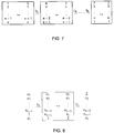
- FIG. 7 is a schematic diagram of a cyclic but not complete n-RMGC arrangement for a flash memory device.
- FIG. 8 is a schematic diagram of a cyclic and complete n-RMGC arrangement for a flash memory device.
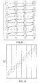
- FIG. 10 is a schematic diagram that shows the charge levels of cells for each programming cycle in a recursive balanced 4-RMGC.
- FIGS. 12A , 12 B, and 12 C are tree diagrams that illustrate cases for computing the opt function in accordance with the invention.
- FIG. 13 is a flow diagram that shows the operations of a data storage device constructed in accordance with the description herein.
- FIG. 14 is a flow diagram that shows reading operations of a data storage device constructed in accordance with the description herein.
- FIG. 15 is a flow diagram that shows programming operations of a data storage device constructed in accordance with the description herein.
- FIG. 16 is an illustration of a memory device constructed in accordance with the present invention.
- FIG. 17 is a block diagram of a computer apparatus to perform the operations of FIGS. 13 , 14 , and 15 and for communicating with a memory device such as depicted in FIG. 16 .
- FIG. 18 is a block diagram that shows data flow in a memory device that operates according to the rank modulation scheme described herein.
- the rank modulation scheme organizes a set of memory cells into a “virtual cell” such that each virtual cell stores information in a permutation determined by the different charge levels of the individual cells in the set. That is, the relative rank of the charge levels in the cells of a single set determines a permutation ordering that represents a codeword.
- the resulting data storage scheme eliminates the need for determining discrete cell charge levels to determine codewords. Therefore, overshoot errors when programming cells (a serious problem that reduces the writing speed of conventional flash memories) are eliminated, and problems with asymmetric errors are mitigated.
- a set of n cells is grouped into a single virtual cell such that each of the n cells has a distinct charge level, and the relative charge level of a cell indicates its rank in the group.
- the set of n cells determines a permutation ⁇ 1, 2, 3, . . . , n ⁇ that corresponds to a codeword.
- the permutation is used to store information.
- the cell with the highest level has the highest (first) rank and is first in the permutation
- the second-highest cell has the next rank, and so forth to define a permutation in order from highest level cell to lowest level cell, such as ⁇ 3, 2, 1 4 ⁇ .
- each permutation can correspond to a different codeword and thereby represent data.
- FIG. 1 is a schematic representation of a memory cell arrangement in accordance with the rank modulation scheme wherein each rectangular box of FIG. 1 represents a conventional multilevel memory cell.
- FIG. 1 shows only four memory cells, for simplicity of illustration, but it should be understood that a typical data storage device, such as a flash memory device, will contain many more cells than illustrated in FIG. 1 .
- A [A 1 , A 2 , A 3 , A 4 ]
- FIG. 1 represents a permutation of [3, 2, 1, 4].
- a flash memory consists of floating-gate cells as its basic storage elements. In most products, a cell has two states and therefore can store one bit, but to increase data density, multi-level storage (where a cell has 4 to 256 or even more states) is either already used or being developed. See P. Cappelletti et al., Chapter 6, “Multilevel Flash Memories”, in Flash Memories , Kluwer Academic Publishers, 1st Edition, 1999. For a cell with q states, we denote them by 0, 1, . . . , q ⁇ 1. These states correspond to the threshold voltages of a cell, and are also called q levels. Different levels correspond to different data values.
- the flash memory uses the hot-electron injection mechanism or the Fowler-Nordheim tunneling mechanism to inject (respectively, remove) charge into (from) the cell.
- the charge can be electrons or holes, depending on if the cells are nFETs or pFETs. The more charge a cell has, the higher its threshold voltage is.
- a flash memory reads data by measuring the cells' threshold voltages.
- a cell with q discrete levels can store at most log 2 q bits. Note that actually, the level of a cell can be changed continuously. However, if the gap between adjacent levels is too small, errors will become common.
- the cells in a flash memory are organized into blocks, where each blocks consists of 64K, 128K or 256K cells. See, for example, P. Cappelletti et al., Chapter 5, “Memory Architecture and Related Issues” in Flash Memories , Kluwer Academic Publishers, 1st Edition, 1999.
- block erasure To decrease a cell's level, the whole block has to be erased, which means lowering all the cells to the lowest level. This is called block erasure. Then the cells are reprogrammed sequentially. Block erasure is a necessary feature of flash memories for circuit compactness.
- Block erasures They significantly slow down the write speed, shorten the memory's lifetime, and waste energy. Each block erasures reduces the cells' quality. After about 10 5 ⁇ 10 6 block erasures, the flash memory will break down. See, for example, S. Aritome et al., Proceedings of the IEEE, 81(5):776-788 (1993); P. Cappelletti et al., supra. Therefore, a better scheme for rewriting (i.e., modifying data) is desirable so that most rewrites will not cause block erasures. Unfortunately, most rewrites as currently performed will cause block erasures. (2) Over-programming.
- Using cell rank order to represent data makes writing and rewriting much simpler, and the cell levels do not have to take discrete values. Instead, they can be continuous. In the above example, the full order of cell levels is used. As a more general (and powerful) scheme, we can use the partial order of cell levels to represent data.
- a rank modulation coding scheme defines a mapping from the (partial) order of a set of cells' levels to data. It also defines a procedure for rewriting data. To change the cell levels from one order to another order, some cells' levels are raised, and they are raised with an important property: when a cell's level is being raised, the only requirement for its targeted level is that the targeted level is higher than some other cell's level. Because of this property, clearly over-programming will never happen in the rank modulation scheme. We will now illustrate rank modulation coding with an example.
- FIGS. 2 , 3 , and 4 illustrate a rank modulation coding scheme that uses three cells to represent a ternary variable.
- the mapping from the order of cell levels to the variable is shown in FIG. 2 .
- the procedure for rewriting is illustrated in FIG. 3 . It is actually relatively simple by examination of the drawings; in a grouping of cells, if a variable's value is changed from i to j, then the j-th cell's level is raised to be the highest level.
- FIGS. 4A , 4 B, and 4 C An example of rewriting is shown in FIGS. 4A , 4 B, and 4 C, where the represented variable changes as from 3 ⁇ 2 ⁇ 1, and the order of the cell levels changes as (3, 2, 1) ⁇ (2, 3, 1) ⁇ (1, 2, 3).
- FIG. 4A represents (3, 2, 1), with cell “3” having the highest charge;
- FIG. 4B represents (2, 3, 1);
- FIG. 4C represents (1, 2, 3).
- rank modulation code features related to this objective are described further below and in the above-referenced co-pending U.S. patent application by Anxiao Jiang, et al. (see the U.S. patent application entitled “Error Correcting Codes for Rank Modulation” by A. Jiang et al. filed Nov. 20, 2008).
- the rank modulation scheme is especially suited for multilevel cell constructions, such as multilevel flash memory devices.
- Error correction techniques for multilevel flash memory devices are quite well-known. Such techniques, however, are not very effective for the errors encountered with different modulation schemes, such as the rank modulation scheme.
- Errors in conventional flash memory devices involve correction of discrete charge level readings from cells. Errors in devices that use a rank modulation data scheme will not involve correction of discrete charge level, but will involve correction of transposition errors in the relative ranking of the cells within a set of cells.
- Rank modulation coding provides a new way to program and store data. We can further improve this scheme by using the joint coding of data to improve load balance, and use error-correcting codes to improve data reliability. In addition, we can intentionally use controlled charge leakage to lower the cell levels uniformly without changing their ranks, thus reducing or even eliminating the need to erase blocks for rewriting data. The details on these topics will be further described below.
- rank modulation coding for memory devices effectively removes the risk of over-programming. It can improve the cell-programming (write) speed, data reliability, and storage capacity.
- This section presents several focused research topics relating to rank modulation coding: cell-programming speed, storage capacity, and data modification capability.
- programming cells In flash memories, programming cells (i.e., writing) is substantially slower than reading cells.
- the writing speed is about 1/10 of the reading speed. See, for example, P. Cappelletti et al., supra. Common read and write speeds are multiple MB per second.
- the slow writing speed is due to the iterative programming process; to avoid over-programming, which can only be corrected by block erasures, the flash memory repeatedly raises the cell's level by small amounts and measures it, until the cell level reaches the targeted value.
- Rank modulation coding can significantly improve the cell programming speed because it removes the risk of over-programming.
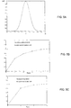
- the following example shows the idea. Consider raising a cell's level from 0 to V. It requires multiple rounds of cell-level increase and measurement. Since flash cells usually have different characteristics, the actual increase is different from the targeted increase. To assist numerical computation, we model the cell-level increase by the truncated Gaussian distribution: when the targeted increase is A, the actual increase has the probability density function
- f ⁇ ( x ) 1 ⁇ ⁇ 2 ⁇ ⁇ ⁇ ⁇ e - ( x - A ) 2 2 ⁇ ⁇ 2 ⁇ 1 p ⁇ ⁇ for ⁇ ⁇ 0 ⁇ x ⁇ 2 ⁇ A , where p is a normalization factor.
- ⁇ 0.2 A. See, for example, the probability density function illustrated in FIGS. 5A , 5 B, and 5 C, given by simulation results. Note that in FIG. 5A , the maximum increase is 2 A, twice the expected value, which is observable in flash memory experiments.
- FIG. 5B shows how the cell level approaches the final level.
- Rank modulation coding removes the risk of over-programming.
- the objective is that the final cell level should be at least V(1 ⁇ ) and on average be V. Since there is no constraint on how large the cell level can be in the worst case, the expected increase in each round can be set larger.
- a numerical simulation shows that on average, 2.63 rounds of increase-measurement are needed for programming a cell. See FIG. 5C . This means that rank modulation coding can improve the cell-programming speed by 93%.
- Rank modulation coding can help improve the storage capacity due to its tolerance of asymmetric errors.
- a major source of errors is charge leakage, which means that cells gradually lose charge, and their levels decrease consequently.
- Rank modulation coding uses the ranks of cell levels to represent data, and such asymmetric errors affect the ranks less significantly than affecting their absolute values.
- Rank modulation coding provides a new paradigm for studying the fundamental tradeoff between the storage capacity, the writing speed, and the rewriting capability of flash memories.
- the storage capacity can be optimized based on the speed, reliability, and circuit complexity of flash memories.
- Such an approach generally has two shortcomings: (1) before the old block is reused, the storage capacity is under-used, because the old block is being wasted; (2) even if only a small portion of the data are actually modified, still the whole block is rewritten, which makes the rewriting slow. That gives us motivations to study rewriting data locally in the same block until the cell levels reach the maximum level. The objective is to maximize the number of rewrites before a block erasure becomes necessary.
- the coding schemes studied in this project can increase the number of rewrites by O(log l) times compared to current flash file systems. With joint coding, which will be presented in the next section, the performance gain can be even much bigger.
- rank modulation code based on partial order has been described, where two ternary variables are jointly stored.
- the code can be easily extended to store a single variable.
- the basic reason is that when partial orders are used, the gap between two cell levels that are not compared can be arbitrary (including being arbitrarily small).
- the technology may allow in the near future the decrease of all the charge levels in a block of cells by a substantially uniform (constant) amount smaller than the lowest charge level (block deflation), which would maintain their relative values, and thus leave the information unchanged. This can eliminate a designated erase step, by deflating the entire block whenever the memory is not in use.
- Gray codes that bring to bear the full representational power of rank modulation, and data rewriting schemes.
- the Gray code is an ordered list of distinct length n binary vectors such that every two adjacent words (in the list) differ by exactly one bit flip. See, for example, Gray, F. “Pulse Code Communication,” U.S. Pat. No. 2,632,058 (March 1953).
- T is the set of all possible single bit flips.
- the set T consists of transitions that are minimal with respect to some cost function, thus creating a traversal of the state space that is minimal in total cost.
- Gray codes One application of the Gray codes is the realization of logic multi-level cells with rank modulation.
- the traversal of states by the Gray code is mapped to the increase of the cell level in a classic multi-level flash cell. In this way, rank modulation can be naturally combined with current multi-level storage solutions.
- Some of the Gray code constructions we describe also induce a simple algorithm for generating the list of permutations. Efficient generation of permutations has been the subject of much research as described in the general survey (Savage, C. D. SIAM Rev., 39(4):605-629, (December 1997)), and the more specific (Sedgewick, R. Computing Surveys, 9(2):137-164, (June 1977)) (and references therein). In (Sedgewick, R. Computing Surveys, 9(2):137-164, (June 1977)), the transitions we use in this paper are called “nested cycling,” and the algorithms cited there produce lists that are not Gray codes since some of the permutations repeat, which makes the algorithms inefficient.
- Rank modulation is a new storage scheme and differs from existing data storage techniques.
- flash memories There has been some recent work on coding for flash memories. Examples include floating codes (Jiang, A. Proceedings of the 2008 IEEE International Symposium on Information Theory ( ISIT 2008), Toronto, Cariada, pp. 1741-1745 (July 2008); (Jiang, A. et al., Proceedings of the 2007 IEEE International Symposium on Information Theory ( ISIT 2007), Nice, France, pp. 1166-1170 (June 2007)), which jointly record and rewrite multiple variables, and buffer codes (Bohossian, V. et al., IEEE International Symposium on Information Theory ( ISIT 2007), Nice, France, pp. 1186-1190 (June 2007); Yaakobi, E.
- Floating codes are an extension of the write-once memory (WOM) codes (see, e.g., Cohen, G. D. et al., IEEE Trans. on Inform. Theory , IT-32(5):697-700, (September 1986); Fiat, A. et al., IEEE Trans. on Inform. Theory , IT-30(3):470-480, (May 1984); Fu, F.-W.
- WOM write-once memory
- Section II describes a Gray code that is cyclic and complete (i.e., it spans the entire symmetric group of permutations);
- Section III introduces a Gray code that is cyclic, complete and balanced, optimizing the transition step and also making it suitable for block deflation;
- Section IV shows a rewriting scheme that is optimal for the worst-case rewrite cost;
- Section V presents a code optimized for the average rewrite cost with small approximation ratios;
- Section VI concludes this paper.
- [n] denote the set of integers ⁇ 1, 2, . . . , n ⁇ .
- the state space for the rank modulation scheme is therefore the set of all permutations over [n], denoted by S n .
- the basic minimal-cost operation on a given state is a “push-to-the-top” operation by which a single cell has its charge level increased so as to be the highest of the set.
- Example 1 An Example of a 3-RMGC is given by the following Table 1:
- Gray codes One important application of the Gray codes is the realization of logic multi-level cells.
- the traversal of states by the Gray code is mapped to the increase of the cell level in a classic multi-level flash cell.
- n-RMGC As an n-RMGC has n! states, it can simulate a cell of up to n! discrete levels.
- Current data storage schemes can therefore use the Gray codes as logic cells, as illustrated in FIG. 6 , and get the benefits of rank modulation. See, for example, floating codes as described in Jiang, A. et al., Proceedings of the 2007 IEEE International Symposium on Information Theory ( ISIT 2007), Nice, France, pp. 1166-1170 (June 2007).
- FIG. 6 shows how RMGCs can be used to realize logic q-level cells, which are useful for conventional data storage schemes that store data such as floating codes.
- the upper portion of FIG. 6 shows a conventional data storage scheme to store logic q-level cells, whereas the lower portion of FIG. 6 shows a corresponding RMGC coding scheme that can store the same information.
- the second element in the first permutation in every block is “2”.
- the first element in the last permutation in every block is also “2”.
- Lemma 3 In any block, the last element of all the permutations is constant. The sequence of last elements in the blocks constructed is (n, n ⁇ 1, . . . , 3, 1). The element “2” is never a last element.
- the first claim is easily proved by noting that the transitions creating a block, t i1 , t i2 , . . . , t i(n ⁇ 1)! ⁇ 1 , only operate on the first n ⁇ 1 positions of the permutations. Also, by the same logic used in the proof of the previous lemma, if the first permutation of a block is [a 1 , a 2 , a 3 , . . . a n ⁇ 1 , a n ], then the last permutation in a block is [a 2 , a 1 , a 3 , . . .
- the first permutation of the next block is [a 1 , a 2 , a 1 , a 3 , . . . , a n ⁇ 1 ].
- each box represents a single block, and the curved arrow ( ) denotes the sequence of transitions (t i1 , . . . , t i(n ⁇ 1)! ⁇ 1 ).
- C′ we look for a transition of the following form: [a 2 , . . . , a n ⁇ 1 , 2, a 1 ] ⁇ [2, a 2 , . . . , a n ⁇ 1 , a 1 ].
- C′ does not contain permutations in which “2” is last, while it does contain permutations in which “2” is next to last, and some where “2” is the first element. Since C′ is cyclic, there must be at least one transition t n ⁇ 1 pushing an element “2” from a next-to-last position to the first position.
- C′ is cyclic, there must be at least one transition t n ⁇ 1 pushing an element “2” from a next-to-last position to the first position.
- the jump in the p-th round is defined as c i (p)-c i (p ⁇ 1), assuming the i-th cell was the affected one. It is desirable, when programming cells, to make the jumps as small as possible.
- n ⁇ 3 we must raise the lowest cell to the top charge level at least n times. Such a jump must be at least of magnitude n. We cannot, however, do these n jumps consecutively, or else we return to the first permutation after just n steps. It follows that there must be at least one other transition t i , i ⁇ n, and so the first t n to be used after it jumps by at least a magnitude of n+1.
- n-RMGC with a jump cost of n+1 a balanced n-RMGC.
- the intuitive idea is to base the construction on cyclic shifts t n that push the bottom to the top, and use them as often as possible. This is desirable because t n does not introduce gaps between the charge levels, so it does not aggravate the jump cost of the cycle.
- Theorem 6 gives a construction where these orbits are traversed consecutively, based on the order given by the supporting (n ⁇ 1)-RMGC.
- t j k ⁇ t n - i ⁇ k / n ⁇ + 1 , k ⁇ 1 ⁇ ( mod ⁇ ⁇ n ) t n , otherwise ⁇ ⁇ for ⁇ ⁇ all ⁇ ⁇ k ⁇ ⁇ 1 , ... ⁇ , n ! ⁇ .
- t i ⁇ ⁇ ( ⁇ ) ( t n ⁇ ... ⁇ t n ⁇ ⁇ n - 1 ⁇ ⁇ times ⁇ t n - i + 1 ) ⁇ ( ⁇ ) , ⁇ ⁇ ⁇ S n .
- the code C n is balanced, because in every block of n transitions starting with a t n ⁇ i+1 , 2 ⁇ i ⁇ n ⁇ 1, we have: the transition t n ⁇ i+1 has a jump of n ⁇ i+1; the following i ⁇ 1 transitions t n have a jump of n+1, and the rest a jump of n.
- C n ⁇ 1 is cyclic and complete, it follows that C n is also cyclic and complete.
- the permutations are represented in an n ⁇ (n ⁇ 1)! matrix, where each row is an orbit generated by t n .
- These transitions are defined recursively by a balanced 3-RMGC over the set ⁇ 1, 2, 3 ⁇ , which is identical to the one from Example 1. Notice that the supporting 3-RMGC is reflected (e.g., written upside down) in the permutations of [4] that are exit points from the orbits.
- the balanced n-RMGC can be used to implement a logic cell with n! levels. This can also be understood as a counter that increments its value by one unit at a time.
- Successor (n, [a 1 , . . . , a n ]) is depicted below in pseudocode to describe the sequence of operations performed in a memory device constructed in accordance with this description.
- a step is defined as a single query of the form “what is the i-th highest charged cell?”, namely the comparison in line 4.
- the Successor function is asymptotically optimal with respect to this measure:
- Theorem 10 In the Successor function, the asymptotic average number of steps to create the successor of a given permutation is 1.
- n - 2 n - 1 of the transitions are determined by just one more step, and so on.
- permutations over two elements require zero steps. Equivalently, the query “is a 1 equal to n” is performed for every permutation, therefore n! times; the query “is a n equal to n ⁇ 1” is performed only for
- the digit do is always 0, and is sometimes omitted:
- Any permutation [a 1 , . . . , a n ] has a unique factoradic representation that gives its position in the lexicographic ordering.
- the digits d i are in this case the number of elements smaller than a n ⁇ i that are to the right of a n ⁇ i . They are therefore inversion counts, and the factoradic representation is an inversion table (or vector). See, for example, Hall, M. Jr. et al., Amer. Math. Monthly, 72(2):21-28, (1965).
- B-Factoradic A New Numbering System.
- index permutations of the balanced recursive n-RMGC with numbers from ⁇ 0, . . . , n! ⁇ 1 ⁇ such that consecutive permutations in the cycle have consecutive ranks modulo n!.
- the permutation that gets index 0 is a special permutation that starts a new orbit generated by t n , and also starts new orbit in any of the recursive supporting n′-RMGCs, n′ ⁇ n ⁇ 1, . . . , 2 ⁇ .
- the rank of a permutation is determined by its position in the orbit of t n , and by the rank of the orbit, as given by the rank of the supporting permutation of [n ⁇ 1].
- Equation (1) induces a new numbering system that we call b-factoradic (backwards factoradic).
- a number m ⁇ 0, . . . , n! ⁇ 1 ⁇ can be represented by the digits b n ⁇ 1 b n ⁇ 2 . . . b 1 b 0 , where b i ⁇ 0, . . . , n ⁇ 1 ⁇ i ⁇ and the weight of b i is n!/(n ⁇ i)!.
- b n ⁇ 1 is always 0 and can be omitted. It is easy to verify that this is a valid numbering system, therefore any m ⁇ 0, . . . , n! ⁇ 1 ⁇ has a unique b-factoradic representation such that:
- weights of the b-factoradic are sometimes called “falling factorials”, and can be represented succinctly by the Pochhammer symbol.
- Example 11 can be formalized algorithmically, however its time complexity is O(n 2 ), similar to the naive algorithms specific to translations between permutations in lexicographic order and factoradic.
- We can thus leverage directly all the results available for factoradic, and use them to determine the current symbol of a logic cell.
- a b-factoradic digit b k is a count of the elements smaller than n ⁇ k that lie between n ⁇ k+1 and n ⁇ k when the permutation is viewed as a cycle. The direction of the count alternates for even and odd values of k.
- the inverse of the input permutation v can be computed in O(n) time (line 1 of the pseudocode). The position of every element of the permutation can then be computed in constant time (lines 2 and 5).
- the test in line 6 decides if we count towards the right or left starting from the position i that holds element n ⁇ k+1, until we reach position j that holds element n ⁇ k.
- i ⁇ j and j ⁇ i we obtain the formulas in lines 7 and 9. Since this computation takes a constant number of arithmetic operations, the entire algorithm takes O(n) time.
- Unranking namely going from a number in ⁇ 0, . . . , n! ⁇ 1 ⁇ to a permutation in balanced order
- the logic cell is designed to be a counter.
- Unrank takes a b-factoradic as input and produces the corresponding permutation.
- the procedure uses variable p to simulate the cyclic counting of elements smaller than the current one. The direction of the counting alternates, based on the test in line 4 of the pseudocode.
- the permutation induced by the charge levels of the cells represents the information through the interpretation function.
- the permutation is changed using the “push-to-the-top” operations based on the update function.
- the number of “push-to-the-top” operations determines not only the rewriting delay but also how much closer the highest cell-charge level is to the system limit (and therefore how much closer the cell block is to the next costly erase operation).
- the objective of the coding scheme is to minimize the number of “push-to-the-top” operations.
- the worst-case rewrite cost is defined as:
- V the transition graph
- S n the transition graph
- G is a regular digraph, because every vertex has n ⁇ 1 incoming edges and n ⁇ 1 outgoing edges.
- v ⁇ B r n (u) It follows that v can be obtained from u with at most r “push-to-the-top” operations. Those elements pushed to the top appear in the first r positions of v, so the last n ⁇ r positions of v contain elements which have the same relative order in u, thus, v ⁇ P u .
- Lemma 16 Fix integers n and l, and define ⁇ (n, l) to be the smallest integer such that
- W n and any state s ⁇ W n there exists i ⁇ [l] such that ⁇ (s ⁇ (s, i)) ⁇ (n, l), i.e., the worst-case rewrite cost of any code is at least ⁇ (n, l).
- a prefix sequence a [a (1) , a (2) , . . . , a (m) ] is a sequence of m ⁇ n distinct symbols from [n].
- the prefix set P n (a) ⁇ S n is defined as all the permutations in S n which start with the sequence a.
- Theorem 19 The code in Construction 18 is optimal in terms of minimizing the worst-case rewrite cost.
- n ! ( n - m ) ! ⁇ B m n ⁇ .
- the number of prefix sequences of length ⁇ (n, l) is at least l, which allows the first of the construction.
- the worst-case rewrite cost of the construction is at most ⁇ (n, l).
- the prefix sequences are no longer necessarily of the same length. We do, however, require that no prefix sequence be the prefix of another.
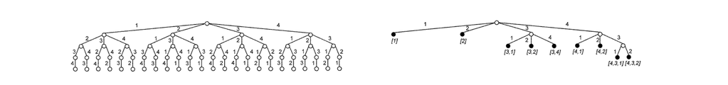
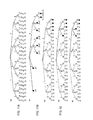
- FIG. 11A and FIG. 11B depict tree diagrams for permutations useful in rank modulation codes.
- a full permutation tree T as follows.
- the edges are labeled in such a way that every leaf corresponds to a permutation from S n which may be constructed from the labels on the edges from the root to the leaf. This example corresponds to the tree given in FIG.
- a prefix-free code corresponds to a subtree C of T.
- An example of a subtree prefix-free code is given by FIG. 11B , the lower tree of the illustration. Every leaf is mapped to a prefix sequence which equals the string of labels as read on the path from the root to the leaf.
- the prefix sequence representing i For example, the prefix sequences in FIG. 4( b ) have minimum length 1 and maximum length 3.
- the average codeword length is defined as
- ⁇ i 1 l ⁇ p i ⁇ ⁇ a i ⁇ .
- the probabilities p i are as defined before, that is, information symbols are i.i.d. random variables having value i ⁇ [l] with probability p i .
- Our objective is to design a prefix-free code that minimizes its average codeword length.
- the optimal prefix-free code cannot be constructed with a greedy algorithm like the Huffman code, because the internal nodes in different layers of the full permutation tree T have different degrees, making the distribution of the vertex degrees in the code tree C initially unknown.
- the Huffman code is a well-known variable-length prefix-free code, and many variations of it have been studied. See, for example, Huffman, D. A. Proceedings of the Institute of Radio Engineers, 40(9):1098-1101, (1952). In Hwang, F. K. SIAMJ. Appl. Math., 37(1):124-127, (1979), the Huffman code construction was generalized, assuming that the vertex-degree distribution in the code tree is given. In Baer, M. B. IEEE Trans. on Inform.
- opt i (x, m) we interpret the meaning of opt i (x, m) as follows.
- the subtree has exactly x leaves in the layers i, i+1, . . . , n ⁇ 1. It also has at most m vertices in the layer i.
- the x leaves represent the x letters from the alphabet [l] with the lowest probabilities p j : the further the leaf is from the root, the lower the corresponding probability.
- Those leaves also form x prefix sequences, and we call their weighted average length (where the probabilities p j are weights) the value of the subtree.
- the minimum value of such a subtree is defined to be opt i (x, m).
- opt i (x, m) is the minimum average prefix-sequence length when we assign a subset of prefix sequences to a subtree of T (in the way described above).
- the minimum average codeword length of a prefix-free code equals opt 1 (l, n).
- the algorithm first computes opt n ⁇ 1 (x, m), then opt n ⁇ 2 (x, m), and so on, until it finally computes opt 1 (l, n), by using the above recursions. Given these values, it is straightforward to determine in the optimal code, how many prefix sequences are in each layer, and therefore determine the optimal code itself. It is easy to see that the algorithm returns an optimal code in time O(nl 4 ).
- opt 2 (4, 3) corresponds to a subtree of T with a total of four leaves in layer 2 and layer 3 , and with at most three vertices in layer 2 .
- the corresponding subtrees in the first three cases are as shown in the tree diagrams of FIGS. 12A , 12 B, 12 C, respectively.
- the fourth case is actually impossible, because it leaves no place for the fourth leaf to exist in the subtree.
- the solid-line edges are the remaining edges in the full-permutation tree T.
- the leaves in the respective subtrees are shown as black vertices.
- FIG. 12A there are no leaves in layer 2 .
- FIG. 12B there is one leaf in layer 1 .
- FIG. 12C there are two leaves in layer 2 .
- layer 2 has i leaves (0 ⁇ i ⁇ 3), then layer 3 has 4 ⁇ i leaves and there can be at most (3 ⁇ i) ⁇ 2 vertices in layer 3 of the subtree.
- p 1 , p 2 , p 3 , p 4 to the four leaves and minimize the weighted average distance of the leaves to the root (which is defined as opt 2 (4, 3)), among the four cases mentioned above, we choose the case that minimizes that weighted average distance. Therefore,
- s′ l ⁇ 1 ⁇ S n ⁇ s i ⁇ the l ⁇ 1 closest permutations to s i ordered by increasing distance, i.e., ⁇ ( s i ⁇ s′ 1 ) ⁇ ( s i ⁇ s′ 2 ) ⁇ . . . ⁇ ( s i ⁇ s′ l ⁇ 1 ), and denote ⁇ j a (s i ⁇ s′ j ) for every j ⁇ [l ⁇ 1].
- the average rewrite cost of a stored symbol i ⁇ [l] using a code X is the weighted sum
- ⁇ C ⁇ ( i ) ⁇ j ⁇ [ l ] , j ⁇ i ⁇ p j ⁇ ⁇ ⁇ ( s i ⁇ ⁇ C ⁇ ( s i , j ) ) .
- Z(i) is not necessarily a prefix-free code with minimal average codeword length.
- A be a prefix-free code that minimizes its average codeword length.
- ⁇ A (s) the average rewrite cost of a rewrite operation under A starting from state s.
- ⁇ m 1 n - 1 ⁇ r m ⁇ ⁇ ( n - m ) ! n ! ⁇ 1.
- the prefix sequence z j (i) represents the information symbol j, which is associated with the probability p j in rewriting.
- Theorem 26 Fix some l ⁇ n!/2 and let A be a prefix-free code over [l] which minimizes its average codeword length. For any rewrite operation with initial stored information symbol i ⁇ [l], ⁇ A ( i ) ⁇ 3 ⁇ ( i ), i.e., the average cost of rewriting i under A is at most three times the lower bound.
- p i ′ ⁇ p i ⁇ ⁇ i ⁇ [ l ] 0 ⁇ ⁇ i ⁇ [ l ′ ] ⁇ ⁇ [ ⁇ l ] .
- A′ be a prefix-free code over [l′] which minimizes its average codeword length.
- ⁇ (i) the lower bound on the average rewrite cost of symbol i, does depend on the probability distribution of the input symbols. Let us therefore distinguish between ⁇ (i) over [l], and ⁇ ′(i) over [l′]. However, by definition, and by our choice of probability distribution over [l],
- Theorem 28 Fix some l ⁇ n!/6, n ⁇ 4, and let A be a prefix-free code over [l] which minimizes its average codeword length. For any rewrite operation with initial stored information symbol i ⁇ [l], ⁇ A ( i ) ⁇ 2 ⁇ ( i ), i.e., the average cost of rewriting i under A is at most twice the lower bound.
- n/2 cells are used to store each variable.
- the rank modulation code in Example 1 can be used. That is, partition the n/2 cells into groups of three, and use them sequentially to store the variable. Its performance can be measured as follows. Since the code in Example 1 uses the full order of cells to represent data, let A denote the margin between two adjacent cell levels. For simplicity, assume A to be a constant. Let V max denote the maximum level for cells. Then, when the variable is initially written, the cell levels are 0, ⁇ , and 2 ⁇ . Each rewriting of the variable raises a cell's level to the top, so a group of three cells support
- V max ⁇ - 1 writes.
- the n/2 cells totally support
- n cells as if they are in an array with a rows and b columns: call the cells c i,j , where 1 ⁇ i ⁇ a, 1 ⁇ j ⁇ b.
- the b cells are divided into three types based on their functions: c i,1 , c i,2 , c i,3 are index cells, c i,4 is the reference cell, and the other b ⁇ 4 cells—c i,5 , . . .
- V 1 ⁇ i ⁇ S 1 ⁇ C i + ⁇ i ⁇ S 2 ⁇ 2 ⁇ C i (mod 3), and
- V 2 ⁇ i ⁇ S 3 ⁇ C i + ⁇ i ⁇ S 4 ⁇ 2 ⁇ C i ⁇ ( mod ⁇ ⁇ 3 ) .
- Those type-5 rows represent neither variable.
- the above joint coding approach can be generalized to jointly store k l-ary variables, for any k ⁇ 1 and l ⁇ 2. Compared to separate coding, the increase in the rewriting performance can be nearly
- joint coding which generalizes the rank permutation coding—is a potentially very powerful tool to balance cell loads.
- the above code for load balancing can be generalized to a code that uses the partial order of n cells' levels to jointly store k l-ary variables. Compared to separate storage of the k variables, this code can rewrite the variables nearly
- Load balancing is a bottleneck hindering the improvement of flash memories.
- By jointly storing multiple variables no matter how uneven the variables' modification frequencies are, the number of allowed rewrites can still be large. This way, we can significantly improve the average write speed and power efficiency.
- Such a coding scheme is especially suitable for NOR flash memories, which have random access to cells. It is fundamentally different from the wear-leveling techniques used in current flash file systems, which are techniques for balancing the usage of the blocks (not the cells in a block), so that the blocks wear out evenly. Wear-leveling does not really reduce block erasures. Joint coding, on the contrary, aims at reducing block erasures as much as possible. See, for example, P. Cappelletti et al. supra, E. Gal et al., supra, and Saifun Semiconductors Ltd. Web site, available at the Internet URL of www.saifun.com.
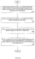
- FIG. 13 is a flow diagram that shows the operations of a data storage device using the rank modulation coding scheme as described herein.
- the data storage device may comprise a variety of systems and components, whether as a device external to computing devices for data storage, or integrated with other components of a system for data storage.
- the data storage device may be implemented, for example, as a Flash memory external device, such as a USB-compatible “thumb drive” or the like, or the storage device may be implemented as an internal component such as a “solid state drive” (SSD) for use in place of a hard disk drive in desktop and laptop computers.
- SSD solid state drive
- the data storage device receives data for programming (storage) from a host device, and provides data read from the data storage to a host device.
- the host device may comprise the computing device with which the thumb drive communicates via the USB data channel, and in the case of the SSD, the host device may comprise the SSD controller that manages the data interface to an associated system bus of a computer in which the SSD is installed.
- a data storage device that operates in accordance with the rank modulation scheme determines a permutation of a codeword that corresponds to a data value. That is, such a device represents permutations as cells such that a group of cells represent a single virtual cell associated with a permutation corresponding to data.
- This is illustrated by the flow chart box 1302 of FIG. 13 , which shows that the device receives a data value to be encoded into a codeword, wherein the codeword indicates n cell values that comprise a virtual cell in which relative rank ordering of the n cell values determines a permutation comprising one of n! permutations.
- the device Having generated the permutation, the device then provides the permutation to a data destination over an information channel.
- the data destination may comprise memory cells, such as flash memory, or the data destination may comprise a transmitter, in the case where the cells comprise signal features, as explained further in the next paragraph.
- storage elements may be associated with respective levels of stored charge, and the a i values of the permutation A may be stored in the storage elements by setting the stored charge levels in the storage elements of the virtual cell such that the highest charge level corresponds to the a 1 storage element and the lowest charge level corresponds to the a n storage element.
- the virtual cell may be represented by a signal and the cell values comprise signal features, such as signal frequency, magnitude, or duration.
- the device may receive or transmit a signal in which the signal frequency, magnitude, or duration is modified over time so as to define cells or bins, wherein the portion of the signal having the greatest frequency, magnitude, or duration is denoted the highest level cell in a corresponding permutation, and the next highest signal portion is the next highest cell, and so forth.
- the next flowchart box 1304 indicates that the data storage device can be operated so as to perform a read sequence of operations to receive a permutation that corresponds to a codeword and determine a corresponding data value.
- the read sequence 1304 operations may include comparing the stored charge levels of the storage elements, identifying the storage element with the greatest stored charge level, and determining a set of values that corresponds to the permutation A stored in the virtual cell. Reading data by simply determining rank ordering of storage element charge levels for determining a permutation that corresponds to data values is potentially much faster than determining exact voltage levels of storage elements to determine corresponding data values.
- Box 1306 shows that the storage device can also be operated so as to perform a program sequence of operations to receive data from a host device and program (write or store) the data into the device.
- Box 1306 represents a program sequence that includes increasing the stored charged level of one storage element in the virtual cell from a current charge level to an increased charge level, such that the increased charge level is greater than the stored charge level of any other storage element.
- Storing data by increasing the stored charge level of one storage element to the highest charge level of any storage element within a virtual cell a “push-to-top” operation, is potentially much faster than changing the charge level to be an exact voltage level, which may involve initially performing a block erasure operation.
- the “push-to-top” operation also greatly reduces the risk of overshooting the desired exact voltage level, which requires a block erasure operation.
- rank modulation coding vastly reduces the need for block erasure during write operations.
- the operations of programming a value into the data storage device may include joint coding operations such that multiple storage elements are used to represent multiple data items (also called variables) in a joint way (namely, the storage elements are not necessarily separated into groups with each group representing one variable separately).
- the multiple data items may be rewritten with different frequencies.
- the permutations of the storage elements are mapped to the multiple data items.
- the permutations of the storage elements can be partial ordering, which is a special case of permutation where some storage elements are not compared and so the relative orders between them do not matter.
- the coding of the plurality of storage elements may include storage elements designated as index cells, reference cell, or cells representing integers such that the stored data items are some linear combinations of those integers. It should be apparent that any joint coding operations that were performed upon programming data values into the data storage device will likewise be performed upon reading from the data storage device.
- Box 1308 shows an optional uniform stored charge reduction operation that is unique to rank modulation code storage devices that have memory cells.
- the uniform stored charge reduction operation can further reduce block erasure operations, and comprises decreasing the stored charge level in all the storage elements in a virtual cell by a constant charge amount that is less than the lowest stored charge level of the storage elements. This operation can be performed during idle times or as background processing. Uniformly reducing the stored charge levels of all storage elements within a virtual cell will not change the relative rank ordering and therefore will not change the stored value of the virtual cell.
- Uniform charge reduction can be carried out by a controller of the storage device. This can essentially eliminate the need for block erasure operations in a rank modulation code device.
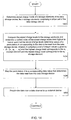
- FIG. 14 is a flow diagram that shows reading operations of a data storage device that includes storage elements such as memory cells.
- the permutation then determines a corresponding data value.
- the data storage device determines the stored charge levels of the n storage elements comprising a virtual cell of the data storage device.
- the techniques used for determining stored charge levels in devices may be conventional techniques, which should be understood without further explanation.
- the data storage device compares the stored charge levels in the storage elements and determines a ranked order of the stored charge levels from highest to lowest such that the stored charge levels determine values of the permutation A corresponding to the data to be read from the data storage device.
- the storage device maps the permutation A to a corresponding data value that determines the data read from the data storage device.
- n-RMGC length-n Rank Modulation Gray Code
- the n-RMGC can be generated in such a way that it is a cyclic and complete code, or it may be generated so that it is cyclic, complete, and balanced.
- the read operations may comprise inverse operations to the code generation. That is, if a particular methodology is used to generate a permutation A given a received data value x for storage, then a reverse set of operations may be carried out to generate a data value x given a permutation A. Such inverse operations will be apparent to those skilled in the art in view of the description herein.
- the storage device provides the data value over a data channel to a host device.
- the rank modulation code may be implemented for an information channel comprising a transmitted signal, rather than comprising a data connection to memory cells.
- the read operation corresponds to receiving a signal and determining signal features, rather than reading memory cell charge levels.
- the signal features can comprise modulation of the signal frequency, magnitude, or duration over time.
- the comparing operation (box 1404 ) relates to determining a rank ordering of the signal features.
- the highest detected signal frequency over a predetermined duration defines the highest cell value
- the next highest detected signal frequency defines the next highest cell value, and so forth, to determine a permutation comprising a codeword.
- the determined permutation is mapped to a data value.
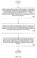
- FIG. 15 is a flow diagram that shows programming operations of a data storage device that includes storage elements such as memory cells.
- Box 1504 indicates that the next program operation is to determine the a i values of the permutation A for storing the a i values into a plurality of storage elements of the data storage device, wherein relative rank ordering of the stored values of the storage elements in the virtual cell corresponds to the permutation A and wherein the storage elements are associated with respective levels of stored charge.
- the permutation can be determined in accordance with rank modulation codes as described previously, which may include cyclic and complete codes, and balanced, cyclic, and complete codes, using the techniques described previously.
- the rank modulation code may comprise an n-RMGC type of code for n storage elements within a virtual cell.
- the permutation to be stored can be determined in accordance with a joint coding scheme such that multiple storage elements are used to represent multiple data items (also called variables) in a joint way.
- the data items can be rewritten at different rewrite rates (rewrite frequencies), and the permutations can be coded according to partial ordering.
- the permutation may be determined so as to include a plurality of storage elements designated as index cells, reference cell, or cells representing integers such that the stored data items are some linear combinations of those integers.
- Box 1506 indicates that the next program operation comprises storing the a i values of the permutation A in the storage elements.
- This operation is performed by setting the stored charge levels in the storage elements of the virtual cell such that the highest charge level corresponds to the a 1 storage element and the lowest charge level corresponds to the a n storage element.
- the program operation stores the permutation A in the storage elements of the virtual cell by raising the charge level of the i-th storage element of the virtual cell, for 2 ⁇ i ⁇ n, above the current highest ranking charge level according to a transition function t i given by t i ( a 1 , . . . , a i ⁇ 1 , a i , a i+1 , . . .
- n n a lengthen Rank Modulation Gray Code (n-RMGC) having n! states.
- n-RMGC lengthen Rank Modulation Gray Code
- raising the charge level of the i-th storage element comprises increasing the stored charge level by a predetermined incremental amount.
- the precision needed for the incremental amount is greatly reduced over conventional data storage techniques for multi-level cells, because the incremental amount need only be sufficient to distinguish relative ranking of the stored charge level of the storage elements within a virtual cell.
- the rank modulation code may be implemented for an information channel comprising a transmitted signal, rather than comprising a data connection to memory cells.
- the data value receiving operation (box 1502 ) would still comprise receiving a data value for encoding, except that the data values would comprise signal modulations for transmission over a communications channel, rather than storing in memory cells.
- determining the values of a permutation (box 1504 ) would still be performed, albeit for purposes of signal modulation rather than setting charge level.
- the operation of setting charge level (box 1506 ) would instead comprise transmitting a signal that is modulated according to the predetermined signal feature to be manipulated (e.g., signal frequency, magnitude, or duration). The details of such operations will be known to those skilled in the art.
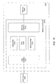
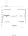
- FIG. 16 is an illustration of a data device constructed in accordance with the present invention.
- FIG. 16 shows a memory 1602 that is accessed by a memory controller 1604 that communicates with a host device 1606 .
- the memory 1602 is used for storing data that is represented in accordance with a rank modulation coding scheme.
- the memory may be implemented, for example, as a Flash memory having multilevel cells.
- the memory 1602 and memory controller 1604 together comprise a data storage device 1608 that may be external to the host device or may be integrated with the host device into a single component or system.
- the data storage device 1608 may comprise a Flash memory device (often referred to as a “thumb drive”) that communicates with a host computer 1606 via a USB connection, or the data storage device may comprise a solid state drive (SSD) that stores data for a host computer system.
- the data storage device may be integrated with a suitable host device to comprise a single system or component with rank modulation memory, such as a smart phone, network router, MP3 player, or the like.
- the memory controller 1604 operates under control of a microcontroller 1610 , which manages communications with the memory 1602 via a memory interface 1612 and manages communications with the host device via a host interface 1614 .
- the memory controller supervises data transfers from the host 1606 to the memory 1602 and from the memory 1602 to the host 1606 .
- the memory controller 1604 also includes a data buffer 1616 in which data values may be temporarily stored for transmission over the data channel controller 1617 between the memory 1602 and the host 1606 .
- the memory controller also includes an ECC block 1618 in which data for the ECC is maintained.
- the ECC block 1618 may comprise data and program code to perform error correction operations for rank modulation code. Such error correction operations are described, for example, in the U.S.
- the ECC block 1618 may contain parameters for the error correction code to be used for the memory 1602 , such as programmed operations for translating between received symbols and error-corrected symbols, or the ECC block may contain lookup tables for codewords or other data, or the like.
- the memory controller 1604 performs the operations described above for decoding data and for encoding data.
- the operations described above for operating a data storage device, for reading data from a device, for programming a data storage device, and encoding and decoding, can be carried out by the operations depicted in FIGS. 13 , 14 , and 15 , which can be performed by the microcontroller 1610 and associated components of the data storage device 1608 .
- the operations depicted in FIGS. 13 , 14 , and 15 can be carried out by the microcontroller 1610 and associated components of the data storage device 1608 .
- the microcontroller 1610 and associated components of the data storage device 1608 For example, in an implementation of the rank modulation coding scheme in a USB thumb drive, all the components of the data storage device 1608 depicted in FIG. 16 are contained within the USB thumb drive.
- the processing components such as the controller 1604 and microcontroller 1610 may be implemented in the form of control logic in software or hardware or a combination of both, and may comprise processors that execute software program instructions from program memory, or as firmware, or the like.
- the host device 1606 may comprise a conventional computer apparatus.
- a conventional computer apparatus also may carry out the operations of FIGS. 13 , 14 , and 15 .
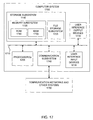
- FIG. 17 is a block diagram of a computer apparatus 1700 sufficient to perform as a host device and sufficient to perform the operations of FIGS. 13 , 14 , and 15 .
- FIG. 17 is a block diagram of a computer system 1700 that may incorporate embodiments of the present invention and perform the operations described herein.
- the computer system 1700 typically includes one or more processors 1705 , a system bus 1710 , storage subsystem 1715 that includes a memory subsystem 1720 and a file storage subsystem 1725 , user interface output devices 1730 , user interface input devices 1735 , a communications subsystem 1740 , and the like.
- the computer system 1700 typically includes conventional computer components such as the one or more processors 1705 .
- the file storage subsystem 1725 can include a variety of memory storage devices, such as a read only memory (ROM) 1745 and random access memory (RAM) 1750 in the memory subsystem 1720 , and direct access storage devices such as disk drives.
- the direct access storage device may comprise a rank modulation data storage device that operates as described herein.
- the user interface output devices 1730 can comprise a variety of devices including flat panel displays, touchscreens, indicator lights, audio devices, force feedback devices, and the like.
- the user interface input devices 1735 can comprise a variety of devices including a computer mouse, trackball, trackpad, joystick, wireless remote, drawing tablet, voice command system, eye tracking system, and the like.
- the user interface input devices 1735 typically allow a user to select objects, icons, text and the like that appear on the user interface output devices 1730 via a command such as a click of a button or the like.
- Embodiments of the communication subsystem 1740 typically include an Ethernet card, a modem (telephone, satellite, cable, ISDN), (asynchronous) digital subscriber line (DSL) unit, FireWire (IEEE 1394) interface, USB interface, and the like.
- the communications subsystem 1740 may be coupled to communications networks and other external systems 1755 (e.g., a network such as a LAN or the Internet), to a FireWire bus, or the like.
- the communications subsystem 1740 may be physically integrated on the motherboard of the computer system 1700 , may be a software program, such as soft DSL, or the like.
- the RAM 1750 and the file storage subsystem 1725 are examples of tangible media configured to store data such as error correction code parameters, codewords, and program instructions to perform the operations described herein when executed by the one or more processors, including executable computer code, human readable code, or the like.
- Other types of tangible media include program product media such as floppy disks, removable hard disks, optical storage media such as CDs, DVDs, and bar code media, semiconductor memories such as flash memories, read-only-memories (ROMs), battery-backed volatile memories, networked storage devices, and the like.
- the file storage subsystem 1725 includes reader subsystems that can transfer data from the program product media to the storage subsystem 1715 for operation and execution by the processors 1705 .
- the computer system 1700 may also include software that enables communications over a network (e.g., the communications network 1755 ) such as the DNS, TCP/IP, UDP/IP, and HTTP/HTTPS protocols, and the like.
- a network e.g., the communications network 1755
- DNS Globalstar, GTE, etc.
- TCP/IP Transmission Control Protocol
- UDP/IP User Data Management Protocol
- HTTP/HTTPS protocols HyperText Transfer Protocol
- the computer system 1700 may be a desktop, portable, rack-mounted, or tablet configuration. Additionally, the computer system 1700 may be a series of networked computers. Further, a variety of microprocessors are contemplated and are suitable for the one or more processors 1705 , such as PENTIUMTM microprocessors from Intel Corporation of Santa Clara, Calif., USA; OPTERONTM or ATHLON XPTM microprocessors from Advanced Micro Devices, Inc. of Sunnyvale, Calif., USA; and the like.
- processors 1705 such as PENTIUMTM microprocessors from Intel Corporation of Santa Clara, Calif., USA; OPTERONTM or ATHLON XPTM microprocessors from Advanced Micro Devices, Inc. of Sunnyvale, Calif., USA; and the like.
- WINDOWS®V WINDOWS XP®V
- WINDOWS VISTA® or the like from Microsoft Corporation of Redmond, Wash., USA
- SOLARIS® from Sun Microsystems, Inc. of Santa Clara, Calif., USA
- various Linux and UNIX distributions and the like.
- the techniques described above may be implemented upon a chip or an auxiliary processing board (e.g., a programmable logic device or graphics processor unit).
- the present invention can be implemented in the form of control logic in software or hardware or a combination of both.
- the control logic may be stored in an information storage medium as a plurality of instructions adapted to direct an information-processing device to perform a set of steps disclosed in embodiments of the present invention. Based on the disclosure and teachings provided herein, a person of ordinary skill in the art will appreciate other ways and/or methods to implement the present invention.
- the rank modulation scheme described herein can be implemented in a variety of systems for encoding and decoding data for transmission and storage. That is, codewords are received from a source over an information channel according to a rank modulation scheme and are decoded into their corresponding data values and provided to a destination, such as a memory or a processor, and data values for storage or transmission are received from a source over an information channel and are encoded into a rank modulation scheme.
- FIG. 18 shows data flow in a data device 1802 that operates according to the rank modulation scheme described herein.
- the device includes a Rank Modulation (RM) controller 1804 that stores and retrieves information values 1806 .
- the RM controller 1804 includes an encoder and decoder 1808 for encoding data values into codewords and decoding codewords into data values.
- the RM controller encodes data values and provides codewords to the source/destination block 1810 , and decodes codewords from the source/destination and provides corresponding data values.
- the RM controller includes interfaces through which the RM controller receives and provides the data values and the information values (codewords). The details of such interfaces will be known to those skilled in the art.
- the information values 1806 comprise the means for physically representing data comprising the data values and codewords.
- the information values 1806 may represent charge levels of memory cells, such that multiple cells are configured to operate as a virtual cell in which charge levels of the cells determine a permutation of the rank modulation code. Data values are received and encoded to permutations of a rank modulation code and charge levels of cells are adjusted accordingly, and rank modulation codewords are determined according to cell charge levels, from which a corresponding data value is determined.
- the information values 1806 may represent features of a transmitted signal, such as signal frequency, magnitude, or duration, such that the cells or bins are defined by the signal features and determine a permutation of the rank modulation code. For example, rank ordering of detected cell frequency changes over time can determine a permutation, wherein the highest signal frequency denotes the highest cell level. Other schemes for physical representation of the cells will occur to those skilled in the art, in view of the description herein.
- the source/destination 1810 comprises memory cells in which n memory cells provide n cell values whose charge levels define a rank modulation permutation.
- the memory cells receive an encoded codeword and comprise a destination, and for reading a codeword, the memory cells provide a codeword for decoding and comprise a source.
- the source/destination 1810 may comprise a transmitter/receiver that processes a signal with signal features such as frequency, magnitude, or duration that define cells or bins such that the signal features determine a permutation.
- signal components comprising signal frequency, magnitude, or duration may be controlled and modulated by the transmitter such that a highest signal frequency component or greatest magnitude component or greatest time component corresponds to a highest cell level, followed by signal component values that correspond to other cell values and thereby define a permutation of the rank modulation code.
- the source/destination 1810 receives a codeword from the controller 1804 , the source/destination comprises a transmitter of the device 1802 for sending an encoded signal.
- the source/destination provides a codeword to the controller 1804 from a received signal
- the source/destination comprises a receiver of the device for receiving an encoded signal.
Abstract
Description
-
- I. Introduction to Rank Modulation
- II. Definitions and Basic Construction
- III. Balanced n-RMGCs
- IV. Rewriting with Rank Modulation Codes
- V. Optimizing Average Rewrite Cost
- VI. Joint Coding for Load Balancing
- VII. Operation and Embodiments
- VIII. Conclusion
I. Introduction to Rank Modulation
where p is a normalization factor. Let σ=0.2 A. See, for example, the probability density function illustrated in
It can be shown that on average, 5.08 rounds of increase-measurement need be taken for programming a cell.
rewrites. For a 4-ary variable, we have built a code that guarantees at least
rewrites. We also have a code construction for any variable that guarantees
rewrites as n increases.
| TABLE 1 | |||||||
| 3 | 2 | 1 | 3 | 1 | 2 | ||
| 2 | 3 | 2 | 1 | 3 | 1 | ||
| 1 | 1 | 3 | 2 | 2 | 3 | ||
In Table 1, the permutations are the columns being read from left to right. The sequence of operations creating this cyclic code is: t2, t3, t3, t2, t3, t3. This sequence will create a Gray code regardless of the choice of the first column.
| Function Successor (n, [a1, . . . , an]) |
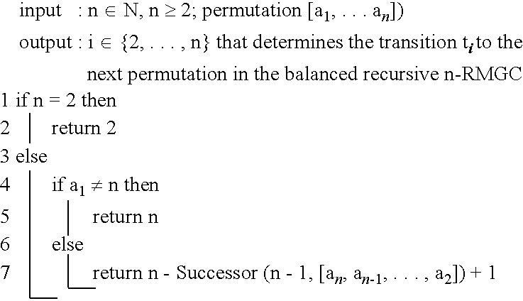 |
The Successor function takes as input the current permutation, and determines the transition ti to the next permutation in the balanced recursive n-RMGC. If n=2, the next transition is always t2 (
the transitions are tn, and these occur whenever the cell n is not the highest charged one, and they are determined in just one step. Of the cases where n is highest charged, by recursion, a fraction
of the transitions are determined by just one more step, and so on. At the basis of the recursion, permutations over two elements require zero steps. Equivalently, the query “is a1 equal to n” is performed for every permutation, therefore n! times; the query “is an equal to n−1” is performed only for
permutations, therefore (n−1)! times, and so on. Thus, the total number of queries is in Σi=3 ni!. Since limn→∞Σi=3 n!/n!=1, the asymptotic average number of steps to generate the next permutation is as stated.
Rank([a 1 , . . . , a n])=((i−2)mod n)+n·Rank([a i−1 , . . . , a 1 , a n , . . . , a i+1]) Equation (1)
| Procedure Factoradic-To-BFactoradic |
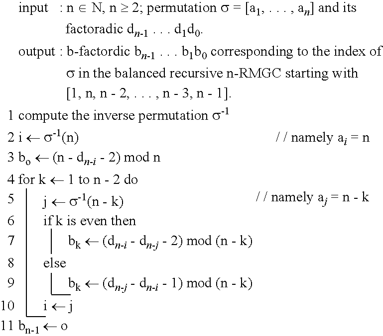 |
| Procedure Unrank |
 |
IV. Rewriting with Rank-Modulation Codes
We will show that a vertex v is in Br n(u) if and only if vεPu.
Since Br n(u)=∪0<=i<=rSi n(u), the second claim follows.
By definition, the number of prefix sequences of length ρ(n, l) is at least l, which allows the first of the construction. To complete the proof, it is obvious from the description of μ that the worst-case rewrite cost of the construction is at most ρ(n, l). By Lemma 16 this is also the best we can hope for.
sets, which induce the mapping:
P 3([1])={[1,2,3][1,3,2]}
P 3([2])={[2,1,3][2,3,1]}
P 3([3])={[3,1,2][3,2,1]}
| a1 = [1] | ||
| a4 = [3, 2] | ||
| a7 = [4, 2] | ||
| a2 = [2] | ||
| a5 = [3, 4] | ||
| a8 = [4, 3, 1] | ||
| a3 = [3, 1] | ||
| a6 = [4, 1] | ||
| a9 = [4, 3, 2] | ||
| TABLE 2 | ||
| P4([1]) = {[1, 2, 3, 4], [1, 2, 4, 3], . . . , [1, 4, 3, 2]} |
||
| P4([2]) = {[2, 1, 3, 4], [2, 1, 4, 3], . . . , [2, 4, 3, 1]} |
||
| P4([3, 1]) = {[3, 1, 2, 4], [3, 1, 4, 2]} |
||
| P4([3, 2]) = {[3, 2, 1, 4], [3, 2, 4, 1]} |
||
| P4([3, 4]) = {[3, 4, 1, 2], [3, 4, 2, 1]} |
||
| P4([4, 1]) = {[4, 1, 2, 3], [4, 1, 3, 2]} |
||
| P4([4, 2]) = {[4, 2, 1, 3], [4, 2, 3, 1]} |
||
| P4([4, 3, 1]) = {[4, 3, 1, 2]} |
||
| P4([4, 3, 2]) = {[4, 3, 2, 1]} |
||
opt1(9,4)=opt2(9−2,(4−2)·3)+(p 8 +p 9).
opt2(7,6)=opt3(7−5,(6−5)·2)+(2p 3+2p 4+2p 5+2p 6+2p 7),
we can determine that there are five leaves in
p1≧p2≧ . . . ≧pl.
Let us denote by s′1, . . . , s′l−1εSn\{si} the l−1 closest permutations to si ordered by increasing distance, i.e.,
α(s i →s′ 1)≦α(s i →s′ 2)≦ . . . ≦α(s i →s′ l−1),
and denote δj=a (si→s′j) for every jε[l−1]. We note that δ1, . . . , δl−1 are independent of the choice of si, and furthermore, that δl=1 while δl−1=ρ(n, l).
Since |ai|>=1=|zi (i)| it follows that
ξA(i)≦3ξ(i). Equation (2)
When n=2, 3, 4, 5, 6, 7, the values of R(n) are
respectively. Thus, R(n)≦1 for all 2≦n≦7. We now show that when n≧8, R(n) monotonically decreases in n. Substituting {rm} into Equation (3) we get
1=|z 1 |≦|z 2 |≦ . . . ≦|z l|.
p1≧p2≧ . . . ≧pl.
that is, for all jε[l],
Note that for all jε[l], the prefix sequence zj (i) represents the information symbol j, which is associated with the probability pj in rewriting.
|z 2 |≦|z 3 |≦ . . . ≦|z l|,
It follows that for every jε[l]≠i,
|z j (i) |=|z skip
Hence, property P.1 holds.
ξA(i)≦3ξ(i),
i.e., the average cost of rewriting i under A is at most three times the lower bound.
Let A′ be a prefix-free code over [l′] which minimizes its average codeword length.
for every iε[l].
ξA(i)≦ξA′(i)
for all iε[l]. By applying inequality (2), and since by Lemma 25 the code Z(i) exists over [l], we get that
ξA(i)≦ξA′(i)≦3ξ′(i)=3ξ(i),
for every iε[l].
ξA(i)≦2ξ(i),
i.e., the average cost of rewriting i under A is at most twice the lower bound.
respectively. Thus, Q(n)≦1 for all 4≦n≦10. We now show that when n≧11, Q(n) monotonically decreases in n. Substituting {qm} into the formula for Q(n) we get
Hence, Q(n) monotonically decreases for all n≧11 which immediately gives us Q(n)≦1 for all n≧4. By
writes. The n/2 cells totally support
writes. When the two variables have different modification frequencies, in the worst case—when all the modifications happen to one of the two variables—the n cells support only
writes, after which a block erasure becomes necessary.
-
- The rows have five types: type-1, type-2, . . . , type-5. The type of a row is determined by the full order of its three index cells. (Three cells can have six orders, so it is doable.) Let's use Sj to denote the set of rows of type-j, where Sj ⊂{1, 2, . . . , a}. For a row—let's say the i-th row—let Ci denote the number of counting cells whose levels are all higher than the reference cell. That is, Ci=|{ci,j|L(c,j)>L(ci,4),5≦j≦b}|.
- The type-1 and type-2 rows (respectively, type-3 and type-4 rows) are used to represent the variable V1 (respectively, V2), as follows:
(mod 3), and
Those type-5 rows represent neither variable.
-
- In each row, if a counting cell's level is higher than the reference cell, we call it set; otherwise, it is un-set. When V1 changes its value, its new value minus its old value equals either 1 or 2 (modulo 3). So to store its new value, we can pick a type-1 or type-2 row and set one more counting cell there. If all the counting cells there are already set, raise the reference cell's level so that those counting cells become un-set again. If the cells in the row have reached the maximum level, change a type-5 row into a type-1 or type-2 row and do the same. Finally, notice that we also have the option of setting two counting cells in a type-1 or type-2 row for a write (if necessary). For variable V2, its value is rewritten in a similar way.
writes, no matter how unevenly the two variables are modified. This can be much better than the separate coding approach when n is sufficiently large. For example, when n>>4, by setting a=b=√{square root over (n)}, the joint coding approach guarantees to support nearly
writes, while the separate coding approach only guarantees nearly
writes. That is a 200% increase in the rewriting performance.
Therefore, joint coding—which generalizes the rank permutation coding—is a potentially very powerful tool to balance cell loads.
times more when n is large.
t i(a 1 , . . . , a i−1 , a i , a i+1 , . . . , a n)=[a i , a 1 , . . . , a i−1 , a i+1 , . . . , a n],
thereby comprising a length-n Rank Modulation Gray Code (n-RMGC) having n! states. As described in previous sections, the n-RMGC can be generated in such a way that it is a cyclic and complete code, or it may be generated so that it is cyclic, complete, and balanced. For a given code generating methodology (i.e., programming operation), the read operations may comprise inverse operations to the code generation. That is, if a particular methodology is used to generate a permutation A given a received data value x for storage, then a reverse set of operations may be carried out to generate a data value x given a permutation A. Such inverse operations will be apparent to those skilled in the art in view of the description herein. Lastly, at
t i(a 1 , . . . , a i−1 , a i , a i+1 , . . . , a n)=[a i , a 1 , . . . , a i−1 , a i+1 , . . . , a n]
thereby comprising a lengthen Rank Modulation Gray Code (n-RMGC) having n! states. In general, raising the charge level of the i-th storage element comprises increasing the stored charge level by a predetermined incremental amount. The precision needed for the incremental amount, however, is greatly reduced over conventional data storage techniques for multi-level cells, because the incremental amount need only be sufficient to distinguish relative ranking of the stored charge level of the storage elements within a virtual cell.
Claims (58)
Priority Applications (1)
| Application Number | Priority Date | Filing Date | Title |
|---|---|---|---|
| US12/275,186 US8245094B2 (en) | 2007-11-20 | 2008-11-20 | Rank modulation for flash memories |
Applications Claiming Priority (3)
| Application Number | Priority Date | Filing Date | Title |
|---|---|---|---|
| US386507P | 2007-11-20 | 2007-11-20 | |
| US1080308P | 2008-01-11 | 2008-01-11 | |
| US12/275,186 US8245094B2 (en) | 2007-11-20 | 2008-11-20 | Rank modulation for flash memories |
Publications (2)
| Publication Number | Publication Date |
|---|---|
| US20090132758A1 US20090132758A1 (en) | 2009-05-21 |
| US8245094B2 true US8245094B2 (en) | 2012-08-14 |
Family
ID=40524950
Family Applications (1)
| Application Number | Title | Priority Date | Filing Date |
|---|---|---|---|
| US12/275,186 Active 2031-03-27 US8245094B2 (en) | 2007-11-20 | 2008-11-20 | Rank modulation for flash memories |
Country Status (2)
| Country | Link |
|---|---|
| US (1) | US8245094B2 (en) |
| WO (1) | WO2009067633A1 (en) |
Cited By (58)
| Publication number | Priority date | Publication date | Assignee | Title |
|---|---|---|---|---|
| US20130121084A1 (en) * | 2011-11-10 | 2013-05-16 | Sandisk Technologies Inc. | Method and apparatus to provide data including hard bit data and soft bit data to a rank modulation decoder |
| US9086955B2 (en) | 2012-03-08 | 2015-07-21 | California Institute Of Technology | Rank-modulation rewriting codes for flash memories |
| US9136015B2 (en) | 2013-04-24 | 2015-09-15 | Apple Inc. | Threshold adjustment using data value balancing in analog memory device |
| US9288089B2 (en) | 2010-04-30 | 2016-03-15 | Ecole Polytechnique Federale De Lausanne (Epfl) | Orthogonal differential vector signaling |
| US9361223B1 (en) | 2012-05-14 | 2016-06-07 | Kandou Labs, S.A. | Storage method and apparatus for random access memory using codeword storage |
| US9362962B2 (en) | 2010-05-20 | 2016-06-07 | Kandou Labs, S.A. | Methods and systems for energy-efficient communications interface |
| US9424908B2 (en) | 2010-12-30 | 2016-08-23 | Kandou Labs, S.A. | Differential vector storage for dynamic random access memory |
| US9450791B2 (en) | 2010-05-20 | 2016-09-20 | Kandoub Lab, S.A. | Circuits for efficient detection of vector signaling codes for chip-to-chip communication |
| US9485057B2 (en) | 2010-05-20 | 2016-11-01 | Kandou Labs, S.A. | Vector signaling with reduced receiver complexity |
| US20160328289A1 (en) * | 2015-05-04 | 2016-11-10 | Texas Instruments Incorporated | Error correction code management of write-once memory codes |
| US9544015B2 (en) | 2014-06-25 | 2017-01-10 | Kandou Labs, S.A. | Multilevel driver for high speed chip-to-chip communications |
| US9577664B2 (en) | 2010-05-20 | 2017-02-21 | Kandou Labs, S.A. | Efficient processing and detection of balanced codes |
| US9607673B1 (en) | 2010-05-20 | 2017-03-28 | Kandou Labs S.A. | Methods and systems for pin-efficient memory controller interface using vector signaling codes for chip-to-chip communication |
| US9667379B2 (en) | 2010-06-04 | 2017-05-30 | Ecole Polytechnique Federale De Lausanne (Epfl) | Error control coding for orthogonal differential vector signaling |
| US9674014B2 (en) | 2014-10-22 | 2017-06-06 | Kandou Labs, S.A. | Method and apparatus for high speed chip-to-chip communications |
| US9686107B2 (en) | 2010-05-20 | 2017-06-20 | Kandou Labs, S.A. | Methods and systems for chip-to-chip communication with reduced simultaneous switching noise |
| US9686106B2 (en) | 2014-02-28 | 2017-06-20 | Kandou Labs, S.A. | Clock-embedded vector signaling codes |
| US9692381B2 (en) | 2014-05-16 | 2017-06-27 | Kandou Labs, S.A. | Symmetric linear equalization circuit with increased gain |
| US9772935B2 (en) | 2014-09-16 | 2017-09-26 | Empire Technology Development Llc | Data storage based on rank modulation in single-level flash memory |
| US9825723B2 (en) | 2010-05-20 | 2017-11-21 | Kandou Labs, S.A. | Methods and systems for skew tolerance in and advanced detectors for vector signaling codes for chip-to-chip communication |
| US9832046B2 (en) | 2015-06-26 | 2017-11-28 | Kandou Labs, S.A. | High speed communications system |
| US9838234B2 (en) | 2014-08-01 | 2017-12-05 | Kandou Labs, S.A. | Orthogonal differential vector signaling codes with embedded clock |
| US9838017B2 (en) | 2010-05-20 | 2017-12-05 | Kandou Labs, S.A. | Methods and systems for high bandwidth chip-to-chip communcations interface |
| US9841918B2 (en) | 2015-12-02 | 2017-12-12 | Samsung Electronics Co., Ltd. | Flash memory device including deduplication, and related methods |
| US9893911B2 (en) | 2014-07-21 | 2018-02-13 | Kandou Labs, S.A. | Multidrop data transfer |
| US9906358B1 (en) | 2016-08-31 | 2018-02-27 | Kandou Labs, S.A. | Lock detector for phase lock loop |
| US9985745B2 (en) | 2013-06-25 | 2018-05-29 | Kandou Labs, S.A. | Vector signaling with reduced receiver complexity |
| US10003315B2 (en) | 2016-01-25 | 2018-06-19 | Kandou Labs S.A. | Voltage sampler driver with enhanced high-frequency gain |
| US10003454B2 (en) | 2016-04-22 | 2018-06-19 | Kandou Labs, S.A. | Sampler with low input kickback |
| US10003424B2 (en) | 2014-07-17 | 2018-06-19 | Kandou Labs, S.A. | Bus reversible orthogonal differential vector signaling codes |
| US10056903B2 (en) | 2016-04-28 | 2018-08-21 | Kandou Labs, S.A. | Low power multilevel driver |
| US10055372B2 (en) | 2015-11-25 | 2018-08-21 | Kandou Labs, S.A. | Orthogonal differential vector signaling codes with embedded clock |
| US10057049B2 (en) | 2016-04-22 | 2018-08-21 | Kandou Labs, S.A. | High performance phase locked loop |
| US10091035B2 (en) | 2013-04-16 | 2018-10-02 | Kandou Labs, S.A. | Methods and systems for high bandwidth communications interface |
| US10116468B1 (en) | 2017-06-28 | 2018-10-30 | Kandou Labs, S.A. | Low power chip-to-chip bidirectional communications |
| US10153591B2 (en) | 2016-04-28 | 2018-12-11 | Kandou Labs, S.A. | Skew-resistant multi-wire channel |
| US10177812B2 (en) | 2014-01-31 | 2019-01-08 | Kandou Labs, S.A. | Methods and systems for reduction of nearest-neighbor crosstalk |
| US10200218B2 (en) | 2016-10-24 | 2019-02-05 | Kandou Labs, S.A. | Multi-stage sampler with increased gain |
| US10200188B2 (en) | 2016-10-21 | 2019-02-05 | Kandou Labs, S.A. | Quadrature and duty cycle error correction in matrix phase lock loop |
| US10203226B1 (en) | 2017-08-11 | 2019-02-12 | Kandou Labs, S.A. | Phase interpolation circuit |
| US10277431B2 (en) | 2016-09-16 | 2019-04-30 | Kandou Labs, S.A. | Phase rotation circuit for eye scope measurements |
| US10320588B2 (en) | 2014-07-10 | 2019-06-11 | Kandou Labs, S.A. | Vector signaling codes with increased signal to noise characteristics |
| US10326623B1 (en) | 2017-12-08 | 2019-06-18 | Kandou Labs, S.A. | Methods and systems for providing multi-stage distributed decision feedback equalization |
| US10333741B2 (en) | 2016-04-28 | 2019-06-25 | Kandou Labs, S.A. | Vector signaling codes for densely-routed wire groups |
| US10333749B2 (en) | 2014-05-13 | 2019-06-25 | Kandou Labs, S.A. | Vector signaling code with improved noise margin |
| US10332593B2 (en) | 2015-09-14 | 2019-06-25 | Toshiba Memory Corporation | Semiconductor memory device configured to sense memory cell threshold voltages in ascending order |
| US10348436B2 (en) | 2014-02-02 | 2019-07-09 | Kandou Labs, S.A. | Method and apparatus for low power chip-to-chip communications with constrained ISI ratio |
| US10372665B2 (en) | 2016-10-24 | 2019-08-06 | Kandou Labs, S.A. | Multiphase data receiver with distributed DFE |
| US10467177B2 (en) | 2017-12-08 | 2019-11-05 | Kandou Labs, S.A. | High speed memory interface |
| US10554380B2 (en) | 2018-01-26 | 2020-02-04 | Kandou Labs, S.A. | Dynamically weighted exclusive or gate having weighted output segments for phase detection and phase interpolation |
| US10666297B2 (en) | 2017-04-14 | 2020-05-26 | Kandou Labs, S.A. | Pipelined forward error correction for vector signaling code channel |
| US10686583B2 (en) | 2017-07-04 | 2020-06-16 | Kandou Labs, S.A. | Method for measuring and correcting multi-wire skew |
| US10693688B2 (en) | 2017-12-28 | 2020-06-23 | Kandou Labs, S.A. | Synchronously-switched multi-input demodulating comparator |
| US10693473B2 (en) | 2017-05-22 | 2020-06-23 | Kandou Labs, S.A. | Multi-modal data-driven clock recovery circuit |
| US10693587B2 (en) | 2017-07-10 | 2020-06-23 | Kandou Labs, S.A. | Multi-wire permuted forward error correction |
| US10756849B2 (en) | 2019-01-21 | 2020-08-25 | Apple Inc. | Self referenced single-ended chip to chip communication |
| US11240076B2 (en) | 2014-05-13 | 2022-02-01 | Kandou Labs, S.A. | Vector signaling code with improved noise margin |
| US11831472B1 (en) | 2022-08-30 | 2023-11-28 | Kandou Labs SA | Pre-scaler for orthogonal differential vector signalling |
Families Citing this family (52)
| Publication number | Priority date | Publication date | Assignee | Title |
|---|---|---|---|---|
| US8365039B2 (en) * | 2008-05-21 | 2013-01-29 | Intel Corporation | Adjustable read reference for non-volatile memory |
| US8276028B2 (en) * | 2008-05-23 | 2012-09-25 | Intel Corporation | Using error information from nearby locations to recover uncorrectable data in non-volatile memory |
| US8732389B2 (en) | 2009-06-23 | 2014-05-20 | Seagate Technology Llc | Memory wear control |
| US8407564B2 (en) * | 2009-07-15 | 2013-03-26 | Intel Corporation | Prediction and cancellation of systematic noise sources in non-volatile memory |
| US9401828B2 (en) | 2010-05-20 | 2016-07-26 | Kandou Labs, S.A. | Methods and systems for low-power and pin-efficient communications with superposition signaling codes |
| US9479369B1 (en) | 2010-05-20 | 2016-10-25 | Kandou Labs, S.A. | Vector signaling codes with high pin-efficiency for chip-to-chip communication and storage |
| US9985634B2 (en) | 2010-05-20 | 2018-05-29 | Kandou Labs, S.A. | Data-driven voltage regulator |
| US9596109B2 (en) | 2010-05-20 | 2017-03-14 | Kandou Labs, S.A. | Methods and systems for high bandwidth communications interface |
| US9106238B1 (en) | 2010-12-30 | 2015-08-11 | Kandou Labs, S.A. | Sorting decoder |
| US9450744B2 (en) | 2010-05-20 | 2016-09-20 | Kandou Lab, S.A. | Control loop management and vector signaling code communications links |
| US9564994B2 (en) | 2010-05-20 | 2017-02-07 | Kandou Labs, S.A. | Fault tolerant chip-to-chip communication with advanced voltage |
| US8880783B2 (en) * | 2011-07-05 | 2014-11-04 | Kandou Labs SA | Differential vector storage for non-volatile memory |
| US9300503B1 (en) | 2010-05-20 | 2016-03-29 | Kandou Labs, S.A. | Methods and systems for skew tolerance in and advanced detectors for vector signaling codes for chip-to-chip communication |
| US8578246B2 (en) | 2010-05-31 | 2013-11-05 | International Business Machines Corporation | Data encoding in solid-state storage devices |
| US8537613B2 (en) | 2011-03-31 | 2013-09-17 | Sandisk Technologies Inc. | Multi-layer memory system |
| US8879319B1 (en) * | 2011-07-29 | 2014-11-04 | Ecole Polytechnique Federale De Lausanne (Epfl) | Re-writing scheme for solid-state storage devices |
| DE112012003458B4 (en) * | 2011-09-29 | 2016-04-07 | International Business Machines Corporation | Read recognition in semiconductor memory units |
| GB2513749B (en) | 2011-12-21 | 2014-12-31 | Ibm | Read/write operations in solid-state storage devices |
| US8699266B2 (en) | 2012-01-30 | 2014-04-15 | HGST Netherlands B.V. | Implementing enhanced data write for multi-level cell (MLC) memory using threshold voltage-drift or resistance drift tolerant moving baseline memory data encoding |
| US8792272B2 (en) | 2012-01-30 | 2014-07-29 | HGST Netherlands B.V. | Implementing enhanced data partial-erase for multi-level cell (MLC) memory using threshold voltage-drift or resistance drift tolerant moving baseline memory data encoding |
| US9208871B2 (en) | 2012-01-30 | 2015-12-08 | HGST Netherlands B.V. | Implementing enhanced data read for multi-level cell (MLC) memory using threshold voltage-drift or resistance drift tolerant moving baseline memory data encoding |
| US9230652B2 (en) * | 2012-03-08 | 2016-01-05 | California Institute Of Technology | Flash memories using minimum push up, multi-cell and multi-permutation schemes for data storage |
| US9265458B2 (en) | 2012-12-04 | 2016-02-23 | Sync-Think, Inc. | Application of smooth pursuit cognitive testing paradigms to clinical drug development |
| US8873284B2 (en) | 2012-12-31 | 2014-10-28 | Sandisk Technologies Inc. | Method and system for program scheduling in a multi-layer memory |
| US9348746B2 (en) | 2012-12-31 | 2016-05-24 | Sandisk Technologies | Method and system for managing block reclaim operations in a multi-layer memory |
| US9734050B2 (en) | 2012-12-31 | 2017-08-15 | Sandisk Technologies Llc | Method and system for managing background operations in a multi-layer memory |
| US9734911B2 (en) | 2012-12-31 | 2017-08-15 | Sandisk Technologies Llc | Method and system for asynchronous die operations in a non-volatile memory |
| US9465731B2 (en) | 2012-12-31 | 2016-10-11 | Sandisk Technologies Llc | Multi-layer non-volatile memory system having multiple partitions in a layer |
| US9223693B2 (en) | 2012-12-31 | 2015-12-29 | Sandisk Technologies Inc. | Memory system having an unequal number of memory die on different control channels |
| US9336133B2 (en) | 2012-12-31 | 2016-05-10 | Sandisk Technologies Inc. | Method and system for managing program cycles including maintenance programming operations in a multi-layer memory |
| US9380976B2 (en) | 2013-03-11 | 2016-07-05 | Sync-Think, Inc. | Optical neuroinformatics |
| US9489294B2 (en) | 2013-06-19 | 2016-11-08 | Sandisk Technologies Llc | Data encoding for non-volatile memory |
| US9117520B2 (en) | 2013-06-19 | 2015-08-25 | Sandisk Technologies Inc. | Data encoding for non-volatile memory |
| US9489300B2 (en) | 2013-06-19 | 2016-11-08 | Sandisk Technologies Llc | Data encoding for non-volatile memory |
| US9489299B2 (en) | 2013-06-19 | 2016-11-08 | Sandisk Technologies Llc | Data encoding for non-volatile memory |
| US9117514B2 (en) | 2013-06-19 | 2015-08-25 | Sandisk Technologies Inc. | Data encoding for non-volatile memory |
| WO2015077608A1 (en) | 2013-11-22 | 2015-05-28 | Kandou Labs SA | Multiwire linear equalizer for vector signaling code receiver |
| GB201320983D0 (en) * | 2013-11-28 | 2014-01-15 | Ibm | Data encoding in solid-state storage apparatus |
| US9390008B2 (en) | 2013-12-11 | 2016-07-12 | Sandisk Technologies Llc | Data encoding for non-volatile memory |
| TWI511136B (en) * | 2014-01-09 | 2015-12-01 | Macronix Int Co Ltd | Memory system and associated access method |
| US9369312B1 (en) | 2014-02-02 | 2016-06-14 | Kandou Labs, S.A. | Low EMI signaling for parallel conductor interfaces |
| US9589654B2 (en) | 2014-04-15 | 2017-03-07 | Empire Technology Development Llc | Rank determination of circuits with distinct current carrying capabilities |
| US9852806B2 (en) | 2014-06-20 | 2017-12-26 | Kandou Labs, S.A. | System for generating a test pattern to detect and isolate stuck faults for an interface using transition coding |
| GB2527604A (en) * | 2014-06-27 | 2015-12-30 | Ibm | Data encoding in solid-state storage devices |
| WO2016094741A1 (en) * | 2014-12-10 | 2016-06-16 | California Institute Of Technology | Improving nand flash reliability with rank modulation |
| US9690517B2 (en) * | 2015-05-22 | 2017-06-27 | Texas Instruments Incorporated | Dual-mode error-correction code/write-once memory codec |
| US9557760B1 (en) | 2015-10-28 | 2017-01-31 | Kandou Labs, S.A. | Enhanced phase interpolation circuit |
| US9577815B1 (en) | 2015-10-29 | 2017-02-21 | Kandou Labs, S.A. | Clock data alignment system for vector signaling code communications link |
| US10133490B2 (en) | 2015-10-30 | 2018-11-20 | Sandisk Technologies Llc | System and method for managing extended maintenance scheduling in a non-volatile memory |
| US10120613B2 (en) | 2015-10-30 | 2018-11-06 | Sandisk Technologies Llc | System and method for rescheduling host and maintenance operations in a non-volatile memory |
| US9778855B2 (en) | 2015-10-30 | 2017-10-03 | Sandisk Technologies Llc | System and method for precision interleaving of data writes in a non-volatile memory |
| US10042553B2 (en) | 2015-10-30 | 2018-08-07 | Sandisk Technologies Llc | Method and system for programming a multi-layer non-volatile memory having a single fold data path |
Citations (7)
| Publication number | Priority date | Publication date | Assignee | Title |
|---|---|---|---|---|
| US2632058A (en) | 1946-03-22 | 1953-03-17 | Bell Telephone Labor Inc | Pulse code communication |
| US3196351A (en) | 1962-06-26 | 1965-07-20 | Bell Telephone Labor Inc | Permutation code signaling |
| US5832493A (en) | 1997-04-24 | 1998-11-03 | Trimble Navigation Limited | Flash file management system |
| US6266279B1 (en) | 2000-02-17 | 2001-07-24 | Mitsubishi Denki Kabushiki Kaisha | Nonvolatile semiconductor memory device, method for reading data from the nonvolatile semiconductor memory device, and method for writing data into the nonvolatile semiconductor memory device |
| US20020118573A1 (en) | 2000-12-29 | 2002-08-29 | Stmicroelectronics S.R.L. | Method for storing data in a nonvolatile memory |
| US6535949B1 (en) | 1999-04-19 | 2003-03-18 | Research In Motion Limited | Portable electronic device having a log-structured file system in flash memory |
| US20050237798A1 (en) | 2004-03-30 | 2005-10-27 | Katsutoshi Urabe | Nonvolatile semiconductor memory device and method of rewriting data thereof |
-
2008
- 2008-11-20 WO PCT/US2008/084249 patent/WO2009067633A1/en active Application Filing
- 2008-11-20 US US12/275,186 patent/US8245094B2/en active Active
Patent Citations (7)
| Publication number | Priority date | Publication date | Assignee | Title |
|---|---|---|---|---|
| US2632058A (en) | 1946-03-22 | 1953-03-17 | Bell Telephone Labor Inc | Pulse code communication |
| US3196351A (en) | 1962-06-26 | 1965-07-20 | Bell Telephone Labor Inc | Permutation code signaling |
| US5832493A (en) | 1997-04-24 | 1998-11-03 | Trimble Navigation Limited | Flash file management system |
| US6535949B1 (en) | 1999-04-19 | 2003-03-18 | Research In Motion Limited | Portable electronic device having a log-structured file system in flash memory |
| US6266279B1 (en) | 2000-02-17 | 2001-07-24 | Mitsubishi Denki Kabushiki Kaisha | Nonvolatile semiconductor memory device, method for reading data from the nonvolatile semiconductor memory device, and method for writing data into the nonvolatile semiconductor memory device |
| US20020118573A1 (en) | 2000-12-29 | 2002-08-29 | Stmicroelectronics S.R.L. | Method for storing data in a nonvolatile memory |
| US20050237798A1 (en) | 2004-03-30 | 2005-10-27 | Katsutoshi Urabe | Nonvolatile semiconductor memory device and method of rewriting data thereof |
Non-Patent Citations (44)
| Title |
|---|
| "SanDisk launches 64 gigabyte solid state drives for notebook PCs, meeting needs for higher capacity," Press Release, Business Wire, Jun. 5, 2007, 5 pages. |
| 2008 IEEE International Symposium on Information Theory (ISIT2008), Toronto, Ontario, Canada, poster, retrieved off the internet at URL http://www.isit2008.org/ on Oct. 20, 2009. |
| Aleph One, "YAFFS: Yet another flash filing system . . . ", Cambridge, UK, 2002, retrieved from the Internet at http://web.archive.org/web/20040217235559/http:/www.aleph1.co.uk/yaffs/index.html as posted on Feb. 17, 2004. The YAFFS material has been moved to www.yaffs.net. |
| Aritome, S. et al., "Reliability issues of flash memory cells", Proceedings of the IEEE, 81(5):776-788 May 1993. |
| Baer, M. B., "Optimal prefix codes for infinite alphabets with nonlinear costs", IEEE Trans. on Inform. Theory, 54(3):1273-1286, Mar. 2008. |
| Berger, T. et al., "Permutation codes for sources", IEEE Trans. on Inform. Theory, IT-18(1):160-169, Jan. 1972. |
| Birrell, A. et al., "A design for high performance flash disks," ACM Operating Systems Review, 41(2):88-93, Apr. 2007. |
| Blaum, M. et al., "Interleaving schemes for multidimensional cluster errors", IEEE Transactions on Information Theory, 44(2):730-743, Mar. 1998. |
| Bohossian, V. et al., "Buffer coding for asymmetric multi-level memory", IEEE International Symposium on Information Theory (ISIT2007), Nice, France, pp. 1186-1190, Jun. 2007. |
| Cappelletti, P. et al., Chapter 5, "Memory Architecture and Related Issues" in Flash memories, Kluwer Academic Publishers, pp. 241-360,1st Edition (1999). |
| Cappelletti, P. et al., Chapter 6, "Multilevel Flash Memories", in Flash Memories, Kluwer Academic Publishers, pp. 361-397, 1st Edition (1999). |
| Cohen, G. D. et al., "Linear binary code for write-once memories", IEEE Trans. on Inform. Theory, IT-32(5):697-700, Sep. 1986. |
| Dan, R. et al., "A TrueFFS® and FLite(TM) technical overview of M-systems' flash file systems", Technical Report 80-SR-002-00-6L Rev. 1.30, Mar. 1997, 14 pages. |
| Dan, R. et al., "A TrueFFS® and FLite™ technical overview of M-systems' flash file systems", Technical Report 80-SR-002-00-6L Rev. 1.30, Mar. 1997, 14 pages. |
| Dietz, P., "Optimal algorithms for list indexing and subset rank", from Lecture Notes in Computer Science, G. Goos, ed., at 39-46, Springer-Verlag London, UK (1989). |
| Douglis, F. et al., Proceedings of the First USENIX Symposium on Operating Systems Design and Implementation (OSDI), pp. 25-37, Monterey, CA, Nov. 14-17, 1994. |
| Fiat, A. et al., "Generalized 'write-once' memories", IEEE Trans. on Inform. Theory, IT-30(3):470-480, May 1984. |
| Fu, F. et al., "On the capacity of generalized write-once memory with state transitions described by an arbitrary directed acyclic graph," 45(1):308-313, Jan. 1999. |
| Gal, E. et al., "Algorithms and data structures for flash memories", ACM Computing Surveys, 37(2):138-163, Jun. 2005. |
| Golin, M. J. et al., "A dynamic programming algorithm for constructing optimal prefix-free codes with unequal letter costs", IEEE Trans. on Inform. Theory, 44(5):1770-1781, Sep. 1998. |
| Golomb, S. W. et al., "Perfect codes in the Lee metric and the packing of polyominoes", SIAM J. Appl. Math., 18(2):302-317, Jan. 1970. |
| Hall, M. Jr. et al., "Combinatorial analysis and computers", Amer. Math. Monthly, 72(2):21-28, (1965). |
| Heegard, C. et al., "On the capacity of computer memory with defects", IEEE Trans. on Inform. Theory, IT-29(5):731-739, (Sep. 1983). |
| Heegard, C., "On the capacity of permanent memory", IEEE Trans. on Inform. Theory, IT-31(1):34-42, Jan. 1985. |
| Huffman, D. A. "A method for the construction of minimum-redundancy codes", Proceedings of the Institute of Radio Engineers, 40(9):1098-1101, Sep. 1952. |
| Hwang, F. K., "Generalized Huffman trees", SIAM J. Appl. Math., 37(1):124-127, Aug. 1979. |
| International Search Report dated Apr. 29, 2009 for PCT application No. PCT/US2008/084249. |
| Jiang, A. et al., "Floating codes for joint information storage in write asymmetric memories", Proceedings of the 2007 IEEE International Symposium on Information Theory (ISIT2007), Nice, France, pp. 1166-1170, Jun. 2007. |
| Jiang, A. et al., "Joint coding for flash memory storage", Proceedings of the 2008 IEEE International Symposium on Information Theory (ISIT2008), Toronto, Canada, pp. 1741-1745, Jul. 6-11, 2008. |
| Jiang, A., "On the generalization of error-correcting WOM codes", Proceedings of the 2007 IEEE International Symposium on Information Theory (ISIT2007), Nice, France, pp. 1391-1395, Jun. 2007. |
| Knuth, D. E., "The art of computer programming", vol. 3: Sorting and Searching, Addison Wesley, Reading, MA, 2nd ed., (1998), Section 5.2.4 at pp. 158-168, Section 6.2.2 at pp. 426-448. |
| Kuznetsov, A. et al., "On the general defective channel with informed encoder and capacities of some constrained memories", IEEE Trans. on Inform. Theory, 40(6):1866-1871, Nov. 1994. |
| Lehmer, D. H., "Teaching combinatorial tricks to a computer", Proc. Sympos. Appl. Math. Combinatorial Analysis, 10:179-193 (1960). |
| Mares, M. et al., "Linear-time ranking of permutations", Algorithms-ESA, pp. 187-193 (2007). |
| Myrvold, W. et al., "Ranking and unranking permutations in linear time", Information Processing Letters, 79(6):1-6, Apr. 13, 2000. |
| Orlov, S. et al., "Error correcting sparse permutation channel codes for digital holographic data storage", Proceeding of the SPIE, The International Society for Optical Engineering, vol. 6620, May 20, 2007, pp. 662026-1-662026-8. |
| Pavan, P. et al., "Flash memory cells-an overview", Proceedings of the IEEE, 85(8):1248-1271, Aug. 1997. |
| Rivest, R. L. et al., "How to reuse a 'write-once' memory", Information and Control, 55:1-19 (1982). |
| Savage, "A survey of combinatorial gray codes," SIAM Review, vol. 39, No. 4, pp. 605-629, Dec. 1997. |
| Sedgewick, R., "Permutation generation methods", Computing Surveys, 9(2):137-164, Jun. 1977. |
| Slepian, D., "Permutation modulation", Proc. of the IEEE, 53(3):228-236 (1965). |
| Web article entitled "PQI unveils 256GB solid state drive," retrieved from the Internet at URL http://web.archive.org/web/20070603192642/www.guru3d.com/news.html as posted on Jun. 4, 2007. |
| Wolf, J. K. et al., "Coding for a write-once memory", AT&T Bell Laboratories Technical Journal 63(6):1089-1112, Jul.-Aug. 1984. |
| Woodhouse, D., "JFFS: The journaling flash file system," Ottawa Linux Symposium, 2001, 12 pages. |
Cited By (110)
| Publication number | Priority date | Publication date | Assignee | Title |
|---|---|---|---|---|
| US10985806B2 (en) | 2010-04-30 | 2021-04-20 | ECOLE POLYTECHNIQUE FéDéRALE DE LAUSANNE | Orthogonal differential vector signaling |
| US11611377B2 (en) | 2010-04-30 | 2023-03-21 | Ecole Polytechnique Federale De Lausanne | Orthogonal differential vector signaling |
| US10355756B2 (en) | 2010-04-30 | 2019-07-16 | ECOLE POLYTECHNIQUE FéDéRALE DE LAUSANNE | Orthogonal differential vector signaling |
| US9825677B2 (en) | 2010-04-30 | 2017-11-21 | ECOLE POLYTECHNIQUE FéDéRALE DE LAUSANNE | Orthogonal differential vector signaling |
| US9288089B2 (en) | 2010-04-30 | 2016-03-15 | Ecole Polytechnique Federale De Lausanne (Epfl) | Orthogonal differential vector signaling |
| US9825723B2 (en) | 2010-05-20 | 2017-11-21 | Kandou Labs, S.A. | Methods and systems for skew tolerance in and advanced detectors for vector signaling codes for chip-to-chip communication |
| US10044452B2 (en) | 2010-05-20 | 2018-08-07 | Kandou Labs, S.A. | Methods and systems for skew tolerance in and advanced detectors for vector signaling codes for chip-to-chip communication |
| US9838017B2 (en) | 2010-05-20 | 2017-12-05 | Kandou Labs, S.A. | Methods and systems for high bandwidth chip-to-chip communcations interface |
| US9450791B2 (en) | 2010-05-20 | 2016-09-20 | Kandoub Lab, S.A. | Circuits for efficient detection of vector signaling codes for chip-to-chip communication |
| US9485057B2 (en) | 2010-05-20 | 2016-11-01 | Kandou Labs, S.A. | Vector signaling with reduced receiver complexity |
| US9819522B2 (en) | 2010-05-20 | 2017-11-14 | Kandou Labs, S.A. | Circuits for efficient detection of vector signaling codes for chip-to-chip communication |
| US10468078B2 (en) | 2010-05-20 | 2019-11-05 | Kandou Labs, S.A. | Methods and systems for pin-efficient memory controller interface using vector signaling codes for chip-to-chip communication |
| US9362962B2 (en) | 2010-05-20 | 2016-06-07 | Kandou Labs, S.A. | Methods and systems for energy-efficient communications interface |
| US9577664B2 (en) | 2010-05-20 | 2017-02-21 | Kandou Labs, S.A. | Efficient processing and detection of balanced codes |
| US9607673B1 (en) | 2010-05-20 | 2017-03-28 | Kandou Labs S.A. | Methods and systems for pin-efficient memory controller interface using vector signaling codes for chip-to-chip communication |
| US9692555B2 (en) | 2010-05-20 | 2017-06-27 | Kandou Labs, S.A. | Vector signaling with reduced receiver complexity |
| US9686107B2 (en) | 2010-05-20 | 2017-06-20 | Kandou Labs, S.A. | Methods and systems for chip-to-chip communication with reduced simultaneous switching noise |
| US9667379B2 (en) | 2010-06-04 | 2017-05-30 | Ecole Polytechnique Federale De Lausanne (Epfl) | Error control coding for orthogonal differential vector signaling |
| US9424908B2 (en) | 2010-12-30 | 2016-08-23 | Kandou Labs, S.A. | Differential vector storage for dynamic random access memory |
| US10164809B2 (en) | 2010-12-30 | 2018-12-25 | Kandou Labs, S.A. | Circuits for efficient detection of vector signaling codes for chip-to-chip communication |
| US20130121084A1 (en) * | 2011-11-10 | 2013-05-16 | Sandisk Technologies Inc. | Method and apparatus to provide data including hard bit data and soft bit data to a rank modulation decoder |
| US8456919B1 (en) * | 2011-11-10 | 2013-06-04 | Sandisk Technologies Inc. | Method and apparatus to provide data including hard bit data and soft bit data to a rank modulation decoder |
| US9916197B2 (en) | 2012-03-08 | 2018-03-13 | California Institute Of Technology | Rank-modulation rewriting codes for flash memories |
| US9086955B2 (en) | 2012-03-08 | 2015-07-21 | California Institute Of Technology | Rank-modulation rewriting codes for flash memories |
| US9524106B1 (en) | 2012-05-14 | 2016-12-20 | Kandou Labs, S.A. | Storage method and apparatus for random access memory using codeword storage |
| US9361223B1 (en) | 2012-05-14 | 2016-06-07 | Kandou Labs, S.A. | Storage method and apparatus for random access memory using codeword storage |
| US11374801B2 (en) | 2013-04-16 | 2022-06-28 | Kandou Labs, S.A. | Methods and systems for high bandwidth communications interface |
| US10091035B2 (en) | 2013-04-16 | 2018-10-02 | Kandou Labs, S.A. | Methods and systems for high bandwidth communications interface |
| US9136015B2 (en) | 2013-04-24 | 2015-09-15 | Apple Inc. | Threshold adjustment using data value balancing in analog memory device |
| US9985745B2 (en) | 2013-06-25 | 2018-05-29 | Kandou Labs, S.A. | Vector signaling with reduced receiver complexity |
| US10177812B2 (en) | 2014-01-31 | 2019-01-08 | Kandou Labs, S.A. | Methods and systems for reduction of nearest-neighbor crosstalk |
| US10348436B2 (en) | 2014-02-02 | 2019-07-09 | Kandou Labs, S.A. | Method and apparatus for low power chip-to-chip communications with constrained ISI ratio |
| US11683113B2 (en) | 2014-02-02 | 2023-06-20 | Kandou Labs, S.A. | Method and apparatus for low power chip-to-chip communications with constrained ISI ratio |
| US11025359B2 (en) | 2014-02-02 | 2021-06-01 | Kandou Labs, S.A. | Method and apparatus for low power chip-to-chip communications with constrained ISI ratio |
| US10805129B2 (en) | 2014-02-28 | 2020-10-13 | Kandou Labs, S.A. | Clock-embedded vector signaling codes |
| US10374846B2 (en) | 2014-02-28 | 2019-08-06 | Kandou Labs, S.A. | Clock-embedded vector signaling codes |
| US9686106B2 (en) | 2014-02-28 | 2017-06-20 | Kandou Labs, S.A. | Clock-embedded vector signaling codes |
| US10020966B2 (en) | 2014-02-28 | 2018-07-10 | Kandou Labs, S.A. | Vector signaling codes with high pin-efficiency for chip-to-chip communication and storage |
| US10333749B2 (en) | 2014-05-13 | 2019-06-25 | Kandou Labs, S.A. | Vector signaling code with improved noise margin |
| US11716227B2 (en) | 2014-05-13 | 2023-08-01 | Kandou Labs, S.A. | Vector signaling code with improved noise margin |
| US11240076B2 (en) | 2014-05-13 | 2022-02-01 | Kandou Labs, S.A. | Vector signaling code with improved noise margin |
| US9692381B2 (en) | 2014-05-16 | 2017-06-27 | Kandou Labs, S.A. | Symmetric linear equalization circuit with increased gain |
| US9917711B2 (en) | 2014-06-25 | 2018-03-13 | Kandou Labs, S.A. | Multilevel driver for high speed chip-to-chip communications |
| US10091033B2 (en) | 2014-06-25 | 2018-10-02 | Kandou Labs, S.A. | Multilevel driver for high speed chip-to-chip communications |
| US9544015B2 (en) | 2014-06-25 | 2017-01-10 | Kandou Labs, S.A. | Multilevel driver for high speed chip-to-chip communications |
| US10320588B2 (en) | 2014-07-10 | 2019-06-11 | Kandou Labs, S.A. | Vector signaling codes with increased signal to noise characteristics |
| US10404394B2 (en) | 2014-07-17 | 2019-09-03 | Kandou Labs, S.A. | Bus reversible orthogonal differential vector signaling codes |
| US10003424B2 (en) | 2014-07-17 | 2018-06-19 | Kandou Labs, S.A. | Bus reversible orthogonal differential vector signaling codes |
| US9893911B2 (en) | 2014-07-21 | 2018-02-13 | Kandou Labs, S.A. | Multidrop data transfer |
| US10230549B2 (en) | 2014-07-21 | 2019-03-12 | Kandou Labs, S.A. | Multidrop data transfer |
| US9838234B2 (en) | 2014-08-01 | 2017-12-05 | Kandou Labs, S.A. | Orthogonal differential vector signaling codes with embedded clock |
| US10122561B2 (en) | 2014-08-01 | 2018-11-06 | Kandou Labs, S.A. | Orthogonal differential vector signaling codes with embedded clock |
| US10652067B2 (en) | 2014-08-01 | 2020-05-12 | Kandou Labs, S.A. | Orthogonal differential vector signaling codes with embedded clock |
| US9772935B2 (en) | 2014-09-16 | 2017-09-26 | Empire Technology Development Llc | Data storage based on rank modulation in single-level flash memory |
| US9983991B2 (en) | 2014-09-16 | 2018-05-29 | Empire Technology Development Llc | Data storage based on rank modulation in single-level flash memory |
| US10243765B2 (en) | 2014-10-22 | 2019-03-26 | Kandou Labs, S.A. | Method and apparatus for high speed chip-to-chip communications |
| US9674014B2 (en) | 2014-10-22 | 2017-06-06 | Kandou Labs, S.A. | Method and apparatus for high speed chip-to-chip communications |
| US9772899B2 (en) * | 2015-05-04 | 2017-09-26 | Texas Instruments Incorporated | Error correction code management of write-once memory codes |
| US10191801B2 (en) * | 2015-05-04 | 2019-01-29 | Texas Instruments Incorporated | Error correction code management of write-once memory codes |
| US20180011757A1 (en) * | 2015-05-04 | 2018-01-11 | Texas Instruments Incorporated | Error correction code management of write-once memory codes |
| US20160328289A1 (en) * | 2015-05-04 | 2016-11-10 | Texas Instruments Incorporated | Error correction code management of write-once memory codes |
| US10608850B2 (en) | 2015-06-26 | 2020-03-31 | Kandou Labs, S.A. | High speed communications system |
| US11115249B2 (en) | 2015-06-26 | 2021-09-07 | Kandou Labs, S.A. | High speed communications system |
| US10116472B2 (en) | 2015-06-26 | 2018-10-30 | Kandou Labs, S.A. | High speed communications system |
| US11863358B2 (en) | 2015-06-26 | 2024-01-02 | Kandou Labs, S.A. | High speed communications system |
| US9832046B2 (en) | 2015-06-26 | 2017-11-28 | Kandou Labs, S.A. | High speed communications system |
| US10819541B2 (en) | 2015-06-26 | 2020-10-27 | Kandou Labs, S.A. | High speed communications system |
| US10382235B2 (en) | 2015-06-26 | 2019-08-13 | Kandou Labs, S.A. | High speed communications system |
| US11483187B2 (en) | 2015-06-26 | 2022-10-25 | Kandou Labs, S.A. | High speed communications system |
| US10332593B2 (en) | 2015-09-14 | 2019-06-25 | Toshiba Memory Corporation | Semiconductor memory device configured to sense memory cell threshold voltages in ascending order |
| US10324876B2 (en) | 2015-11-25 | 2019-06-18 | Kandou Labs, S.A. | Orthogonal differential vector signaling codes with embedded clock |
| US10055372B2 (en) | 2015-11-25 | 2018-08-21 | Kandou Labs, S.A. | Orthogonal differential vector signaling codes with embedded clock |
| US9841918B2 (en) | 2015-12-02 | 2017-12-12 | Samsung Electronics Co., Ltd. | Flash memory device including deduplication, and related methods |
| US10003315B2 (en) | 2016-01-25 | 2018-06-19 | Kandou Labs S.A. | Voltage sampler driver with enhanced high-frequency gain |
| US10003454B2 (en) | 2016-04-22 | 2018-06-19 | Kandou Labs, S.A. | Sampler with low input kickback |
| US10057049B2 (en) | 2016-04-22 | 2018-08-21 | Kandou Labs, S.A. | High performance phase locked loop |
| US10333741B2 (en) | 2016-04-28 | 2019-06-25 | Kandou Labs, S.A. | Vector signaling codes for densely-routed wire groups |
| US10056903B2 (en) | 2016-04-28 | 2018-08-21 | Kandou Labs, S.A. | Low power multilevel driver |
| US10153591B2 (en) | 2016-04-28 | 2018-12-11 | Kandou Labs, S.A. | Skew-resistant multi-wire channel |
| US10355852B2 (en) | 2016-08-31 | 2019-07-16 | Kandou Labs, S.A. | Lock detector for phase lock loop |
| US9906358B1 (en) | 2016-08-31 | 2018-02-27 | Kandou Labs, S.A. | Lock detector for phase lock loop |
| US10277431B2 (en) | 2016-09-16 | 2019-04-30 | Kandou Labs, S.A. | Phase rotation circuit for eye scope measurements |
| US10200188B2 (en) | 2016-10-21 | 2019-02-05 | Kandou Labs, S.A. | Quadrature and duty cycle error correction in matrix phase lock loop |
| US10372665B2 (en) | 2016-10-24 | 2019-08-06 | Kandou Labs, S.A. | Multiphase data receiver with distributed DFE |
| US10200218B2 (en) | 2016-10-24 | 2019-02-05 | Kandou Labs, S.A. | Multi-stage sampler with increased gain |
| US10666297B2 (en) | 2017-04-14 | 2020-05-26 | Kandou Labs, S.A. | Pipelined forward error correction for vector signaling code channel |
| US11336302B2 (en) | 2017-04-14 | 2022-05-17 | Kandou Labs, S.A. | Pipelined forward error correction for vector signaling code channel |
| US11804855B2 (en) | 2017-04-14 | 2023-10-31 | Kandou Labs, S.A. | Pipelined forward error correction for vector signaling code channel |
| US11804845B2 (en) | 2017-05-22 | 2023-10-31 | Kandou Labs, S.A. | Multi-modal data-driven clock recovery circuit |
| US11271571B2 (en) | 2017-05-22 | 2022-03-08 | Kandou Labs, S.A. | Multi-modal data-driven clock recovery circuit |
| US10693473B2 (en) | 2017-05-22 | 2020-06-23 | Kandou Labs, S.A. | Multi-modal data-driven clock recovery circuit |
| US11032110B2 (en) | 2017-06-28 | 2021-06-08 | Kandou Labs, S.A. | Low power chip-to-chip bidirectional communications |
| US10581644B2 (en) | 2017-06-28 | 2020-03-03 | Kandou Labs, S.A. | Low power chip-to-chip bidirectional communications |
| US11477055B2 (en) | 2017-06-28 | 2022-10-18 | Kandou Labs, S.A. | Low power chip-to-chip bidirectional communications |
| US10116468B1 (en) | 2017-06-28 | 2018-10-30 | Kandou Labs, S.A. | Low power chip-to-chip bidirectional communications |
| US10686583B2 (en) | 2017-07-04 | 2020-06-16 | Kandou Labs, S.A. | Method for measuring and correcting multi-wire skew |
| US11368247B2 (en) | 2017-07-10 | 2022-06-21 | Kandou Labs, S.A. | Multi-wire permuted forward error correction |
| US10693587B2 (en) | 2017-07-10 | 2020-06-23 | Kandou Labs, S.A. | Multi-wire permuted forward error correction |
| US11894926B2 (en) | 2017-07-10 | 2024-02-06 | Kandou Labs, S.A. | Interleaved forward error correction over multiple transport channels |
| US10203226B1 (en) | 2017-08-11 | 2019-02-12 | Kandou Labs, S.A. | Phase interpolation circuit |
| US10467177B2 (en) | 2017-12-08 | 2019-11-05 | Kandou Labs, S.A. | High speed memory interface |
| US10326623B1 (en) | 2017-12-08 | 2019-06-18 | Kandou Labs, S.A. | Methods and systems for providing multi-stage distributed decision feedback equalization |
| US11894961B2 (en) | 2017-12-28 | 2024-02-06 | Kandou Labs, S.A. | Synchronously-switched multi-input demodulating comparator |
| US11469931B2 (en) | 2017-12-28 | 2022-10-11 | Kandou Labs, S.A. | Synchronously-switched multi-input demodulating comparator |
| US11063799B2 (en) | 2017-12-28 | 2021-07-13 | Kandou Labs, S.A. | Synchronously-switched multi-input demodulating comparator |
| US10693688B2 (en) | 2017-12-28 | 2020-06-23 | Kandou Labs, S.A. | Synchronously-switched multi-input demodulating comparator |
| US10554380B2 (en) | 2018-01-26 | 2020-02-04 | Kandou Labs, S.A. | Dynamically weighted exclusive or gate having weighted output segments for phase detection and phase interpolation |
| US11750325B2 (en) | 2019-01-21 | 2023-09-05 | Apple Inc. | Self referenced single-ended chip to chip communication |
| US10756849B2 (en) | 2019-01-21 | 2020-08-25 | Apple Inc. | Self referenced single-ended chip to chip communication |
| US11831472B1 (en) | 2022-08-30 | 2023-11-28 | Kandou Labs SA | Pre-scaler for orthogonal differential vector signalling |
Also Published As
| Publication number | Publication date |
|---|---|
| WO2009067633A1 (en) | 2009-05-28 |
| US20090132758A1 (en) | 2009-05-21 |
Similar Documents
| Publication | Publication Date | Title |
|---|---|---|
| US8245094B2 (en) | Rank modulation for flash memories | |
| Jiang et al. | Rank modulation for flash memories | |
| US8225180B2 (en) | Error correcting codes for rank modulation | |
| US8780620B2 (en) | Information representation and coding for nonvolatile memories | |
| US9916197B2 (en) | Rank-modulation rewriting codes for flash memories | |
| US9666280B2 (en) | Flash memories using minimum push up, multi-cell and multi-permutation schemes for data storage | |
| Jiang et al. | Floating codes for joint information storage in write asymmetric memories | |
| US9632866B2 (en) | Systems for and methods of extending lifetime of non-volatile memory | |
| Jiang et al. | Error-correcting codes for rank modulation | |
| Jiang et al. | Joint coding for flash memory storage | |
| US20080168320A1 (en) | Codes For Limited Magnitude Asymetric Errors In Flash Memories | |
| US9983808B2 (en) | NAND flash reliability with rank modulation | |
| Jiang et al. | Rewriting codes for joint information storage in flash memories | |
| EP0108053A1 (en) | Method and apparatus for reusing non-erasable memory media | |
| Yaakobi et al. | Multidimensional flash codes | |
| Jacobvitz et al. | Writing cosets of a convolutional code to increase the lifetime of flash memory | |
| Gad et al. | Compressed encoding for rank modulation | |
| Kazemi et al. | A geometric view of the service rates of codes problem and its application to the service rate of the first order Reed-Muller codes | |
| Liu et al. | Shaping codes for structured data | |
| Yaakobi et al. | When do WOM codes improve the erasure factor in flash memories? | |
| Gad et al. | Rank-modulation rewrite coding for flash memories | |
| Jagmohan et al. | Coding for multilevel heterogeneous memories | |
| Jiang et al. | Information representation and coding for flash memories | |
| Jiang et al. | Data representation for flash memories | |
| US6088261A (en) | Semiconductor storage device |
Legal Events
| Date | Code | Title | Description |
|---|---|---|---|
| AS | Assignment |
Owner name: CALIFORNIA INSTITUTE OF TECHNOLOGY, CALIFORNIA Free format text: ASSIGNMENT OF ASSIGNORS INTEREST;ASSIGNORS:JIANG, ANXIAO ANDREW;MATEESCU, ROBERT;SCHWARTZ, MOSHE;AND OTHERS;REEL/FRAME:022206/0660;SIGNING DATES FROM 20081209 TO 20090120 Owner name: CALIFORNIA INSTITUTE OF TECHNOLOGY, CALIFORNIA Free format text: ASSIGNMENT OF ASSIGNORS INTEREST;ASSIGNORS:JIANG, ANXIAO ANDREW;MATEESCU, ROBERT;SCHWARTZ, MOSHE;AND OTHERS;SIGNING DATES FROM 20081209 TO 20090120;REEL/FRAME:022206/0660 |
|
| AS | Assignment |
Owner name: TEXAS A & M UNIVERSITY SYSTEM, TEXAS Free format text: CORRECTIVE ASSIGNMENT TO CORRECT THE ASSIGNEE NAME PREVIOUSLY RECORDED ON REEL 022206 FRAME 0660. ASSIGNOR(S) HEREBY CONFIRMS THE PREVIOUS ASSIGNMENT INCORRECTLY LIST CIT AS THE ASSIGNEE. TEXAS A&M IS THE CORRECT ASSIGNEE. THE CORRECT ASSIGNMENT IS ATTACHED.;ASSIGNOR:JIANG, ANXIAO;REEL/FRAME:026565/0629 Effective date: 20101017 |
|
| STCF | Information on status: patent grant |
Free format text: PATENTED CASE |
|
| FPAY | Fee payment |
Year of fee payment: 4 |
|
| MAFP | Maintenance fee payment |
Free format text: PAYMENT OF MAINTENANCE FEE, 8TH YR, SMALL ENTITY (ORIGINAL EVENT CODE: M2552); ENTITY STATUS OF PATENT OWNER: SMALL ENTITY Year of fee payment: 8 |
|
| FEPP | Fee payment procedure |
Free format text: MAINTENANCE FEE REMINDER MAILED (ORIGINAL EVENT CODE: REM.); ENTITY STATUS OF PATENT OWNER: SMALL ENTITY |