US8247971B1 - Resistively heated small planar filament - Google Patents
Resistively heated small planar filament Download PDFInfo
- Publication number
- US8247971B1 US8247971B1 US13/209,862 US201113209862A US8247971B1 US 8247971 B1 US8247971 B1 US 8247971B1 US 201113209862 A US201113209862 A US 201113209862A US 8247971 B1 US8247971 B1 US 8247971B1
- Authority
- US
- United States
- Prior art keywords
- planar
- filament
- planar filament
- pair
- bonding pads
- Prior art date
- Legal status (The legal status is an assumption and is not a legal conclusion. Google has not performed a legal analysis and makes no representation as to the accuracy of the status listed.)
- Expired - Fee Related
Links
Images


Classifications
-
- H—ELECTRICITY
- H01—ELECTRIC ELEMENTS
- H01J—ELECTRIC DISCHARGE TUBES OR DISCHARGE LAMPS
- H01J1/00—Details of electrodes, of magnetic control means, of screens, or of the mounting or spacing thereof, common to two or more basic types of discharge tubes or lamps
- H01J1/02—Main electrodes
- H01J1/13—Solid thermionic cathodes
- H01J1/15—Cathodes heated directly by an electric current
- H01J1/16—Cathodes heated directly by an electric current characterised by the shape
-
- H—ELECTRICITY
- H01—ELECTRIC ELEMENTS
- H01J—ELECTRIC DISCHARGE TUBES OR DISCHARGE LAMPS
- H01J1/00—Details of electrodes, of magnetic control means, of screens, or of the mounting or spacing thereof, common to two or more basic types of discharge tubes or lamps
- H01J1/02—Main electrodes
- H01J1/13—Solid thermionic cathodes
- H01J1/15—Cathodes heated directly by an electric current
- H01J1/18—Supports; Vibration-damping arrangements
-
- H—ELECTRICITY
- H01—ELECTRIC ELEMENTS
- H01J—ELECTRIC DISCHARGE TUBES OR DISCHARGE LAMPS
- H01J35/00—X-ray tubes
- H01J35/02—Details
- H01J35/04—Electrodes ; Mutual position thereof; Constructional adaptations therefor
- H01J35/06—Cathodes
- H01J35/064—Details of the emitter, e.g. material or structure
-
- H—ELECTRICITY
- H01—ELECTRIC ELEMENTS
- H01K—ELECTRIC INCANDESCENT LAMPS
- H01K1/00—Details
- H01K1/02—Incandescent bodies
- H01K1/14—Incandescent bodies characterised by the shape
-
- H—ELECTRICITY
- H01—ELECTRIC ELEMENTS
- H01J—ELECTRIC DISCHARGE TUBES OR DISCHARGE LAMPS
- H01J2201/00—Electrodes common to discharge tubes
- H01J2201/28—Heaters for thermionic cathodes
- H01J2201/2803—Characterised by the shape or size
- H01J2201/2853—Serpentine
- H01J2201/2857—Serpentine being coiled
-
- H—ELECTRICITY
- H01—ELECTRIC ELEMENTS
- H01J—ELECTRIC DISCHARGE TUBES OR DISCHARGE LAMPS
- H01J2201/00—Electrodes common to discharge tubes
- H01J2201/28—Heaters for thermionic cathodes
- H01J2201/2803—Characterised by the shape or size
- H01J2201/2867—Spiral or helix
- H01J2201/2871—Spiral or helix being flattened
Definitions
- Filaments are used to produce light and electrons.
- an alternating current can heat a wire filament formed in a coiled cylindrical or helical loop. Due to the high temperature of the filament, and due to a large bias voltage between the filament and an anode, electrons are emitted from the filament and accelerated towards the anode. These electrons form an electron beam.
- the location where the electron beam impinges on the anode is called the “electron spot.” It can be desirable that this spot be circular with a very small diameter. It can be desirable that this spot be in the same location on the anode in every x-ray tube that is manufactured.
- the shape and placement of the filament in the x-ray tube affects the shape of the spot.
- Some filaments are very small, especially in portable x-ray tubes. Placing such small filaments, in precisely the same location, in every x-ray tube, can be a significant manufacturing challenge. Lack of precision of filament placement during manufacturing can result in an electron spot that is in different locations on the anode in different x-ray tubes. Placement of the filament also affects spot size and shape. Lack of precision of filament placement also results in non-circular spots and spots that are larger than desirable.
- FIGS. 13-14 Shown in FIGS. 13-14 is a coiled cylindrical or helical wire filament 130 .
- the filament 130 heats and cools, the filament 130 can bend and change its shape, as shown in FIG. 14 .
- the electron spot can change both location and size. This can result in variability of x-ray tube performance over time. It is important that the shape and material of the filament allow for long filament life without filament deformation. Also, the coiled cylindrical or helical shape of the filament can result in non-circular electron spots.
- a filament wire with a consistent wire diameter, can be hottest at the mid-point 131 along the length of the wire. If there is a consistent wire diameter, the voltage drop or power loss is consistent along the wire, resulting in the same heat generation rate along the wire.
- the connections at the ends of the wire 132 essentially form a heat sink, allowing more heat dissipation, and cooler temperatures, at the each end of the wire.
- the mid-point of the wire 131 loses less heat by conduction than the wire ends and can be the hottest location on the filament wire. This high heat at the mid-point 131 can result in more rapid deterioration at the wire mid-point 131 .
- this mid-point 131 deteriorates, its diameter decreases, resulting in a larger power loss, higher temperatures, and an even greater rate of deterioration at this location. Due to the higher temperatures and more rapid wire deterioration at the mid-point 131 of the filament wire, most failures occur at this location. Such failures result in decreased tube life and decreased x-ray tube reliability.
- the present invention is directed to an electron emitter comprising a pair of spaced-apart bonding pads configured to receive an electrical connection and an elongated planar filament extending between the pair of bonding pads in a planar layer, the planar filament configured to receive an applied electric current therethrough.
- the planar filament is substantially flat with planar top and bottom surfaces.
- the planar filament has a length and a width in the planar layer transverse to the length.
- planar filament winds in an arcuate path in the planar layer between the pair of bonding pads defining a central spiral segment with the planar filament forming at least one complete revolution about an axis at a center of the planar filament, on either side of the axis, the planar filament forming a double spiral shape oriented parallel to the layer and a pair of serpentine segments on different opposite sides of the spiral segment with each serpentine segment including at least one change in direction.
- the planar filament is continuous and uninterrupted across the width along an entire length of the planar filament and defines a single current path along the length between the pair of bonding pads.
- the planar filament has a non-uniform width measured in a plane of the layer and transverse to a length of the planar filament, including a wider, intermediate portion having a wider width that is greater than narrower portions on opposite ends of the intermediate portion, the wider width being at least twice as wide as the narrower portions, and the wider portion is disposed substantially at the axis at the center of the planar filament.
- This planar design allows for improved electron beam shaping.
- the double spiral-serpentine shape allows for improved strength and stability.
- the uninterrupted width, and the wider intermediate portion allow for increased filament strength and increased lifetime.
- the present invention is directed to a filament device comprising a pair of spaced-apart bonding pads configured to receive an electrical connection and an elongated planar filament extending between the pair of bonding pads in a planar layer.
- the planar filament is substantially flat with planar top and bottom surfaces.
- the planar filament has a length and a width in the planar layer transverse to the length.
- the planar filament is continuous and uninterrupted, across the width along an entire length of the planar filament and defining a single current path along the length between the pair of bonding pads.
- An intermediate portion of the planar filament has a wider width that is greater than narrower portions on opposite ends of the intermediate portion, the wider width is at least two times wider than narrower portions.
- This planar design allows for improved electron beam, or electromagnetic radiation, shaping.
- the uninterrupted width, and the wider intermediate portion allow for increased filament strength and increased filament lifetime.
- the present invention is directed to a filament device comprising a pair of spaced-apart bonding pads configured to receive an electrical connection and an elongated planar filament extending between the pair of bonding pads in a planar layer.
- the planar filament is substantially flat with planar top and bottom surfaces.
- the planar filament has a length and a width in the planar layer transverse to the length.
- planar filament winds in an arcuate path in the planar layer between the pair of bonding pads defining a central spiral segment with the planar filament forming at least one complete revolution about an axis at a center of the planar filament, on either side of the axis, the planar filament forming a double spiral shape oriented parallel to the layer and a pair of serpentine segments on different opposite sides of the spiral segment with each serpentine segment including at least one change in direction.
- This planar design allows for improved electron beam, or electromagnetic radiation, shaping.
- the double spiral-serpentine shape allows for improved strength and stability.
- the above various planar filaments or electron emitters can be disposed on a support base.
- the support base can allow for easier and more repeatable placement onto a cathode of an x-ray tube.
- FIG. 1 is a top view of an electron emitter or filament device, in accordance with an embodiment of the present invention
- FIG. 2 is a cross-sectional side view of the electron emitter or filament device of FIG. 1 taken along line 2 - 2 in FIG. 1 , in accordance with an embodiment of the present invention
- FIG. 3 is a top view of an electron emitter or filament device, in accordance with an embodiment of the present invention.
- FIG. 4 is a top view of an electron emitter or filament device, in accordance with an embodiment of the present invention.
- FIG. 5 is a top view of an electron emitter or filament device, in accordance with an embodiment of the present invention.
- FIG. 6 is a top view of an electron emitter or filament device, and a beam shaping pad, in accordance with an embodiment of the present invention
- FIG. 7 is a top view of an electron emitter or filament device, and multiple beam shaping pads, in accordance with an embodiment of the present invention.
- FIG. 8 is a top view of an electron emitter or filament device, and multiple beam shaping pads, in accordance with an embodiment of the present invention.
- FIG. 9 is a schematic cross-sectional side view of an x-ray tube, including an electron emitter or filament device, in accordance with an embodiment of the present invention.
- FIG. 10 is a photograph showing a top view of an electron emitter or filament device, in accordance with an embodiment of the present invention.
- FIG. 11 is a schematic cross-sectional side view of an electron emitter or filament device, in accordance with an embodiment of the present invention.
- FIG. 12 is a schematic cross-sectional side view of an electron emitter or filament device, in accordance with an embodiment of the present invention.
- FIG. 13 is a side view of a prior art helical filament
- FIG. 14 is a side view of a prior art helical filament.
- FIG. 15 is a top view of a prior art planar filament.
- an electron emitter or filament device 10 comprising a pair of spaced-apart bonding pads 12 a - b and an elongated planar filament 11 extending between the pair of bonding pads 12 a - b in a planar layer.
- the bonding pads 12 a - b are configured to receive an electrical connection, such as being made of a shape and material that will allow for an electrical connection.
- the planar filament 11 is also configured to receive an applied electric current therethrough. Thus, a first voltage may be applied to one bonding pad 12 a , and a second, different voltage may be applied to the other bonding pad 12 b , allowing an electrical current to flow through the filament 11 .
- the bonding pads 12 a - b and/or planar filament 11 may be formed by patterning as described later.
- the planar filament 11 can be sized and shaped to heat or otherwise emit electrons.
- the planar filament 11 can include a material that is electrically conductive and configured to heat and emit radiation or electrons.
- refractory materials such as tungsten containing materials, hexaboride compounds, or hafnium carbide may be used as planar filament materials.
- the bonding pads 12 may be made of the same material as the planar filament or may be a separate material.
- the bonding pads 12 a - b and/or planar filament 11 may be formed by patterning as described later.
- the filament 11 can be planar, or substantially flat, in a planar layer 24 with a flat top 21 and a flat bottom 22 , such that the top and bottom are substantially parallel.
- the planar filament can have a length L and a width w in the planar layer transverse to the length.
- the planar filament 11 can extend non-linearly between the pair of bonding pads 12 a and 12 b so that the planar filament has a length (if stretched linearly) longer than a distance between the bonding pads 12 .
- the planar filament 11 can include an arcuate, or curved, path in the planar layer between the pair of bonding pads 12 .
- the curved path can include a central spiral segment 14 a - b with the filament forming at least one complete revolution about an axis A at a center of the filament, on either side of the axis A.
- the planar filament 11 can form a double spiral shape 14 a - b oriented parallel to the layer.
- the planar filament 11 can include a pair of serpentine segments 18 a - b on different opposite sides of the spiral segment 14 a - b with each serpentine segment including at least one change in direction 16 .
- each serpentine segment can include at least two changes in direction 16 & 17 and can form at least two incomplete revolutions about the axis A in opposite directions.
- Shown in FIG. 4 is a filament 40 embodiment with planar filament 11 b that has only one change in direction of direction 16 in serpentine segments 48 a - b on different opposite sides of the spiral segment 14 a - b .
- Choice of the number of changes of direction for the serpentine segment 18 or 48 depends on desired strength, space constraints, length of each serpentine segment, and planar filament material of construction.
- This spiral-serpentine shape can provide for improved structural support for the planar filament 11 .
- the spiral only shape may be preferable in some situations for simplicity of design.
- the planar filament 11 can have a non-uniform width W measured in a plane of the layer, or parallel with the layer, and transverse to a length L of the filament.
- the planar filament 11 can include a wider, intermediate portion 15 having a wider width W 2 that is greater than a width W 1 and W 3 of narrower portions 13 on opposite ends of the intermediate portion 15 .
- This wider, intermediate portion 15 , and portions of narrower section 13 is shown in FIG. 1 and FIG. 4 , but is also shown magnified in FIG. 3 .
- the wider width W 2 , of the intermediate portion 15 is at least 50% wider than the width W 1 of the narrower portions 13 (W 2 ⁇ W 1 /W 1 >0.50).
- the wider width W 2 , of the intermediate portion 15 is at least twice as wide as the width W 1 of the narrower portions 13 (W 2 /W 1 >2). In another embodiment, the wider width W 2 , of the intermediate portion 15 , is at least four times as wide as the width W 1 of the narrower portions 13 (W 2 /W 1 >4). In one embodiment, the wider, intermediate portion 15 is disposed substantially at the axis A at the center of the planar filament 11 .
- the planar filament 11 can have a substantially constant width W along a majority of the length L of the planar filament 11 except for the intermediate portion 15 .
- W 1 the width of the planar filament 11
- W 3 the width of the planar filament 11
- a maximum difference in width within the narrower portions is less than 25% (W 1 ⁇ W 3 /W 1 ⁇ 0.25 and W 1 >W 3 ).
- a maximum difference in width within the narrower portions is less than 10% (W 1 ⁇ W 3 /W 1 ⁇ 0.1 and W 1 >W 3 ).
- a maximum difference in width within the narrower portions is less than 5% and (W 1 ⁇ W 2 /W 1 ⁇ 0.05 and W 1 >W 3 ). In another embodiment, a maximum difference in width within the narrower portions is less than 1% (W 1 ⁇ W 3 /W 1 ⁇ 0.01 and W 1 >W 3 ).
- a wider, intermediate portion 15 can have less voltage drop than the narrower portions 13 , due to the wider width W 2 . This can result in less heat generated at the wider, intermediate portion 15 than if this intermediate portion was narrower. Narrower portions 13 nearer to the bond pads 12 can lose more heat due to conduction heat transfer into the bond pads 12 and surrounding materials. Therefore, having a wider, intermediate portion 15 can result in a more uniform temperature distribution across the planar filament 11 . This more uniform temperature distribution can result in lower temperatures at the central, intermediate portion 15 , and thus longer filament life than if the filament were all the same width or diameter. More uniform temperature distribution can also result in more even electron emission along the length of the planar filament and improved electron spot shape. The wider width of the intermediate portion 15 can also help to extend the life of the filament due to its increased size.
- the planar filament 11 is very small, and has a diameter D of less than 10 millimeters (diameter D is defined in FIG. 2 ). In another embodiment, the planar filament 11 has a diameter D of less than 2 millimeters. In one embodiment, the planar filament has a minimum width W of less than 100 micrometers. In another embodiment, the planar filament has a minimum width W of less than 50 micrometers.
- the planar filament 11 can be continuous and uninterrupted across the width W along an entire length L of the filament and can define a single current path along the length L between the pair of bonding pads 12 .
- a continuous and uninterrupted width W can allow for increased filament life.
- prior art filament 150 shown in FIG. 15 has an opening 151 in the filament, thus providing a dual current path and a discontinuity or interruption in the width W 4 . See U.S. Pat. No. 5,343,112.
- the planar filament does not have a spiral shape.
- a filament 50 can include a planar filament 11 c that has a zig-zag or serpentine shape.
- bonding pads 12 a - b of the planar filament 50 can be disposed on an electrically insulative substrate 52 .
- intermediate portions 54 of the planar filament 11 c can contact and be carried by the substrate 52 .
- the planar filament 11 c can have increased width at intermediate portions 15 b (between the ends where the filament touches the substrate).
- electron emitter or filament device 60 - 80 can include at least one beam shaping pad.
- the beam shaping pad(s) can be defined by the layer 24 of the planar filament 11 , and disposed adjacent to and spaced-apart from the planar filament 11 .
- Beam shaping pads can be patterned with the planar filament 11 and/or bonding pads 12 .
- Beam shaping pads can affect the shape of the electron beam or electromagnetic radiation and/or can aid in improving or directing the shape and location of the electron spot.
- the discussion of beam shaping pads, and planar filaments shown in FIGS. 6-8 is applicable to all planar filament embodiments described herein.
- a single beam shaping pad 62 can surround most of the planar filament 11 .
- the single beam shaping pad 62 can surround at least 75% of an outer perimeter P of the planar filament.
- the single beam shaping pad 62 can surround at least 90% of an outer perimeter P of the planar filament.
- the single beam shaping pad 62 can be electrically connected to, and can be at approximately the same voltage as one of the bonding pads 61 .
- an electron emitter or filament device 70 can include two beam shaping pads 72 and 74 with their own bonding pads 71 and 73 separate from the bonding pads 12 a and 12 b of the planar filament 11 .
- the beam shaping pads 72 and 74 can be located on opposite sides of the planar filament and between the bonding pads 12 a and 12 b of the planar filament. These two beam shaping pads 72 and 74 can both be at the same potential or one can be different from the other. They can both be at a more negative or more positive potential than either of bonding pads 12 a and 12 b of the planar filament, or they could be the same potential as one of the bonding pads of the planar filament.
- At least one of the beam shaping pads could be an electrical potential that is more positive than one of the bonding pads of the planar filament, and more negative than another bonding pad of the planar filament.
- One of the beam shaping pads could be more positive than the bonding pads 12 a and 12 b of the planar filament, and the other beam shaping pad more negative than the bonding pads 12 a and 12 b of the planar filament.
- a more positive beam shaping pad potential can result in the electron beam being directed away from that side.
- a more negative beam shaping pad potential can result in the electron beam being drawn towards that side.
- Use of beam shaping pads can result in improved control of electron spot location, size, and shape.
- an electron emitter or filament device 80 includes multiple (such as four) beam shaping pads 82 .
- Each beam shaping pad 82 can be connected to a bonding pad 81 .
- the beam shaping pads could also be many different shapes, different from the shapes shown in the drawings.
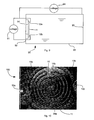
- an x-ray tube 90 is shown utilizing an electron emitter or filament device 94 , according to one of the embodiments described herein, including a planar filament 11 .
- the x-ray tube 90 can include a vacuum tube or vacuum enclosure 95 including opposing cathode 92 and anode 93 .
- the planar filament 11 can be adhered to the cathode 92 . Electrical connections can be made to the bonding pads 12 a and 12 b to allow an electrical current to flow through the planar filament 11 from a power source 91 .
- the planar filament 11 can be a large negative bias voltage compared to the anode 93 .
- the large negative bias voltage can be supplied by a high voltage power supply 94 .
- the electrical current in the planar filament 11 can heat the planar filament, resulting in electron emission from the planar filament 11 .
- the large bias voltage between the anode 93 and the planar filament 11 can result in an electron beam from the planar filament to the anode 93 .
- the electron spot on the anode 93 can be smaller and more circular than with helical filaments.
- a planar filament with a substrate 52 or support structure can be more easily placed in the same location in each x-ray tube that is manufactured, resulting in less manufacturing variation.
- Various aspects of x-ray tubes are shown and described in U.S. Pat. No. 7,382,862; and U.S. patent application Ser. No. 11/879,970, filed Jul. 18, 2007; which are herein incorporated by reference.
- FIG. 10 shows a photograph of an electron emitter or filament device 100 including a planar filament 11 .
- the planar filament 11 includes central spiral shaped sections 14 a - b , a wider, intermediate section 15 , and outer, serpentine sections 18 a - b . It also includes bonding pads 12 a - b.
- bonding pads 12 can be smaller, and/or can be configured for any type of electrical connection to the power source.
- Bonding pads 12 can include a post, a pad, or any other device configured to allow for an electrical connection in order to allow an electrical current to flow through the planar filament 11 .
- the filament 11 , bond pads 12 a - b , and/or beam shaping pads can be a thin film material.
- the planar filament can be connected to a type of support structure.
- a support structure which electrically isolates one bond pad 12 a from the other bond pad 12 b can be used to allow an electrical current to flow from one bond pad to the other through the planar filament 11 .
- the support structure can be situated such that it does not touch the planar filament 11 . This may be desirable in order to avoid conductive heat transfer from the planar filament 11 to the support structure.
- electron emitter or filament device 110 in FIG. 11 can be supported by electrically isolated support structures 112 a and 112 b .
- An electrical connection can be made directly to the bond pads 12 a and 12 b , with a different electrical potential on one bond pad 12 a than on the other bond pad 12 b , thus allowing an electrical current to flow through the planar filament 11 .
- the support structures 112 a and 112 b are electrically conductive, an electrical connection can be made to the support structures, with a different electrical potential on one support structure 112 a than on the other support structure 112 b , thus allowing an electrical current to flow through the planar filament 11 .
- the support structures can be a shape that allows easy placement into the equipment where the planar filament will be used.
- the support structures 112 a - b can be attached to a support base 113 for additional structural strength and to aid in handling and placement of the planar filament 11 .
- This support base 113 can have high electrical resistance in order to electrically isolate one support structure 112 and thus also one bond pad 12 from the other.
- the support structures 112 can be mounted onto the support base 113 with an adhesive, by pushing the support structures 112 into holes in the support base 113 , with fasteners such as screws, or other appropriate fastening method.
- a laser can be used to cut the layer 24 to create the planar filament 11 and bond pad 12 shapes.
- the planar filament 11 and bond pad 12 shapes can be made by photolithography techniques.
- the layer 24 can be coated with photo-resist, exposed to create the desired pattern, then etched.
- These methods of making the planar filament 11 and bond pad 12 a and 12 b shapes apply to all embodiments of the filament device discussed in this application. These methods also apply to making the beam shaping pads.
- Forming the planar filament 11 and bond pad 12 structure through laser machining or forming the filament and bond pad structure through photolithography techniques may be referred to herein as “patterned” or “patterning”.
- the layer 24 can be laser or spot welded onto the support structures 112 a and 112 b .
- the support structures 112 a and 112 b can hold the layer 24 in place while cutting out the planar filament 11 and bond pads 12 a and 12 b as discussed previously.
- the bond pads 12 a and 12 b can be laser welded onto the support structures 22 a and 22 b after the bond pads 12 a and 12 b and filament 11 have been cut.
- the electron emitter or filament device 120 can be made by attaching, such as by brazing or laser welding, planar layer 24 onto a substrate 52 .
- the substrate 52 can be a heat resistive, electrically insulating material, such as alumina or silicon. The substrate 52 can aid in handling the planar filament without damage and placing it consistently in the desired equipment location.
- a space 53 can be disposed between the planar filament 11 and the substrate 52 such that a substantial portion of the filament, such as all or a majority of the planar filament 11 , is suspended above the substrate 52 by the pair of boding pads 12 .
- the space 53 beneath the planar filament 11 can be an open area such as a vacuum, air, or other gas.
- the substrate 52 can be wholly or partially removed beneath the filament forming a recess or cavity 53 b bounded by the substrate on the sides (and possibly the bottom) with the planar filament 11 on top.
- High filament temperatures are normally needed for electron emission in an x-ray tube. To avoid conductive heat transfer away from the planar filament, it can be beneficial to remove the substrate 52 beneath most or all of the filament area.
- a layer 24 can be brazed onto a substrate 52 .
- a cavity or hole 53 b can be cut in the substrate 52 .
- the bond pad 12 and planar filament 11 shapes can be cut out by laser machining or patterning and etching as described previously.
Abstract
Description
-
- As used herein, the term “substantially” refers to the complete or nearly complete extent or degree of an action, characteristic, property, state, structure, item, or result. For example, an object that is “substantially” enclosed would mean that the object is either completely enclosed or nearly completely enclosed. The exact allowable degree of deviation from absolute completeness may in some cases depend on the specific context. However, generally speaking the nearness of completion will be so as to have the same overall result as if absolute and total completion were obtained. The use of “substantially” is equally applicable when used in a negative connotation to refer to the complete or near complete lack of an action, characteristic, property, state, structure, item, or result.
Claims (20)
Priority Applications (1)
| Application Number | Priority Date | Filing Date | Title |
|---|---|---|---|
| US13/209,862 US8247971B1 (en) | 2009-03-19 | 2011-08-15 | Resistively heated small planar filament |
Applications Claiming Priority (2)
| Application Number | Priority Date | Filing Date | Title |
|---|---|---|---|
| US12/407,457 US20100239828A1 (en) | 2009-03-19 | 2009-03-19 | Resistively heated small planar filament |
| US13/209,862 US8247971B1 (en) | 2009-03-19 | 2011-08-15 | Resistively heated small planar filament |
Related Parent Applications (1)
| Application Number | Title | Priority Date | Filing Date |
|---|---|---|---|
| US12/407,457 Continuation-In-Part US20100239828A1 (en) | 2009-03-19 | 2009-03-19 | Resistively heated small planar filament |
Publications (2)
| Publication Number | Publication Date |
|---|---|
| US8247971B1 true US8247971B1 (en) | 2012-08-21 |
| US20120212157A1 US20120212157A1 (en) | 2012-08-23 |
Family
ID=46641587
Family Applications (1)
| Application Number | Title | Priority Date | Filing Date |
|---|---|---|---|
| US13/209,862 Expired - Fee Related US8247971B1 (en) | 2009-03-19 | 2011-08-15 | Resistively heated small planar filament |
Country Status (1)
| Country | Link |
|---|---|
| US (1) | US8247971B1 (en) |
Cited By (9)
| Publication number | Priority date | Publication date | Assignee | Title |
|---|---|---|---|---|
| US20140153698A1 (en) * | 2012-12-05 | 2014-06-05 | Shimadzu Corporation | Flat filament for an x-ray tube, and an x-ray tube |
| US9072154B2 (en) | 2012-12-21 | 2015-06-30 | Moxtek, Inc. | Grid voltage generation for x-ray tube |
| US20150262782A1 (en) * | 2012-09-12 | 2015-09-17 | Shimadzu Corporation | X-ray tube device and method for using x-ray tube device |
| US9177755B2 (en) | 2013-03-04 | 2015-11-03 | Moxtek, Inc. | Multi-target X-ray tube with stationary electron beam position |
| US9184020B2 (en) | 2013-03-04 | 2015-11-10 | Moxtek, Inc. | Tiltable or deflectable anode x-ray tube |
| US20170092456A1 (en) * | 2015-09-28 | 2017-03-30 | General Electric Company | Flexible flat emitter for x-ray tubes |
| US20170287670A1 (en) * | 2016-04-01 | 2017-10-05 | Toshiba Electron Tubes & Devices Co., Ltd. | Emitter and x-ray tube |
| US20180350549A1 (en) * | 2017-06-05 | 2018-12-06 | General Electric Company | Flat Emitters With Stress Compensation Features |
| US11728120B2 (en) | 2021-02-10 | 2023-08-15 | Moxtek, Inc. | Planar filament with directed electron beam |
Families Citing this family (2)
| Publication number | Priority date | Publication date | Assignee | Title |
|---|---|---|---|---|
| WO2015066246A1 (en) | 2013-10-29 | 2015-05-07 | Varian Medical Systems, Inc. | X-ray tube having planar emitter with tunable emission characteristics and magnetic steering and focusing |
| RU179629U1 (en) * | 2018-01-16 | 2018-05-21 | Федеральное государственное унитарное предприятие "Научно-исследовательский институт Научно-производственное объединение "ЛУЧ" (ФГУП "НИИ НПО "ЛУЧ") | MINIATURE SOURCE OF X-RAY RADIATION |
Citations (251)
| Publication number | Priority date | Publication date | Assignee | Title |
|---|---|---|---|---|
| US1276706A (en) | 1918-04-30 | 1918-08-27 | Gurdy L Aydelotte | Land-torpedo. |
| US1881448A (en) | 1928-08-15 | 1932-10-11 | Formell Corp Ltd | X-ray method and means |
| US1946288A (en) | 1929-09-19 | 1934-02-06 | Gen Electric | Electron discharge device |
| US2291948A (en) | 1940-06-27 | 1942-08-04 | Westinghouse Electric & Mfg Co | High voltage X-ray tube shield |
| US2316214A (en) | 1940-09-10 | 1943-04-13 | Gen Electric X Ray Corp | Control of electron flow |
| US2329318A (en) | 1941-09-08 | 1943-09-14 | Gen Electric X Ray Corp | X-ray generator |
| US2340363A (en) | 1942-03-03 | 1944-02-01 | Gen Electric X Ray Corp | Control for focal spot in X-ray generators |
| US2502070A (en) | 1949-01-19 | 1950-03-28 | Dunlee Corp | Getter for induction flashing |
| US2663812A (en) | 1950-03-04 | 1953-12-22 | Philips Lab Inc | X-ray tube window |
| US2683223A (en) | 1952-07-24 | 1954-07-06 | Licentia Gmbh | X-ray tube |
| DE1030936B (en) | 1952-01-11 | 1958-05-29 | Licentia Gmbh | Vacuum-tight radiation window made of beryllium for discharge vessels |
| US2952790A (en) | 1957-07-15 | 1960-09-13 | Raytheon Co | X-ray tubes |
| US3218559A (en) | 1961-11-09 | 1965-11-16 | Gen Electric | Synchronizing circuit maintaining loop signals as an integer product and equal amplitude |
| US3356559A (en) | 1963-07-01 | 1967-12-05 | University Patents Inc | Colored fiber metal structures and method of making the same |
| US3358368A (en) | 1966-03-08 | 1967-12-19 | Eversharp Inc | Adjustable double edge razor |
| US3397337A (en) | 1966-01-14 | 1968-08-13 | Ion Physics Corp | Flash X-ray dielectric wall structure |
| US3434062A (en) | 1965-06-21 | 1969-03-18 | James R Cox | Drift detector |
| GB1252290A (en) | 1967-12-28 | 1971-11-03 | ||
| US3665236A (en) | 1970-12-09 | 1972-05-23 | Atomic Energy Commission | Electrode structure for controlling electron flow with high transmission efficiency |
| US3679927A (en) | 1970-08-17 | 1972-07-25 | Machlett Lab Inc | High power x-ray tube |
| US3691417A (en) | 1969-09-02 | 1972-09-12 | Watkins Johnson Co | X-ray generating assembly and system |
| US3741797A (en) | 1970-04-30 | 1973-06-26 | Gen Technology Corp | Low density high-strength boron on beryllium reinforcement filaments |
| US3751701A (en) | 1971-03-08 | 1973-08-07 | Watkins Johnson Co | Convergent flow hollow beam x-ray gun with high average power |
| US3801847A (en) | 1971-11-04 | 1974-04-02 | Siemens Ag | X-ray tube |
| US3828190A (en) | 1969-01-17 | 1974-08-06 | Measurex Corp | Detector assembly |
| US3851266A (en) | 1967-07-27 | 1974-11-26 | P Conway | Signal conditioner and bit synchronizer |
| US3872287A (en) | 1971-07-30 | 1975-03-18 | Philips Corp | Method of, and apparatus for, determining radiation energy distributions |
| US3882339A (en) | 1974-06-17 | 1975-05-06 | Gen Electric | Gridded X-ray tube gun |
| US3894219A (en) | 1974-01-16 | 1975-07-08 | Westinghouse Electric Corp | Hybrid analog and digital comb filter for clutter cancellation |
| US3962583A (en) | 1974-12-30 | 1976-06-08 | The Machlett Laboratories, Incorporated | X-ray tube focusing means |
| US3970884A (en) | 1973-07-09 | 1976-07-20 | Golden John P | Portable X-ray device |
| US4007375A (en) | 1975-07-14 | 1977-02-08 | Albert Richard D | Multi-target X-ray source |
| US4075526A (en) | 1975-11-28 | 1978-02-21 | Compagnie Generale De Radiologie | Hot-cathode x-ray tube having an end-mounted anode |
| US4160311A (en) | 1976-01-16 | 1979-07-10 | U.S. Philips Corporation | Method of manufacturing a cathode ray tube for displaying colored pictures |
| US4163900A (en) | 1977-08-17 | 1979-08-07 | Connecticut Research Institute, Inc. | Composite electron microscope grid suitable for energy dispersive X-ray analysis, process for producing the same and other micro-components |
| US4178509A (en) | 1978-06-02 | 1979-12-11 | The Bendix Corporation | Sensitivity proportional counter window |
| US4184097A (en) | 1977-02-25 | 1980-01-15 | Magnaflux Corporation | Internally shielded X-ray tube |
| US4250127A (en) | 1977-08-17 | 1981-02-10 | Connecticut Research Institute, Inc. | Production of electron microscope grids and other micro-components |
| US4293373A (en) | 1978-05-30 | 1981-10-06 | International Standard Electric Corporation | Method of making transducer |
| US4368538A (en) | 1980-04-11 | 1983-01-11 | International Business Machines Corporation | Spot focus flash X-ray source |
| US4393127A (en) | 1980-09-19 | 1983-07-12 | International Business Machines Corporation | Structure with a silicon body having through openings |
| US4421986A (en) | 1980-11-21 | 1983-12-20 | The United States Of America As Represented By The Department Of Health And Human Services | Nuclear pulse discriminator |
| US4443293A (en) | 1981-04-20 | 1984-04-17 | Kulite Semiconductor Products, Inc. | Method of fabricating transducer structure employing vertically walled diaphragms with quasi rectangular active areas |
| US4463338A (en) | 1980-08-28 | 1984-07-31 | Siemens Aktiengesellschaft | Electrical network and method for producing the same |
| US4504895A (en) | 1982-11-03 | 1985-03-12 | General Electric Company | Regulated dc-dc converter using a resonating transformer |
| US4521902A (en) | 1983-07-05 | 1985-06-04 | Ridge, Inc. | Microfocus X-ray system |
| US4532150A (en) | 1982-12-29 | 1985-07-30 | Shin-Etsu Chemical Co., Ltd. | Method for providing a coating layer of silicon carbide on the surface of a substrate |
| US4573186A (en) | 1982-06-16 | 1986-02-25 | Feinfocus Rontgensysteme Gmbh | Fine focus X-ray tube and method of forming a microfocus of the electron emission of an X-ray tube hot cathode |
| US4576679A (en) | 1981-03-27 | 1986-03-18 | Honeywell Inc. | Method of fabricating a cold shield |
| US4584056A (en) | 1983-11-18 | 1986-04-22 | Centre Electronique Horloger S.A. | Method of manufacturing a device with micro-shutters and application of such a method to obtain a light modulating device |
| US4591756A (en) | 1985-02-25 | 1986-05-27 | Energy Sciences, Inc. | High power window and support structure for electron beam processors |
| US4608326A (en) | 1984-02-13 | 1986-08-26 | Hewlett-Packard Company | Silicon carbide film for X-ray masks and vacuum windows |
| US4645977A (en) | 1984-08-31 | 1987-02-24 | Matsushita Electric Industrial Co., Ltd. | Plasma CVD apparatus and method for forming a diamond like carbon film |
| US4675525A (en) | 1985-02-06 | 1987-06-23 | Commissariat A L'energie Atomique | Matrix device for the detection of light radiation with individual cold screens integrated into a substrate and its production process |
| US4679219A (en) | 1984-06-15 | 1987-07-07 | Kabushiki Kaisha Toshiba | X-ray tube |
| US4688241A (en) | 1984-03-26 | 1987-08-18 | Ridge, Inc. | Microfocus X-ray system |
| US4696994A (en) | 1984-12-14 | 1987-09-29 | Ube Industries, Ltd. | Transparent aromatic polyimide |
| US4705540A (en) | 1986-04-17 | 1987-11-10 | E. I. Du Pont De Nemours And Company | Polyimide gas separation membranes |
| US4777642A (en) | 1985-07-24 | 1988-10-11 | Kabushiki Kaisha Toshiba | X-ray tube device |
| US4797907A (en) | 1987-08-07 | 1989-01-10 | Diasonics Inc. | Battery enhanced power generation for mobile X-ray machine |
| US4818806A (en) | 1985-05-31 | 1989-04-04 | Chisso Corporation | Process for producing highly adherent silicon-containing polyamic acid and corsslinked silicon-containing polyimide |
| US4819260A (en) | 1985-11-28 | 1989-04-04 | Siemens Aktiengesellschaft | X-radiator with non-migrating focal spot |
| US4862490A (en) | 1986-10-23 | 1989-08-29 | Hewlett-Packard Company | Vacuum windows for soft x-ray machines |
| US4870671A (en) | 1988-10-25 | 1989-09-26 | X-Ray Technologies, Inc. | Multitarget x-ray tube |
| US4876330A (en) | 1985-03-10 | 1989-10-24 | Nitto Electric Industrial Co., Ltd. | Colorless transparent polyimide shaped article and process for producing the same |
| US4878866A (en) | 1986-07-14 | 1989-11-07 | Denki Kagaku Kogyo Kabushiki Kaisha | Thermionic cathode structure |
| US4885055A (en) | 1987-08-21 | 1989-12-05 | Brigham Young University | Layered devices having surface curvature and method of constructing same |
| US4891831A (en) | 1987-07-24 | 1990-01-02 | Hitachi, Ltd. | X-ray tube and method for generating X-rays in the X-ray tube |
| US4933557A (en) | 1988-06-06 | 1990-06-12 | Brigham Young University | Radiation detector window structure and method of manufacturing thereof |
| US4939763A (en) | 1988-10-03 | 1990-07-03 | Crystallume | Method for preparing diamond X-ray transmissive elements |
| US4957773A (en) | 1989-02-13 | 1990-09-18 | Syracuse University | Deposition of boron-containing films from decaborane |
| US4960486A (en) | 1988-06-06 | 1990-10-02 | Brigham Young University | Method of manufacturing radiation detector window structure |
| US4969173A (en) | 1986-12-23 | 1990-11-06 | U.S. Philips Corporation | X-ray tube comprising an annular focus |
| EP0400655A1 (en) | 1989-06-01 | 1990-12-05 | Seiko Instruments Inc. | Optical window piece |
| US4979198A (en) | 1986-05-15 | 1990-12-18 | Malcolm David H | Method for production of fluoroscopic and radiographic x-ray images and hand held diagnostic apparatus incorporating the same |
| US4979199A (en) | 1989-10-31 | 1990-12-18 | General Electric Company | Microfocus X-ray tube with optical spot size sensing means |
| US5010562A (en) | 1989-08-31 | 1991-04-23 | Siemens Medical Laboratories, Inc. | Apparatus and method for inhibiting the generation of excessive radiation |
| US5063324A (en) | 1990-03-29 | 1991-11-05 | Itt Corporation | Dispenser cathode with emitting surface parallel to ion flow |
| US5066300A (en) | 1988-05-02 | 1991-11-19 | Nu-Tech Industries, Inc. | Twin replacement heart |
| EP0297808B1 (en) | 1987-07-02 | 1991-12-11 | MITSUI TOATSU CHEMICALS, Inc. | Polyimide and high-temperature adhesive thereof |
| US5077771A (en) | 1989-03-01 | 1991-12-31 | Kevex X-Ray Inc. | Hand held high power pulsed precision x-ray source |
| US5077777A (en) | 1990-07-02 | 1991-12-31 | Micro Focus Imaging Corp. | Microfocus X-ray tube |
| US5090046A (en) | 1988-11-30 | 1992-02-18 | Outokumpu Oy | Analyzer detector window and a method for manufacturing the same |
| US5105456A (en) | 1988-11-23 | 1992-04-14 | Imatron, Inc. | High duty-cycle x-ray tube |
| US5117829A (en) | 1989-03-31 | 1992-06-02 | Loma Linda University Medical Center | Patient alignment system and procedure for radiation treatment |
| US5153900A (en) | 1990-09-05 | 1992-10-06 | Photoelectron Corporation | Miniaturized low power x-ray source |
| US5161179A (en) | 1990-03-01 | 1992-11-03 | Yamaha Corporation | Beryllium window incorporated in X-ray radiation system and process of fabrication thereof |
| US5173612A (en) | 1990-09-18 | 1992-12-22 | Sumitomo Electric Industries Ltd. | X-ray window and method of producing same |
| US5178140A (en) | 1991-09-05 | 1993-01-12 | Telectronics Pacing Systems, Inc. | Implantable medical devices employing capacitive control of high voltage switches |
| US5196283A (en) | 1989-03-09 | 1993-03-23 | Canon Kabushiki Kaisha | X-ray mask structure, and x-ray exposure process |
| US5217817A (en) | 1989-11-08 | 1993-06-08 | U.S. Philips Corporation | Steel tool provided with a boron layer |
| US5226067A (en) | 1992-03-06 | 1993-07-06 | Brigham Young University | Coating for preventing corrosion to beryllium x-ray windows and method of preparing |
| USRE34421E (en) | 1990-11-21 | 1993-10-26 | Parker William J | X-ray micro-tube and method of use in radiation oncology |
| US5258091A (en) | 1990-09-18 | 1993-11-02 | Sumitomo Electric Industries, Ltd. | Method of producing X-ray window |
| US5267294A (en) | 1992-04-22 | 1993-11-30 | Hitachi Medical Corporation | Radiotherapy apparatus |
| US5302523A (en) | 1989-06-21 | 1994-04-12 | Zeneca Limited | Transformation of plant cells |
| US5343112A (en) | 1989-01-18 | 1994-08-30 | Balzers Aktiengesellschaft | Cathode arrangement |
| EP0330456B1 (en) | 1988-02-26 | 1994-09-07 | Chisso Corporation | Preparation of silicon-containing polyimide precursor and cured polyimides obtained therefrom |
| US5392042A (en) | 1993-08-05 | 1995-02-21 | Martin Marietta Corporation | Sigma-delta analog-to-digital converter with filtration having controlled pole-zero locations, and apparatus therefor |
| US5391958A (en) | 1993-04-12 | 1995-02-21 | Charged Injection Corporation | Electron beam window devices and methods of making same |
| US5400385A (en) | 1993-09-02 | 1995-03-21 | General Electric Company | High voltage power supply for an X-ray tube |
| US5422926A (en) | 1990-09-05 | 1995-06-06 | Photoelectron Corporation | X-ray source with shaped radiation pattern |
| US5432003A (en) | 1988-10-03 | 1995-07-11 | Crystallume | Continuous thin diamond film and method for making same |
| US5469429A (en) | 1993-05-21 | 1995-11-21 | Kabushiki Kaisha Toshiba | X-ray CT apparatus having focal spot position detection means for the X-ray tube and focal spot position adjusting means |
| US5469490A (en) | 1993-10-26 | 1995-11-21 | Golden; John | Cold-cathode X-ray emitter and tube therefor |
| US5478266A (en) | 1993-04-12 | 1995-12-26 | Charged Injection Corporation | Beam window devices and methods of making same |
| US5521851A (en) | 1993-04-26 | 1996-05-28 | Nihon Kohden Corporation | Noise reduction method and apparatus |
| US5524133A (en) | 1992-01-15 | 1996-06-04 | Cambridge Imaging Limited | Material identification using x-rays |
| US5571616A (en) | 1995-05-16 | 1996-11-05 | Crystallume | Ultrasmooth adherent diamond film coated article and method for making same |
| USRE35383E (en) | 1992-03-23 | 1996-11-26 | The Titan Corporation | Interstitial X-ray needle |
| US5578360A (en) | 1992-05-07 | 1996-11-26 | Outokumpu Instruments Oy | Thin film reinforcing structure and method for manufacturing the same |
| US5602507A (en) | 1993-11-05 | 1997-02-11 | Ntt Mobile Communications Network Inc. | Adaptive demodulating method for generating replica and demodulator thereof |
| US5607723A (en) | 1988-10-21 | 1997-03-04 | Crystallume | Method for making continuous thin diamond film |
| US5621780A (en) | 1990-09-05 | 1997-04-15 | Photoelectron Corporation | X-ray apparatus for applying a predetermined flux to an interior surface of a body cavity |
| US5627871A (en) | 1993-06-10 | 1997-05-06 | Nanodynamics, Inc. | X-ray tube and microelectronics alignment process |
| US5631943A (en) | 1995-12-19 | 1997-05-20 | Miles; Dale A. | Portable X-ray device |
| US5673044A (en) | 1995-08-24 | 1997-09-30 | Lockheed Martin Corporation | Cascaded recursive transversal filter for sigma-delta modulators |
| US5680433A (en) | 1995-04-28 | 1997-10-21 | Varian Associates, Inc. | High output stationary X-ray target with flexible support structure |
| US5682412A (en) | 1993-04-05 | 1997-10-28 | Cardiac Mariners, Incorporated | X-ray source |
| EP0676772B1 (en) | 1994-04-09 | 1997-10-29 | AEA Technology plc | Method of manufacturing of X-ray windows |
| US5696808A (en) | 1995-09-28 | 1997-12-09 | Siemens Aktiengesellschaft | X-ray tube |
| US5706354A (en) | 1995-07-10 | 1998-01-06 | Stroehlein; Brian A. | AC line-correlated noise-canceling circuit |
| US5729583A (en) | 1995-09-29 | 1998-03-17 | The United States Of America As Represented By The Secretary Of Commerce | Miniature x-ray source |
| US5774522A (en) | 1995-08-14 | 1998-06-30 | Warburton; William K. | Method and apparatus for digitally based high speed x-ray spectrometer for direct coupled use with continuous discharge preamplifiers |
| DE4430623C2 (en) | 1994-08-29 | 1998-07-02 | Siemens Ag | X-ray image intensifier |
| US5812632A (en) | 1996-09-27 | 1998-09-22 | Siemens Aktiengesellschaft | X-ray tube with variable focus |
| US5835561A (en) | 1993-01-25 | 1998-11-10 | Cardiac Mariners, Incorporated | Scanning beam x-ray imaging system |
| US5870051A (en) | 1995-08-14 | 1999-02-09 | William K. Warburton | Method and apparatus for analog signal conditioner for high speed, digital x-ray spectrometer |
| US5898754A (en) | 1997-06-13 | 1999-04-27 | X-Ray And Specialty Instruments, Inc. | Method and apparatus for making a demountable x-ray tube |
| US5907595A (en) | 1997-08-18 | 1999-05-25 | General Electric Company | Emitter-cup cathode for high-emission x-ray tube |
| DE19818057A1 (en) | 1998-04-22 | 1999-11-04 | Siemens Ag | X-ray image intensifier manufacture method |
| US6002202A (en) | 1996-07-19 | 1999-12-14 | The Regents Of The University Of California | Rigid thin windows for vacuum applications |
| US6005918A (en) | 1997-12-19 | 1999-12-21 | Picker International, Inc. | X-ray tube window heat shield |
| US6044130A (en) | 1995-12-25 | 2000-03-28 | Hamamatsu Photonics K.K. | Transmission type X-ray tube |
| US6062931A (en) | 1999-09-01 | 2000-05-16 | Industrial Technology Research Institute | Carbon nanotube emitter with triode structure |
| US6063629A (en) | 1998-06-05 | 2000-05-16 | Wolfgang Lummel | Microinjection process for introducing an injection substance particularly foreign, genetic material, into procaryotic and eucaryotic cells, as well as cell compartments of the latter (plastids, cell nuclei), as well as nanopipette for the same |
| US6069278A (en) | 1998-01-23 | 2000-05-30 | The United States Of America As Represented By The Administrator Of The National Aeronautics And Space Administration | Aromatic diamines and polyimides based on 4,4'-bis-(4-aminophenoxy)-2,2' or 2,2',6,6'-substituted biphenyl |
| US6075839A (en) | 1997-09-02 | 2000-06-13 | Varian Medical Systems, Inc. | Air cooled end-window metal-ceramic X-ray tube for lower power XRF applications |
| US6073484A (en) | 1995-07-20 | 2000-06-13 | Cornell Research Foundation, Inc. | Microfabricated torsional cantilevers for sensitive force detection |
| US6097790A (en) | 1997-02-26 | 2000-08-01 | Canon Kabushiki Kaisha | Pressure partition for X-ray exposure apparatus |
| US6129901A (en) | 1997-11-18 | 2000-10-10 | Martin Moskovits | Controlled synthesis and metal-filling of aligned carbon nanotubes |
| US6134300A (en) | 1998-11-05 | 2000-10-17 | The Regents Of The University Of California | Miniature x-ray source |
| US6133401A (en) | 1998-06-29 | 2000-10-17 | The United States Of America As Represented By The Administrator Of The National Aeronautics And Space Administration | Method to prepare processable polyimides with reactive endgroups using 1,3-bis (3-aminophenoxy) benzene |
| US6184333B1 (en) | 1998-01-16 | 2001-02-06 | Maverick Corporation | Low-toxicity, high-temperature polyimides |
| US6205200B1 (en) | 1996-10-28 | 2001-03-20 | The United States Of America As Represented By The Secretary Of The Navy | Mobile X-ray unit |
| JP3170673B2 (en) | 1994-11-15 | 2001-05-28 | 株式会社テイエルブイ | Liquid pumping device |
| US6277318B1 (en) | 1999-08-18 | 2001-08-21 | Agere Systems Guardian Corp. | Method for fabrication of patterned carbon nanotube films |
| US6282263B1 (en) | 1996-09-27 | 2001-08-28 | Bede Scientific Instruments Limited | X-ray generator |
| US6307008B1 (en) | 2000-02-25 | 2001-10-23 | Saehan Industries Corporation | Polyimide for high temperature adhesive |
| US6320019B1 (en) | 2000-02-22 | 2001-11-20 | Saehan Industries Incorporation | Method for the preparation of polyamic acid and polyimide |
| US6351520B1 (en) | 1997-12-04 | 2002-02-26 | Hamamatsu Photonics K.K. | X-ray tube |
| US6385294B2 (en) | 1998-07-30 | 2002-05-07 | Hamamatsu Photonics K.K. | X-ray tube |
| US6388359B1 (en) | 2000-03-03 | 2002-05-14 | Optical Coating Laboratory, Inc. | Method of actuating MEMS switches |
| US20020075999A1 (en) | 2000-09-29 | 2002-06-20 | Peter Rother | Vacuum enclosure for a vacuum tube tube having an X-ray window |
| US20020094064A1 (en) | 2000-10-06 | 2002-07-18 | Zhou Otto Z. | Large-area individually addressable multi-beam x-ray system and method of forming same |
| US6438207B1 (en) | 1999-09-14 | 2002-08-20 | Varian Medical Systems, Inc. | X-ray tube having improved focal spot control |
| US6477235B2 (en) | 1999-03-23 | 2002-11-05 | Victor Ivan Chornenky | X-Ray device and deposition process for manufacture |
| US6487273B1 (en) | 1999-11-26 | 2002-11-26 | Varian Medical Systems, Inc. | X-ray tube having an integral housing assembly |
| US6487272B1 (en) | 1999-02-19 | 2002-11-26 | Kabushiki Kaisha Toshiba | Penetrating type X-ray tube and manufacturing method thereof |
| US6494618B1 (en) | 2000-08-15 | 2002-12-17 | Varian Medical Systems, Inc. | High voltage receptacle for x-ray tubes |
| JP2003007237A (en) | 2001-06-25 | 2003-01-10 | Shimadzu Corp | X-ray generator |
| JP2003510236A (en) | 1999-09-23 | 2003-03-18 | コモンウエルス サイエンティフィック アンド インダストリアル リサーチ オーガナイゼーション | Patterned carbon nanotubes |
| JP2003088383A (en) | 2001-09-19 | 2003-03-25 | Tokyo Inst Of Technol | Method for collecting biomolecule from live cell |
| US6546077B2 (en) | 2001-01-17 | 2003-04-08 | Medtronic Ave, Inc. | Miniature X-ray device and method of its manufacture |
| US20030096104A1 (en) | 2001-03-15 | 2003-05-22 | Polymatech Co., Ltd. | Carbon nanotube complex molded body and the method of making the same |
| US20030117770A1 (en) | 2001-12-20 | 2003-06-26 | Intel Corporation | Carbon nanotube thermal interface structures |
| JP2003211396A (en) | 2002-01-21 | 2003-07-29 | Ricoh Co Ltd | Micromachine |
| US20030152700A1 (en) | 2002-02-11 | 2003-08-14 | Board Of Trustees Operating Michigan State University | Process for synthesizing uniform nanocrystalline films |
| US20030165418A1 (en) | 2002-02-11 | 2003-09-04 | Rensselaer Polytechnic Institute | Directed assembly of highly-organized carbon nanotube architectures |
| US6646366B2 (en) | 2001-07-24 | 2003-11-11 | Siemens Aktiengesellschaft | Directly heated thermionic flat emitter |
| US6645757B1 (en) | 2001-02-08 | 2003-11-11 | Sandia Corporation | Apparatus and method for transforming living cells |
| US6658085B2 (en) | 2000-08-04 | 2003-12-02 | Siemens Aktiengesellschaft | Medical examination installation with an MR system and an X-ray system |
| US6661876B2 (en) | 2001-07-30 | 2003-12-09 | Moxtek, Inc. | Mobile miniature X-ray source |
| US20040076260A1 (en) | 2002-01-31 | 2004-04-22 | Charles Jr Harry K. | X-ray source and method for more efficiently producing selectable x-ray frequencies |
| US6740874B2 (en) | 2001-04-26 | 2004-05-25 | Bruker Saxonia Analytik Gmbh | Ion mobility spectrometer with mechanically stabilized vacuum-tight x-ray window |
| US6778633B1 (en) | 1999-03-26 | 2004-08-17 | Bede Scientific Instruments Limited | Method and apparatus for prolonging the life of an X-ray target |
| US6799075B1 (en) | 1995-08-24 | 2004-09-28 | Medtronic Ave, Inc. | X-ray catheter |
| US6803571B1 (en) | 2003-06-26 | 2004-10-12 | Kla-Tencor Technologies Corporation | Method and apparatus for dual-energy e-beam inspector |
| US6803570B1 (en) | 2003-07-11 | 2004-10-12 | Charles E. Bryson, III | Electron transmissive window usable with high pressure electron spectrometry |
| US6816573B2 (en) | 1999-03-02 | 2004-11-09 | Hamamatsu Photonics K.K. | X-ray generating apparatus, X-ray imaging apparatus, and X-ray inspection system |
| US6819741B2 (en) | 2003-03-03 | 2004-11-16 | Varian Medical Systems Inc. | Apparatus and method for shaping high voltage potentials on an insulator |
| US6838297B2 (en) | 1998-03-27 | 2005-01-04 | Canon Kabushiki Kaisha | Nanostructure, electron emitting device, carbon nanotube device, and method of producing the same |
| US20050018817A1 (en) | 2002-02-20 | 2005-01-27 | Oettinger Peter E. | Integrated X-ray source module |
| US6852365B2 (en) | 2001-03-26 | 2005-02-08 | Kumetrix, Inc. | Silicon penetration device with increased fracture toughness and method of fabrication |
| US6900580B2 (en) | 1998-11-12 | 2005-05-31 | The Board Of Trustees Of The Leland Stanford Junior University | Self-oriented bundles of carbon nanotubes and method of making same |
| US20050141669A1 (en) | 2003-01-10 | 2005-06-30 | Toshiba Electron Tube & Devices Co., Ltd | X-ray equipment |
| US20050207537A1 (en) | 2002-07-19 | 2005-09-22 | Masaaki Ukita | X-ray generating equipment |
| US6956706B2 (en) | 2000-04-03 | 2005-10-18 | John Robert Brandon | Composite diamond window |
| US6962782B1 (en) | 1999-02-08 | 2005-11-08 | Commissariat A L'energie Atomique | Method for producing addressed ligands matrixes on a support |
| US6976953B1 (en) | 2000-03-30 | 2005-12-20 | The Board Of Trustees Of The Leland Stanford Junior University | Maintaining the alignment of electric and magnetic fields in an x-ray tube operated in a magnetic field |
| US6987835B2 (en) | 2003-03-26 | 2006-01-17 | Xoft Microtube, Inc. | Miniature x-ray tube with micro cathode |
| US20060073682A1 (en) | 2004-10-04 | 2006-04-06 | International Business Machines Corporation | Low-k dielectric material based upon carbon nanotubes and methods of forming such low-k dielectric materials |
| US7035379B2 (en) | 2002-09-13 | 2006-04-25 | Moxtek, Inc. | Radiation window and method of manufacture |
| US20060098778A1 (en) | 2002-02-20 | 2006-05-11 | Oettinger Peter E | Integrated X-ray source module |
| US7046767B2 (en) | 2001-05-31 | 2006-05-16 | Hamamatsu Photonics K.K. | X-ray generator |
| US7049735B2 (en) | 2004-01-07 | 2006-05-23 | Matsushita Electric Industrial Co., Ltd. | Incandescent bulb and incandescent bulb filament |
| US7050539B2 (en) | 2001-12-06 | 2006-05-23 | Koninklijke Philips Electronics N.V. | Power supply for an X-ray generator |
| US7075699B2 (en) | 2003-09-29 | 2006-07-11 | The Regents Of The University Of California | Double hidden flexure microactuator for phase mirror array |
| US7085354B2 (en) | 2003-01-21 | 2006-08-01 | Toshiba Electron Tube & Devices Co., Ltd. | X-ray tube apparatus |
| US7108841B2 (en) | 1997-03-07 | 2006-09-19 | William Marsh Rice University | Method for forming a patterned array of single-wall carbon nanotubes |
| US7110498B2 (en) | 2003-09-12 | 2006-09-19 | Canon Kabushiki Kaisha | Image reading apparatus and X-ray imaging apparatus |
| US20060210020A1 (en) | 2003-05-15 | 2006-09-21 | Jun Takahashi | X-ray generation device |
| US20060233307A1 (en) | 2001-06-19 | 2006-10-19 | Mark Dinsmore | X-ray source for materials analysis systems |
| US7130381B2 (en) | 2004-03-13 | 2006-10-31 | Xoft, Inc. | Extractor cup on a miniature x-ray tube |
| JP2006297549A (en) | 2005-04-21 | 2006-11-02 | Keio Gijuku | Method for arranged vapor deposition of metal nanoparticle and method for growing carbon nanotube using metal nanoparticle |
| US20060269048A1 (en) | 2005-05-25 | 2006-11-30 | Cain Bruce A | Removable aperture cooling structure for an X-ray tube |
| US20060280289A1 (en) | 2005-06-08 | 2006-12-14 | Gary Hanington | X-ray tube driver using am and fm modulation |
| US20070025516A1 (en) | 2005-03-31 | 2007-02-01 | Bard Erik C | Magnetic head for X-ray source |
| US7203283B1 (en) | 2006-02-21 | 2007-04-10 | Oxford Instruments Analytical Oy | X-ray tube of the end window type, and an X-ray fluorescence analyzer |
| US20070087436A1 (en) | 2003-04-11 | 2007-04-19 | Atsushi Miyawaki | Microinjection method and device |
| US7215741B2 (en) | 2004-03-26 | 2007-05-08 | Shimadzu Corporation | X-ray generating apparatus |
| US20070111617A1 (en) | 2005-11-17 | 2007-05-17 | Oxford Instruments Analytical Oy | Window membrane for detector and analyser devices, and a method for manufacturing a window membrane |
| US7224769B2 (en) | 2004-02-20 | 2007-05-29 | Aribex, Inc. | Digital x-ray camera |
| US20070133921A1 (en) | 2005-12-08 | 2007-06-14 | Haffner Ken Y | Optical Sensor Device for Local Analysis of a Combustion Process in a Combustor of a Thermal Power Plant |
| US20070142781A1 (en) | 2005-12-21 | 2007-06-21 | Sayre Chauncey B | Microinjector chip |
| US20070165780A1 (en) | 2006-01-19 | 2007-07-19 | Bruker Axs, Inc. | Multiple wavelength X-ray source |
| US20070172104A1 (en) | 2006-01-19 | 2007-07-26 | Akihiko Nishide | Image display apparatus and x-ray ct apparatus |
| US20070176319A1 (en) | 2003-08-06 | 2007-08-02 | University Of Delaware | Aligned carbon nanotube composite ribbons and their production |
| US20070183576A1 (en) | 2006-01-31 | 2007-08-09 | Burke James E | Cathode head having filament protection features |
| US20070217574A1 (en) | 2006-03-15 | 2007-09-20 | Siemens Aktiengesellschaft | X-ray device |
| US7286642B2 (en) | 2002-04-05 | 2007-10-23 | Hamamatsu Photonics K.K. | X-ray tube control apparatus and x-ray tube control method |
| US7358593B2 (en) | 2004-05-07 | 2008-04-15 | University Of Maine | Microfabricated miniature grids |
| US7382862B2 (en) | 2005-09-30 | 2008-06-03 | Moxtek, Inc. | X-ray tube cathode with reduced unintended electrical field emission |
| US7399794B2 (en) | 2004-04-28 | 2008-07-15 | University Of South Florida | Polymer/carbon nanotube composites, methods of use and methods of synthesis thereof |
| US7410603B2 (en) | 2004-07-16 | 2008-08-12 | Nissin Kogyo Co., Ltd. | Carbon fiber-metal composite material and method of producing the same |
| US20080199399A1 (en) | 2007-02-21 | 2008-08-21 | Xing Chen | Interfacing Nanostructures to Biological Cells |
| JP4171700B2 (en) | 2001-11-21 | 2008-10-22 | ノバルティス アクチエンゲゼルシャフト | Heterocyclic compounds and methods of use |
| US20080296479A1 (en) | 2007-06-01 | 2008-12-04 | Anderson Eric C | Polymer X-Ray Window with Diamond Support Structure |
| US20080296518A1 (en) | 2007-06-01 | 2008-12-04 | Degao Xu | X-Ray Window with Grid Structure |
| US20080317982A1 (en) | 2006-10-13 | 2008-12-25 | Unidym, Inc. | Compliant and nonplanar nanostructure films |
| US20090086923A1 (en) | 2007-09-28 | 2009-04-02 | Davis Robert C | X-ray radiation window with carbon nanotube frame |
| US20090085426A1 (en) | 2007-09-28 | 2009-04-02 | Davis Robert C | Carbon nanotube mems assembly |
| US7529345B2 (en) | 2007-07-18 | 2009-05-05 | Moxtek, Inc. | Cathode header optic for x-ray tube |
| US20090213914A1 (en) | 2004-06-03 | 2009-08-27 | Silicon Laboratories Inc. | Capacitive isolation circuitry |
| US20090243028A1 (en) | 2004-06-03 | 2009-10-01 | Silicon Laboratories Inc. | Capacitive isolation circuitry with improved common mode detector |
| US7634052B2 (en) | 2006-10-24 | 2009-12-15 | Thermo Niton Analyzers Llc | Two-stage x-ray concentrator |
| US7649980B2 (en) | 2006-12-04 | 2010-01-19 | The University Of Tokyo | X-ray source |
| US7675444B1 (en) | 2008-09-23 | 2010-03-09 | Maxim Integrated Products, Inc. | High voltage isolation by capacitive coupling |
| US7680652B2 (en) | 2004-10-26 | 2010-03-16 | Qnx Software Systems (Wavemakers), Inc. | Periodic signal enhancement system |
| US7693265B2 (en) | 2006-05-11 | 2010-04-06 | Koninklijke Philips Electronics N.V. | Emitter design including emergency operation mode in case of emitter-damage for medical X-ray application |
| US20100098216A1 (en) | 2008-10-17 | 2010-04-22 | Moxtek, Inc. | Noise Reduction In Xray Emitter/Detector Systems |
| US20100096595A1 (en) | 2006-10-06 | 2010-04-22 | The Trustees Of Princeton University | Functional graphene-polymer nanocomposites for gas barrier applications |
| US7709820B2 (en) | 2007-06-01 | 2010-05-04 | Moxtek, Inc. | Radiation window with coated silicon support structure |
| US20100126660A1 (en) | 2008-10-30 | 2010-05-27 | O'hara David | Method of making graphene sheets and applicatios thereor |
| US20100140497A1 (en) | 2007-03-02 | 2010-06-10 | Protochips, Inc. | Membrane supports with reinforcement features |
| US20100189225A1 (en) | 2009-01-28 | 2010-07-29 | Phillippe Ernest | X-ray tube electrical power supply, associated power supply process and imaging system |
| US20100239828A1 (en) | 2009-03-19 | 2010-09-23 | Cornaby Sterling W | Resistively heated small planar filament |
| US20100248343A1 (en) | 2007-07-09 | 2010-09-30 | Aten Quentin T | Methods and Devices for Charged Molecule Manipulation |
| US20110017921A1 (en) | 2009-07-24 | 2011-01-27 | Tsinghua University | Carbon nanotube film composite structure, transmission electron microscope grid using the same, and method for making the same |
| US20110121179A1 (en) | 2007-06-01 | 2011-05-26 | Liddiard Steven D | X-ray window with beryllium support structure |
| US7983394B2 (en) | 2009-12-17 | 2011-07-19 | Moxtek, Inc. | Multiple wavelength X-ray source |
-
2011
- 2011-08-15 US US13/209,862 patent/US8247971B1/en not_active Expired - Fee Related
Patent Citations (276)
| Publication number | Priority date | Publication date | Assignee | Title |
|---|---|---|---|---|
| US1276706A (en) | 1918-04-30 | 1918-08-27 | Gurdy L Aydelotte | Land-torpedo. |
| US1881448A (en) | 1928-08-15 | 1932-10-11 | Formell Corp Ltd | X-ray method and means |
| US1946288A (en) | 1929-09-19 | 1934-02-06 | Gen Electric | Electron discharge device |
| US2291948A (en) | 1940-06-27 | 1942-08-04 | Westinghouse Electric & Mfg Co | High voltage X-ray tube shield |
| US2316214A (en) | 1940-09-10 | 1943-04-13 | Gen Electric X Ray Corp | Control of electron flow |
| US2329318A (en) | 1941-09-08 | 1943-09-14 | Gen Electric X Ray Corp | X-ray generator |
| US2340363A (en) | 1942-03-03 | 1944-02-01 | Gen Electric X Ray Corp | Control for focal spot in X-ray generators |
| US2502070A (en) | 1949-01-19 | 1950-03-28 | Dunlee Corp | Getter for induction flashing |
| US2663812A (en) | 1950-03-04 | 1953-12-22 | Philips Lab Inc | X-ray tube window |
| DE1030936B (en) | 1952-01-11 | 1958-05-29 | Licentia Gmbh | Vacuum-tight radiation window made of beryllium for discharge vessels |
| US2683223A (en) | 1952-07-24 | 1954-07-06 | Licentia Gmbh | X-ray tube |
| US2952790A (en) | 1957-07-15 | 1960-09-13 | Raytheon Co | X-ray tubes |
| US3218559A (en) | 1961-11-09 | 1965-11-16 | Gen Electric | Synchronizing circuit maintaining loop signals as an integer product and equal amplitude |
| US3356559A (en) | 1963-07-01 | 1967-12-05 | University Patents Inc | Colored fiber metal structures and method of making the same |
| US3434062A (en) | 1965-06-21 | 1969-03-18 | James R Cox | Drift detector |
| US3397337A (en) | 1966-01-14 | 1968-08-13 | Ion Physics Corp | Flash X-ray dielectric wall structure |
| US3358368A (en) | 1966-03-08 | 1967-12-19 | Eversharp Inc | Adjustable double edge razor |
| US3851266A (en) | 1967-07-27 | 1974-11-26 | P Conway | Signal conditioner and bit synchronizer |
| GB1252290A (en) | 1967-12-28 | 1971-11-03 | ||
| US3828190A (en) | 1969-01-17 | 1974-08-06 | Measurex Corp | Detector assembly |
| US3691417A (en) | 1969-09-02 | 1972-09-12 | Watkins Johnson Co | X-ray generating assembly and system |
| US3741797A (en) | 1970-04-30 | 1973-06-26 | Gen Technology Corp | Low density high-strength boron on beryllium reinforcement filaments |
| US3679927A (en) | 1970-08-17 | 1972-07-25 | Machlett Lab Inc | High power x-ray tube |
| US3665236A (en) | 1970-12-09 | 1972-05-23 | Atomic Energy Commission | Electrode structure for controlling electron flow with high transmission efficiency |
| US3751701A (en) | 1971-03-08 | 1973-08-07 | Watkins Johnson Co | Convergent flow hollow beam x-ray gun with high average power |
| US3872287A (en) | 1971-07-30 | 1975-03-18 | Philips Corp | Method of, and apparatus for, determining radiation energy distributions |
| US3801847A (en) | 1971-11-04 | 1974-04-02 | Siemens Ag | X-ray tube |
| US3970884A (en) | 1973-07-09 | 1976-07-20 | Golden John P | Portable X-ray device |
| US3894219A (en) | 1974-01-16 | 1975-07-08 | Westinghouse Electric Corp | Hybrid analog and digital comb filter for clutter cancellation |
| US3882339A (en) | 1974-06-17 | 1975-05-06 | Gen Electric | Gridded X-ray tube gun |
| US3962583A (en) | 1974-12-30 | 1976-06-08 | The Machlett Laboratories, Incorporated | X-ray tube focusing means |
| US4007375A (en) | 1975-07-14 | 1977-02-08 | Albert Richard D | Multi-target X-ray source |
| US4075526A (en) | 1975-11-28 | 1978-02-21 | Compagnie Generale De Radiologie | Hot-cathode x-ray tube having an end-mounted anode |
| US4160311A (en) | 1976-01-16 | 1979-07-10 | U.S. Philips Corporation | Method of manufacturing a cathode ray tube for displaying colored pictures |
| US4184097A (en) | 1977-02-25 | 1980-01-15 | Magnaflux Corporation | Internally shielded X-ray tube |
| US4250127A (en) | 1977-08-17 | 1981-02-10 | Connecticut Research Institute, Inc. | Production of electron microscope grids and other micro-components |
| US4163900A (en) | 1977-08-17 | 1979-08-07 | Connecticut Research Institute, Inc. | Composite electron microscope grid suitable for energy dispersive X-ray analysis, process for producing the same and other micro-components |
| US4293373A (en) | 1978-05-30 | 1981-10-06 | International Standard Electric Corporation | Method of making transducer |
| US4178509A (en) | 1978-06-02 | 1979-12-11 | The Bendix Corporation | Sensitivity proportional counter window |
| US4368538A (en) | 1980-04-11 | 1983-01-11 | International Business Machines Corporation | Spot focus flash X-ray source |
| US4463338A (en) | 1980-08-28 | 1984-07-31 | Siemens Aktiengesellschaft | Electrical network and method for producing the same |
| US4393127A (en) | 1980-09-19 | 1983-07-12 | International Business Machines Corporation | Structure with a silicon body having through openings |
| US4421986A (en) | 1980-11-21 | 1983-12-20 | The United States Of America As Represented By The Department Of Health And Human Services | Nuclear pulse discriminator |
| US4576679A (en) | 1981-03-27 | 1986-03-18 | Honeywell Inc. | Method of fabricating a cold shield |
| US4443293A (en) | 1981-04-20 | 1984-04-17 | Kulite Semiconductor Products, Inc. | Method of fabricating transducer structure employing vertically walled diaphragms with quasi rectangular active areas |
| US4573186A (en) | 1982-06-16 | 1986-02-25 | Feinfocus Rontgensysteme Gmbh | Fine focus X-ray tube and method of forming a microfocus of the electron emission of an X-ray tube hot cathode |
| US4504895A (en) | 1982-11-03 | 1985-03-12 | General Electric Company | Regulated dc-dc converter using a resonating transformer |
| US4532150A (en) | 1982-12-29 | 1985-07-30 | Shin-Etsu Chemical Co., Ltd. | Method for providing a coating layer of silicon carbide on the surface of a substrate |
| US4521902A (en) | 1983-07-05 | 1985-06-04 | Ridge, Inc. | Microfocus X-ray system |
| US4584056A (en) | 1983-11-18 | 1986-04-22 | Centre Electronique Horloger S.A. | Method of manufacturing a device with micro-shutters and application of such a method to obtain a light modulating device |
| US4608326A (en) | 1984-02-13 | 1986-08-26 | Hewlett-Packard Company | Silicon carbide film for X-ray masks and vacuum windows |
| US4688241A (en) | 1984-03-26 | 1987-08-18 | Ridge, Inc. | Microfocus X-ray system |
| US4679219A (en) | 1984-06-15 | 1987-07-07 | Kabushiki Kaisha Toshiba | X-ray tube |
| US4645977A (en) | 1984-08-31 | 1987-02-24 | Matsushita Electric Industrial Co., Ltd. | Plasma CVD apparatus and method for forming a diamond like carbon film |
| US4696994A (en) | 1984-12-14 | 1987-09-29 | Ube Industries, Ltd. | Transparent aromatic polyimide |
| US4675525A (en) | 1985-02-06 | 1987-06-23 | Commissariat A L'energie Atomique | Matrix device for the detection of light radiation with individual cold screens integrated into a substrate and its production process |
| US4591756A (en) | 1985-02-25 | 1986-05-27 | Energy Sciences, Inc. | High power window and support structure for electron beam processors |
| US4876330A (en) | 1985-03-10 | 1989-10-24 | Nitto Electric Industrial Co., Ltd. | Colorless transparent polyimide shaped article and process for producing the same |
| US4818806A (en) | 1985-05-31 | 1989-04-04 | Chisso Corporation | Process for producing highly adherent silicon-containing polyamic acid and corsslinked silicon-containing polyimide |
| US4777642A (en) | 1985-07-24 | 1988-10-11 | Kabushiki Kaisha Toshiba | X-ray tube device |
| US4819260A (en) | 1985-11-28 | 1989-04-04 | Siemens Aktiengesellschaft | X-radiator with non-migrating focal spot |
| US4705540A (en) | 1986-04-17 | 1987-11-10 | E. I. Du Pont De Nemours And Company | Polyimide gas separation membranes |
| US4979198A (en) | 1986-05-15 | 1990-12-18 | Malcolm David H | Method for production of fluoroscopic and radiographic x-ray images and hand held diagnostic apparatus incorporating the same |
| US4878866A (en) | 1986-07-14 | 1989-11-07 | Denki Kagaku Kogyo Kabushiki Kaisha | Thermionic cathode structure |
| US4862490A (en) | 1986-10-23 | 1989-08-29 | Hewlett-Packard Company | Vacuum windows for soft x-ray machines |
| US4969173A (en) | 1986-12-23 | 1990-11-06 | U.S. Philips Corporation | X-ray tube comprising an annular focus |
| EP0297808B1 (en) | 1987-07-02 | 1991-12-11 | MITSUI TOATSU CHEMICALS, Inc. | Polyimide and high-temperature adhesive thereof |
| US4891831A (en) | 1987-07-24 | 1990-01-02 | Hitachi, Ltd. | X-ray tube and method for generating X-rays in the X-ray tube |
| US4797907A (en) | 1987-08-07 | 1989-01-10 | Diasonics Inc. | Battery enhanced power generation for mobile X-ray machine |
| US4885055A (en) | 1987-08-21 | 1989-12-05 | Brigham Young University | Layered devices having surface curvature and method of constructing same |
| EP0330456B1 (en) | 1988-02-26 | 1994-09-07 | Chisso Corporation | Preparation of silicon-containing polyimide precursor and cured polyimides obtained therefrom |
| US5066300A (en) | 1988-05-02 | 1991-11-19 | Nu-Tech Industries, Inc. | Twin replacement heart |
| US4933557A (en) | 1988-06-06 | 1990-06-12 | Brigham Young University | Radiation detector window structure and method of manufacturing thereof |
| US4960486A (en) | 1988-06-06 | 1990-10-02 | Brigham Young University | Method of manufacturing radiation detector window structure |
| US4939763A (en) | 1988-10-03 | 1990-07-03 | Crystallume | Method for preparing diamond X-ray transmissive elements |
| US5432003A (en) | 1988-10-03 | 1995-07-11 | Crystallume | Continuous thin diamond film and method for making same |
| US5607723A (en) | 1988-10-21 | 1997-03-04 | Crystallume | Method for making continuous thin diamond film |
| US4870671A (en) | 1988-10-25 | 1989-09-26 | X-Ray Technologies, Inc. | Multitarget x-ray tube |
| US5105456A (en) | 1988-11-23 | 1992-04-14 | Imatron, Inc. | High duty-cycle x-ray tube |
| US5090046A (en) | 1988-11-30 | 1992-02-18 | Outokumpu Oy | Analyzer detector window and a method for manufacturing the same |
| US5343112A (en) | 1989-01-18 | 1994-08-30 | Balzers Aktiengesellschaft | Cathode arrangement |
| US4957773A (en) | 1989-02-13 | 1990-09-18 | Syracuse University | Deposition of boron-containing films from decaborane |
| US5077771A (en) | 1989-03-01 | 1991-12-31 | Kevex X-Ray Inc. | Hand held high power pulsed precision x-ray source |
| US5196283A (en) | 1989-03-09 | 1993-03-23 | Canon Kabushiki Kaisha | X-ray mask structure, and x-ray exposure process |
| US5117829A (en) | 1989-03-31 | 1992-06-02 | Loma Linda University Medical Center | Patient alignment system and procedure for radiation treatment |
| EP0400655A1 (en) | 1989-06-01 | 1990-12-05 | Seiko Instruments Inc. | Optical window piece |
| US5302523A (en) | 1989-06-21 | 1994-04-12 | Zeneca Limited | Transformation of plant cells |
| US5010562A (en) | 1989-08-31 | 1991-04-23 | Siemens Medical Laboratories, Inc. | Apparatus and method for inhibiting the generation of excessive radiation |
| US4979199A (en) | 1989-10-31 | 1990-12-18 | General Electric Company | Microfocus X-ray tube with optical spot size sensing means |
| US5217817A (en) | 1989-11-08 | 1993-06-08 | U.S. Philips Corporation | Steel tool provided with a boron layer |
| US5161179A (en) | 1990-03-01 | 1992-11-03 | Yamaha Corporation | Beryllium window incorporated in X-ray radiation system and process of fabrication thereof |
| US5063324A (en) | 1990-03-29 | 1991-11-05 | Itt Corporation | Dispenser cathode with emitting surface parallel to ion flow |
| US5077777A (en) | 1990-07-02 | 1991-12-31 | Micro Focus Imaging Corp. | Microfocus X-ray tube |
| US5621780A (en) | 1990-09-05 | 1997-04-15 | Photoelectron Corporation | X-ray apparatus for applying a predetermined flux to an interior surface of a body cavity |
| US5422926A (en) | 1990-09-05 | 1995-06-06 | Photoelectron Corporation | X-ray source with shaped radiation pattern |
| US5153900A (en) | 1990-09-05 | 1992-10-06 | Photoelectron Corporation | Miniaturized low power x-ray source |
| US5173612A (en) | 1990-09-18 | 1992-12-22 | Sumitomo Electric Industries Ltd. | X-ray window and method of producing same |
| US5258091A (en) | 1990-09-18 | 1993-11-02 | Sumitomo Electric Industries, Ltd. | Method of producing X-ray window |
| USRE34421E (en) | 1990-11-21 | 1993-10-26 | Parker William J | X-ray micro-tube and method of use in radiation oncology |
| US5178140A (en) | 1991-09-05 | 1993-01-12 | Telectronics Pacing Systems, Inc. | Implantable medical devices employing capacitive control of high voltage switches |
| US5524133A (en) | 1992-01-15 | 1996-06-04 | Cambridge Imaging Limited | Material identification using x-rays |
| US5226067A (en) | 1992-03-06 | 1993-07-06 | Brigham Young University | Coating for preventing corrosion to beryllium x-ray windows and method of preparing |
| USRE35383E (en) | 1992-03-23 | 1996-11-26 | The Titan Corporation | Interstitial X-ray needle |
| US5267294A (en) | 1992-04-22 | 1993-11-30 | Hitachi Medical Corporation | Radiotherapy apparatus |
| US5578360A (en) | 1992-05-07 | 1996-11-26 | Outokumpu Instruments Oy | Thin film reinforcing structure and method for manufacturing the same |
| US5835561A (en) | 1993-01-25 | 1998-11-10 | Cardiac Mariners, Incorporated | Scanning beam x-ray imaging system |
| US5682412A (en) | 1993-04-05 | 1997-10-28 | Cardiac Mariners, Incorporated | X-ray source |
| US5478266A (en) | 1993-04-12 | 1995-12-26 | Charged Injection Corporation | Beam window devices and methods of making same |
| US5391958A (en) | 1993-04-12 | 1995-02-21 | Charged Injection Corporation | Electron beam window devices and methods of making same |
| US5521851A (en) | 1993-04-26 | 1996-05-28 | Nihon Kohden Corporation | Noise reduction method and apparatus |
| US5469429A (en) | 1993-05-21 | 1995-11-21 | Kabushiki Kaisha Toshiba | X-ray CT apparatus having focal spot position detection means for the X-ray tube and focal spot position adjusting means |
| US5627871A (en) | 1993-06-10 | 1997-05-06 | Nanodynamics, Inc. | X-ray tube and microelectronics alignment process |
| US5392042A (en) | 1993-08-05 | 1995-02-21 | Martin Marietta Corporation | Sigma-delta analog-to-digital converter with filtration having controlled pole-zero locations, and apparatus therefor |
| US5400385A (en) | 1993-09-02 | 1995-03-21 | General Electric Company | High voltage power supply for an X-ray tube |
| US5469490A (en) | 1993-10-26 | 1995-11-21 | Golden; John | Cold-cathode X-ray emitter and tube therefor |
| US5602507A (en) | 1993-11-05 | 1997-02-11 | Ntt Mobile Communications Network Inc. | Adaptive demodulating method for generating replica and demodulator thereof |
| US5428658A (en) | 1994-01-21 | 1995-06-27 | Photoelectron Corporation | X-ray source with flexible probe |
| EP0676772B1 (en) | 1994-04-09 | 1997-10-29 | AEA Technology plc | Method of manufacturing of X-ray windows |
| DE4430623C2 (en) | 1994-08-29 | 1998-07-02 | Siemens Ag | X-ray image intensifier |
| JP3170673B2 (en) | 1994-11-15 | 2001-05-28 | 株式会社テイエルブイ | Liquid pumping device |
| US5680433A (en) | 1995-04-28 | 1997-10-21 | Varian Associates, Inc. | High output stationary X-ray target with flexible support structure |
| US5571616A (en) | 1995-05-16 | 1996-11-05 | Crystallume | Ultrasmooth adherent diamond film coated article and method for making same |
| US5706354A (en) | 1995-07-10 | 1998-01-06 | Stroehlein; Brian A. | AC line-correlated noise-canceling circuit |
| US6073484A (en) | 1995-07-20 | 2000-06-13 | Cornell Research Foundation, Inc. | Microfabricated torsional cantilevers for sensitive force detection |
| US5774522A (en) | 1995-08-14 | 1998-06-30 | Warburton; William K. | Method and apparatus for digitally based high speed x-ray spectrometer for direct coupled use with continuous discharge preamplifiers |
| US5870051A (en) | 1995-08-14 | 1999-02-09 | William K. Warburton | Method and apparatus for analog signal conditioner for high speed, digital x-ray spectrometer |
| US6799075B1 (en) | 1995-08-24 | 2004-09-28 | Medtronic Ave, Inc. | X-ray catheter |
| US5673044A (en) | 1995-08-24 | 1997-09-30 | Lockheed Martin Corporation | Cascaded recursive transversal filter for sigma-delta modulators |
| US5696808A (en) | 1995-09-28 | 1997-12-09 | Siemens Aktiengesellschaft | X-ray tube |
| US5729583A (en) | 1995-09-29 | 1998-03-17 | The United States Of America As Represented By The Secretary Of Commerce | Miniature x-ray source |
| US5631943A (en) | 1995-12-19 | 1997-05-20 | Miles; Dale A. | Portable X-ray device |
| US6044130A (en) | 1995-12-25 | 2000-03-28 | Hamamatsu Photonics K.K. | Transmission type X-ray tube |
| US6002202A (en) | 1996-07-19 | 1999-12-14 | The Regents Of The University Of California | Rigid thin windows for vacuum applications |
| US6282263B1 (en) | 1996-09-27 | 2001-08-28 | Bede Scientific Instruments Limited | X-ray generator |
| US5812632A (en) | 1996-09-27 | 1998-09-22 | Siemens Aktiengesellschaft | X-ray tube with variable focus |
| US6205200B1 (en) | 1996-10-28 | 2001-03-20 | The United States Of America As Represented By The Secretary Of The Navy | Mobile X-ray unit |
| US6097790A (en) | 1997-02-26 | 2000-08-01 | Canon Kabushiki Kaisha | Pressure partition for X-ray exposure apparatus |
| US7108841B2 (en) | 1997-03-07 | 2006-09-19 | William Marsh Rice University | Method for forming a patterned array of single-wall carbon nanotubes |
| US5898754A (en) | 1997-06-13 | 1999-04-27 | X-Ray And Specialty Instruments, Inc. | Method and apparatus for making a demountable x-ray tube |
| US5907595A (en) | 1997-08-18 | 1999-05-25 | General Electric Company | Emitter-cup cathode for high-emission x-ray tube |
| US6075839A (en) | 1997-09-02 | 2000-06-13 | Varian Medical Systems, Inc. | Air cooled end-window metal-ceramic X-ray tube for lower power XRF applications |
| US6129901A (en) | 1997-11-18 | 2000-10-10 | Martin Moskovits | Controlled synthesis and metal-filling of aligned carbon nanotubes |
| US6351520B1 (en) | 1997-12-04 | 2002-02-26 | Hamamatsu Photonics K.K. | X-ray tube |
| US6005918A (en) | 1997-12-19 | 1999-12-21 | Picker International, Inc. | X-ray tube window heat shield |
| US6184333B1 (en) | 1998-01-16 | 2001-02-06 | Maverick Corporation | Low-toxicity, high-temperature polyimides |
| US6069278A (en) | 1998-01-23 | 2000-05-30 | The United States Of America As Represented By The Administrator Of The National Aeronautics And Space Administration | Aromatic diamines and polyimides based on 4,4'-bis-(4-aminophenoxy)-2,2' or 2,2',6,6'-substituted biphenyl |
| US6838297B2 (en) | 1998-03-27 | 2005-01-04 | Canon Kabushiki Kaisha | Nanostructure, electron emitting device, carbon nanotube device, and method of producing the same |
| DE19818057A1 (en) | 1998-04-22 | 1999-11-04 | Siemens Ag | X-ray image intensifier manufacture method |
| US6063629A (en) | 1998-06-05 | 2000-05-16 | Wolfgang Lummel | Microinjection process for introducing an injection substance particularly foreign, genetic material, into procaryotic and eucaryotic cells, as well as cell compartments of the latter (plastids, cell nuclei), as well as nanopipette for the same |
| US6288209B1 (en) | 1998-06-29 | 2001-09-11 | The United States Of America As Represented By The Administrator Of The National Aeronautics And Space Administration | Method to prepare processable polyimides with reactive endogroups using 1,3-bis(3-aminophenoxy)benzene |
| US6133401A (en) | 1998-06-29 | 2000-10-17 | The United States Of America As Represented By The Administrator Of The National Aeronautics And Space Administration | Method to prepare processable polyimides with reactive endgroups using 1,3-bis (3-aminophenoxy) benzene |
| US6385294B2 (en) | 1998-07-30 | 2002-05-07 | Hamamatsu Photonics K.K. | X-ray tube |
| US6134300A (en) | 1998-11-05 | 2000-10-17 | The Regents Of The University Of California | Miniature x-ray source |
| US6900580B2 (en) | 1998-11-12 | 2005-05-31 | The Board Of Trustees Of The Leland Stanford Junior University | Self-oriented bundles of carbon nanotubes and method of making same |
| US6962782B1 (en) | 1999-02-08 | 2005-11-08 | Commissariat A L'energie Atomique | Method for producing addressed ligands matrixes on a support |
| US6487272B1 (en) | 1999-02-19 | 2002-11-26 | Kabushiki Kaisha Toshiba | Penetrating type X-ray tube and manufacturing method thereof |
| US6816573B2 (en) | 1999-03-02 | 2004-11-09 | Hamamatsu Photonics K.K. | X-ray generating apparatus, X-ray imaging apparatus, and X-ray inspection system |
| US6477235B2 (en) | 1999-03-23 | 2002-11-05 | Victor Ivan Chornenky | X-Ray device and deposition process for manufacture |
| US6778633B1 (en) | 1999-03-26 | 2004-08-17 | Bede Scientific Instruments Limited | Method and apparatus for prolonging the life of an X-ray target |
| US6277318B1 (en) | 1999-08-18 | 2001-08-21 | Agere Systems Guardian Corp. | Method for fabrication of patterned carbon nanotube films |
| US6062931A (en) | 1999-09-01 | 2000-05-16 | Industrial Technology Research Institute | Carbon nanotube emitter with triode structure |
| US6438207B1 (en) | 1999-09-14 | 2002-08-20 | Varian Medical Systems, Inc. | X-ray tube having improved focal spot control |
| US6866801B1 (en) | 1999-09-23 | 2005-03-15 | Commonwealth Scientific And Industrial Research Organisation | Process for making aligned carbon nanotubes |
| JP2003510236A (en) | 1999-09-23 | 2003-03-18 | コモンウエルス サイエンティフィック アンド インダストリアル リサーチ オーガナイゼーション | Patterned carbon nanotubes |
| US6487273B1 (en) | 1999-11-26 | 2002-11-26 | Varian Medical Systems, Inc. | X-ray tube having an integral housing assembly |
| US6320019B1 (en) | 2000-02-22 | 2001-11-20 | Saehan Industries Incorporation | Method for the preparation of polyamic acid and polyimide |
| US6307008B1 (en) | 2000-02-25 | 2001-10-23 | Saehan Industries Corporation | Polyimide for high temperature adhesive |
| US6388359B1 (en) | 2000-03-03 | 2002-05-14 | Optical Coating Laboratory, Inc. | Method of actuating MEMS switches |
| US6976953B1 (en) | 2000-03-30 | 2005-12-20 | The Board Of Trustees Of The Leland Stanford Junior University | Maintaining the alignment of electric and magnetic fields in an x-ray tube operated in a magnetic field |
| US6956706B2 (en) | 2000-04-03 | 2005-10-18 | John Robert Brandon | Composite diamond window |
| US6658085B2 (en) | 2000-08-04 | 2003-12-02 | Siemens Aktiengesellschaft | Medical examination installation with an MR system and an X-ray system |
| US6494618B1 (en) | 2000-08-15 | 2002-12-17 | Varian Medical Systems, Inc. | High voltage receptacle for x-ray tubes |
| US20020075999A1 (en) | 2000-09-29 | 2002-06-20 | Peter Rother | Vacuum enclosure for a vacuum tube tube having an X-ray window |
| US6567500B2 (en) | 2000-09-29 | 2003-05-20 | Siemens Aktiengesellschaft | Vacuum enclosure for a vacuum tube tube having an X-ray window |
| US20020094064A1 (en) | 2000-10-06 | 2002-07-18 | Zhou Otto Z. | Large-area individually addressable multi-beam x-ray system and method of forming same |
| US6876724B2 (en) | 2000-10-06 | 2005-04-05 | The University Of North Carolina - Chapel Hill | Large-area individually addressable multi-beam x-ray system and method of forming same |
| US6546077B2 (en) | 2001-01-17 | 2003-04-08 | Medtronic Ave, Inc. | Miniature X-ray device and method of its manufacture |
| US6645757B1 (en) | 2001-02-08 | 2003-11-11 | Sandia Corporation | Apparatus and method for transforming living cells |
| US20030096104A1 (en) | 2001-03-15 | 2003-05-22 | Polymatech Co., Ltd. | Carbon nanotube complex molded body and the method of making the same |
| US6852365B2 (en) | 2001-03-26 | 2005-02-08 | Kumetrix, Inc. | Silicon penetration device with increased fracture toughness and method of fabrication |
| US6740874B2 (en) | 2001-04-26 | 2004-05-25 | Bruker Saxonia Analytik Gmbh | Ion mobility spectrometer with mechanically stabilized vacuum-tight x-ray window |
| US7046767B2 (en) | 2001-05-31 | 2006-05-16 | Hamamatsu Photonics K.K. | X-ray generator |
| US7526068B2 (en) | 2001-06-19 | 2009-04-28 | Carl Zeiss Ag | X-ray source for materials analysis systems |
| US20060233307A1 (en) | 2001-06-19 | 2006-10-19 | Mark Dinsmore | X-ray source for materials analysis systems |
| JP2003007237A (en) | 2001-06-25 | 2003-01-10 | Shimadzu Corp | X-ray generator |
| US6646366B2 (en) | 2001-07-24 | 2003-11-11 | Siemens Aktiengesellschaft | Directly heated thermionic flat emitter |
| US6661876B2 (en) | 2001-07-30 | 2003-12-09 | Moxtek, Inc. | Mobile miniature X-ray source |
| JP2003088383A (en) | 2001-09-19 | 2003-03-25 | Tokyo Inst Of Technol | Method for collecting biomolecule from live cell |
| JP4171700B2 (en) | 2001-11-21 | 2008-10-22 | ノバルティス アクチエンゲゼルシャフト | Heterocyclic compounds and methods of use |
| US7050539B2 (en) | 2001-12-06 | 2006-05-23 | Koninklijke Philips Electronics N.V. | Power supply for an X-ray generator |
| US20030117770A1 (en) | 2001-12-20 | 2003-06-26 | Intel Corporation | Carbon nanotube thermal interface structures |
| JP2003211396A (en) | 2002-01-21 | 2003-07-29 | Ricoh Co Ltd | Micromachine |
| US20040076260A1 (en) | 2002-01-31 | 2004-04-22 | Charles Jr Harry K. | X-ray source and method for more efficiently producing selectable x-ray frequencies |
| US7189430B2 (en) | 2002-02-11 | 2007-03-13 | Rensselaer Polytechnic Institute | Directed assembly of highly-organized carbon nanotube architectures |
| US20030165418A1 (en) | 2002-02-11 | 2003-09-04 | Rensselaer Polytechnic Institute | Directed assembly of highly-organized carbon nanotube architectures |
| US20030152700A1 (en) | 2002-02-11 | 2003-08-14 | Board Of Trustees Operating Michigan State University | Process for synthesizing uniform nanocrystalline films |
| US7448802B2 (en) | 2002-02-20 | 2008-11-11 | Newton Scientific, Inc. | Integrated X-ray source module |
| US20060098778A1 (en) | 2002-02-20 | 2006-05-11 | Oettinger Peter E | Integrated X-ray source module |
| US20050018817A1 (en) | 2002-02-20 | 2005-01-27 | Oettinger Peter E. | Integrated X-ray source module |
| US7448801B2 (en) | 2002-02-20 | 2008-11-11 | Inpho, Inc. | Integrated X-ray source module |
| US7286642B2 (en) | 2002-04-05 | 2007-10-23 | Hamamatsu Photonics K.K. | X-ray tube control apparatus and x-ray tube control method |
| US7305066B2 (en) | 2002-07-19 | 2007-12-04 | Shimadzu Corporation | X-ray generating equipment |
| US20050207537A1 (en) | 2002-07-19 | 2005-09-22 | Masaaki Ukita | X-ray generating equipment |
| US7233647B2 (en) | 2002-09-13 | 2007-06-19 | Moxtek, Inc. | Radiation window and method of manufacture |
| US7035379B2 (en) | 2002-09-13 | 2006-04-25 | Moxtek, Inc. | Radiation window and method of manufacture |
| US20050141669A1 (en) | 2003-01-10 | 2005-06-30 | Toshiba Electron Tube & Devices Co., Ltd | X-ray equipment |
| US7206381B2 (en) | 2003-01-10 | 2007-04-17 | Toshiba Electron Tube & Devices Co., Ltd. | X-ray equipment |
| US7085354B2 (en) | 2003-01-21 | 2006-08-01 | Toshiba Electron Tube & Devices Co., Ltd. | X-ray tube apparatus |
| US6819741B2 (en) | 2003-03-03 | 2004-11-16 | Varian Medical Systems Inc. | Apparatus and method for shaping high voltage potentials on an insulator |
| US6987835B2 (en) | 2003-03-26 | 2006-01-17 | Xoft Microtube, Inc. | Miniature x-ray tube with micro cathode |
| US20070087436A1 (en) | 2003-04-11 | 2007-04-19 | Atsushi Miyawaki | Microinjection method and device |
| US20060210020A1 (en) | 2003-05-15 | 2006-09-21 | Jun Takahashi | X-ray generation device |
| US6803571B1 (en) | 2003-06-26 | 2004-10-12 | Kla-Tencor Technologies Corporation | Method and apparatus for dual-energy e-beam inspector |
| US6803570B1 (en) | 2003-07-11 | 2004-10-12 | Charles E. Bryson, III | Electron transmissive window usable with high pressure electron spectrometry |
| US20070176319A1 (en) | 2003-08-06 | 2007-08-02 | University Of Delaware | Aligned carbon nanotube composite ribbons and their production |
| US7110498B2 (en) | 2003-09-12 | 2006-09-19 | Canon Kabushiki Kaisha | Image reading apparatus and X-ray imaging apparatus |
| US7075699B2 (en) | 2003-09-29 | 2006-07-11 | The Regents Of The University Of California | Double hidden flexure microactuator for phase mirror array |
| US7049735B2 (en) | 2004-01-07 | 2006-05-23 | Matsushita Electric Industrial Co., Ltd. | Incandescent bulb and incandescent bulb filament |
| US7224769B2 (en) | 2004-02-20 | 2007-05-29 | Aribex, Inc. | Digital x-ray camera |
| US7130381B2 (en) | 2004-03-13 | 2006-10-31 | Xoft, Inc. | Extractor cup on a miniature x-ray tube |
| US7130380B2 (en) | 2004-03-13 | 2006-10-31 | Xoft, Inc. | Extractor cup on a miniature x-ray tube |
| US7215741B2 (en) | 2004-03-26 | 2007-05-08 | Shimadzu Corporation | X-ray generating apparatus |
| US7399794B2 (en) | 2004-04-28 | 2008-07-15 | University Of South Florida | Polymer/carbon nanotube composites, methods of use and methods of synthesis thereof |
| US7358593B2 (en) | 2004-05-07 | 2008-04-15 | University Of Maine | Microfabricated miniature grids |
| US20090213914A1 (en) | 2004-06-03 | 2009-08-27 | Silicon Laboratories Inc. | Capacitive isolation circuitry |
| US20090243028A1 (en) | 2004-06-03 | 2009-10-01 | Silicon Laboratories Inc. | Capacitive isolation circuitry with improved common mode detector |
| US7410603B2 (en) | 2004-07-16 | 2008-08-12 | Nissin Kogyo Co., Ltd. | Carbon fiber-metal composite material and method of producing the same |
| US7233071B2 (en) | 2004-10-04 | 2007-06-19 | International Business Machines Corporation | Low-k dielectric layer based upon carbon nanostructures |
| US20060073682A1 (en) | 2004-10-04 | 2006-04-06 | International Business Machines Corporation | Low-k dielectric material based upon carbon nanotubes and methods of forming such low-k dielectric materials |
| US7680652B2 (en) | 2004-10-26 | 2010-03-16 | Qnx Software Systems (Wavemakers), Inc. | Periodic signal enhancement system |
| US20070025516A1 (en) | 2005-03-31 | 2007-02-01 | Bard Erik C | Magnetic head for X-ray source |
| US7428298B2 (en) | 2005-03-31 | 2008-09-23 | Moxtek, Inc. | Magnetic head for X-ray source |
| JP2006297549A (en) | 2005-04-21 | 2006-11-02 | Keio Gijuku | Method for arranged vapor deposition of metal nanoparticle and method for growing carbon nanotube using metal nanoparticle |
| US7486774B2 (en) | 2005-05-25 | 2009-02-03 | Varian Medical Systems, Inc. | Removable aperture cooling structure for an X-ray tube |
| US20060269048A1 (en) | 2005-05-25 | 2006-11-30 | Cain Bruce A | Removable aperture cooling structure for an X-ray tube |
| US20060280289A1 (en) | 2005-06-08 | 2006-12-14 | Gary Hanington | X-ray tube driver using am and fm modulation |
| US7382862B2 (en) | 2005-09-30 | 2008-06-03 | Moxtek, Inc. | X-ray tube cathode with reduced unintended electrical field emission |
| US20070111617A1 (en) | 2005-11-17 | 2007-05-17 | Oxford Instruments Analytical Oy | Window membrane for detector and analyser devices, and a method for manufacturing a window membrane |
| US7618906B2 (en) | 2005-11-17 | 2009-11-17 | Oxford Instruments Analytical Oy | Window membrane for detector and analyser devices, and a method for manufacturing a window membrane |
| US20070133921A1 (en) | 2005-12-08 | 2007-06-14 | Haffner Ken Y | Optical Sensor Device for Local Analysis of a Combustion Process in a Combustor of a Thermal Power Plant |
| US7650050B2 (en) | 2005-12-08 | 2010-01-19 | Alstom Technology Ltd. | Optical sensor device for local analysis of a combustion process in a combustor of a thermal power plant |
| US20070142781A1 (en) | 2005-12-21 | 2007-06-21 | Sayre Chauncey B | Microinjector chip |
| US7317784B2 (en) | 2006-01-19 | 2008-01-08 | Broker Axs, Inc. | Multiple wavelength X-ray source |
| US20070172104A1 (en) | 2006-01-19 | 2007-07-26 | Akihiko Nishide | Image display apparatus and x-ray ct apparatus |
| US20070165780A1 (en) | 2006-01-19 | 2007-07-19 | Bruker Axs, Inc. | Multiple wavelength X-ray source |
| US7657002B2 (en) | 2006-01-31 | 2010-02-02 | Varian Medical Systems, Inc. | Cathode head having filament protection features |
| US20070183576A1 (en) | 2006-01-31 | 2007-08-09 | Burke James E | Cathode head having filament protection features |
| US7203283B1 (en) | 2006-02-21 | 2007-04-10 | Oxford Instruments Analytical Oy | X-ray tube of the end window type, and an X-ray fluorescence analyzer |
| US20070217574A1 (en) | 2006-03-15 | 2007-09-20 | Siemens Aktiengesellschaft | X-ray device |
| US7693265B2 (en) | 2006-05-11 | 2010-04-06 | Koninklijke Philips Electronics N.V. | Emitter design including emergency operation mode in case of emitter-damage for medical X-ray application |
| US20100096595A1 (en) | 2006-10-06 | 2010-04-22 | The Trustees Of Princeton University | Functional graphene-polymer nanocomposites for gas barrier applications |
| US20080317982A1 (en) | 2006-10-13 | 2008-12-25 | Unidym, Inc. | Compliant and nonplanar nanostructure films |
| US7634052B2 (en) | 2006-10-24 | 2009-12-15 | Thermo Niton Analyzers Llc | Two-stage x-ray concentrator |
| US7649980B2 (en) | 2006-12-04 | 2010-01-19 | The University Of Tokyo | X-ray source |
| US20080199399A1 (en) | 2007-02-21 | 2008-08-21 | Xing Chen | Interfacing Nanostructures to Biological Cells |
| US20100140497A1 (en) | 2007-03-02 | 2010-06-10 | Protochips, Inc. | Membrane supports with reinforcement features |
| US7709820B2 (en) | 2007-06-01 | 2010-05-04 | Moxtek, Inc. | Radiation window with coated silicon support structure |
| US20100243895A1 (en) | 2007-06-01 | 2010-09-30 | Moxtek, Inc. | X-ray window with grid structure |
| US20080296479A1 (en) | 2007-06-01 | 2008-12-04 | Anderson Eric C | Polymer X-Ray Window with Diamond Support Structure |
| US20080296518A1 (en) | 2007-06-01 | 2008-12-04 | Degao Xu | X-Ray Window with Grid Structure |
| US20110121179A1 (en) | 2007-06-01 | 2011-05-26 | Liddiard Steven D | X-ray window with beryllium support structure |
| US7737424B2 (en) | 2007-06-01 | 2010-06-15 | Moxtek, Inc. | X-ray window with grid structure |
| US20100248343A1 (en) | 2007-07-09 | 2010-09-30 | Aten Quentin T | Methods and Devices for Charged Molecule Manipulation |
| US20100323419A1 (en) | 2007-07-09 | 2010-12-23 | Aten Quentin T | Methods and Devices for Charged Molecule Manipulation |
| US7529345B2 (en) | 2007-07-18 | 2009-05-05 | Moxtek, Inc. | Cathode header optic for x-ray tube |
| US20100285271A1 (en) | 2007-09-28 | 2010-11-11 | Davis Robert C | Carbon nanotube assembly |
| US7756251B2 (en) | 2007-09-28 | 2010-07-13 | Brigham Young Univers ity | X-ray radiation window with carbon nanotube frame |
| US20090086923A1 (en) | 2007-09-28 | 2009-04-02 | Davis Robert C | X-ray radiation window with carbon nanotube frame |
| US20090085426A1 (en) | 2007-09-28 | 2009-04-02 | Davis Robert C | Carbon nanotube mems assembly |
| US7675444B1 (en) | 2008-09-23 | 2010-03-09 | Maxim Integrated Products, Inc. | High voltage isolation by capacitive coupling |
| US20100098216A1 (en) | 2008-10-17 | 2010-04-22 | Moxtek, Inc. | Noise Reduction In Xray Emitter/Detector Systems |
| US20100126660A1 (en) | 2008-10-30 | 2010-05-27 | O'hara David | Method of making graphene sheets and applicatios thereor |
| US20100189225A1 (en) | 2009-01-28 | 2010-07-29 | Phillippe Ernest | X-ray tube electrical power supply, associated power supply process and imaging system |
| US20100239828A1 (en) | 2009-03-19 | 2010-09-23 | Cornaby Sterling W | Resistively heated small planar filament |
| US20110017921A1 (en) | 2009-07-24 | 2011-01-27 | Tsinghua University | Carbon nanotube film composite structure, transmission electron microscope grid using the same, and method for making the same |
| US7983394B2 (en) | 2009-12-17 | 2011-07-19 | Moxtek, Inc. | Multiple wavelength X-ray source |
Non-Patent Citations (31)
| Title |
|---|
| Anderson et al., U.S. Appl. No. 11/756,962, filed Jun. 1, 2007. |
| Barkan et al., "Improved window for low-energy x-ray transmission a Hybrid design for energy-dispersive microanalysis," Sep. 1995, 2 pages, Ectroscopy 10(7). |
| Blanquart et al.; "XPAD, a New Read-out Pixel Chip for X-ray Counting"; IEEE Xplore; Mar. 25, 2009. |
| Chakrapani et al.; Capillarity-Driven Assembly of Two-Dimensional Cellular Carbon Nanotube Foams; PNAS; Mar. 23, 2004, pp. 4009-4012; vol. 101; No. 12. |
| Gevin et al., "IDeF-X V1.0: performances of a new CMOS multi channel analogue readout ASIC for Cd(Zn)Te detectors", IDDD, Oct. 2005, 433-437, vol. 1. |
| Grybos et al., "Measurements of matching and high count rate performance of multichannel ASIC for digital x-ray imaging systems", IEEE, Aug. 2007, 1207-1215, vol. 54, Issue 4. |
| Grybos et al., "Pole-Zero cancellation circuit with pulse pile-up tracking system for low noise charge-sensitive amplifiers", Feb. 2008, 583-590, vol. 55, Issue 1. |
| Hu et al.; "Carbon Nanotube Thin Films: Fabrication, Properties, and Applications"; 2010 American Chemical Society Jul. 22, 2010. |
| Li, Jun et al., "Bottom-up approach for carbon nanotube interconnects," Applied Physical Letters, Apr. 14, 2003, pp. 2491-2493, vol. 82 No. 15. |
| ML3 Scientific; SpectrumXTM Ultrathin X-Ray Windows; as accessed on May. 26, 2011; 3 pages. |
| Najafi et al.; "Radiation resistant polymer-carbon nanotube nanocomposite thin films"; Department of Materials Science and Engineering . . . Nov. 21, 2004. |
| Nakajima et al.; "Trial use of carbon-filter-reinforced plastic as a non-Bragg window material of x-ray transmission"; Rev. Sci. Instrum 60 (7), Jul. 1989. |
| Nakajima et al; Trial Use of Carbon-Fiber-Reinforced Plastic as a Non-Bragg Window Material of X-Ray Transmission; Rev. Sci. Instrum.; Jul. 1989, pp. 2432-2435; vol. 60, No. 7. |
| PCT Application PCT/US2011/044168; filed Jul. 15, 2011; Dongbing Wang; International Search Report mailed Mar. 28, 2012. |
| PCT Application PCT/US2011/046371; filed Aug. 3, 2011; Steven Liddiard; International Search Report mailed Feb. 29, 2012. |
| Sheather, "The support of thin windows for x-ray proportional counters," Journal Phys,E., Apr. 1973, pp. 319-322, vol. 6, No. 4. |
| Tamura et al., "Development of ASICs for CdTe pixel and line sensors", Oct. 2005, 2023-2029, vol. 52, Issue 5. |
| Tien-Hui Lin et al., "An investigation on the films used as teh windows of ultra-soft X-ray counters." Acta Physica Sinica, vol. 27, No. 3, pp. 276-283, May 1978, abstract only. |
| U.S. Appl. No. 12/239,281, filed Sep. 26, 2008; Robert C. Davis; office action issued May 24, 2012. |
| U.S. Appl. No. 12/352,864, filed Jan. 13, 2009; Lines. |
| U.S. Appl. No. 12/726,120, filed Mar. 17, 2010, Michael Lines. |
| U.S. Appl. No. 12/726,120, filed Mar. 17, 2010; Lines. |
| U.S. Appl. No. 12/783,707, filed May 20, 2010; Steven D. Liddiard; office action issued Jun. 22, 2012. |
| U.S. Appl. No. 12/899,750, filed Oct. 7, 2010, Steven Liddiard. |
| U.S. Appl. No. 13/018,667, filed Feb. 1, 2011, Robert C. Davis. |
| Viitanen Veli-Pekka et al., Comparison of Ultrathin X-Ray Window Designs, presented at the Soft X-rays in the 21st Century Conference held in Provo, Utah Feb. 10-13, 1993, pp. 182-190. |
| Wagner et al, "Effects of Scatter in Dual-Energy Imaging: An Alternative Analysis"; IEEE; Sep. 1989, vol. 8 No. 3. |
| Wagner et al., "Effects of scatter in dual-energy imaging: an alternative analysis"; Sep. 1989, 236-244, vol. 8, Issue 3. |
| Wang et al; "Highly oriented carbon nanotube papers made of aligned carbon nanotubes"; Tsinghua-Foxconn Nanotechnology Research Center and Department of Physics; Published Jan. 31, 2008. |
| Wu, et al.; "Mechanical properties and thermo-gravimetric analysis of PBO thin films"; Advanced Materials Laboratory, Institue of Electro-Optical Engineering; Apr. 30, 2006. |
| Xie et al.; "Dispersion and alignment of carbon nanotubes in polymer matrix: A review"; Center for Advanced Materials Technology; Apr. 20, 2005. |
Cited By (15)
| Publication number | Priority date | Publication date | Assignee | Title |
|---|---|---|---|---|
| US9887061B2 (en) * | 2012-09-12 | 2018-02-06 | Shimadzu Corporation | X-ray tube device and method for using X-ray tube device |
| US20150262782A1 (en) * | 2012-09-12 | 2015-09-17 | Shimadzu Corporation | X-ray tube device and method for using x-ray tube device |
| US9202663B2 (en) * | 2012-12-05 | 2015-12-01 | Shimadzu Corporation | Flat filament for an X-ray tube, and an X-ray tube |
| US20140153698A1 (en) * | 2012-12-05 | 2014-06-05 | Shimadzu Corporation | Flat filament for an x-ray tube, and an x-ray tube |
| US9351387B2 (en) | 2012-12-21 | 2016-05-24 | Moxtek, Inc. | Grid voltage generation for x-ray tube |
| US9072154B2 (en) | 2012-12-21 | 2015-06-30 | Moxtek, Inc. | Grid voltage generation for x-ray tube |
| US9184020B2 (en) | 2013-03-04 | 2015-11-10 | Moxtek, Inc. | Tiltable or deflectable anode x-ray tube |
| US9177755B2 (en) | 2013-03-04 | 2015-11-03 | Moxtek, Inc. | Multi-target X-ray tube with stationary electron beam position |
| US20170092456A1 (en) * | 2015-09-28 | 2017-03-30 | General Electric Company | Flexible flat emitter for x-ray tubes |
| US9953797B2 (en) * | 2015-09-28 | 2018-04-24 | General Electric Company | Flexible flat emitter for X-ray tubes |
| US20170287670A1 (en) * | 2016-04-01 | 2017-10-05 | Toshiba Electron Tubes & Devices Co., Ltd. | Emitter and x-ray tube |
| US10593508B2 (en) * | 2016-04-01 | 2020-03-17 | Canon Electron Tubes & Devices Co., Ltd. | Emitter including a zigzag current path and rib portions, and X-ray tube |
| US20180350549A1 (en) * | 2017-06-05 | 2018-12-06 | General Electric Company | Flat Emitters With Stress Compensation Features |
| US10636608B2 (en) * | 2017-06-05 | 2020-04-28 | General Electric Company | Flat emitters with stress compensation features |
| US11728120B2 (en) | 2021-02-10 | 2023-08-15 | Moxtek, Inc. | Planar filament with directed electron beam |
Also Published As
| Publication number | Publication date |
|---|---|
| US20120212157A1 (en) | 2012-08-23 |
Similar Documents
| Publication | Publication Date | Title |
|---|---|---|
| US8247971B1 (en) | Resistively heated small planar filament | |
| US20100239828A1 (en) | Resistively heated small planar filament | |
| JP4893474B2 (en) | Filament lamp and light irradiation type heat treatment equipment | |
| US8512090B2 (en) | Method for making field emission cathode device | |
| JP6527296B2 (en) | X-ray tube with structurally supported flat radiators | |
| KR101212983B1 (en) | Apparatus on generating X-ray having CNT yarn | |
| JP2006164974A (en) | Ir heat radiator | |
| KR20170005417A (en) | Electron emitting device using graphene and method for manufacturing same | |
| US7385340B2 (en) | Lamp arrangement with a lamp and a base | |
| EP0632479A1 (en) | Anisotropic pyrolytic graphite heater | |
| US6624555B2 (en) | Directly heated thermionic flat emitter | |
| JP2007057456A (en) | Infrared emitting element, gas sensor, and manufacturing method of infrared emitting element | |
| JP2006525633A (en) | Cathode for electron source | |
| US7868552B2 (en) | Short arc lamp | |
| US20190304731A1 (en) | Electron emission source and method for fabricating the same | |
| JP2607251B2 (en) | Field emission cathode | |
| JP2005512293A (en) | High-speed exothermic cathode | |
| TWI740192B (en) | Field emission neutralizer | |
| US8716938B2 (en) | Thermionic emission device | |
| JP2005101191A (en) | Thermoelectric conversion type cooling apparatus and manufacturing method thereof | |
| JPH10321119A (en) | Thermoelectron emitting filament and thermoelectron emitting device | |
| US11901154B1 (en) | Conical heat shield for electron emitting cathode | |
| US20220208501A1 (en) | Method for manufacturing electric field emission device | |
| CN111613499B (en) | Preparation method of micro thermal electron source on wafer level | |
| JP2804713B2 (en) | Filament for X-ray generator |
Legal Events
| Date | Code | Title | Description |
|---|---|---|---|
| AS | Assignment |
Owner name: MOXTEK, INC., UTAH Free format text: ASSIGNMENT OF ASSIGNORS INTEREST;ASSIGNORS:BARD, ERIK C.;CORNABY, STERLING W.;REEL/FRAME:027342/0346 Effective date: 20111206 |
|
| STCF | Information on status: patent grant |
Free format text: PATENTED CASE |
|
| FPAY | Fee payment |
Year of fee payment: 4 |
|
| CC | Certificate of correction | ||
| FEPP | Fee payment procedure |
Free format text: MAINTENANCE FEE REMINDER MAILED (ORIGINAL EVENT CODE: REM.); ENTITY STATUS OF PATENT OWNER: LARGE ENTITY |
|
| LAPS | Lapse for failure to pay maintenance fees |
Free format text: PATENT EXPIRED FOR FAILURE TO PAY MAINTENANCE FEES (ORIGINAL EVENT CODE: EXP.); ENTITY STATUS OF PATENT OWNER: LARGE ENTITY |
|
| STCH | Information on status: patent discontinuation |
Free format text: PATENT EXPIRED DUE TO NONPAYMENT OF MAINTENANCE FEES UNDER 37 CFR 1.362 |
|
| FP | Expired due to failure to pay maintenance fee |
Effective date: 20200821 |