US8250745B1 - Process for manufacturing a microcircuit cochlear electrode array - Google Patents
Process for manufacturing a microcircuit cochlear electrode array Download PDFInfo
- Publication number
- US8250745B1 US8250745B1 US12/338,758 US33875808A US8250745B1 US 8250745 B1 US8250745 B1 US 8250745B1 US 33875808 A US33875808 A US 33875808A US 8250745 B1 US8250745 B1 US 8250745B1
- Authority
- US
- United States
- Prior art keywords
- film substrate
- microcircuit
- ribbon
- tail portion
- electrode
- Prior art date
- Legal status (The legal status is an assumption and is not a legal conclusion. Google has not performed a legal analysis and makes no representation as to the accuracy of the status listed.)
- Active, expires
Links
Images


Classifications
-
- A—HUMAN NECESSITIES
- A61—MEDICAL OR VETERINARY SCIENCE; HYGIENE
- A61N—ELECTROTHERAPY; MAGNETOTHERAPY; RADIATION THERAPY; ULTRASOUND THERAPY
- A61N1/00—Electrotherapy; Circuits therefor
- A61N1/02—Details
- A61N1/04—Electrodes
- A61N1/05—Electrodes for implantation or insertion into the body, e.g. heart electrode
- A61N1/0526—Head electrodes
- A61N1/0541—Cochlear electrodes
-
- B—PERFORMING OPERATIONS; TRANSPORTING
- B23—MACHINE TOOLS; METAL-WORKING NOT OTHERWISE PROVIDED FOR
- B23K—SOLDERING OR UNSOLDERING; WELDING; CLADDING OR PLATING BY SOLDERING OR WELDING; CUTTING BY APPLYING HEAT LOCALLY, e.g. FLAME CUTTING; WORKING BY LASER BEAM
- B23K26/00—Working by laser beam, e.g. welding, cutting or boring
- B23K26/08—Devices involving relative movement between laser beam and workpiece
- B23K26/083—Devices involving movement of the workpiece in at least one axial direction
- B23K26/0838—Devices involving movement of the workpiece in at least one axial direction by using an endless conveyor belt
- B23K26/0846—Devices involving movement of the workpiece in at least one axial direction by using an endless conveyor belt for moving elongated workpieces longitudinally, e.g. wire or strip material
-
- B—PERFORMING OPERATIONS; TRANSPORTING
- B23—MACHINE TOOLS; METAL-WORKING NOT OTHERWISE PROVIDED FOR
- B23K—SOLDERING OR UNSOLDERING; WELDING; CLADDING OR PLATING BY SOLDERING OR WELDING; CUTTING BY APPLYING HEAT LOCALLY, e.g. FLAME CUTTING; WORKING BY LASER BEAM
- B23K26/00—Working by laser beam, e.g. welding, cutting or boring
- B23K26/02—Positioning or observing the workpiece, e.g. with respect to the point of impact; Aligning, aiming or focusing the laser beam
- B23K26/035—Aligning the laser beam
-
- B—PERFORMING OPERATIONS; TRANSPORTING
- B23—MACHINE TOOLS; METAL-WORKING NOT OTHERWISE PROVIDED FOR
- B23K—SOLDERING OR UNSOLDERING; WELDING; CLADDING OR PLATING BY SOLDERING OR WELDING; CUTTING BY APPLYING HEAT LOCALLY, e.g. FLAME CUTTING; WORKING BY LASER BEAM
- B23K26/00—Working by laser beam, e.g. welding, cutting or boring
- B23K26/02—Positioning or observing the workpiece, e.g. with respect to the point of impact; Aligning, aiming or focusing the laser beam
- B23K26/06—Shaping the laser beam, e.g. by masks or multi-focusing
- B23K26/062—Shaping the laser beam, e.g. by masks or multi-focusing by direct control of the laser beam
- B23K26/0622—Shaping the laser beam, e.g. by masks or multi-focusing by direct control of the laser beam by shaping pulses
- B23K26/0624—Shaping the laser beam, e.g. by masks or multi-focusing by direct control of the laser beam by shaping pulses using ultrashort pulses, i.e. pulses of 1ns or less
-
- B—PERFORMING OPERATIONS; TRANSPORTING
- B23—MACHINE TOOLS; METAL-WORKING NOT OTHERWISE PROVIDED FOR
- B23K—SOLDERING OR UNSOLDERING; WELDING; CLADDING OR PLATING BY SOLDERING OR WELDING; CUTTING BY APPLYING HEAT LOCALLY, e.g. FLAME CUTTING; WORKING BY LASER BEAM
- B23K26/00—Working by laser beam, e.g. welding, cutting or boring
- B23K26/20—Bonding
- B23K26/21—Bonding by welding
- B23K26/22—Spot welding
-
- B—PERFORMING OPERATIONS; TRANSPORTING
- B23—MACHINE TOOLS; METAL-WORKING NOT OTHERWISE PROVIDED FOR
- B23K—SOLDERING OR UNSOLDERING; WELDING; CLADDING OR PLATING BY SOLDERING OR WELDING; CUTTING BY APPLYING HEAT LOCALLY, e.g. FLAME CUTTING; WORKING BY LASER BEAM
- B23K26/00—Working by laser beam, e.g. welding, cutting or boring
- B23K26/36—Removing material
- B23K26/38—Removing material by boring or cutting
-
- B—PERFORMING OPERATIONS; TRANSPORTING
- B23—MACHINE TOOLS; METAL-WORKING NOT OTHERWISE PROVIDED FOR
- B23K—SOLDERING OR UNSOLDERING; WELDING; CLADDING OR PLATING BY SOLDERING OR WELDING; CUTTING BY APPLYING HEAT LOCALLY, e.g. FLAME CUTTING; WORKING BY LASER BEAM
- B23K37/00—Auxiliary devices or processes, not specially adapted to a procedure covered by only one of the preceding main groups
- B23K37/04—Auxiliary devices or processes, not specially adapted to a procedure covered by only one of the preceding main groups for holding or positioning work
- B23K37/0408—Auxiliary devices or processes, not specially adapted to a procedure covered by only one of the preceding main groups for holding or positioning work for planar work
-
- B—PERFORMING OPERATIONS; TRANSPORTING
- B23—MACHINE TOOLS; METAL-WORKING NOT OTHERWISE PROVIDED FOR
- B23K—SOLDERING OR UNSOLDERING; WELDING; CLADDING OR PLATING BY SOLDERING OR WELDING; CUTTING BY APPLYING HEAT LOCALLY, e.g. FLAME CUTTING; WORKING BY LASER BEAM
- B23K37/00—Auxiliary devices or processes, not specially adapted to a procedure covered by only one of the preceding main groups
- B23K37/04—Auxiliary devices or processes, not specially adapted to a procedure covered by only one of the preceding main groups for holding or positioning work
- B23K37/0426—Fixtures for other work
- B23K37/0435—Clamps
- B23K37/0443—Jigs
-
- H—ELECTRICITY
- H05—ELECTRIC TECHNIQUES NOT OTHERWISE PROVIDED FOR
- H05K—PRINTED CIRCUITS; CASINGS OR CONSTRUCTIONAL DETAILS OF ELECTRIC APPARATUS; MANUFACTURE OF ASSEMBLAGES OF ELECTRICAL COMPONENTS
- H05K1/00—Printed circuits
- H05K1/02—Details
- H05K1/11—Printed elements for providing electric connections to or between printed circuits
- H05K1/118—Printed elements for providing electric connections to or between printed circuits specially for flexible printed circuits, e.g. using folded portions
-
- H—ELECTRICITY
- H05—ELECTRIC TECHNIQUES NOT OTHERWISE PROVIDED FOR
- H05K—PRINTED CIRCUITS; CASINGS OR CONSTRUCTIONAL DETAILS OF ELECTRIC APPARATUS; MANUFACTURE OF ASSEMBLAGES OF ELECTRICAL COMPONENTS
- H05K3/00—Apparatus or processes for manufacturing printed circuits
- H05K3/02—Apparatus or processes for manufacturing printed circuits in which the conductive material is applied to the surface of the insulating support and is thereafter removed from such areas of the surface which are not intended for current conducting or shielding
- H05K3/027—Apparatus or processes for manufacturing printed circuits in which the conductive material is applied to the surface of the insulating support and is thereafter removed from such areas of the surface which are not intended for current conducting or shielding the conductive material being removed by irradiation, e.g. by photons, alpha or beta particles
-
- B—PERFORMING OPERATIONS; TRANSPORTING
- B23—MACHINE TOOLS; METAL-WORKING NOT OTHERWISE PROVIDED FOR
- B23K—SOLDERING OR UNSOLDERING; WELDING; CLADDING OR PLATING BY SOLDERING OR WELDING; CUTTING BY APPLYING HEAT LOCALLY, e.g. FLAME CUTTING; WORKING BY LASER BEAM
- B23K2101/00—Articles made by soldering, welding or cutting
- B23K2101/16—Bands or sheets of indefinite length
-
- B—PERFORMING OPERATIONS; TRANSPORTING
- B23—MACHINE TOOLS; METAL-WORKING NOT OTHERWISE PROVIDED FOR
- B23K—SOLDERING OR UNSOLDERING; WELDING; CLADDING OR PLATING BY SOLDERING OR WELDING; CUTTING BY APPLYING HEAT LOCALLY, e.g. FLAME CUTTING; WORKING BY LASER BEAM
- B23K2101/00—Articles made by soldering, welding or cutting
- B23K2101/36—Electric or electronic devices
- B23K2101/38—Conductors
-
- H—ELECTRICITY
- H05—ELECTRIC TECHNIQUES NOT OTHERWISE PROVIDED FOR
- H05K—PRINTED CIRCUITS; CASINGS OR CONSTRUCTIONAL DETAILS OF ELECTRIC APPARATUS; MANUFACTURE OF ASSEMBLAGES OF ELECTRICAL COMPONENTS
- H05K2201/00—Indexing scheme relating to printed circuits covered by H05K1/00
- H05K2201/05—Flexible printed circuits [FPCs]
- H05K2201/051—Rolled
-
- H—ELECTRICITY
- H05—ELECTRIC TECHNIQUES NOT OTHERWISE PROVIDED FOR
- H05K—PRINTED CIRCUITS; CASINGS OR CONSTRUCTIONAL DETAILS OF ELECTRIC APPARATUS; MANUFACTURE OF ASSEMBLAGES OF ELECTRICAL COMPONENTS
- H05K2201/00—Indexing scheme relating to printed circuits covered by H05K1/00
- H05K2201/05—Flexible printed circuits [FPCs]
- H05K2201/053—Tails
-
- Y—GENERAL TAGGING OF NEW TECHNOLOGICAL DEVELOPMENTS; GENERAL TAGGING OF CROSS-SECTIONAL TECHNOLOGIES SPANNING OVER SEVERAL SECTIONS OF THE IPC; TECHNICAL SUBJECTS COVERED BY FORMER USPC CROSS-REFERENCE ART COLLECTIONS [XRACs] AND DIGESTS
- Y10—TECHNICAL SUBJECTS COVERED BY FORMER USPC
- Y10T—TECHNICAL SUBJECTS COVERED BY FORMER US CLASSIFICATION
- Y10T29/00—Metal working
- Y10T29/49—Method of mechanical manufacture
- Y10T29/49002—Electrical device making
- Y10T29/49007—Indicating transducer
-
- Y—GENERAL TAGGING OF NEW TECHNOLOGICAL DEVELOPMENTS; GENERAL TAGGING OF CROSS-SECTIONAL TECHNOLOGIES SPANNING OVER SEVERAL SECTIONS OF THE IPC; TECHNICAL SUBJECTS COVERED BY FORMER USPC CROSS-REFERENCE ART COLLECTIONS [XRACs] AND DIGESTS
- Y10—TECHNICAL SUBJECTS COVERED BY FORMER USPC
- Y10T—TECHNICAL SUBJECTS COVERED BY FORMER US CLASSIFICATION
- Y10T29/00—Metal working
- Y10T29/49—Method of mechanical manufacture
- Y10T29/49002—Electrical device making
- Y10T29/49117—Conductor or circuit manufacturing
- Y10T29/49124—On flat or curved insulated base, e.g., printed circuit, etc.
- Y10T29/49128—Assembling formed circuit to base
-
- Y—GENERAL TAGGING OF NEW TECHNOLOGICAL DEVELOPMENTS; GENERAL TAGGING OF CROSS-SECTIONAL TECHNOLOGIES SPANNING OVER SEVERAL SECTIONS OF THE IPC; TECHNICAL SUBJECTS COVERED BY FORMER USPC CROSS-REFERENCE ART COLLECTIONS [XRACs] AND DIGESTS
- Y10—TECHNICAL SUBJECTS COVERED BY FORMER USPC
- Y10T—TECHNICAL SUBJECTS COVERED BY FORMER US CLASSIFICATION
- Y10T29/00—Metal working
- Y10T29/49—Method of mechanical manufacture
- Y10T29/49002—Electrical device making
- Y10T29/49117—Conductor or circuit manufacturing
- Y10T29/49124—On flat or curved insulated base, e.g., printed circuit, etc.
- Y10T29/49155—Manufacturing circuit on or in base
-
- Y—GENERAL TAGGING OF NEW TECHNOLOGICAL DEVELOPMENTS; GENERAL TAGGING OF CROSS-SECTIONAL TECHNOLOGIES SPANNING OVER SEVERAL SECTIONS OF THE IPC; TECHNICAL SUBJECTS COVERED BY FORMER USPC CROSS-REFERENCE ART COLLECTIONS [XRACs] AND DIGESTS
- Y10—TECHNICAL SUBJECTS COVERED BY FORMER USPC
- Y10T—TECHNICAL SUBJECTS COVERED BY FORMER US CLASSIFICATION
- Y10T29/00—Metal working
- Y10T29/49—Method of mechanical manufacture
- Y10T29/49002—Electrical device making
- Y10T29/49117—Conductor or circuit manufacturing
- Y10T29/49169—Assembling electrical component directly to terminal or elongated conductor
-
- Y—GENERAL TAGGING OF NEW TECHNOLOGICAL DEVELOPMENTS; GENERAL TAGGING OF CROSS-SECTIONAL TECHNOLOGIES SPANNING OVER SEVERAL SECTIONS OF THE IPC; TECHNICAL SUBJECTS COVERED BY FORMER USPC CROSS-REFERENCE ART COLLECTIONS [XRACs] AND DIGESTS
- Y10—TECHNICAL SUBJECTS COVERED BY FORMER USPC
- Y10T—TECHNICAL SUBJECTS COVERED BY FORMER US CLASSIFICATION
- Y10T29/00—Metal working
- Y10T29/49—Method of mechanical manufacture
- Y10T29/49789—Obtaining plural product pieces from unitary workpiece
- Y10T29/49798—Dividing sequentially from leading end, e.g., by cutting or breaking
Definitions
- the present invention is directed to a microcircuit integrated cochlear electrode array and a process for manufacturing the electrode.
- the microcircuit comprises flat multiconductor head and tail portions.
- the multiconductor head portion has spaced outwardly exposed circuit attachment pads.
- the flat multiconductor tail portion is helically wrapped with spaced electrode attachment pads on an exposed outer surface thereof. Ring electrodes are carried by the helically wrapped tail portion and extend around and are electrically connected to the electrode receiving pads and overmolded with a suitable polymeric material.
- the tail and head portions preferably are laminated between a nonconductive film substrate and an insulating cover and a portion of the tail portion is unwrapped to define a lateral offset forming a stylet receiving lumen for a balance of the helically wrapped tail portion.
- ring electrode is intended to include both circumferentially closed and circumferentially open conductive rings dimensioned to receive and be supported by and electrically connected to the electrode receiving pads on the exposed outer surface of the helically wrapped flat multiconductor tail portion.
- the term “overmolded” as applied to the ring electrodes is intended to encompass all known molding processes and procedures employed in the coating of cochlear electrodes with a suitable polymeric material, including, without limitation, the pre-coating masking of portions of such electrodes followed by a removal of the masking material to expose portions of the electrode, the coating of the electrodes using molding equipment including internal features that block the flow of the polymeric material to portions of the electrode leaving the electrode with exposed portions, and the post-coating use of polymeric material removal apparatus such as lasers to remove some of the coating to expose portions of the electrode.
- a process for manufacturing and processing the microcircuit integrated cochlear electrode array comprises the steps of securing and supporting a nonconductive film substrate, attaching a metallic ribbon to a surface of the substrate and machining a flat multiconductor microcircuit from the ribbon.
- the machined microcircuit includes (i) a flat elongated multiconductor tail portion with spaced outwardly exposed electrode receiving pads and (ii) a flat multiconductor head portion connected to the tail portion and having spaced vertically exposed circuit attachment pads.
- the flat microcircuit is laminated between the substrate and an insulating cover and the laminated microcircuit is then excised from the remaining film substrate with the electrode receiving pads exposed.
- the tail portion of the excised laminated microcircuit is then helically wrapped into a helix with the exposed electrode receiving pads extending around the insulating cover. Finally, ring electrodes are mounted on and electrically connected to the exposed electrode pads and the helically wrapped tail portion is overmolded with a suitable polymeric or plastic material readying the microcircuit for cochlear implant.
- FIG. 1A is a flow chart of the basic steps central to the manufacturing process of the present invention.
- FIG. 1B shows a basic form of a lower frame of a carrier utilized in the process steps of securing and supporting a nonconductive film substrate.
- FIG. 2 shows a length of the nonconductive film substrate extending from a roll over the lower frame of FIG. 1B .
- FIG. 3 shows the length of film substrate after it has been lowered onto the lower frame and releasably secured thereto by attachment means extending vertically from the lower frame.
- FIG. 4 shows the length of film substrate clamped and secured between the lower frame and an upper frame of the carrier.
- FIG. 5 shows the length of film substrate secured by the carrier after all excess film has been trimmed from the carrier and the roll of film has been removed.
- FIG. 6 shows the carrier and film substrate of FIG. 5 with a flat metallic ribbon attached to an upper surface of the film.
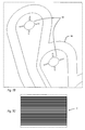
- FIG. 7 shows two laterally spaced longitudinally extending multiconductor microcircuits machined by laser cutting the metallic ribbon attached to the upper surface of the film substrate shown in FIG. 6 , each microcircuit including a flat elongated multiconductor tail portion with longitudinally spaced outwardly exposed ring electrode receiving pads and a flat multiconductor arc-shaped head portion with spaced circuit attachment or interconnect pads as shown more clearly in FIG. 7A and FIG. 7B respectively, FIG. 7C showing the close lateral spacing of laser cut individual conductors in the tail portion of the microcircuits.
- FIG. 8 shows the carrier and microcircuits of FIG. 7 clamped to a base of a heated ceramic vacuum chuck prior to overmolding with a silicone layer.
- FIG. 9 shows the carrier and chuck of FIG. 8 with an overmold plate covering the carrier and including lower features that shut-off and create exposed areas on the ring electrode receiving pads and interconnect pads.
- FIG. 10 shows the carrier and microcircuits of FIG. 8 after the overmolding step has been completed and the microcircuits are laminated between the silicone layer and the film substrate.
- FIG. 11 shows the carrier and laminated microcircuits removed from the ceramic vacuum chuck of FIGS. 8-10 .
- FIG. 12 shows the microcircuits completely excised from the carrier as by laser cutting through both the silicone and film substrate layers.
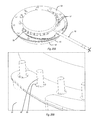
- FIG. 13A shows the head portion of one of the microcircuits clamped to a tooling bow having a tensioned wire extending between ends of the bow and used first to receive a series of platinum electrode rings and then after tensioning by the bow to receive the tail of the microcircuit as it is wrapped into a helical shape and to suspend the microcircuit during subsequent overmolding processes.
- FIG. 13B shows the head portion of the microcircuit extending from the tensioned wire of the tooling bow and the tail portion wrapped in a helix around the tensioned wire with the ring electrode receiving pads exposed on an outer surface of the helix.
- FIG. 14A shows the head and tail portions of the microcircuit as illustrated in FIG. 13B with a ring electrode being positioned over an exposed receiving pad of the microcircuit.
- FIG. 14B shows a series of ring electrodes on the helically wrapped tail portion of the microcircuit each ring being positioned over a different electrode receiving pad with a hole in the ring electrode aligned with its supporting pad for future laser welding to the pad.
- FIG. 14C in an enlarged showing of a portion of the helically wrapped portion of FIG. 14B depicting each electrode as laser welded to its supporting pad.
- FIG. 15 shows the microcircuit supported on the tensioning wire of the tooling bow after a first overmold that encapsulates the wrapped electrode up to its first ring electrode and the underneath of the interconnect circuit of the head portion of the microcircuit creating a silicone stand-off for the head portion.
- FIG. 16 shows the microcircuit supported on the tensioning wire of the tooling bow after a second overmold that encapsulates the wrapped electrode out to the end of the electrode subassembly with the overmold decreasing in diameter as it approaches the first visible ring electrode.
- FIG. 17A shows the overmolded electrode subassembly of FIG. 16 after completion of a third overmolding process that was preceded by the subassembly having been removed from the tooling bow and an end of the microcircuit unwrapped offsetting the electrode and creating a stylet lumen into which a stylet was placed and the electrode and stylet placed into overmold tooling for overmolding.
- FIG. 17B is an enlarged showing of a portion of the electrode assembly of FIG. 17A including the unwrapped microcircuit and stylet lumen.
- FIG. 18A a conventional stylet insertion tool inserted into the lumen of the electrode subassembly straightening the electrode for insertion.
- FIG. 18B shows the stylet insertion tool rotated 90 degrees to show the handle of the tool.
- FIG. 19 shows the completed helix electrode assembly ready for attachment of its head portion to the platinum feedthrough posts of a titanium housing as shown in FIGS. 20A and 20B .
- FIGS. 20A and 20B show a titanium housing where the microcircuit interconnect pads slit slightly during laser machining make intimate contact with corresponding ones of the feedthrough posts for laser welding to the posts.
- the process of the present invention is intended to efficiently produce a new and improved microcircuit integrated cochlear electrode array 10 , that comprises multiconductor microcircuit 12 including a multiconductor tail portion 14 with longitudinally spaced outwardly exposed electrode receiving pads 16 (see FIGS. 7A and 12 ) and a flat multiconductor head portion 18 connected to the tail portion and having spaced outwardly exposed circuit attachment pads 20 (see FIGS. 13B , 15 , 19 , 20 A and 20 B).
- the tail and head portions 14 and 18 are laminated between a nonconductive film substrate 22 (see FIGS. 3-5 ) and an insulating cover 24 (see FIG. 10 ).
- FIGS. 3-5 nonconductive film substrate 22
- an insulating cover 24 see FIG. 10
- the tail portion 14 is helically wrapped into a helix with the electrode receiving circuit attachment pads 16 exposed to and carrying ring electrodes 26 overmolded with a plastic material 28 (see FIG. 17A ).
- a portion of the tail portion 14 may be unwrapped at a junction 58 with a section 60 including the ring electrodes 62 offsetting an electrode section 49 and creating a lumen 62 for receiving a stylet 64 as shown in FIGS. 18A and 18B .
- the process of the present invention basically comprises the steps of the flow diagram of FIG. 1A .
- the process comprises securing and supporting the nonconductive film substrate 22 ; attaching a metallic ribbon 30 to a surface of the substrate 22 ; machining at least one flat multiconductor microcircuit 12 from the ribbon 30 including the flat elongated multiconductor tail portion 14 with longitudinally spaced outwardly exposed ring electrode receiving pads 16 and the flat multiconductor head portion 18 connected to the tail portion and having spaced outwardly exposed attachment pads 20 ; laminating the flat microcircuit 12 between the film substrate 22 and the insulating cover 24 ; excising the laminated microcircuit 12 from the film substrate 22 with the electrode receiving pads 20 exposed; helically wrapping the tail portion 14 of the excised laminated microcircuit 12 into a helix with the exposed electrode receiving pads 16 wrapped around the insulating cover 24 ; mounting and electrically connecting the ring
- a roll 32 of the nonconductive film substrate 22 is positioned adjacent an end of a lower open frame 34 of a carrier 36 utilized in the process steps of securing and supporting the nonconductive film substrate.
- a length of the film substrate 22 is drawn from the roll 32 to extend over the top of the open frame 34 .
- the film substrate 22 is maintained under tension in both X and Y directions while positioned over the open frame.
- the length of film substrate 22 is then moved downward relative to the lower open frame 34 until attachment means 38 , such as upwardly projecting pins 39 , engage and penetrate a lower surface of the film substrate securing the tensioned length of film substrate 22 to the lower open frame.
- attachment means 38 such as upwardly projecting pins 39
- an upper open frame 40 of the carrier 36 is then positioned over and on the lower open frame 34 with alignment holes 41 in the upper frame receiving alignment pins 35 extending upward from the lower frame 34 and the upper frame secured to the lower frame as by screws clamping the length of tensioned film substrate within the carrier 36 . Excess film is then trimmed from the carrier 36 and separated from the roll 32 of plastic as depicted in FIG. 5 .
- the next step in the process of the present invention is the attachment of the flat metallic ribbon 30 to a surface of the film substrate 22 shown in FIG. 6 .
- the carrier 36 and the metallic ribbon 30 preferably a platinum iridium ribbon
- the carrier 36 and the etched platinum ribbon 30 are then placed into a standard thermal heating fixture (not shown) with tooling liners located on the carrier.
- the platinum ribbon 30 is carefully placed into a transfer fixture (not shown) so that the ribbon is aligned relative to the tooling liners located on the carrier 36 .
- the ribbon 30 is lowered onto the etched surface of the film substrate 22 where pressure and heat are applied for a prescribed time period to secure the ribbon to the film substrate.
- FIGS. 7 , 7 A and 7 B depicting the spacing of the parallel laser machined conductors of the two microcircuits 12 as being approximately 25 micron in width with 25 micron kerfs between the conductors.
- the machining is achieved using laser machining with a femtosecond impulse laser machining center such as the commercially available Clark-MXR Femtosecond Impulse Laser Machining Center.
- Femtosecond laser light pulses are about one quadrillionth of a second in time duration and bypass the material melt phase and transition directly into the vapor phase thus creating very little heat and no slag or damage to surrounding areas. Also, femtosecond light pulses are capable of creating sub-micron features down to 50 nm and are wavelength independent and capable of machining any material.
- the upper surface of the platinum ribbon is plasma etched and the carrier 36 is placed on a conventional heated ceramic vacuum chuck 42 and clamped in place as shown in FIG. 8 for conventional overmolding and lamination of the microcircuits between the film substrate 22 and the previously referenced insulating cover 24 .
- an overmolding mold plate 44 is installed over the exposed microcircuits 12 using tooling pins (not shown) located on a top cover of the carrier 36 .
- the mold plate 44 is designed with shut-off features that will expose the ring electrode receiving pads 16 and the interconnect pads 20 during the subsequent operation of the heated vacuum chuck 42 and lamination of the microcircuits between the film substrate 22 and the insulating cover 24 . Accordingly, when the heated ceramic vacuum chuck 42 and the enclosed carrier 36 reach a prescribed temperature, de-gassed silicone is injected between the carrier 36 and the mold plate 44 and a thin film of silicone comprising the insulating cover 24 is created around and between the features of the microcircuits 12 while the ring electrode receiving pads 16 of the tail portion 14 and the interconnect pads 20 of the head portion 18 remain exposed as depicted in FIGS. 10 and 11 .
- FIG. 10 shows the assembly of FIG. 9 with the mold plate 44 removed.
- insulating cover 24 may be provided by laminating a second layer of film onto the microcircuits 12 , adhering the second film layer to the microcircuits and to the exposed portions of film substrate 22 .
- the carrier 36 is placed in a femtosecond laser excising machine (not shown) and using the vision system built into the laser, the microcircuits are accurately aligned within the laser.
- the laser is then activated to cut completely through the silicone and nonconductive film layers comprising the insulating cover 24 and the film substrate 22 completely freeing the microcircuits 12 from the carrier 36 as depicted in FIG. 12 .
- FIG. 13A Further processing operations of the process of the present invention preferably utilize a tooling bow 46 and a tensioned arbor wire 48 extending between opposite free ends of the bow as depicted in FIG. 13A .
- the tensioned arbor wire is used to wrap the tail portion 14 of one of the newly created microcircuits 12 into a helical shape and also suspend the electrode assembly 10 through various overmolding processes as will be described below.
- a series of the platinum electrode rings 26 are threaded onto the wire 48 prior to its tensioning on the bow.
- the head portion 18 of one of the microcircuits 12 is then threaded onto the arbor wire 48 and clamped in place leaving the tail portion 14 of the microcircuit 12 free to be manually wrapped on the arbor wire 48 .
- the tail portion 14 is then manually rotated around the arbor wire 48 such that edges of the silicone cover (or second film layer) 24 and film substrate 22 contact each other and the tail portion 14 forms a helix on the arbor wire 48 as shown in FIG. 13B .
- FIG. 13B shows the head portion of the microcircuit extending from the tensioned wire of the tooling bow and the tail portion wrapped in a helix around the tensioned wire with the ring electrode receiving pads exposed on an outer surface of the helix.
- the exposed ring electrode receiving pads 16 are wrapped around the silicone cover 24 in proper location or pitch along the tail portion of the microcircuit 12 .
- the platinum electrode rings 26 pre-mounted on the arbor wire 48 are positioned by an operator one at a time on the wrapped and exposed receiving pads 16 with radially extending holes 27 the electrode rings aligned with the pads for future laser welding of the rings to the pads as depicted in FIGS. 14A-C .
- the tooling bow 46 is placed into a standard laser welding machine (not shown) where each electrode ring 26 and hole 27 is located by the laser vision system of the laser welding machine. The laser will then weld each ring 26 to each pad 16 at its ring hole 27 and the process repeated until all of the electrodes are welded in place.
- the wrapped electrode subassembly is plasma etched and the preformed microcircuit 12 placed into overmolding mold tooling.
- a section 49 of the wrapped electrode up to a first inactive visual electrode and the underside of the head portion 18 shown in FIG. 15 are then encapsulated with a silicone film 50 (comprising the overmolded plastic material 28 ) by overmolding apparatus such as described and illustrated in FIG. 9 .
- the overmolding of the underside of the head portion 18 acts as reinforcing for the interconnect circuit and pads 20 and creates a stand-off that may be used for height referencing when attaching the microcircuit 12 to posts 52 extending vertically from a titanium housing 54 as shown in FIGS. 20 A and 20 B.
- the tooling bow 46 is mounted in overmold tooling and placed in overmold apparatus such as described and illustrated in FIG. 9 .
- a section 60 of the wrapped microcircuit 12 shown in FIG. 16 between the overmold of FIG. 15 and the microcircuit section including the spaced ring electrodes is then encapsulated in a silicone film 56 depicted in FIG. 16 .
- the film 56 in section 60 is feathered down in size creating a smaller diameter of about 0.025 inches approximately 0.80 inches from the first inactive visual platinum electrode shown in FIG. 15 .
- the preformed and overmolded electrode is removed from the tooling bow 46 .
- the electrode is then unwrapped at a junction 58 with section 60 including the spaced ring electrodes, offsetting the electrode section 60 including the spaced ring electrodes and creating a stylet lumen 62 .
- a stylet 64 is inserted in the lumen 62 as illustrated in FIGS. 18A and 18B to straighten the electrode section 60 and the electrode and stylet are placed in an overmold apparatus similar to that shown and described relative to FIG. 9 where a silicone film 61 is formed encapsulating the electrode section 60 .
- the completed electrode is then placed in a post-curing oven for final curing of the completed electrode assembly.
- the electrode section When the stylet 64 is removed from the lumen 62 , the electrode section will assume the spiral shape shown in FIG. 17A .
- the stylet 64 is re-inserted in the lumen 62 using a conventional stylet insertion tool 66 such as shown in FIG. 18A , FIG. 18B showing the insertion tool 66 rotated 90 degrees to illustrate the handle 67 of the tool.
- FIG. 19 shows the completed helix electrode assembly 10 ready for attachment of its head portion 18 to the platinum feedthrough posts 52 of the titanium housing 54 as shown in FIGS. 20A and 20B where the microcircuit interconnect or attachment pads 20 are slit slightly during laser machining to make intimate contact with corresponding ones of the feedthrough posts for laser welding to the posts.
Abstract
Description
Claims (10)
Priority Applications (3)
| Application Number | Priority Date | Filing Date | Title |
|---|---|---|---|
| US12/338,758 US8250745B1 (en) | 2008-01-24 | 2008-12-18 | Process for manufacturing a microcircuit cochlear electrode array |
| US13/556,896 US8897894B1 (en) | 2008-01-24 | 2012-07-24 | Microcircuit cochlear electrode array and method of manufacture |
| US14/474,806 US9402991B1 (en) | 2008-01-24 | 2014-09-02 | Microcircuit cochlear electrode array and method of manufacture |
Applications Claiming Priority (2)
| Application Number | Priority Date | Filing Date | Title |
|---|---|---|---|
| US2338908P | 2008-01-24 | 2008-01-24 | |
| US12/338,758 US8250745B1 (en) | 2008-01-24 | 2008-12-18 | Process for manufacturing a microcircuit cochlear electrode array |
Related Child Applications (1)
| Application Number | Title | Priority Date | Filing Date |
|---|---|---|---|
| US13/556,896 Division US8897894B1 (en) | 2008-01-24 | 2012-07-24 | Microcircuit cochlear electrode array and method of manufacture |
Publications (1)
| Publication Number | Publication Date |
|---|---|
| US8250745B1 true US8250745B1 (en) | 2012-08-28 |
Family
ID=46689625
Family Applications (3)
| Application Number | Title | Priority Date | Filing Date |
|---|---|---|---|
| US12/338,758 Active 2030-07-06 US8250745B1 (en) | 2008-01-24 | 2008-12-18 | Process for manufacturing a microcircuit cochlear electrode array |
| US13/556,896 Active US8897894B1 (en) | 2008-01-24 | 2012-07-24 | Microcircuit cochlear electrode array and method of manufacture |
| US14/474,806 Active 2029-02-07 US9402991B1 (en) | 2008-01-24 | 2014-09-02 | Microcircuit cochlear electrode array and method of manufacture |
Family Applications After (2)
| Application Number | Title | Priority Date | Filing Date |
|---|---|---|---|
| US13/556,896 Active US8897894B1 (en) | 2008-01-24 | 2012-07-24 | Microcircuit cochlear electrode array and method of manufacture |
| US14/474,806 Active 2029-02-07 US9402991B1 (en) | 2008-01-24 | 2014-09-02 | Microcircuit cochlear electrode array and method of manufacture |
Country Status (1)
| Country | Link |
|---|---|
| US (3) | US8250745B1 (en) |
Cited By (3)
| Publication number | Priority date | Publication date | Assignee | Title |
|---|---|---|---|---|
| US10058698B2 (en) | 2013-08-27 | 2018-08-28 | Advanced Bionics Ag | Asymmetric cochlear implant electrodes and method |
| US10058699B2 (en) | 2013-08-27 | 2018-08-28 | Advanced Bionics Ag | Implantable leads with flag extensions |
| US10058697B2 (en) | 2013-08-27 | 2018-08-28 | Advanced Bionics Ag | Thermoformed electrode arrays |
Families Citing this family (2)
| Publication number | Priority date | Publication date | Assignee | Title |
|---|---|---|---|---|
| US8250745B1 (en) * | 2008-01-24 | 2012-08-28 | Advanced Bionics, Llc | Process for manufacturing a microcircuit cochlear electrode array |
| US11439832B2 (en) * | 2019-01-09 | 2022-09-13 | Stimwave Technologies Incorporated | Implantable electronic devices |
Citations (59)
| Publication number | Priority date | Publication date | Assignee | Title |
|---|---|---|---|---|
| US4031310A (en) | 1975-06-13 | 1977-06-21 | General Cable Corporation | Shrinkable electrical cable core for cryogenic cable |
| EP0002068A2 (en) | 1977-11-22 | 1979-05-30 | Carl Christian Hansen | Electrode for implantation into cochlea |
| EP0007157A2 (en) | 1978-05-04 | 1980-01-23 | The University Of Melbourne | Improved electrode array and method of making the same |
| US4261372A (en) | 1977-11-22 | 1981-04-14 | Hansen Carl C | Electrode for implantation into cochlea |
| US4762135A (en) | 1985-08-30 | 1988-08-09 | Puije P D V D | Cochlea implant |
| US4832051A (en) | 1985-04-29 | 1989-05-23 | Symbion, Inc. | Multiple-electrode intracochlear device |
| US5580699A (en) | 1994-08-16 | 1996-12-03 | Ventritex, Inc. | Method for manufacturing implantable cardiac defibrillation electrodes using a laser beam material removal process |
| WO1997006760A1 (en) | 1995-08-18 | 1997-02-27 | Pi Medical Corporation | Multi-electrode cochlear implant |
| WO1997028668A1 (en) | 1996-01-31 | 1997-08-07 | Cochlear Limited | Thin film fabrication technique for implantable electrodes |
| US5987361A (en) | 1996-03-07 | 1999-11-16 | Axon Engineering, Inc. | Polymer-metal foil structure for neural stimulating electrodes |
| US6309410B1 (en) * | 1998-08-26 | 2001-10-30 | Advanced Bionics Corporation | Cochlear electrode with drug delivery channel and method of making same |
| US6355401B1 (en) | 1997-11-07 | 2002-03-12 | Intermedics Inc. | Method for preparing a high definition window in a conformally coated medical device |
| US6374143B1 (en) | 1999-08-18 | 2002-04-16 | Epic Biosonics, Inc. | Modiolar hugging electrode array |
| US6421569B1 (en) * | 1999-05-21 | 2002-07-16 | Cochlear Limited | Cochlear implant electrode array |
| WO2002078575A1 (en) | 2001-03-29 | 2002-10-10 | Cochlear Limited | Laminated electrode for a cochlear implant |
| WO2002089907A1 (en) | 2001-05-07 | 2002-11-14 | Cochlear Limited | Process for manufacturing electrically conductive components |
| WO2003017329A2 (en) | 2001-08-17 | 2003-02-27 | Advanced Cochlear Systems, Inc. | High contact density planar array |
| US20030097165A1 (en) | 2001-11-16 | 2003-05-22 | The Regents Of The University Of California. | Flexible electrode array for artificial vision |
| WO2003049638A2 (en) | 2001-12-06 | 2003-06-19 | Advanced Cochlear Systems, Inc. | Bio-implant and method of making the same |
| US6643552B2 (en) | 2001-05-30 | 2003-11-04 | Foster-Miller, Inc. | Implantable devices having a liquid crystal polymer substrate |
| WO2003090848A1 (en) | 2002-04-23 | 2003-11-06 | Cochlear Limited | Electrode array for a cochlear implant having one or more adjustable electrodes |
| US20030236562A1 (en) | 2000-10-10 | 2003-12-25 | Kuzma Janusz A. | Band type multicontact electrode and method of making the same |
| US20040020686A1 (en) | 2002-08-01 | 2004-02-05 | Sanchez Alfonso Perez | Superconducting power cable with enhanced superconducting core |
| WO2004035133A1 (en) | 2002-10-17 | 2004-04-29 | Cochlear Limited | Implantable conducting lead |
| WO2004054474A1 (en) | 2002-12-18 | 2004-07-01 | Instituto Científico Y Tecnológico De Navarra S.A. | Electrode-bearing guide, cochlear implant comprising said guide and production method thereof |
| US6757970B1 (en) | 2000-11-07 | 2004-07-06 | Advanced Bionics Corporation | Method of making multi-contact electrode array |
| US20040147992A1 (en) | 2003-01-23 | 2004-07-29 | Epic Biosonics Inc. | Implantable medical assembly |
| US6779257B2 (en) | 1999-03-03 | 2004-08-24 | Volcano Therapeutics, Inc. | Method of making a flexible elongate member |
| US20040256146A1 (en) | 2003-06-17 | 2004-12-23 | W.C. Heraeus Gmbh & Co., Kg | Electrode structure and methods for producing and using the same |
| US6843870B1 (en) | 2003-07-22 | 2005-01-18 | Epic Biosonics Inc. | Implantable electrical cable and method of making |
| WO2005004978A1 (en) | 2003-07-09 | 2005-01-20 | Cochlear Limited | Conductive elements |
| US20050256561A1 (en) | 2002-06-28 | 2005-11-17 | Gantz Bruce J | Cochlear implant electrode array |
| US6974533B2 (en) | 2002-04-11 | 2005-12-13 | Second Sight Medical Products, Inc. | Platinum electrode and method for manufacturing the same |
| US20060003090A1 (en) | 2004-05-14 | 2006-01-05 | California Institute Of Technology | Parylene-based flexible multi-electrode arrays for neuronal stimulation and recording and methods for manufacturing the same |
| WO2006000031A1 (en) | 2004-06-25 | 2006-01-05 | Cochlear Limited | Electrode assembly |
| US20060095105A1 (en) | 2001-10-31 | 2006-05-04 | London Health Sciences Center | Multichannel electrode and methods of using same |
| US7067765B2 (en) | 2004-08-23 | 2006-06-27 | Medtronic, Inc. | Methods for forming electrically active surfaces for medical electrical leads |
| US20060247754A1 (en) | 2005-04-28 | 2006-11-02 | Robert Greenberg | Flexible circuit electrode array |
| US20060255293A1 (en) | 2005-04-21 | 2006-11-16 | California Institute Of Technology | Method for decreasing chemical diffusion in parylene and trapping at parylene-to-parylene interfaces |
| US7142909B2 (en) | 2002-04-11 | 2006-11-28 | Second Sight Medical Products, Inc. | Biocompatible bonding method and electronics package suitable for implantation |
| US20070123963A1 (en) | 2005-11-29 | 2007-05-31 | Peter Krulevitch | Method for producing flexible, stretchable, and implantable high-density microelectrode arrays |
| WO2007065216A2 (en) | 2005-12-06 | 2007-06-14 | Cochlear Limited | Cochlear implant assembly |
| US20070168004A1 (en) | 2005-12-01 | 2007-07-19 | Advanced Bionics Corporation | Cylindrical multi-contact electrode lead for neural stimulation and method of making same |
| US20070293749A1 (en) | 2006-06-19 | 2007-12-20 | Zhou Dao M | Electrode with increased stability and method of manufacturing the same |
| WO2008011721A1 (en) | 2006-07-28 | 2008-01-31 | Med-El Elektro-Medizinische Geräte Gesellschaft M.B.H. | Layered electrode array and cable |
| US20080044591A1 (en) | 2006-06-06 | 2008-02-21 | Laude Lucien D | Molded Polymer Comprising Silicone and at Least One Metal Trace and a Process of Manufacturing the Same |
| WO2008031144A1 (en) | 2006-09-12 | 2008-03-20 | Cochlear Limited | Implantable electrode array |
| US20080262584A1 (en) | 2007-03-19 | 2008-10-23 | Bottomley Paul A | Methods and apparatus for fabricating leads with conductors and related flexible lead configurations |
| WO2009062114A2 (en) | 2007-11-08 | 2009-05-14 | Second Sight Medical Products, Inc. | Cochlear stimulation device comprising a flexible electrode array |
| WO2009065127A1 (en) | 2007-11-16 | 2009-05-22 | Cochlear Americas | Electrode array and method of forming an electrode array |
| WO2009065171A1 (en) | 2007-11-19 | 2009-05-28 | Cochlear Limited | Electrode array for a cochlear implant |
| US7587248B2 (en) | 2004-04-19 | 2009-09-08 | Cochlear Limited | Implantable prosthetic device |
| EP2066397B1 (en) | 2006-08-24 | 2010-02-17 | Med-El Elektromedizinische Geräte Gesellschaft m.b.H. | Multi-channel electrode for cochlea implants, with a plurality of contacts distributed along the length of the electrode |
| WO2010055421A1 (en) | 2008-11-12 | 2010-05-20 | Aleva Neurotherapeutics, S.A. | Microfabricated neurostimulation device |
| WO2010079875A1 (en) | 2009-01-07 | 2010-07-15 | Snu R&Db Foundation | Micro-electrode array package using liquid crystal polymer and manufacturing method thereof |
| WO2010138567A2 (en) | 2009-05-27 | 2010-12-02 | Med-El Elektromedizinische Geraete Gmbh | Ink jet printing of implantable electrodes |
| US20110098719A1 (en) | 2009-10-28 | 2011-04-28 | New York University | Cochlear implant with improved electrode array and controller |
| US20110180305A1 (en) | 2010-01-22 | 2011-07-28 | The Regents Of The University Of Michigan | Electrode array and method of fabrication |
| WO2012003297A1 (en) | 2010-06-30 | 2012-01-05 | Med-El Elektromedizinische Geraete Gmbh | Helical core ear implant electrode |
Family Cites Families (12)
| Publication number | Priority date | Publication date | Assignee | Title |
|---|---|---|---|---|
| FR2629710B1 (en) * | 1988-04-08 | 1997-10-24 | Mxm | ELECTRODE HOLDER DEVICES IMPLANTABLE IN THE COCHLEE FOR ELECTRICALLY STIMULATING THE HEARING NERVE |
| US5344387A (en) | 1992-12-23 | 1994-09-06 | Lupin Alan J | Cochlear implant |
| US6074422A (en) | 1998-04-22 | 2000-06-13 | Epic Biosonics Inc. | Inner ear implant device |
| US6163729A (en) * | 1998-08-26 | 2000-12-19 | Advanced Bionics Corporation | Method of positioning an implantable cochlear electrode array within a cochlea |
| AU2003901146A0 (en) * | 2003-03-12 | 2003-03-27 | Cochlear Limited | Feedthrough assembly |
| US7035692B1 (en) | 2003-04-30 | 2006-04-25 | The Regents Of The University Of California | High density polymer-based integrated electrode array |
| US8147486B2 (en) * | 2003-09-22 | 2012-04-03 | St. Jude Medical, Atrial Fibrillation Division, Inc. | Medical device with flexible printed circuit |
| US7750076B2 (en) | 2006-06-07 | 2010-07-06 | Second Sight Medical Products, Inc. | Polymer comprising silicone and at least one metal trace |
| US8250745B1 (en) * | 2008-01-24 | 2012-08-28 | Advanced Bionics, Llc | Process for manufacturing a microcircuit cochlear electrode array |
| JP4793389B2 (en) | 2008-02-04 | 2011-10-12 | 株式会社大林組 | Construction method of joint part of underground wall, underground wall |
| US8382943B2 (en) | 2009-10-23 | 2013-02-26 | William George Clark | Method and apparatus for the selective separation of two layers of material using an ultrashort pulse source of electromagnetic radiation |
| US8332052B1 (en) * | 2010-03-18 | 2012-12-11 | Advanced Bionics | Microcircuit cochlear electrode array and method of manufacture |
-
2008
- 2008-12-18 US US12/338,758 patent/US8250745B1/en active Active
-
2012
- 2012-07-24 US US13/556,896 patent/US8897894B1/en active Active
-
2014
- 2014-09-02 US US14/474,806 patent/US9402991B1/en active Active
Patent Citations (102)
| Publication number | Priority date | Publication date | Assignee | Title |
|---|---|---|---|---|
| US4031310A (en) | 1975-06-13 | 1977-06-21 | General Cable Corporation | Shrinkable electrical cable core for cryogenic cable |
| EP0002068A2 (en) | 1977-11-22 | 1979-05-30 | Carl Christian Hansen | Electrode for implantation into cochlea |
| US4261372A (en) | 1977-11-22 | 1981-04-14 | Hansen Carl C | Electrode for implantation into cochlea |
| US4284085A (en) | 1977-11-22 | 1981-08-18 | Hansen Carl C | Electrode for implantation into the cochlea (II) |
| EP0007157A2 (en) | 1978-05-04 | 1980-01-23 | The University Of Melbourne | Improved electrode array and method of making the same |
| US4832051A (en) | 1985-04-29 | 1989-05-23 | Symbion, Inc. | Multiple-electrode intracochlear device |
| US4762135A (en) | 1985-08-30 | 1988-08-09 | Puije P D V D | Cochlea implant |
| US5658709A (en) | 1994-08-16 | 1997-08-19 | Ventritex, Inc. | Method for manufacturing implantable cardiac defibrillation electrodes using a laser beam material removal process |
| US5580699A (en) | 1994-08-16 | 1996-12-03 | Ventritex, Inc. | Method for manufacturing implantable cardiac defibrillation electrodes using a laser beam material removal process |
| WO1997006760A1 (en) | 1995-08-18 | 1997-02-27 | Pi Medical Corporation | Multi-electrode cochlear implant |
| WO1997028668A1 (en) | 1996-01-31 | 1997-08-07 | Cochlear Limited | Thin film fabrication technique for implantable electrodes |
| US5720099A (en) | 1996-01-31 | 1998-02-24 | Cochlear Limited | Thin film fabrication technique for implantable electrodes |
| EP0888701B1 (en) | 1996-01-31 | 2007-10-03 | Cochlear Limited | Thin film fabrication technique for implantable electrodes |
| US5987361A (en) | 1996-03-07 | 1999-11-16 | Axon Engineering, Inc. | Polymer-metal foil structure for neural stimulating electrodes |
| US6355401B1 (en) | 1997-11-07 | 2002-03-12 | Intermedics Inc. | Method for preparing a high definition window in a conformally coated medical device |
| US6309410B1 (en) * | 1998-08-26 | 2001-10-30 | Advanced Bionics Corporation | Cochlear electrode with drug delivery channel and method of making same |
| US6779257B2 (en) | 1999-03-03 | 2004-08-24 | Volcano Therapeutics, Inc. | Method of making a flexible elongate member |
| US6421569B1 (en) * | 1999-05-21 | 2002-07-16 | Cochlear Limited | Cochlear implant electrode array |
| US6374143B1 (en) | 1999-08-18 | 2002-04-16 | Epic Biosonics, Inc. | Modiolar hugging electrode array |
| US20040015221A1 (en) | 2000-10-10 | 2004-01-22 | Kuzma Janusz A. | Band type multicontact electrode and method of making the same |
| US20030236562A1 (en) | 2000-10-10 | 2003-12-25 | Kuzma Janusz A. | Band type multicontact electrode and method of making the same |
| US7047081B2 (en) | 2000-10-10 | 2006-05-16 | Advanced Bionics Corporation | Band type multicontact electrode and method of making the same |
| US6757970B1 (en) | 2000-11-07 | 2004-07-06 | Advanced Bionics Corporation | Method of making multi-contact electrode array |
| US7406352B2 (en) | 2001-03-29 | 2008-07-29 | Cochlear Limited | Laminated electrode for a cochlear implant |
| US20040172118A1 (en) | 2001-03-29 | 2004-09-02 | Peter Gibson | Laminated electrode for a cochlear implant |
| WO2002078575A1 (en) | 2001-03-29 | 2002-10-10 | Cochlear Limited | Laminated electrode for a cochlear implant |
| US20040147825A1 (en) | 2001-05-07 | 2004-07-29 | Dusan Milojevic | Process for manufacturing electrically conductive components |
| WO2002089907A1 (en) | 2001-05-07 | 2002-11-14 | Cochlear Limited | Process for manufacturing electrically conductive components |
| US7240416B2 (en) | 2001-05-07 | 2007-07-10 | Cochlear Limited | Process for manufacturing electrically conductive components |
| US7970481B2 (en) | 2001-05-07 | 2011-06-28 | Cochlear Limited | Process for manufacturing electronically conductive components |
| US20100287762A1 (en) | 2001-05-07 | 2010-11-18 | Dusan Milojevic | Process for manufacturing electronically conductive components |
| US6643552B2 (en) | 2001-05-30 | 2003-11-04 | Foster-Miller, Inc. | Implantable devices having a liquid crystal polymer substrate |
| US6782619B2 (en) | 2001-08-17 | 2004-08-31 | Advanced Cochlear Systems, Inc. | Method of making high contact density electrode array |
| WO2003017329A3 (en) | 2001-08-17 | 2003-07-10 | Advanced Cochlear Sys Inc | High contact density planar array |
| WO2003017329A2 (en) | 2001-08-17 | 2003-02-27 | Advanced Cochlear Systems, Inc. | High contact density planar array |
| US20060095105A1 (en) | 2001-10-31 | 2006-05-04 | London Health Sciences Center | Multichannel electrode and methods of using same |
| US20030097165A1 (en) | 2001-11-16 | 2003-05-22 | The Regents Of The University Of California. | Flexible electrode array for artificial vision |
| US6678564B2 (en) | 2001-12-06 | 2004-01-13 | Advanced Cochlear Systems, Inc. | Bio-implant and method of making the same |
| WO2003049638A2 (en) | 2001-12-06 | 2003-06-19 | Advanced Cochlear Systems, Inc. | Bio-implant and method of making the same |
| WO2003049638A3 (en) | 2001-12-06 | 2004-04-22 | Advanced Cochlear Sys Inc | Bio-implant and method of making the same |
| US6974533B2 (en) | 2002-04-11 | 2005-12-13 | Second Sight Medical Products, Inc. | Platinum electrode and method for manufacturing the same |
| US7142909B2 (en) | 2002-04-11 | 2006-11-28 | Second Sight Medical Products, Inc. | Biocompatible bonding method and electronics package suitable for implantation |
| WO2003090848A1 (en) | 2002-04-23 | 2003-11-06 | Cochlear Limited | Electrode array for a cochlear implant having one or more adjustable electrodes |
| US20060089700A1 (en) | 2002-04-23 | 2006-04-27 | Darley Derek I | Electrode array for a cochlear implant having one or more adjustable electrodes |
| US20050256561A1 (en) | 2002-06-28 | 2005-11-17 | Gantz Bruce J | Cochlear implant electrode array |
| US20040020686A1 (en) | 2002-08-01 | 2004-02-05 | Sanchez Alfonso Perez | Superconducting power cable with enhanced superconducting core |
| US20060206185A1 (en) | 2002-10-17 | 2006-09-14 | Cochlear Limited | Implantable conducting lead |
| WO2004035133A1 (en) | 2002-10-17 | 2004-04-29 | Cochlear Limited | Implantable conducting lead |
| US7774071B2 (en) | 2002-10-17 | 2010-08-10 | Cochlear Limited | Implantable conducting lead |
| WO2004054474A1 (en) | 2002-12-18 | 2004-07-01 | Instituto Científico Y Tecnológico De Navarra S.A. | Electrode-bearing guide, cochlear implant comprising said guide and production method thereof |
| EP1574181A1 (en) | 2002-12-18 | 2005-09-14 | Instituto Cientifico Y Tecnologico De Navarra, S.A. | Electrode-bearing guide, cochlear implant comprising said guide and production method thereof |
| US20080140156A1 (en) | 2002-12-18 | 2008-06-12 | Manuel Manrique Rodriguez | Electrode-Bearing Guide, Cochlear Implant Comprising Said Guide and Production Method Thereof |
| EP1574181B1 (en) | 2002-12-18 | 2010-10-20 | Instituto Cientifico Y Tecnologico De Navarra, S.A. | Electrode-bearing guide, cochlear implant comprising said guide and production method thereof |
| US20040147992A1 (en) | 2003-01-23 | 2004-07-29 | Epic Biosonics Inc. | Implantable medical assembly |
| EP1587454B1 (en) | 2003-01-23 | 2010-04-14 | Med-El Elektro-Medizinische Geräte Gesellschaft m.b.H. | Implantable medical assembly using a corrugated film |
| US7085605B2 (en) | 2003-01-23 | 2006-08-01 | Epic Biosonics Inc. | Implantable medical assembly |
| WO2004064687A1 (en) | 2003-01-23 | 2004-08-05 | Epic Biosonics, Inc. | Implantable medical assembly using a corrugated film |
| US20040256146A1 (en) | 2003-06-17 | 2004-12-23 | W.C. Heraeus Gmbh & Co., Kg | Electrode structure and methods for producing and using the same |
| US20080027525A1 (en) | 2003-06-17 | 2008-01-31 | W. C. Heraeus Gmbh & Co., Kg | Electrode Structure |
| US20060236532A1 (en) | 2003-07-09 | 2006-10-26 | Cochlear Limited | Conductive elements |
| US20090229739A1 (en) | 2003-07-09 | 2009-09-17 | Cochlear Limited | Conductive elements |
| WO2005004978A1 (en) | 2003-07-09 | 2005-01-20 | Cochlear Limited | Conductive elements |
| US20050107858A1 (en) | 2003-07-22 | 2005-05-19 | Epic Biosonics Inc. | Implantable electrical cable and method of making |
| US20050016657A1 (en) | 2003-07-22 | 2005-01-27 | Epic Biosonics Inc. | Implantable electrical cable and method of making |
| US6843870B1 (en) | 2003-07-22 | 2005-01-18 | Epic Biosonics Inc. | Implantable electrical cable and method of making |
| EP1651305B1 (en) | 2003-07-22 | 2011-08-10 | Med-El Elektromedizinische Geräte Gesellschaft m.b.H. | Implantable electrical cable and method of making |
| US7587248B2 (en) | 2004-04-19 | 2009-09-08 | Cochlear Limited | Implantable prosthetic device |
| US20060003090A1 (en) | 2004-05-14 | 2006-01-05 | California Institute Of Technology | Parylene-based flexible multi-electrode arrays for neuronal stimulation and recording and methods for manufacturing the same |
| US7326649B2 (en) | 2004-05-14 | 2008-02-05 | University Of Southern California | Parylene-based flexible multi-electrode arrays for neuronal stimulation and recording and methods for manufacturing the same |
| WO2006000031A1 (en) | 2004-06-25 | 2006-01-05 | Cochlear Limited | Electrode assembly |
| US20090043358A1 (en) | 2004-06-25 | 2009-02-12 | Cochlear Limited | Electrode assembly for a stimulating medical device |
| US7067765B2 (en) | 2004-08-23 | 2006-06-27 | Medtronic, Inc. | Methods for forming electrically active surfaces for medical electrical leads |
| US20060255293A1 (en) | 2005-04-21 | 2006-11-16 | California Institute Of Technology | Method for decreasing chemical diffusion in parylene and trapping at parylene-to-parylene interfaces |
| EP2298408A2 (en) | 2005-04-28 | 2011-03-23 | Second Sight Medical Products, Inc. | Flexible circuit electrode array |
| EP2286871A2 (en) | 2005-04-28 | 2011-02-23 | Second Sight Medical Products, Inc. | Flexible circuit electrode array |
| US20060259112A1 (en) | 2005-04-28 | 2006-11-16 | Greenberg Robert J | Flexible circuit electrode array |
| US20060247754A1 (en) | 2005-04-28 | 2006-11-02 | Robert Greenberg | Flexible circuit electrode array |
| US20070123963A1 (en) | 2005-11-29 | 2007-05-31 | Peter Krulevitch | Method for producing flexible, stretchable, and implantable high-density microelectrode arrays |
| US20070168004A1 (en) | 2005-12-01 | 2007-07-19 | Advanced Bionics Corporation | Cylindrical multi-contact electrode lead for neural stimulation and method of making same |
| WO2007065216A2 (en) | 2005-12-06 | 2007-06-14 | Cochlear Limited | Cochlear implant assembly |
| US20090165921A1 (en) | 2005-12-06 | 2009-07-02 | Cochlear Limited | Cochlear implant assembly |
| US20080044591A1 (en) | 2006-06-06 | 2008-02-21 | Laude Lucien D | Molded Polymer Comprising Silicone and at Least One Metal Trace and a Process of Manufacturing the Same |
| US20070293749A1 (en) | 2006-06-19 | 2007-12-20 | Zhou Dao M | Electrode with increased stability and method of manufacturing the same |
| US20100023102A1 (en) | 2006-07-28 | 2010-01-28 | Med El Elektro-Medizinische Gerate Gesellschaft m.b.H | Layered Electrode Array and Cable |
| WO2008011721A1 (en) | 2006-07-28 | 2008-01-31 | Med-El Elektro-Medizinische Geräte Gesellschaft M.B.H. | Layered electrode array and cable |
| EP2046443A1 (en) | 2006-07-28 | 2009-04-15 | Med-El Elektro-Medizinische Geräte Gesellschaft m.b.H. | Layered electrode array and cable |
| EP2066397B1 (en) | 2006-08-24 | 2010-02-17 | Med-El Elektromedizinische Geräte Gesellschaft m.b.H. | Multi-channel electrode for cochlea implants, with a plurality of contacts distributed along the length of the electrode |
| WO2008031144A1 (en) | 2006-09-12 | 2008-03-20 | Cochlear Limited | Implantable electrode array |
| US20080262584A1 (en) | 2007-03-19 | 2008-10-23 | Bottomley Paul A | Methods and apparatus for fabricating leads with conductors and related flexible lead configurations |
| US20090143848A1 (en) | 2007-11-08 | 2009-06-04 | Greenberg Robert J | Cochlear Stimulation Device |
| WO2009062114A2 (en) | 2007-11-08 | 2009-05-14 | Second Sight Medical Products, Inc. | Cochlear stimulation device comprising a flexible electrode array |
| WO2009065127A1 (en) | 2007-11-16 | 2009-05-22 | Cochlear Americas | Electrode array and method of forming an electrode array |
| WO2009065171A1 (en) | 2007-11-19 | 2009-05-28 | Cochlear Limited | Electrode array for a cochlear implant |
| WO2010055421A1 (en) | 2008-11-12 | 2010-05-20 | Aleva Neurotherapeutics, S.A. | Microfabricated neurostimulation device |
| WO2010079875A1 (en) | 2009-01-07 | 2010-07-15 | Snu R&Db Foundation | Micro-electrode array package using liquid crystal polymer and manufacturing method thereof |
| US20100305673A1 (en) | 2009-05-27 | 2010-12-02 | Med-El Elektromedizinische Geraete Gmbh | Ink Jet Printing of Implantable Electrodes |
| WO2010138567A2 (en) | 2009-05-27 | 2010-12-02 | Med-El Elektromedizinische Geraete Gmbh | Ink jet printing of implantable electrodes |
| US20110098719A1 (en) | 2009-10-28 | 2011-04-28 | New York University | Cochlear implant with improved electrode array and controller |
| US20110180305A1 (en) | 2010-01-22 | 2011-07-28 | The Regents Of The University Of Michigan | Electrode array and method of fabrication |
| WO2012003297A1 (en) | 2010-06-30 | 2012-01-05 | Med-El Elektromedizinische Geraete Gmbh | Helical core ear implant electrode |
| WO2012003295A1 (en) | 2010-06-30 | 2012-01-05 | Med-El Elektromedizinische Geraete Gmbh | Ear implant electrode and method of manufacture |
| US20120004715A1 (en) | 2010-06-30 | 2012-01-05 | Med-El Elektromedizinische Geraete Gmbh | Ear Implant Electrode and Method of Manufacture |
Non-Patent Citations (4)
| Title |
|---|
| Henle et al, Scaling Limitations of Laser-Fabricated Nerve Electrode Arrays; 30th Annual International IEEE EMBS Conference; Aug. 20-24, 2008; pp. 4208-4211; Vancouver, British Columbia, Canada. |
| Rodger et al., Flexible parylene-based multielectrode array technology for high-density neural stimulation and recording, Sensors and Actuators B 132 (2008) 449-460. |
| Schuettler et al, Fabricating microelectrode arrays by laser-cutting of platinum foil and silicone rubber, 9th Annual conference of the International FES Society, Sep. 2004, pp. 1-3, Bournemouth, UK. |
| Schuettler et al, Fabrication of Implantable Microelectrode Arrays by Laser Cutting of Silicone Rubber and Platinum Foil, Institute of Physics Publishing; Journal of Neural Engineering; Feb. 22, 2005, pp. 5121-5128; United Kingdom. |
Cited By (3)
| Publication number | Priority date | Publication date | Assignee | Title |
|---|---|---|---|---|
| US10058698B2 (en) | 2013-08-27 | 2018-08-28 | Advanced Bionics Ag | Asymmetric cochlear implant electrodes and method |
| US10058699B2 (en) | 2013-08-27 | 2018-08-28 | Advanced Bionics Ag | Implantable leads with flag extensions |
| US10058697B2 (en) | 2013-08-27 | 2018-08-28 | Advanced Bionics Ag | Thermoformed electrode arrays |
Also Published As
| Publication number | Publication date |
|---|---|
| US8897894B1 (en) | 2014-11-25 |
| US9402991B1 (en) | 2016-08-02 |
Similar Documents
| Publication | Publication Date | Title |
|---|---|---|
| US9402991B1 (en) | Microcircuit cochlear electrode array and method of manufacture | |
| US6940022B1 (en) | Protective coating for an electronic device | |
| CN109586141B (en) | Wire, wire stripping method and lamp | |
| CN1258954C (en) | Manufacturing method for circuit device | |
| US8849426B1 (en) | Microcircuit cochlear electrode array and method of manufacture | |
| KR100207303B1 (en) | Electrical pin and method for making the same | |
| CN102044413B (en) | Substrate processing apparatus | |
| CN102017133B (en) | Chip-size double side connection package and method for manufacturing the same | |
| CN1128901A (en) | Method for mfg. encapsulated substrate type semiconductor device | |
| US4297670A (en) | Metal foil resistor | |
| CN103404244B (en) | Printed circuit board and manufacturing methods | |
| US8220143B2 (en) | Method for a plastic lead frame with reflective and conductive layer | |
| WO2002029853A2 (en) | Method for cutting a composite structure comprising one or more electronic compnents using a laser | |
| TW202044420A (en) | Manufacturing method of semiconductor device which includes a resin sealing step, a laser irradiation step, a plating step, and a cutting step | |
| US11909152B2 (en) | Electrical device with terminal region and method for producing a terminal region | |
| US4819329A (en) | Method of manufacturing multiwire lead assemblies | |
| US6124152A (en) | Method for fabricating cob type semiconductor package | |
| CN202423372U (en) | Circuit baseplate used for high-temperature component and LED (light-emitting diode) assembly provided with baseplate | |
| US20020106913A1 (en) | High density electrical connector element and its associated method of manufacture | |
| JP6846484B2 (en) | Substrates for semiconductor devices and their manufacturing methods, semiconductor devices | |
| JP2680461B2 (en) | Discrete wiring board and its manufacturing method and manufacturing apparatus | |
| JP2001144035A (en) | Producing method for semiconductor device and semiconductor device | |
| JP2667491B2 (en) | Electric pin manufacturing method | |
| JP2000150582A (en) | Manufacturing apparatus of semiconductor device | |
| JPS58125878A (en) | Fixing substrate for light-emitting element |
Legal Events
| Date | Code | Title | Description |
|---|---|---|---|
| AS | Assignment |
Owner name: ADVANCED BIONICS, LLC, CALIFORNIA Free format text: ASSIGNMENT OF ASSIGNORS INTEREST;ASSIGNOR:ORINSKI, WILLIAM G.;REEL/FRAME:027583/0378 Effective date: 20081118 |
|
| STCF | Information on status: patent grant |
Free format text: PATENTED CASE |
|
| FPAY | Fee payment |
Year of fee payment: 4 |
|
| AS | Assignment |
Owner name: ADVANCED BIONICS AG, SWITZERLAND Free format text: ASSIGNMENT OF ASSIGNORS INTEREST;ASSIGNOR:ADVANCED BIONICS, LLC;REEL/FRAME:050397/0336 Effective date: 20111130 |
|
| MAFP | Maintenance fee payment |
Free format text: PAYMENT OF MAINTENANCE FEE, 8TH YEAR, LARGE ENTITY (ORIGINAL EVENT CODE: M1552); ENTITY STATUS OF PATENT OWNER: LARGE ENTITY Year of fee payment: 8 |