US8323871B2 - Antireflective hardmask composition and a method of preparing a patterned material using same - Google Patents
Antireflective hardmask composition and a method of preparing a patterned material using same Download PDFInfo
- Publication number
- US8323871B2 US8323871B2 US12/711,748 US71174810A US8323871B2 US 8323871 B2 US8323871 B2 US 8323871B2 US 71174810 A US71174810 A US 71174810A US 8323871 B2 US8323871 B2 US 8323871B2
- Authority
- US
- United States
- Prior art keywords
- composition
- accordance
- layer
- radiation
- antireflective hardmask
- Prior art date
- Legal status (The legal status is an assumption and is not a legal conclusion. Google has not performed a legal analysis and makes no representation as to the accuracy of the status listed.)
- Expired - Fee Related, expires
Links
- 0 *C(C)CC.*[Si](*)(C)OCC.CCCC Chemical compound *C(C)CC.*[Si](*)(C)OCC.CCCC 0.000 description 7
- ZWDVAMMPNHTYER-UHFFFAOYSA-N CC(CCCOCC(O)CClO)C([GeH2]O(C)O)C1=CC=CC=C1.CC(CCCOCC(O)CClO)C([Ti]O(C)O)C1=CC=CC=C1 Chemical compound CC(CCCOCC(O)CClO)C([GeH2]O(C)O)C1=CC=CC=C1.CC(CCCOCC(O)CClO)C([Ti]O(C)O)C1=CC=CC=C1 ZWDVAMMPNHTYER-UHFFFAOYSA-N 0.000 description 1
- RIPGKPUHOPLIKA-UHFFFAOYSA-N COC(=O)(OC)OC Chemical compound COC(=O)(OC)OC RIPGKPUHOPLIKA-UHFFFAOYSA-N 0.000 description 1
- BPSIOYPQMFLKFR-UHFFFAOYSA-N CO[Si](CCCOCC1CO1)(OC)OC Chemical compound CO[Si](CCCOCC1CO1)(OC)OC BPSIOYPQMFLKFR-UHFFFAOYSA-N 0.000 description 1
- ZNOCGWVLWPVKAO-UHFFFAOYSA-N CO[Si](OC)(OC)C1=CC=CC=C1 Chemical compound CO[Si](OC)(OC)C1=CC=CC=C1 ZNOCGWVLWPVKAO-UHFFFAOYSA-N 0.000 description 1
Classifications
-
- H—ELECTRICITY
- H01—ELECTRIC ELEMENTS
- H01L—SEMICONDUCTOR DEVICES NOT COVERED BY CLASS H10
- H01L21/00—Processes or apparatus adapted for the manufacture or treatment of semiconductor or solid state devices or of parts thereof
- H01L21/02—Manufacture or treatment of semiconductor devices or of parts thereof
- H01L21/027—Making masks on semiconductor bodies for further photolithographic processing not provided for in group H01L21/18 or H01L21/34
- H01L21/0271—Making masks on semiconductor bodies for further photolithographic processing not provided for in group H01L21/18 or H01L21/34 comprising organic layers
- H01L21/0273—Making masks on semiconductor bodies for further photolithographic processing not provided for in group H01L21/18 or H01L21/34 comprising organic layers characterised by the treatment of photoresist layers
- H01L21/0274—Photolithographic processes
- H01L21/0276—Photolithographic processes using an anti-reflective coating
-
- C—CHEMISTRY; METALLURGY
- C08—ORGANIC MACROMOLECULAR COMPOUNDS; THEIR PREPARATION OR CHEMICAL WORKING-UP; COMPOSITIONS BASED THEREON
- C08G—MACROMOLECULAR COMPOUNDS OBTAINED OTHERWISE THAN BY REACTIONS ONLY INVOLVING UNSATURATED CARBON-TO-CARBON BONDS
- C08G77/00—Macromolecular compounds obtained by reactions forming a linkage containing silicon with or without sulfur, nitrogen, oxygen or carbon in the main chain of the macromolecule
-
- G—PHYSICS
- G03—PHOTOGRAPHY; CINEMATOGRAPHY; ANALOGOUS TECHNIQUES USING WAVES OTHER THAN OPTICAL WAVES; ELECTROGRAPHY; HOLOGRAPHY
- G03F—PHOTOMECHANICAL PRODUCTION OF TEXTURED OR PATTERNED SURFACES, e.g. FOR PRINTING, FOR PROCESSING OF SEMICONDUCTOR DEVICES; MATERIALS THEREFOR; ORIGINALS THEREFOR; APPARATUS SPECIALLY ADAPTED THEREFOR
- G03F7/00—Photomechanical, e.g. photolithographic, production of textured or patterned surfaces, e.g. printing surfaces; Materials therefor, e.g. comprising photoresists; Apparatus specially adapted therefor
- G03F7/004—Photosensitive materials
- G03F7/075—Silicon-containing compounds
- G03F7/0752—Silicon-containing compounds in non photosensitive layers or as additives, e.g. for dry lithography
-
- G—PHYSICS
- G03—PHOTOGRAPHY; CINEMATOGRAPHY; ANALOGOUS TECHNIQUES USING WAVES OTHER THAN OPTICAL WAVES; ELECTROGRAPHY; HOLOGRAPHY
- G03F—PHOTOMECHANICAL PRODUCTION OF TEXTURED OR PATTERNED SURFACES, e.g. FOR PRINTING, FOR PROCESSING OF SEMICONDUCTOR DEVICES; MATERIALS THEREFOR; ORIGINALS THEREFOR; APPARATUS SPECIALLY ADAPTED THEREFOR
- G03F7/00—Photomechanical, e.g. photolithographic, production of textured or patterned surfaces, e.g. printing surfaces; Materials therefor, e.g. comprising photoresists; Apparatus specially adapted therefor
- G03F7/004—Photosensitive materials
- G03F7/09—Photosensitive materials characterised by structural details, e.g. supports, auxiliary layers
- G03F7/091—Photosensitive materials characterised by structural details, e.g. supports, auxiliary layers characterised by antireflection means or light filtering or absorbing means, e.g. anti-halation, contrast enhancement
-
- G—PHYSICS
- G03—PHOTOGRAPHY; CINEMATOGRAPHY; ANALOGOUS TECHNIQUES USING WAVES OTHER THAN OPTICAL WAVES; ELECTROGRAPHY; HOLOGRAPHY
- G03F—PHOTOMECHANICAL PRODUCTION OF TEXTURED OR PATTERNED SURFACES, e.g. FOR PRINTING, FOR PROCESSING OF SEMICONDUCTOR DEVICES; MATERIALS THEREFOR; ORIGINALS THEREFOR; APPARATUS SPECIALLY ADAPTED THEREFOR
- G03F7/00—Photomechanical, e.g. photolithographic, production of textured or patterned surfaces, e.g. printing surfaces; Materials therefor, e.g. comprising photoresists; Apparatus specially adapted therefor
- G03F7/004—Photosensitive materials
- G03F7/09—Photosensitive materials characterised by structural details, e.g. supports, auxiliary layers
- G03F7/094—Multilayer resist systems, e.g. planarising layers
Definitions
- the present invention relates to semiconductor devices and, more particularly, to antireflective hardmask compositions and techniques for use of antireflective hardmask compositions for processing semiconductor devices.
- Typical lithographic processes involve formation of a patterned resist layer by patternwise exposing the radiation-sensitive resist to an imaging radiation.
- the image is subsequently developed by contacting the exposed resist layer with a material (typically an aqueous alkaline developer) to selectively remove portions of the resist layer to reveal the desired pattern.
- the pattern is subsequently transferred to an underlying material by etching the material in openings of the patterned resist layer. After the transfer is complete, the remaining resist layer is then removed.
- a material typically an aqueous alkaline developer
- NA numerical aperture
- Bottom antireflective coatings or BARC's have been used with single layer resists to reduce thin film interference.
- these thin absorbing BARCs have fundamental limitations.
- the resist used does not provide sufficient resistance to subsequent etching steps to enable effective transfer of the desired pattern to a layer underlying the resist.
- the resist typically gets consumed after transferring the pattern into the underlying BARC and substrates.
- the migration to smaller sub-90 nm node feature sizes requires the use of an ultra thin resist (>200 nm) in order to avoid image collapse.
- the resist thickness is insufficient to complete the etch process.
- the radiation-sensitive resist material employed does not provide resistance to subsequent etching steps sufficient enough to enable effective transfer of the desired pattern to the layer underlying the radiation-sensitive resist and anti-reflective coating (ARC).
- an antireflective hardmask could serve as an intermediate layer between the patterned radiation-sensitive resist material and the underlying material layer to be patterned.
- the antireflective hardmask layer receives the pattern from the patterned radiation-sensitive resist material layer by reactive ion etching (RIE) followed by the transfer of the pattern to the underlying material layer.
- RIE reactive ion etching
- the antireflective hardmask layer should be able to withstand the etching processes required to transfer the pattern onto the underlying material layer.
- a thin antireflective hardmask layer is desirable to receive the pattern by RIE from the resist layer, especially if a thin resist are used.
- ARC compositions many materials useful as ARC compositions are known, there is a need for improved antireflective hardmask compositions with high etch selectivity to the radiation-sensitive resist material and to the underlying material layer.
- many of the known antireflective hardmasks are difficult to apply to the substrate, e.g., applying these ARC's may require the use of chemical vapor deposition (U.S. Pat. No. 6,316,167; U.S. Pat. No. 6,514,667). It would be advantageous to apply the antireflective hardmask material by spin-on techniques like conventional organic BARC currently used in manufacturing.
- antireflective hardmask materials are difficult to remove after pattern transfer.
- organic BARC are removed by a wet or dry ashing process.
- CVD deposited hardmask layers are difficult to remove without damaging the underlying dielectric substrate.
- the antireflective hardmask materials can be removed easily by a wet strip with high selectivity to the underlying substrates.
- the present invention provides antireflective hardmask compositions and techniques for the use of antireflective hardmask compositions for processing of semiconductor devices.
- an antireflective hardmask layer for lithography is provided.
- the antireflective hardmask layer comprises a polymer with an Si—O backbone containing a non-silicon based inorganic moiety incorporated into the backbone comprising at least one chromophore moiety and at least one transparent moiety and a crosslinking component.
- the polymer may comprise any combination of an acid generator and an additional crosslinking component.
- a method for processing a semiconductor device comprises the steps of: providing a material layer on a substrate; forming an antireflective hardmask layer over the material layer, forming a radiation-sensitive imaging layer over the antireflective hardmask layer; patternwise exposing the radiation-sensitive imaging layer to radiation thereby creating a pattern of radiation-exposed regions in the imaging layer; selectively removing portions of the radiation-sensitive imaging layer and the antireflective hardmask layer to expose portions of the material layer; and etching the exposed portions of the material layer, thereby forming a patterned material feature on the substrate.
- the invention also describes removal of residual antireflective hardmask layer after patterning
- the composition comprises a polymer with an Si—O backbone containing a non-silicon inorganic moiety incorporated into the backbone comprising at least one chromophore moiety, at least one transparent moiety, and a crosslinking component.
- the polymer may comprise any combination of an acid generator and an additional crosslinking component.
- the composition comprises a polymer having an Si—O backbone and a non-silicon based inorganic unit incorporated into the backbone have a repeating structural formula selected from the group consisting of:
- M a is Sc, Y, La, B, Al, Ga, In or a lanthanide metal
- M b is Ti, Zr, Hf, Ge or Sn
- M c is V, Nb, Ta, P or
- M d is Ti, Zr, Hf, Sc, Y, La, a lanthanide metal, V, Nb or Ta; M c is Ge or Sn; M′ is V or P; R 1 is the same or different and is C 1 -C 6 alkyl, C 1 -C 6 alkoxy, phenyl or phenoxy; R 2 is the same or different and is C 1 -C 6 alkyl or C 1 -C 6 alkoxy; R 3 is the same or different and is C 1 -C 6 alkyl or phenyl, with the proviso that M d may be another transition metal or a metal of Groups 2 to 5 of the Periodic Table.
- the composition has at least one or more Si—O units and at least one or more inorganic non-silicon containing units.
- the presence of the inorganic unit within the polymer backbone ensures hardmask properties of the composition (especially when any one of the underlayers comprises a silicon oxide, nitride and/or dielectric containing Si and C) and stripability.
- the Si—O-containing units may be a siloxane, silsesquioxane or silicon oxide (sol gel) building block.
- the antireflective hardmask layer should have solution and film-forming characteristics conducive to layer formation by conventional spin coating.
- each R group can be either a chromophore moiety, a transparent moiety, or a crosslinking component.
- the polymer containing Si—O bonds in its backbone is generally transparent to most wavelengths employed.
- the introduction of fluorine-containing moieties, which are substantially transparent to the imaging radiation, may be desirable.
- the crosslinking component may be the transparent or chromophore moiety depending on the organic functional group attached to the Si—O unit.
- the inorganic unit can also act as the chromophore since some metal oxides may not be transparent, like the Si—O units, at the desired imaging radiation.
- the transparent and chromophore moieties are balanced to achieve the desired absorbance for antireflective properties at any radiation suitable for lithography.
- the chromophore moiety may comprise any suitable chromophore moiety that can be grafted onto the SiO-containing units with suitable radiation absorption characteristics and which does not adversely affect the performance of either the antireflective hardmask composition or any overlying radiation-sensitive layers.
- Suitable chromophore moieties include, but are not limited to, phenyl, chrysenes, pyrenes, fluoranthrenes, anthrones, benzophenones, thioxanthones, and anthracenes.
- Anthracene derivatives for example those described in Renner, U.S. Pat. No.
- the chromophore moieties may be chemically attached to Si—O or inorganic unit units by acid-catalyzed O-alkylation or C-alkylation, such as by Friedel-Crafts alkylation.
- the chromophore moiety may be attached to the SiO-containing units by an esterification mechanism. In an exemplary embodiment, from about 1 percent to about 40 percent of the SiO-containing units contain chromophore moieties.
- the site for attachment of the chromophore moieties can be an aromatic group, such as a hydroxybenzyl or a hydroxymethylbenzyl group.
- the chromophore moieties may be attached to the Si—O units through reaction with other moieties that are present, such as alcohols.
- the reaction, used to attach the chromophore moieties to the SiO-containing units preferably comprises esterification of a hydroxyl group.
- the inorganic unit can act as the chromophore since some metals absorb at the desired wavelength.
- the metal may require a ligand for stability reasons.
- This ligand such as cyclopentadienyl groups can act as chromophores and have to be balanced with the Si—O containing units to achieve appropriate absorbance for antireflective properties.
- the transparent moieties may vary depending on the wavelength or character of the imaging radiation used. In case of 248 nm lithography the transparent moiety can include phenyl and phenol-based substituents. In the case of 193 or 157 nm lithography, the transparent moieties used are generally organic moieties free of unsaturated carbon-to-carbon bonds. Functional groups with saturated carbon-carbon bonds may include alcohols, ethers and epoxides.
- the transparent moieties should contain unsaturated carbon to carbon bonds, especially in the case of 193 nm lithography.
- the transparent moieties may contain fluorocarbon substituents to enhance transparency. It may be desirable to balance the number of transparent moieties and chromophore moieties to provide favorable combinations of energy absorption and antireflection.
- the composition further comprises a crosslinking component.
- the crosslinking component may be attached to the polymer (e.g., on the polymer backbone), or may be included externally (i.e., not attached to the polymer), or a combination of both.
- the crosslinking component can be a polymer attached to the backbone and crosslink by itself or with an external crosslink.
- Crosslinking can be catalyzed by acid, preferably, generated by a thermally activated acid generator within the composition. The crosslinking reaction catalyzed by the generation of an acid is activated by heating. An acid generator will be described in detail below. Therefore the composition requires baking to achieve sufficient crosslinking to make the film insoluble in organic solvents as well as aqueous base.
- the crosslinking component comprises any suitable crosslinking functional group known in the negative photoresist art which is compatible with other components of the composition.
- the crosslinking component may act to crosslink the polymers in the presence of a generated acid.
- Suitable crosslinking components include, but are not limited to, aromatic alcohols, and phenol-based substituents for 248 nm lithography.
- the preferred crosslinking components for 193 and 157 nm lithography include alcohols and epoxides attached to substituents free of unsaturated carbon-to-carbon bonds, as well as alcohol and epoxide substituents containing fluorine, and compositions comprising at least one of the foregoing alcohols and epoxides.
- Further suitable crosslinking components may include vinyl ethers.
- the crosslinking component may also comprise SiOH bonds (silanols), formed during the synthesis of the composition, attached to the SiO moiety. Crosslinking may also be achieved by silanol condensation via a sol gel process where SiOH bonds condense to form Si—O—Si bonds.
- the SiOH groups can also react with Metal-OH groups attached to the inorganic unit to form Si—O-Metal bonds.
- the Si—O—Si and Si—O-Metal bonds connect the polymer to form a crosslinked network with or without the crosslinking component described above.
- the composition comprises a polymer with Si—O moieties and inorganic moieties containing any combination, in any ratios of the transparent moiety, chromophore moiety and crosslinking component attached to the polymer backbone.
- a typical composition may comprise 1-50% by mol of the chromophore unit and 1-99 molar % of the transparent moiety and/or the crosslinking component and 0 to 20% by weight of an external crosslinking component.
- the polymer comprising Si—O and inorganic units in backbone units has a weight average molecular weight, before reaction with any crosslinking component, of at least about 500.
- the Si—O and inorganic moieties may have a weight average molecular weight of from about 1,000 to about 10,000.
- the composition may comprise an additional crosslinking component.
- the additional crosslinking component preferably comprises a compound that can be reacted with the polymer of the composition by any suitable manner, including, for example, catalysis by a generated acid, and/or heating.
- the additional crosslinking component may comprise any additional crosslinking agent known in the negative photoresist art which is compatible with the other components of the composition.
- Suitable additional crosslinking agents include, but are not limited to, glycoluril compounds including methylated glycolurils, butylated glycolurils, tetramethoxymethyl glycoluril, methylpropyltetramethoxymethyl glycoluril, methylphenyltetramethoxymethyl glycoluril, 2,6-bis(hydroxymethyl)-p-cresol compounds, etherified amino resins including methylated melamine resins, N-methoxymethyl-melamine, butylated melamine resins, N-butoxymethyl-melamine, bis-epoxies, bis-phenols, bisphenol-A and compositions comprising at least one of the foregoing additional crosslinking agents.
- glycoluril compounds including methylated glycolurils, butylated glycolurils, tetramethoxymethyl glycoluril, methylpropyltetramethoxymethyl glycoluril, methylphenyltetramethoxymethyl glycoluril, 2,
- Suitable glycoluril compounds include POWDERLINKTM compounds, a trademark of Cytec Industries.
- Suitable 2,6-bis(hydroxymethyl)-p-cresol compounds include those described in Masaaki, Japanese Patent Application JP1293339A2 “Photoresist Compositions,” the disclosure of which is incorporated by reference herein.
- Suitable methylated glycolurils and butylated glycolurils include those described in Kirchmayr, Canadian Patent 1204547, “Curable Composition Based On an Acid-Curable Resin, and Process for Curing this Resin,” the disclosure of which is incorporated by reference herein.
- the composition may further comprise an acid generator.
- the acid generator comprises an acid generating group that liberates acid upon thermal treatment (a thermal acid generator).
- thermal acid generators may be used, including, but not limited to, 2,4,4,6-tetrabromocyclohexadienone, benzoin tosylate, 2-nitrobenzyl tosylate, other alkyl/perfluoroalkyl esters of organic sulfonic acids and compositions comprising at least one of the foregoing thermal acid generators.
- Compounds that generate a sulfonic acid upon activation are generally suitable and include the thermally activated acid generators described in Sinta et al., U.S. Pat. No.
- a radiation-sensitive acid generator may be employed as an alternative to, or in combination with, the thermal acid generator.
- Radiation-sensitive acid generators generally known in the resist art may be used, as long as they are compatible with the components of the composition.
- Suitable radiation-sensitive acid generators include those described in Sinta and Pavelchek.
- the crosslinking temperature may be reduced by the application of radiation to induce acid generation, which in turn catalyzes the crosslinking reaction.
- the composition may be thermally treated to accelerate the crosslinking process. It may be advantageous to accelerate the crosslinking process, for example, in the case of production line fabrication.
- the composition may comprise from about 1 wt. % to about 20 wt. %, on a solids basis, of an acid generator.
- the composition may comprise from about 1 wt. % to about 15 wt. %, on a solids basis, of an acid generator.
- the composition may be used in combination with any desired resist material to form a lithographic structure.
- the resist material can be imaged with shorter wavelength ultraviolet radiation, for example, with a wavelength on the order of 248 nm or less, or with electron beam radiation.
- Suitable resist materials are described, for example, in Bucchignano et al., U.S. Pat. No. 6,037,097, “E-beam Application to Mask Making Using New Improved KRS Resist System,” the disclosure of which is incorporated by reference herein.
- the composition typically comprises a solvent prior to application to a desired substrate.
- Suitable solvents include solvents conventionally used with resist materials and which do not have an excessively adverse impact on the performance of the composition.
- Exemplary solvents include, but are not limited to, propylene glycol monomethyl ether acetate, butanol, propylene glycol monomethylether, cyclohexanone and ethyl lactate.
- the solvent should be present in the composition in an amount sufficient to achieve a solids content of about 5 wt. % to about 20 wt. %. Higher solids content formulations will generally yield thicker coating layers.
- the composition of the present invention may further contain minor amounts of auxiliary components, e.g., base additives, as are known in the art.
- compositions provided herein have an adequate shelf life. Further, the compositions provided herein prevent adverse interactions with the imaging layer, e.g., by acid contamination from the hardmask layer.
- the composition can be prepared by combining the polymer comprised of Si—O and inorganic units in the polymeric backbone, a crosslinking component and an acid generator, as well as any other desired ingredients using conventional methods.
- the formation of an antireflective hardmask layer using the composition is described below.
- composition is especially useful in conjunction with the lithographic processes used to manufacture semiconductor devices, e.g., lithographic processes employing 193 nm, 157 nm, x-ray, electron beam or other imaging radiation.
- lithographic processes employing 193 nm, 157 nm, x-ray, electron beam or other imaging radiation.
- Semiconductor lithographic applications generally involve the transfer of a pattern to a material layer provided on a semiconductor substrate.
- the composition of the present invention may be formed into an antireflective hardmask layer over the material layer by spin coating, followed by baking, to achieve crosslinking and solvent removal.
- baking is conducted at a temperature of less than or equal to about 250 degrees centigrade (° C.).
- baking may be conducted at a temperature of from about 150° C. to about 220° C.
- the duration of baking may vary depending on the thickness of the layers and baking temperature.
- baking may be conducted in a forming gas atmosphere at a temperature of from about 250° C. to about 400° C.
- the thickness of the antireflective hardmask layers formed from the composition may vary depending on the desired function. For typical applications, the thickness of the antireflective hardmask layer is from about 30 nanometer (nm) to about 500 nm.
- the antireflective hardmask layers resist lateral etch and may serve as a hardmask layer even at thicknesses generally associated with organic antireflective layers.
- the invention encompasses a method of forming a patterned material feature on a substrate, the method comprising:
- the material layer may be a conductive material, a semiconductive material, a magnetic material, an insulative material, a metal, a dielectric material or a combination comprising at least one of the foregoing materials, depending on the stage of the manufacture process and the material desired for the end product.
- Some particular examples of material layers include silicon oxide materials, silicon nitride materials, polysilicon materials, and low-k dielectric materials known in the art, which typically include silicon, carbon, and oxygen.
- the antireflective hardmask layer is preferably applied directly over the material layer to be patterned.
- a radiation-sensitive imaging layer can then be formed, either directly or indirectly, over the antireflective hardmask layer.
- the radiation-sensitive imaging layer may be applied using spin-coating techniques.
- the substrate with the material layer, the antireflective hardmask layer and the radiation-sensitive imaging layer may then be heated, i.e., pre-exposure baked, to remove solvent and improve the coherence of the radiation-sensitive imaging layer.
- the radiation-sensitive imaging layer should be as thin as possible while still being substantially uniform and sufficient to withstand subsequent processing, such as reactive ion etching, to transfer the lithographic pattern to the underlying material layer.
- the duration of the pre-exposure bake may be from about 10 seconds to about 900 seconds.
- the duration of the pre-exposure bake may be from about 15 seconds to about 60 seconds.
- the pre-exposure bake temperature may vary depending on the glass transition temperature of the radiation-sensitive imaging layer.
- the radiation-sensitive imaging layer is then patternwise exposed to the desired radiation, for example, ultraviolet radiation having a wavelength less than or equal to about 200 nm, i.e., 193 nm ultraviolet radiation.
- desired radiation for example, ultraviolet radiation having a wavelength less than or equal to about 200 nm, i.e., 193 nm ultraviolet radiation.
- scanning particle beams such as an electron beam
- patternwise exposure may be achieved by scanning the particle beam across the semiconductor device and selectively applying the particle beam according to the desired pattern.
- wavelike radiation such as 193 nm ultraviolet radiation
- the patternwise exposure is conducted through a mask which is placed over the radiation-sensitive imaging layer.
- the total exposure energy for 193 nm ultraviolet radiation may be less than or equal to about 100 millijoules per square centimeter (millijoules/cm 2 ).
- the total exposure energy may be less than or equal to about 50 millijoules/cm 2 , such as between about 15 millijoules/cm 2 to about 30 millijoules
- the radiation-sensitive imaging layer is typically baked, e.g., post-exposure baked, to further complete the acid-catalyzed reaction and to enhance the contrast of the exposed pattern.
- the post-exposure bake is conducted at a temperature of from about 60° C. to about 175° C.
- the post-exposure bake may be conducted at a temperature of from about 90° C. to about 160° C.
- the post-exposure bake is preferably conducted for a duration of from about 30 seconds to about 300 seconds.
- the radiation-sensitive imaging layer with the desired pattern is obtained, e.g., developed, by contacting the radiation-sensitive imaging layer with a developer, such as an organic solvent or alkaline solution that selectively dissolves and removes the areas of the radiation-sensitive imaging layer which were exposed to the radiation.
- a developer such as an organic solvent or alkaline solution that selectively dissolves and removes the areas of the radiation-sensitive imaging layer which were exposed to the radiation.
- Suitable alkaline developer solutions include aqueous solutions of tetramethylammonium hydroxide (TMAH) and/or ammonium hydroxide.
- TMAH tetramethylammonium hydroxide
- ammonium hydroxide ammonium hydroxide
- the composition of the invention advantageously uses a thin silicon-containing layer for efficient pattern transfer by reactive ion etching from the resist, even if a very thin sub-200 nm resist thickness is used.
- RIE reactive ion etching
- excellent selectivity between the silicon and organic layer is accomplished to ensure good pattern transfer.
- the organic layer receives the pattern the patterning into the underlying material can continue since there is sufficient organic material left for all subsequent etch steps.
- the RIE plasma typically includes carbon, fluorine, chlorine, bromine, sulfur, hydrogen, oxygen, or a mixture thereof.
- one embodiment of this invention involves proper pattern transfer based on the etch selectivity between resist, antireflective hardmask composition and material layer.
- pattern transfer from the resist into the antireflective hardmask composition is established without consuming much resist.
- the high etch selectivity in combination with choosing the appropriate thickness for the antireflective hardmask composition, enables the use of thinner resists as well.
- Then the pattern is transferred into the underlying material.
- the antireflective hardmask composition due to the presence of the inorganic units, shows good etch selectivity to the underlying material layer.
- the photoresist may or may not be removed before patterning the material layer.
- the antireflective hardmask composition can be removed selectively from the underlying material layer by any method known to those in the art.
- the antireflective hardmask composition can be removed by a wet strip that contains fluoride, tetramethylammonium hydroxide, or ammonium hydroxide.
- compositions of the invention and resulting lithographic structures can be used to create patterned material layer structures, such as metal wiring lines, holes for contacts or vias, insulation sections (e.g., damascene trenches or shallow trench isolation), trenches for capacitor structures, and the like, that can be used in the design of integrated circuit devices.
- patterned material layer structures such as metal wiring lines, holes for contacts or vias, insulation sections (e.g., damascene trenches or shallow trench isolation), trenches for capacitor structures, and the like, that can be used in the design of integrated circuit devices.
- the compositions are especially useful in the context of creating patterned layers of oxides, nitrides or polysilicon.
- the antireflective hardmask and resulting lithographic structure can be used to form patterned features on the substrate, such as metal wiring lines, holes for contacts or vias, insulation sections, including damascene trenches or shallow trench isolation trenches for capacitor structures, and any other like structures that can be used in the design of integrated circuit devices.
- patterned features on the substrate such as metal wiring lines, holes for contacts or vias, insulation sections, including damascene trenches or shallow trench isolation trenches for capacitor structures, and any other like structures that can be used in the design of integrated circuit devices.
- the teachings herein are useful in creating patterned material layers of oxides, nitrides, polysilicon or chrome.
- the patterned lithographic structure comprises: a substrate; a material layer over the substrate; a patterned antireflective hardmask layer over the material layer, the patterned antireflective hardmask layer comprising the composition; and a patterned radiation-sensitive imaging layer over the antireflective hardmask layer.
- a sample vial was charged with 4 g of Dowanol® PM solution, obtained from Aldrich, and a 1 g mixture of sol gel precursors.
- the Dowanel® PM solution was prepared by combining Dowanol® PM (100 g) and FC-4430 surfactant (0.5 g).
- the 1 g mixture of sol gel precursor comprised 0.381 g Silane Precursor A (0.45 mol %); 0.069 g Silane Precursor B (0.1 mol %); and 0.549 g Ti(OC 4 H 9 ) 4 , where Silane Precursor A was a compound having the structured formula:
- Silane Precursor B was a compound having the structural formula
- the contents of the vial were stirred for 5 minutes at room temperature after which 1 g of 1N HCl was added disperse under vigorous stirring.
- the resulting clear solution was stirred at room temperature for 1 hour and then filtered through a 0.2 micron membrane filter.
- the filtrate was directly applied to a silicon wafer and spun at 3,000 rpm for 60 seconds followed by exposure to a temperature of 215° C. for 2 minutes.
- the thus prepared antireflective hardmask layer was analyzed to determine its thickness, and its index optical constants: refraction (n) and extraction coefficient (k), measured at 193 nm, utilizing an n&k Analyzer®, manufactured by n&k Technology, Inc.
- n&k Analyzer® manufactured by n&k Technology, Inc.
- RBS Rutherford Back Scattering
- a second antireflective hardmask layer was prepared and analyzed in accordance with the procedure set forth in Example 1 but for the constituency of the 1 gram of silane precursor introduced into the sample vial.
- Silane Precursor A was utilized in a weight of 0.444 g
- Silane Precursor B was used in a weight of 0.081 g and the third constituent was Ge(OC 2 H 5 ) 4 , present in an amount of 0.475 g.
- the repeating structural unit of the antireflective hardmask composition layers of Examples 1 and 2 are as follows:
- the radiation sensitive imaging layer was heated at 130° C. for 60 seconds.
- the image was developed using a conventional developer (0.26M TMAH).
- the resulting pattern had 120 nm contact holes, 113.75 nm lines and 104 nm space patterns.
- the contact holes, lines and space patterns formed on the antireflective hardmask layer in Example 3 were transferred onto silicon oxide by a 20 second fluorocarbon based etch using a LAM RIE tool.
- the observed etch selectivity of the antireflective hardmask layer to the photoresist was approximately 2:1.
- the etch rate of the blanket films of Example 1 in a trifluoromethane/methane plasma was 613 ⁇ /min., in a chlorine plasma 813 ⁇ /min.; and in a nitrogen/hydrogen plasma 62 ⁇ /min.
- the silicon oxide etch rate was 2000 ⁇ /min.
- the antireflective hardmask composition layers of Examples 1 and 2 were removed from the silicon wafers upon which they were coated by dipping the wafers in a liquid mixture of hydrogen fluoride/ethylene glycol, prepared by mixing 2 ml of 49% HF in 250 ml ethylene glycol at 60° C., followed by dipping the thus treated wafers in AZ 400 T® (a commercially available strip formulation) produced by Clariant at 80° C., each dip conducted for 5 minutes.
- AZ 400 T® a commercially available strip formulation
Abstract
Description

wherein x is at least 1; y is at least 1; R is a chromophore, at least one transparent moiety, or at least one transparent moiety and a crosslinking component with the proviso that the inorganic unit contains no silicon; and
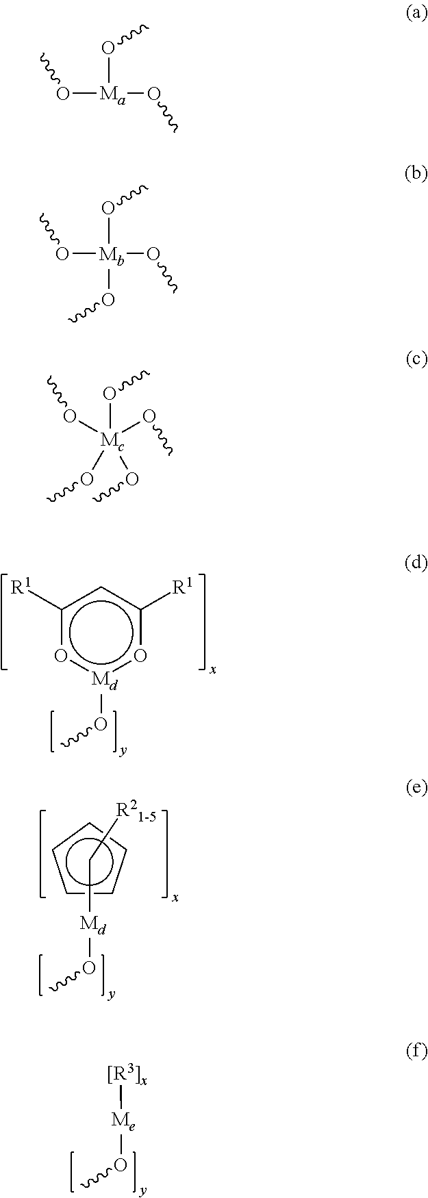
wherein x and y have the meanings above; Ma is Sc, Y, La, B, Al, Ga, In or a lanthanide metal; Mb is Ti, Zr, Hf, Ge or Sn; Mc is V, Nb, Ta, P or

Md is Ti, Zr, Hf, Sc, Y, La, a lanthanide metal, V, Nb or Ta; Mc is Ge or Sn; M′ is V or P; R1 is the same or different and is C1-C6 alkyl, C1-C6 alkoxy, phenyl or phenoxy; R2 is the same or different and is C1-C6 alkyl or C1-C6 alkoxy; R3 is the same or different and is C1-C6 alkyl or phenyl, with the proviso that Md may be another transition metal or a metal of Groups 2 to 5 of the Periodic Table.
-
- (a) providing a material layer on a substrate,
- (b) forming an antireflective hardmask composition of the invention over the material layer,
- (c) forming a radiation-sensitive imaging layer over the antireflective composition,
- (d) patternwise exposing the imaging layer to radiation thereby creating a pattern of radiation-exposed regions in the imaging layer,
- (e) selectively removing portions of the imaging layer and the antireflective hardmask composition to expose portions of the material layer, and
- (f) etching the exposed portions of the material layer, thereby forming the patterned material feature.
and Silane Precursor B was a compound having the structural formula


| TABLE 1 |
| Antireflective Hardmask Layer |
| Silane | Silane | Third Comp, | Layer | |||
| Example No. | Pre A, g | Pre B, g | g | Thick, Å | n (193 nm) | k (193 nm) |
| 1 | 0.381 | 0.069 | Ti(OC4H9)4, .549 | 2332 | 1.735 | 0.301 |
| 2 | 0.444 | 0.081 | Ge(OC2H5)4, .475 | 3073 | 1.725 | 0.294 |
| Atomic Concentration, % |
| Ex. No. | [S] | [O] | [C] | [H] | [Cl] | [Ti] | [Ge] |
| 1 | 6.1 ± 2 | 19.3 ± 2 | 30.1 ± 2 | 37.3 ± 2 | 2.9 ± 0 | 4.3 ± 0.2 | None |
| 2 | 6.1 ± 2 | 18.9 ± 2 | 27.0 ± 2 | 40.9 ± 2 | 2.9 ± 0 | None | 4.2 ± 0.2 |
Claims (18)


Priority Applications (6)
| Application Number | Priority Date | Filing Date | Title |
|---|---|---|---|
| US12/711,748 US8323871B2 (en) | 2010-02-24 | 2010-02-24 | Antireflective hardmask composition and a method of preparing a patterned material using same |
| GB1213664.4A GB2489645A (en) | 2010-02-24 | 2010-10-22 | Antireflective hardmask composition and a method of preparing a patterned material using same |
| CN201080064595.7A CN102770807B (en) | 2010-02-24 | 2010-10-22 | Antireflective hardmask composition and a method of preparing a patterned material using same |
| DE112010005304.9T DE112010005304B4 (en) | 2010-02-24 | 2010-10-22 | Antireflective hardmask composition and method of making a patterned material therewith |
| JP2012554984A JP2013522654A (en) | 2010-02-24 | 2010-10-22 | An antireflection hard mask composition and a method for preparing a patterned material using the same. |
| PCT/US2010/053652 WO2011106040A1 (en) | 2010-02-24 | 2010-10-22 | Antireflective hardmask composition and a method of preparing a patterned material using same |
Applications Claiming Priority (1)
| Application Number | Priority Date | Filing Date | Title |
|---|---|---|---|
| US12/711,748 US8323871B2 (en) | 2010-02-24 | 2010-02-24 | Antireflective hardmask composition and a method of preparing a patterned material using same |
Publications (2)
| Publication Number | Publication Date |
|---|---|
| US20110207047A1 US20110207047A1 (en) | 2011-08-25 |
| US8323871B2 true US8323871B2 (en) | 2012-12-04 |
Family
ID=44476797
Family Applications (1)
| Application Number | Title | Priority Date | Filing Date |
|---|---|---|---|
| US12/711,748 Expired - Fee Related US8323871B2 (en) | 2010-02-24 | 2010-02-24 | Antireflective hardmask composition and a method of preparing a patterned material using same |
Country Status (6)
| Country | Link |
|---|---|
| US (1) | US8323871B2 (en) |
| JP (1) | JP2013522654A (en) |
| CN (1) | CN102770807B (en) |
| DE (1) | DE112010005304B4 (en) |
| GB (1) | GB2489645A (en) |
| WO (1) | WO2011106040A1 (en) |
Cited By (1)
| Publication number | Priority date | Publication date | Assignee | Title |
|---|---|---|---|---|
| US20130011630A1 (en) * | 2011-07-07 | 2013-01-10 | Brewer Science Inc. | Metal-oxide films from small molecules for lithographic applications |
Families Citing this family (3)
| Publication number | Priority date | Publication date | Assignee | Title |
|---|---|---|---|---|
| JP5756134B2 (en) | 2013-01-08 | 2015-07-29 | 信越化学工業株式会社 | Metal oxide-containing film forming composition and pattern forming method |
| US9460934B2 (en) * | 2013-03-15 | 2016-10-04 | Globalfoundries Inc. | Wet strip process for an antireflective coating layer |
| US10007184B2 (en) * | 2016-09-01 | 2018-06-26 | Rohm And Haas Electronic Materials Llc | Silicon-containing underlayers |
Citations (47)
| Publication number | Priority date | Publication date | Assignee | Title |
|---|---|---|---|---|
| US4273420A (en) | 1978-07-07 | 1981-06-16 | Hitachi, Ltd. | Liquid crystal display device |
| JPS59175725A (en) | 1983-03-26 | 1984-10-04 | Toshiba Corp | Multilayer resist film |
| CA1204547A (en) | 1981-02-13 | 1986-05-13 | Rudolf Kirchmayr | Curable composition based on an acid-curable resin, and process for curing this resin |
| US4719146A (en) | 1984-10-27 | 1988-01-12 | Rohm Gmbh | Scratch resistant antireflective coatings for synthetic resins |
| JPH01147535A (en) | 1987-12-04 | 1989-06-09 | Koujiyundo Kagaku Kenkyusho:Kk | Multilayer resist film |
| US4855017A (en) | 1985-05-03 | 1989-08-08 | Texas Instruments Incorporated | Trench etch process for a single-wafer RIE dry etch reactor |
| JPH01293339A (en) | 1988-05-23 | 1989-11-27 | Tosoh Corp | Photoresist composition |
| US5362663A (en) | 1992-01-09 | 1994-11-08 | International Business Machines Corporation | Method of forming double well substrate plate trench DRAM cell array |
| US5429710A (en) | 1993-02-25 | 1995-07-04 | Sony Corporation | Dry etching method |
| US5562801A (en) | 1994-04-28 | 1996-10-08 | Cypress Semiconductor Corporation | Method of etching an oxide layer |
| US5580819A (en) | 1995-03-22 | 1996-12-03 | Ppg Industries, Inc. | Coating composition, process for producing antireflective coatings, and coated articles |
| US5618751A (en) | 1996-05-23 | 1997-04-08 | International Business Machines Corporation | Method of making single-step trenches using resist fill and recess |
| US5668237A (en) | 1992-06-10 | 1997-09-16 | E.I. Dupont De Nemours And Company | Silicon and zirconium based lacquer, its use as a substrate coating and substrates thus obtained |
| US5744376A (en) | 1996-04-08 | 1998-04-28 | Chartered Semiconductor Manufacturing Pte, Ltd | Method of manufacturing copper interconnect with top barrier layer |
| US5801094A (en) | 1997-02-28 | 1998-09-01 | United Microelectronics Corporation | Dual damascene process |
| US5821469A (en) | 1996-12-18 | 1998-10-13 | Lucent Technologies Inc. | Device for securing cables in a telecommunications system |
| US5886102A (en) | 1996-06-11 | 1999-03-23 | Shipley Company, L.L.C. | Antireflective coating compositions |
| US5939236A (en) | 1997-02-07 | 1999-08-17 | Shipley Company, L.L.C. | Antireflective coating compositions comprising photoacid generators |
| US5948570A (en) | 1995-05-26 | 1999-09-07 | Lucent Technologies Inc. | Process for dry lithographic etching |
| US6013582A (en) | 1997-12-08 | 2000-01-11 | Applied Materials, Inc. | Method for etching silicon oxynitride and inorganic antireflection coatings |
| US6037097A (en) | 1998-01-27 | 2000-03-14 | International Business Machines Corporation | E-beam application to mask making using new improved KRS resist system |
| US6316167B1 (en) | 2000-01-10 | 2001-11-13 | International Business Machines Corporation | Tunabale vapor deposited materials as antireflective coatings, hardmasks and as combined antireflective coating/hardmasks and methods of fabrication thereof and application thereof |
| US6420084B1 (en) | 2000-06-23 | 2002-07-16 | International Business Machines Corporation | Mask-making using resist having SIO bond-containing polymer |
| JP2003157808A (en) | 2001-11-23 | 2003-05-30 | Shogo Tsuchida | Circuit separable from reusable bulb, fluorescent lamp or the like |
| USRE38256E1 (en) | 1994-03-15 | 2003-09-23 | Kabushiki Kaisha Toshiba | Photosensitive composition |
| US20030209515A1 (en) | 1999-06-11 | 2003-11-13 | Shipley Company, L.L.C. | Antireflective hard mask compositions |
| US6669995B1 (en) | 1994-10-12 | 2003-12-30 | Linda Insalaco | Method of treating an anti-reflective coating on a substrate |
| US20040058275A1 (en) | 2002-06-25 | 2004-03-25 | Brewer Science, Inc. | Wet-developable anti-reflective compositions |
| US6730454B2 (en) | 2002-04-16 | 2004-05-04 | International Business Machines Corporation | Antireflective SiO-containing compositions for hardmask layer |
| US6743726B2 (en) | 2002-07-11 | 2004-06-01 | Promos Technologies, Inc. | Method for etching a trench through an anti-reflective coating |
| JP2004158639A (en) | 2002-11-06 | 2004-06-03 | Nec Tokin Ceramics Corp | Electric double layer capacitor |
| JP2004172222A (en) | 2002-11-18 | 2004-06-17 | Tokyo Electron Ltd | Electronic device and its manufacturing method |
| US20040253535A1 (en) | 2002-11-20 | 2004-12-16 | Shipley Company, L.L.C. | Multilayer photoresist systems |
| US20050042538A1 (en) | 2003-08-22 | 2005-02-24 | International Business Machines Corporation | Antireflective hardmask and uses thereof |
| US20050112382A1 (en) | 2003-11-24 | 2005-05-26 | Allen Robert D. | Molecular photoresists containing nonpolymeric silsesquioxanes |
| US20060014099A1 (en) | 2004-07-16 | 2006-01-19 | Faler Dennis L | Methods for producing photosensitive microparticles, aqueous compositions thereof and articles prepared therewith |
| US7011935B2 (en) | 2002-09-19 | 2006-03-14 | Arch Specialty Chemicals, Inc. | Method for the removal of an imaging layer from a semiconductor substrate stack |
| US20060093959A1 (en) | 2004-11-03 | 2006-05-04 | Huang Wu-Song S | Silicon containing TARC / barrier layer |
| US20060141390A1 (en) | 2004-12-28 | 2006-06-29 | Hynix Semiconductor Inc. | Composition for coating a photoresist pattern |
| US20060154177A1 (en) | 2003-11-17 | 2006-07-13 | Taiwan Semiconductor Manufacturing Co., Ltd. | Water soluble negative tone photoresist |
| US20070015083A1 (en) | 2005-07-14 | 2007-01-18 | International Business Machines Corporation | Antireflective composition and process of making a lithographic structure |
| US20080187731A1 (en) | 2003-09-12 | 2008-08-07 | International Business Machines Corporation | Techniques for Patterning Features in Semiconductor Devices |
| US20090029284A1 (en) | 2005-06-24 | 2009-01-29 | Tokyo Ohka Kogyo Co., Ltd. | Pattern coating material and pattern forming method |
| US20090136869A1 (en) * | 2007-11-22 | 2009-05-28 | Tsutomu Ogihara | Metal oxide-containing film-forming composition, metal oxide-containing film, metal oxide-containing film-bearing substrate, and patterning method |
| US20090176165A1 (en) | 2007-12-24 | 2009-07-09 | Cheon Hwan Sung | Polymer composition, hardmask composition having antireflective properties, and associated methods |
| US7585613B2 (en) * | 2006-01-25 | 2009-09-08 | Shin-Etsu Chemical Co., Ltd. | Antireflection film composition, substrate, and patterning process |
| US20100086872A1 (en) * | 2008-10-02 | 2010-04-08 | Shin-Etsu Chemical Co., Ltd. | Metal oxide-containing film-forming composition, metal oxide-containing film-formed substrate, and patterning process |
Family Cites Families (2)
| Publication number | Priority date | Publication date | Assignee | Title |
|---|---|---|---|---|
| US4371605A (en) | 1980-12-09 | 1983-02-01 | E. I. Du Pont De Nemours And Company | Photopolymerizable compositions containing N-hydroxyamide and N-hydroxyimide sulfonates |
| CN1253311C (en) | 2001-03-16 | 2006-04-26 | 东丽株式会社 | Laminated polyester film |
-
2010
- 2010-02-24 US US12/711,748 patent/US8323871B2/en not_active Expired - Fee Related
- 2010-10-22 DE DE112010005304.9T patent/DE112010005304B4/en active Active
- 2010-10-22 GB GB1213664.4A patent/GB2489645A/en not_active Withdrawn
- 2010-10-22 CN CN201080064595.7A patent/CN102770807B/en active Active
- 2010-10-22 WO PCT/US2010/053652 patent/WO2011106040A1/en active Application Filing
- 2010-10-22 JP JP2012554984A patent/JP2013522654A/en active Pending
Patent Citations (49)
| Publication number | Priority date | Publication date | Assignee | Title |
|---|---|---|---|---|
| US4273420A (en) | 1978-07-07 | 1981-06-16 | Hitachi, Ltd. | Liquid crystal display device |
| CA1204547A (en) | 1981-02-13 | 1986-05-13 | Rudolf Kirchmayr | Curable composition based on an acid-curable resin, and process for curing this resin |
| JPS59175725A (en) | 1983-03-26 | 1984-10-04 | Toshiba Corp | Multilayer resist film |
| US4719146A (en) | 1984-10-27 | 1988-01-12 | Rohm Gmbh | Scratch resistant antireflective coatings for synthetic resins |
| US4855017A (en) | 1985-05-03 | 1989-08-08 | Texas Instruments Incorporated | Trench etch process for a single-wafer RIE dry etch reactor |
| JPH01147535A (en) | 1987-12-04 | 1989-06-09 | Koujiyundo Kagaku Kenkyusho:Kk | Multilayer resist film |
| JPH01293339A (en) | 1988-05-23 | 1989-11-27 | Tosoh Corp | Photoresist composition |
| US5362663A (en) | 1992-01-09 | 1994-11-08 | International Business Machines Corporation | Method of forming double well substrate plate trench DRAM cell array |
| US5668237A (en) | 1992-06-10 | 1997-09-16 | E.I. Dupont De Nemours And Company | Silicon and zirconium based lacquer, its use as a substrate coating and substrates thus obtained |
| US5429710A (en) | 1993-02-25 | 1995-07-04 | Sony Corporation | Dry etching method |
| USRE38256E1 (en) | 1994-03-15 | 2003-09-23 | Kabushiki Kaisha Toshiba | Photosensitive composition |
| US5562801A (en) | 1994-04-28 | 1996-10-08 | Cypress Semiconductor Corporation | Method of etching an oxide layer |
| US6669995B1 (en) | 1994-10-12 | 2003-12-30 | Linda Insalaco | Method of treating an anti-reflective coating on a substrate |
| US5580819A (en) | 1995-03-22 | 1996-12-03 | Ppg Industries, Inc. | Coating composition, process for producing antireflective coatings, and coated articles |
| US5948570A (en) | 1995-05-26 | 1999-09-07 | Lucent Technologies Inc. | Process for dry lithographic etching |
| US5744376A (en) | 1996-04-08 | 1998-04-28 | Chartered Semiconductor Manufacturing Pte, Ltd | Method of manufacturing copper interconnect with top barrier layer |
| US5618751A (en) | 1996-05-23 | 1997-04-08 | International Business Machines Corporation | Method of making single-step trenches using resist fill and recess |
| US5886102A (en) | 1996-06-11 | 1999-03-23 | Shipley Company, L.L.C. | Antireflective coating compositions |
| US5821469A (en) | 1996-12-18 | 1998-10-13 | Lucent Technologies Inc. | Device for securing cables in a telecommunications system |
| US5939236A (en) | 1997-02-07 | 1999-08-17 | Shipley Company, L.L.C. | Antireflective coating compositions comprising photoacid generators |
| US5801094A (en) | 1997-02-28 | 1998-09-01 | United Microelectronics Corporation | Dual damascene process |
| US6013582A (en) | 1997-12-08 | 2000-01-11 | Applied Materials, Inc. | Method for etching silicon oxynitride and inorganic antireflection coatings |
| US6037097A (en) | 1998-01-27 | 2000-03-14 | International Business Machines Corporation | E-beam application to mask making using new improved KRS resist system |
| US6514667B2 (en) | 1998-06-29 | 2003-02-04 | International Business Machines Corporation | Tunable vapor deposited materials as antireflective coatings, hardmasks and as combined antireflective coating/hardmasks and methods of fabrication thereof and applications thereof |
| US20030209515A1 (en) | 1999-06-11 | 2003-11-13 | Shipley Company, L.L.C. | Antireflective hard mask compositions |
| US6316167B1 (en) | 2000-01-10 | 2001-11-13 | International Business Machines Corporation | Tunabale vapor deposited materials as antireflective coatings, hardmasks and as combined antireflective coating/hardmasks and methods of fabrication thereof and application thereof |
| US6420084B1 (en) | 2000-06-23 | 2002-07-16 | International Business Machines Corporation | Mask-making using resist having SIO bond-containing polymer |
| JP2003157808A (en) | 2001-11-23 | 2003-05-30 | Shogo Tsuchida | Circuit separable from reusable bulb, fluorescent lamp or the like |
| US6730454B2 (en) | 2002-04-16 | 2004-05-04 | International Business Machines Corporation | Antireflective SiO-containing compositions for hardmask layer |
| US20040058275A1 (en) | 2002-06-25 | 2004-03-25 | Brewer Science, Inc. | Wet-developable anti-reflective compositions |
| US6743726B2 (en) | 2002-07-11 | 2004-06-01 | Promos Technologies, Inc. | Method for etching a trench through an anti-reflective coating |
| US7011935B2 (en) | 2002-09-19 | 2006-03-14 | Arch Specialty Chemicals, Inc. | Method for the removal of an imaging layer from a semiconductor substrate stack |
| JP2004158639A (en) | 2002-11-06 | 2004-06-03 | Nec Tokin Ceramics Corp | Electric double layer capacitor |
| JP2004172222A (en) | 2002-11-18 | 2004-06-17 | Tokyo Electron Ltd | Electronic device and its manufacturing method |
| US20040253535A1 (en) | 2002-11-20 | 2004-12-16 | Shipley Company, L.L.C. | Multilayer photoresist systems |
| US20050042538A1 (en) | 2003-08-22 | 2005-02-24 | International Business Machines Corporation | Antireflective hardmask and uses thereof |
| US20080187731A1 (en) | 2003-09-12 | 2008-08-07 | International Business Machines Corporation | Techniques for Patterning Features in Semiconductor Devices |
| US20060154177A1 (en) | 2003-11-17 | 2006-07-13 | Taiwan Semiconductor Manufacturing Co., Ltd. | Water soluble negative tone photoresist |
| US20050112382A1 (en) | 2003-11-24 | 2005-05-26 | Allen Robert D. | Molecular photoresists containing nonpolymeric silsesquioxanes |
| US20060014099A1 (en) | 2004-07-16 | 2006-01-19 | Faler Dennis L | Methods for producing photosensitive microparticles, aqueous compositions thereof and articles prepared therewith |
| US20060093959A1 (en) | 2004-11-03 | 2006-05-04 | Huang Wu-Song S | Silicon containing TARC / barrier layer |
| US20060141390A1 (en) | 2004-12-28 | 2006-06-29 | Hynix Semiconductor Inc. | Composition for coating a photoresist pattern |
| US20090029284A1 (en) | 2005-06-24 | 2009-01-29 | Tokyo Ohka Kogyo Co., Ltd. | Pattern coating material and pattern forming method |
| US20070015083A1 (en) | 2005-07-14 | 2007-01-18 | International Business Machines Corporation | Antireflective composition and process of making a lithographic structure |
| US7326442B2 (en) * | 2005-07-14 | 2008-02-05 | International Business Machines Corporation | Antireflective composition and process of making a lithographic structure |
| US7585613B2 (en) * | 2006-01-25 | 2009-09-08 | Shin-Etsu Chemical Co., Ltd. | Antireflection film composition, substrate, and patterning process |
| US20090136869A1 (en) * | 2007-11-22 | 2009-05-28 | Tsutomu Ogihara | Metal oxide-containing film-forming composition, metal oxide-containing film, metal oxide-containing film-bearing substrate, and patterning method |
| US20090176165A1 (en) | 2007-12-24 | 2009-07-09 | Cheon Hwan Sung | Polymer composition, hardmask composition having antireflective properties, and associated methods |
| US20100086872A1 (en) * | 2008-10-02 | 2010-04-08 | Shin-Etsu Chemical Co., Ltd. | Metal oxide-containing film-forming composition, metal oxide-containing film-formed substrate, and patterning process |
Non-Patent Citations (1)
| Title |
|---|
| International Search Report and Written Opinion dated Feb. 28, 2011 issued in corresponding International Application No. PCT/US10/53652. |
Cited By (2)
| Publication number | Priority date | Publication date | Assignee | Title |
|---|---|---|---|---|
| US20130011630A1 (en) * | 2011-07-07 | 2013-01-10 | Brewer Science Inc. | Metal-oxide films from small molecules for lithographic applications |
| US8647809B2 (en) * | 2011-07-07 | 2014-02-11 | Brewer Science Inc. | Metal-oxide films from small molecules for lithographic applications |
Also Published As
| Publication number | Publication date |
|---|---|
| WO2011106040A1 (en) | 2011-09-01 |
| JP2013522654A (en) | 2013-06-13 |
| GB201213664D0 (en) | 2012-09-12 |
| US20110207047A1 (en) | 2011-08-25 |
| CN102770807A (en) | 2012-11-07 |
| DE112010005304T8 (en) | 2013-03-14 |
| DE112010005304B4 (en) | 2022-07-28 |
| DE112010005304T5 (en) | 2012-12-20 |
| CN102770807B (en) | 2015-05-06 |
| GB2489645A (en) | 2012-10-03 |
Similar Documents
| Publication | Publication Date | Title |
|---|---|---|
| US7223517B2 (en) | Lithographic antireflective hardmask compositions and uses thereof | |
| US7172849B2 (en) | Antireflective hardmask and uses thereof | |
| US6730454B2 (en) | Antireflective SiO-containing compositions for hardmask layer | |
| US7276327B2 (en) | Silicon-containing compositions for spin-on arc/hardmask materials | |
| US7326442B2 (en) | Antireflective composition and process of making a lithographic structure | |
| US6420088B1 (en) | Antireflective silicon-containing compositions as hardmask layer | |
| US7378217B2 (en) | Antireflective hardmask composition and methods for using same | |
| KR100816735B1 (en) | Hardmask composition having antireflective property, process of producing patterned materials by using the same and integrated circuit devices | |
| KR102367238B1 (en) | Metal hardmask composition and method of forming micropatterns on semiconductor substrates | |
| US7659051B2 (en) | Polymer having antireflective properties, hardmask composition including the same, and process for forming a patterned material layer | |
| US20130017486A1 (en) | Process of making a lithographic structure using antireflective materials | |
| EP1521797A1 (en) | Antireflective silicon-containing compositions as hardmask layer | |
| US8323871B2 (en) | Antireflective hardmask composition and a method of preparing a patterned material using same | |
| KR20070071679A (en) | Composition for hard mask and method for manufacturing semiconductor device | |
| KR20050025311A (en) | Antireflective silicon-containing compositions as hardmask layer |
Legal Events
| Date | Code | Title | Description |
|---|---|---|---|
| AS | Assignment |
Owner name: INTERNATIONAL BUSINESS MACHINES CORPORATION, NEW Y Free format text: ASSIGNMENT OF ASSIGNORS INTEREST;ASSIGNORS:BURNS, SEAN D.;MEDEIROS, DAVID R.;PFEIFFER, DIRK;SIGNING DATES FROM 20100201 TO 20100211;REEL/FRAME:023984/0787 |
|
| STCF | Information on status: patent grant |
Free format text: PATENTED CASE |
|
| AS | Assignment |
Owner name: GLOBALFOUNDRIES U.S. 2 LLC, NEW YORK Free format text: ASSIGNMENT OF ASSIGNORS INTEREST;ASSIGNOR:INTERNATIONAL BUSINESS MACHINES CORPORATION;REEL/FRAME:036550/0001 Effective date: 20150629 |
|
| AS | Assignment |
Owner name: GLOBALFOUNDRIES INC., CAYMAN ISLANDS Free format text: ASSIGNMENT OF ASSIGNORS INTEREST;ASSIGNORS:GLOBALFOUNDRIES U.S. 2 LLC;GLOBALFOUNDRIES U.S. INC.;REEL/FRAME:036779/0001 Effective date: 20150910 |
|
| FPAY | Fee payment |
Year of fee payment: 4 |
|
| AS | Assignment |
Owner name: WILMINGTON TRUST, NATIONAL ASSOCIATION, DELAWARE Free format text: SECURITY AGREEMENT;ASSIGNOR:GLOBALFOUNDRIES INC.;REEL/FRAME:049490/0001 Effective date: 20181127 |
|
| FEPP | Fee payment procedure |
Free format text: MAINTENANCE FEE REMINDER MAILED (ORIGINAL EVENT CODE: REM.); ENTITY STATUS OF PATENT OWNER: LARGE ENTITY |
|
| AS | Assignment |
Owner name: GLOBALFOUNDRIES INC., CAYMAN ISLANDS Free format text: RELEASE BY SECURED PARTY;ASSIGNOR:WILMINGTON TRUST, NATIONAL ASSOCIATION;REEL/FRAME:054636/0001 Effective date: 20201117 |
|
| LAPS | Lapse for failure to pay maintenance fees |
Free format text: PATENT EXPIRED FOR FAILURE TO PAY MAINTENANCE FEES (ORIGINAL EVENT CODE: EXP.); ENTITY STATUS OF PATENT OWNER: LARGE ENTITY |
|
| STCH | Information on status: patent discontinuation |
Free format text: PATENT EXPIRED DUE TO NONPAYMENT OF MAINTENANCE FEES UNDER 37 CFR 1.362 |
|
| FP | Lapsed due to failure to pay maintenance fee |
Effective date: 20201204 |
|
| AS | Assignment |
Owner name: GLOBALFOUNDRIES U.S. INC., NEW YORK Free format text: RELEASE BY SECURED PARTY;ASSIGNOR:WILMINGTON TRUST, NATIONAL ASSOCIATION;REEL/FRAME:056987/0001 Effective date: 20201117 |