US8329367B2 - Polyamideimide containing photoconductors - Google Patents
Polyamideimide containing photoconductors Download PDFInfo
- Publication number
- US8329367B2 US8329367B2 US12/695,420 US69542010A US8329367B2 US 8329367 B2 US8329367 B2 US 8329367B2 US 69542010 A US69542010 A US 69542010A US 8329367 B2 US8329367 B2 US 8329367B2
- Authority
- US
- United States
- Prior art keywords
- photoconductor
- charge transport
- layer
- polyamideimide
- accordance
- Prior art date
- Legal status (The legal status is an assumption and is not a legal conclusion. Google has not performed a legal analysis and makes no representation as to the accuracy of the status listed.)
- Active, expires
Links
- 239000004962 Polyamide-imide Substances 0.000 title claims abstract description 61
- 229920002312 polyamide-imide Polymers 0.000 title claims abstract description 61
- 239000000758 substrate Substances 0.000 claims abstract description 59
- 230000000903 blocking effect Effects 0.000 claims abstract description 25
- 239000010410 layer Substances 0.000 claims description 284
- -1 triethoxysilylpropylethylene diamine Chemical class 0.000 claims description 42
- 239000000049 pigment Substances 0.000 claims description 36
- IEQIEDJGQAUEQZ-UHFFFAOYSA-N phthalocyanine Chemical compound N1C(N=C2C3=CC=CC=C3C(N=C3C4=CC=CC=C4C(=N4)N3)=N2)=C(C=CC=C2)C2=C1N=C1C2=CC=CC=C2C4=N1 IEQIEDJGQAUEQZ-UHFFFAOYSA-N 0.000 claims description 27
- 239000000203 mixture Substances 0.000 claims description 26
- 239000011230 binding agent Substances 0.000 claims description 25
- 125000004432 carbon atom Chemical group C* 0.000 claims description 21
- 125000000217 alkyl group Chemical group 0.000 claims description 20
- 125000003118 aryl group Chemical group 0.000 claims description 20
- 229910052757 nitrogen Inorganic materials 0.000 claims description 20
- 239000012790 adhesive layer Substances 0.000 claims description 13
- 229920005989 resin Polymers 0.000 claims description 13
- 239000011347 resin Substances 0.000 claims description 13
- SJHHDDDGXWOYOE-UHFFFAOYSA-N oxytitamium phthalocyanine Chemical compound [Ti+2]=O.C12=CC=CC=C2C(N=C2[N-]C(C3=CC=CC=C32)=N2)=NC1=NC([C]1C=CC=CC1=1)=NC=1N=C1[C]3C=CC=CC3=C2[N-]1 SJHHDDDGXWOYOE-UHFFFAOYSA-N 0.000 claims description 11
- 125000003545 alkoxy group Chemical group 0.000 claims description 10
- 229920001296 polysiloxane Polymers 0.000 claims description 10
- FZHAPNGMFPVSLP-UHFFFAOYSA-N silanamine Chemical compound [SiH3]N FZHAPNGMFPVSLP-UHFFFAOYSA-N 0.000 claims description 8
- 239000003963 antioxidant agent Substances 0.000 claims description 6
- 229910052736 halogen Inorganic materials 0.000 claims description 6
- 150000002367 halogens Chemical class 0.000 claims description 6
- 125000002496 methyl group Chemical group [H]C([H])([H])* 0.000 claims description 6
- ZSLIEZOEYNOWCL-UHFFFAOYSA-N 4-butyl-n-[4-[4-(4-butyl-n-(4-propan-2-ylphenyl)anilino)-4-phenylcyclohexa-1,5-dien-1-yl]phenyl]-n-(4-propan-2-ylphenyl)aniline Chemical compound C1=CC(CCCC)=CC=C1N(C=1C=CC(=CC=1)C=1C=CC(CC=1)(N(C=1C=CC(CCCC)=CC=1)C=1C=CC(=CC=1)C(C)C)C=1C=CC=CC=1)C1=CC=C(C(C)C)C=C1 ZSLIEZOEYNOWCL-UHFFFAOYSA-N 0.000 claims description 5
- 230000009477 glass transition Effects 0.000 claims description 5
- PHQOGHDTIVQXHL-UHFFFAOYSA-N n'-(3-trimethoxysilylpropyl)ethane-1,2-diamine Chemical compound CO[Si](OC)(OC)CCCNCCN PHQOGHDTIVQXHL-UHFFFAOYSA-N 0.000 claims description 5
- CUHLLYPZXLBADA-UHFFFAOYSA-N n-(4-butylphenyl)-n-[4-[4-(n-(4-butylphenyl)-4-methylanilino)-4-phenylcyclohexa-1,5-dien-1-yl]phenyl]-4-methylaniline Chemical compound C1=CC(CCCC)=CC=C1N(C=1C=CC(=CC=1)C=1C=CC(CC=1)(N(C=1C=CC(C)=CC=1)C=1C=CC(CCCC)=CC=1)C=1C=CC=CC=1)C1=CC=C(C)C=C1 CUHLLYPZXLBADA-UHFFFAOYSA-N 0.000 claims description 5
- GJXJFORUMJEJPV-UHFFFAOYSA-N n-[4-[4-(4-butyl-n-(2,5-dimethylphenyl)anilino)-4-phenylcyclohexa-1,5-dien-1-yl]phenyl]-n-(4-butylphenyl)-2,5-dimethylaniline Chemical compound C1=CC(CCCC)=CC=C1N(C=1C(=CC=C(C)C=1)C)C1=CC=C(C=2C=CC(CC=2)(N(C=2C=CC(CCCC)=CC=2)C=2C(=CC=C(C)C=2)C)C=2C=CC=CC=2)C=C1 GJXJFORUMJEJPV-UHFFFAOYSA-N 0.000 claims description 5
- NCHWIKVGNQGHLZ-UHFFFAOYSA-N n-[4-[4-(4-butyl-n-(2-methylphenyl)anilino)-4-phenylcyclohexa-1,5-dien-1-yl]phenyl]-n-(4-butylphenyl)-2-methylaniline Chemical compound C1=CC(CCCC)=CC=C1N(C=1C(=CC=CC=1)C)C1=CC=C(C=2C=CC(CC=2)(N(C=2C=CC(CCCC)=CC=2)C=2C(=CC=CC=2)C)C=2C=CC=CC=2)C=C1 NCHWIKVGNQGHLZ-UHFFFAOYSA-N 0.000 claims description 5
- WYTZZXDRDKSJID-UHFFFAOYSA-N (3-aminopropyl)triethoxysilane Chemical compound CCO[Si](OCC)(OCC)CCCN WYTZZXDRDKSJID-UHFFFAOYSA-N 0.000 claims description 4
- OVFXQPOXNVQNSJ-UHFFFAOYSA-N 3-chloro-n-[4-[4-(n-(3-chlorophenyl)anilino)-4-phenylcyclohexa-1,5-dien-1-yl]phenyl]-n-phenylaniline Chemical compound ClC1=CC=CC(N(C=2C=CC=CC=2)C=2C=CC(=CC=2)C=2C=CC(CC=2)(N(C=2C=CC=CC=2)C=2C=C(Cl)C=CC=2)C=2C=CC=CC=2)=C1 OVFXQPOXNVQNSJ-UHFFFAOYSA-N 0.000 claims description 4
- NHBRUUFBSBSTHM-UHFFFAOYSA-N n'-[2-(3-trimethoxysilylpropylamino)ethyl]ethane-1,2-diamine Chemical compound CO[Si](OC)(OC)CCCNCCNCCN NHBRUUFBSBSTHM-UHFFFAOYSA-N 0.000 claims description 4
- XMJZXKUEAZLKGP-UHFFFAOYSA-N n-[4-[4-(4-butyl-n-(2-ethyl-6-methylphenyl)anilino)-4-phenylcyclohexa-1,5-dien-1-yl]phenyl]-n-(4-butylphenyl)-2-ethyl-6-methylaniline Chemical compound C1=CC(CCCC)=CC=C1N(C=1C(=CC=CC=1C)CC)C1=CC=C(C=2C=CC(CC=2)(N(C=2C=CC(CCCC)=CC=2)C=2C(=CC=CC=2C)CC)C=2C=CC=CC=2)C=C1 XMJZXKUEAZLKGP-UHFFFAOYSA-N 0.000 claims description 4
- 125000001997 phenyl group Chemical group [H]C1=C([H])C([H])=C(*)C([H])=C1[H] 0.000 claims description 4
- 125000002947 alkylene group Chemical group 0.000 claims description 3
- 150000001412 amines Chemical class 0.000 claims description 3
- SXQXVEKXOYDTRL-UHFFFAOYSA-N n-[4-[4-(4-butyl-n-(3-methylphenyl)anilino)-4-phenylcyclohexa-1,5-dien-1-yl]phenyl]-n-(4-butylphenyl)-3-methylaniline Chemical compound C1=CC(CCCC)=CC=C1N(C=1C=C(C)C=CC=1)C1=CC=C(C=2C=CC(CC=2)(N(C=2C=CC(CCCC)=CC=2)C=2C=C(C)C=CC=2)C=2C=CC=CC=2)C=C1 SXQXVEKXOYDTRL-UHFFFAOYSA-N 0.000 claims description 3
- NBXZNTLFQLUFES-UHFFFAOYSA-N triethoxy(propyl)silane Chemical compound CCC[Si](OCC)(OCC)OCC NBXZNTLFQLUFES-UHFFFAOYSA-N 0.000 claims description 3
- TXZUUQRMOIEKKQ-UHFFFAOYSA-N 2-[diethoxy(phenyl)silyl]oxy-n,n-dimethylethanamine Chemical compound CN(C)CCO[Si](OCC)(OCC)C1=CC=CC=C1 TXZUUQRMOIEKKQ-UHFFFAOYSA-N 0.000 claims description 2
- HXLAEGYMDGUSBD-UHFFFAOYSA-N 3-[diethoxy(methyl)silyl]propan-1-amine Chemical compound CCO[Si](C)(OCC)CCCN HXLAEGYMDGUSBD-UHFFFAOYSA-N 0.000 claims description 2
- SJECZPVISLOESU-UHFFFAOYSA-N 3-trimethoxysilylpropan-1-amine Chemical compound CO[Si](OC)(OC)CCCN SJECZPVISLOESU-UHFFFAOYSA-N 0.000 claims description 2
- CNODSORTHKVDEM-UHFFFAOYSA-N 4-trimethoxysilylaniline Chemical compound CO[Si](OC)(OC)C1=CC=C(N)C=C1 CNODSORTHKVDEM-UHFFFAOYSA-N 0.000 claims description 2
- 230000003078 antioxidant effect Effects 0.000 claims description 2
- 125000000031 ethylamino group Chemical group [H]C([H])([H])C([H])([H])N([H])[*] 0.000 claims description 2
- 239000001257 hydrogen Substances 0.000 claims description 2
- 229910052739 hydrogen Inorganic materials 0.000 claims description 2
- XYRLXKVOGUCZAX-UHFFFAOYSA-N n'-[3-tri(butan-2-yloxy)silylpropyl]ethane-1,2-diamine Chemical compound CCC(C)O[Si](OC(C)CC)(OC(C)CC)CCCNCCN XYRLXKVOGUCZAX-UHFFFAOYSA-N 0.000 claims description 2
- IZIQYHDAXYDQHR-UHFFFAOYSA-N n'-propyl-n'-trimethoxysilylethane-1,2-diamine Chemical compound CCCN(CCN)[Si](OC)(OC)OC IZIQYHDAXYDQHR-UHFFFAOYSA-N 0.000 claims description 2
- AQIQPUUNTCVHBS-UHFFFAOYSA-N n,n-dimethyl-3-triethoxysilylpropan-1-amine Chemical compound CCO[Si](OCC)(OCC)CCCN(C)C AQIQPUUNTCVHBS-UHFFFAOYSA-N 0.000 claims description 2
- KBJFYLLAMSZSOG-UHFFFAOYSA-N n-(3-trimethoxysilylpropyl)aniline Chemical compound CO[Si](OC)(OC)CCCNC1=CC=CC=C1 KBJFYLLAMSZSOG-UHFFFAOYSA-N 0.000 claims description 2
- DTPZJXALAREFEY-UHFFFAOYSA-N n-methyl-3-triethoxysilylpropan-1-amine Chemical compound CCO[Si](OCC)(OCC)CCCNC DTPZJXALAREFEY-UHFFFAOYSA-N 0.000 claims description 2
- ISWSIDIOOBJBQZ-UHFFFAOYSA-N phenol group Chemical group C1(=CC=CC=C1)O ISWSIDIOOBJBQZ-UHFFFAOYSA-N 0.000 claims description 2
- ZUOUZKKEUPVFJK-UHFFFAOYSA-N diphenyl Chemical compound C1=CC=CC=C1C1=CC=CC=C1 ZUOUZKKEUPVFJK-UHFFFAOYSA-N 0.000 claims 4
- 125000005428 anthryl group Chemical group [H]C1=C([H])C([H])=C2C([H])=C3C(*)=C([H])C([H])=C([H])C3=C([H])C2=C1[H] 0.000 claims 2
- 125000001797 benzyl group Chemical group [H]C1=C([H])C([H])=C(C([H])=C1[H])C([H])([H])* 0.000 claims 2
- 235000010290 biphenyl Nutrition 0.000 claims 2
- 239000004305 biphenyl Substances 0.000 claims 2
- NAJNIFLHKZVKRU-UHFFFAOYSA-N 2-methyl-n-[4-[4-(2-methylanilino)phenyl]phenyl]aniline Chemical compound CC1=CC=CC=C1NC1=CC=C(C=2C=CC(NC=3C(=CC=CC=3)C)=CC=2)C=C1 NAJNIFLHKZVKRU-UHFFFAOYSA-N 0.000 claims 1
- 241000206607 Porphyra umbilicalis Species 0.000 claims 1
- 125000004435 hydrogen atom Chemical class [H]* 0.000 claims 1
- 230000032258 transport Effects 0.000 description 123
- 238000003384 imaging method Methods 0.000 description 42
- 239000011248 coating agent Substances 0.000 description 24
- 238000000576 coating method Methods 0.000 description 24
- 238000000034 method Methods 0.000 description 23
- 239000000463 material Substances 0.000 description 22
- 229920000515 polycarbonate Polymers 0.000 description 19
- 239000004417 polycarbonate Substances 0.000 description 18
- WYURNTSHIVDZCO-UHFFFAOYSA-N Tetrahydrofuran Chemical compound C1CCOC1 WYURNTSHIVDZCO-UHFFFAOYSA-N 0.000 description 14
- 239000000243 solution Substances 0.000 description 14
- YXFVVABEGXRONW-UHFFFAOYSA-N Toluene Chemical compound CC1=CC=CC=C1 YXFVVABEGXRONW-UHFFFAOYSA-N 0.000 description 12
- 230000008569 process Effects 0.000 description 12
- 230000000052 comparative effect Effects 0.000 description 11
- 239000002904 solvent Substances 0.000 description 10
- 150000001875 compounds Chemical class 0.000 description 9
- 239000006185 dispersion Substances 0.000 description 9
- 238000001035 drying Methods 0.000 description 9
- 239000000126 substance Substances 0.000 description 9
- 229920000642 polymer Polymers 0.000 description 8
- 229910052782 aluminium Inorganic materials 0.000 description 7
- XAGFODPZIPBFFR-UHFFFAOYSA-N aluminium Chemical compound [Al] XAGFODPZIPBFFR-UHFFFAOYSA-N 0.000 description 7
- 239000004014 plasticizer Substances 0.000 description 7
- 229920001343 polytetrafluoroethylene Polymers 0.000 description 7
- 239000004810 polytetrafluoroethylene Substances 0.000 description 7
- 238000007639 printing Methods 0.000 description 7
- YLQBMQCUIZJEEH-UHFFFAOYSA-N tetrahydrofuran Natural products C=1C=COC=1 YLQBMQCUIZJEEH-UHFFFAOYSA-N 0.000 description 7
- OGGKVJMNFFSDEV-UHFFFAOYSA-N 3-methyl-n-[4-[4-(n-(3-methylphenyl)anilino)phenyl]phenyl]-n-phenylaniline Chemical compound CC1=CC=CC(N(C=2C=CC=CC=2)C=2C=CC(=CC=2)C=2C=CC(=CC=2)N(C=2C=CC=CC=2)C=2C=C(C)C=CC=2)=C1 OGGKVJMNFFSDEV-UHFFFAOYSA-N 0.000 description 6
- BVKZGUZCCUSVTD-UHFFFAOYSA-L Carbonate Chemical compound [O-]C([O-])=O BVKZGUZCCUSVTD-UHFFFAOYSA-L 0.000 description 6
- YMWUJEATGCHHMB-UHFFFAOYSA-N Dichloromethane Chemical compound ClCCl YMWUJEATGCHHMB-UHFFFAOYSA-N 0.000 description 6
- ZMXDDKWLCZADIW-UHFFFAOYSA-N N,N-Dimethylformamide Chemical compound CN(C)C=O ZMXDDKWLCZADIW-UHFFFAOYSA-N 0.000 description 6
- RTAQQCXQSZGOHL-UHFFFAOYSA-N Titanium Chemical compound [Ti] RTAQQCXQSZGOHL-UHFFFAOYSA-N 0.000 description 6
- 230000005525 hole transport Effects 0.000 description 6
- 229910052751 metal Inorganic materials 0.000 description 6
- 239000002184 metal Substances 0.000 description 6
- PRMHOXAMWFXGCO-UHFFFAOYSA-M molport-000-691-708 Chemical compound N1=C(C2=CC=CC=C2C2=NC=3C4=CC=CC=C4C(=N4)N=3)N2[Ga](Cl)N2C4=C(C=CC=C3)C3=C2N=C2C3=CC=CC=C3C1=N2 PRMHOXAMWFXGCO-UHFFFAOYSA-M 0.000 description 6
- 229920000728 polyester Polymers 0.000 description 6
- 229920002635 polyurethane Polymers 0.000 description 6
- 239000004814 polyurethane Substances 0.000 description 6
- 150000003384 small molecules Chemical class 0.000 description 6
- 239000010936 titanium Substances 0.000 description 6
- 229910052719 titanium Inorganic materials 0.000 description 6
- XLYOFNOQVPJJNP-UHFFFAOYSA-N water Substances O XLYOFNOQVPJJNP-UHFFFAOYSA-N 0.000 description 6
- 239000004952 Polyamide Substances 0.000 description 5
- 239000004793 Polystyrene Substances 0.000 description 5
- 239000002253 acid Substances 0.000 description 5
- 229920001577 copolymer Polymers 0.000 description 5
- 229920002647 polyamide Polymers 0.000 description 5
- 229920005596 polymer binder Polymers 0.000 description 5
- 239000002491 polymer binding agent Substances 0.000 description 5
- 229920002223 polystyrene Polymers 0.000 description 5
- 239000002243 precursor Substances 0.000 description 5
- 230000005855 radiation Effects 0.000 description 5
- LFQSCWFLJHTTHZ-UHFFFAOYSA-N Ethanol Chemical compound CCO LFQSCWFLJHTTHZ-UHFFFAOYSA-N 0.000 description 4
- LRHPLDYGYMQRHN-UHFFFAOYSA-N N-Butanol Chemical compound CCCCO LRHPLDYGYMQRHN-UHFFFAOYSA-N 0.000 description 4
- PXHVJJICTQNCMI-UHFFFAOYSA-N Nickel Chemical compound [Ni] PXHVJJICTQNCMI-UHFFFAOYSA-N 0.000 description 4
- 206010034972 Photosensitivity reaction Diseases 0.000 description 4
- BUGBHKTXTAQXES-UHFFFAOYSA-N Selenium Chemical compound [Se] BUGBHKTXTAQXES-UHFFFAOYSA-N 0.000 description 4
- 239000000654 additive Substances 0.000 description 4
- 230000000996 additive effect Effects 0.000 description 4
- 238000007605 air drying Methods 0.000 description 4
- 150000004982 aromatic amines Chemical class 0.000 description 4
- 230000015572 biosynthetic process Effects 0.000 description 4
- 238000006243 chemical reaction Methods 0.000 description 4
- 238000003618 dip coating Methods 0.000 description 4
- 229910052733 gallium Inorganic materials 0.000 description 4
- 230000003301 hydrolyzing effect Effects 0.000 description 4
- 239000007788 liquid Substances 0.000 description 4
- 238000000643 oven drying Methods 0.000 description 4
- 229920001568 phenolic resin Polymers 0.000 description 4
- 239000005011 phenolic resin Substances 0.000 description 4
- 230000036211 photosensitivity Effects 0.000 description 4
- 229920003207 poly(ethylene-2,6-naphthalate) Polymers 0.000 description 4
- 229920002037 poly(vinyl butyral) polymer Polymers 0.000 description 4
- 239000011112 polyethylene naphthalate Substances 0.000 description 4
- 229920000139 polyethylene terephthalate Polymers 0.000 description 4
- 239000005020 polyethylene terephthalate Substances 0.000 description 4
- 238000002360 preparation method Methods 0.000 description 4
- 229910052711 selenium Inorganic materials 0.000 description 4
- 239000011669 selenium Substances 0.000 description 4
- 239000002002 slurry Substances 0.000 description 4
- 238000005507 spraying Methods 0.000 description 4
- 238000012360 testing method Methods 0.000 description 4
- ZWEHNKRNPOVVGH-UHFFFAOYSA-N 2-Butanone Chemical compound CCC(C)=O ZWEHNKRNPOVVGH-UHFFFAOYSA-N 0.000 description 3
- QTBSBXVTEAMEQO-UHFFFAOYSA-N Acetic acid Chemical compound CC(O)=O QTBSBXVTEAMEQO-UHFFFAOYSA-N 0.000 description 3
- CSCPPACGZOOCGX-UHFFFAOYSA-N Acetone Chemical compound CC(C)=O CSCPPACGZOOCGX-UHFFFAOYSA-N 0.000 description 3
- DKPFZGUDAPQIHT-UHFFFAOYSA-N Butyl acetate Natural products CCCCOC(C)=O DKPFZGUDAPQIHT-UHFFFAOYSA-N 0.000 description 3
- RTZKZFJDLAIYFH-UHFFFAOYSA-N Diethyl ether Chemical compound CCOCC RTZKZFJDLAIYFH-UHFFFAOYSA-N 0.000 description 3
- XEKOWRVHYACXOJ-UHFFFAOYSA-N Ethyl acetate Chemical compound CCOC(C)=O XEKOWRVHYACXOJ-UHFFFAOYSA-N 0.000 description 3
- GYHNNYVSQQEPJS-UHFFFAOYSA-N Gallium Chemical compound [Ga] GYHNNYVSQQEPJS-UHFFFAOYSA-N 0.000 description 3
- OKKJLVBELUTLKV-UHFFFAOYSA-N Methanol Chemical compound OC OKKJLVBELUTLKV-UHFFFAOYSA-N 0.000 description 3
- BLRPTPMANUNPDV-UHFFFAOYSA-N Silane Chemical compound [SiH4] BLRPTPMANUNPDV-UHFFFAOYSA-N 0.000 description 3
- QCWXUUIWCKQGHC-UHFFFAOYSA-N Zirconium Chemical compound [Zr] QCWXUUIWCKQGHC-UHFFFAOYSA-N 0.000 description 3
- 230000008859 change Effects 0.000 description 3
- MVPPADPHJFYWMZ-UHFFFAOYSA-N chlorobenzene Chemical compound ClC1=CC=CC=C1 MVPPADPHJFYWMZ-UHFFFAOYSA-N 0.000 description 3
- KRKNYBCHXYNGOX-UHFFFAOYSA-N citric acid Chemical compound OC(=O)CC(O)(C(O)=O)CC(O)=O KRKNYBCHXYNGOX-UHFFFAOYSA-N 0.000 description 3
- 239000004020 conductor Substances 0.000 description 3
- 238000007796 conventional method Methods 0.000 description 3
- 239000007789 gas Substances 0.000 description 3
- 238000005227 gel permeation chromatography Methods 0.000 description 3
- PCHJSUWPFVWCPO-UHFFFAOYSA-N gold Chemical compound [Au] PCHJSUWPFVWCPO-UHFFFAOYSA-N 0.000 description 3
- 229910052737 gold Inorganic materials 0.000 description 3
- 239000010931 gold Substances 0.000 description 3
- 229920000058 polyacrylate Polymers 0.000 description 3
- 229910000077 silane Inorganic materials 0.000 description 3
- 239000011877 solvent mixture Substances 0.000 description 3
- 238000012546 transfer Methods 0.000 description 3
- 229920002554 vinyl polymer Polymers 0.000 description 3
- 229910052726 zirconium Inorganic materials 0.000 description 3
- XXWVEJFXXLLAIB-UHFFFAOYSA-N 4-[[4-(diethylamino)-2-methylphenyl]-phenylmethyl]-n,n-diethyl-3-methylaniline Chemical compound CC1=CC(N(CC)CC)=CC=C1C(C=1C(=CC(=CC=1)N(CC)CC)C)C1=CC=CC=C1 XXWVEJFXXLLAIB-UHFFFAOYSA-N 0.000 description 2
- IJGRMHOSHXDMSA-UHFFFAOYSA-N Atomic nitrogen Chemical compound N#N IJGRMHOSHXDMSA-UHFFFAOYSA-N 0.000 description 2
- 229920002799 BoPET Polymers 0.000 description 2
- 239000004322 Butylated hydroxytoluene Substances 0.000 description 2
- NLZUEZXRPGMBCV-UHFFFAOYSA-N Butylhydroxytoluene Chemical compound CC1=CC(C(C)(C)C)=C(O)C(C(C)(C)C)=C1 NLZUEZXRPGMBCV-UHFFFAOYSA-N 0.000 description 2
- OKTJSMMVPCPJKN-UHFFFAOYSA-N Carbon Chemical compound [C] OKTJSMMVPCPJKN-UHFFFAOYSA-N 0.000 description 2
- HEDRZPFGACZZDS-UHFFFAOYSA-N Chloroform Chemical compound ClC(Cl)Cl HEDRZPFGACZZDS-UHFFFAOYSA-N 0.000 description 2
- CTQNGGLPUBDAKN-UHFFFAOYSA-N O-Xylene Chemical compound CC1=CC=CC=C1C CTQNGGLPUBDAKN-UHFFFAOYSA-N 0.000 description 2
- NBIIXXVUZAFLBC-UHFFFAOYSA-N Phosphoric acid Chemical compound OP(O)(O)=O NBIIXXVUZAFLBC-UHFFFAOYSA-N 0.000 description 2
- 239000004642 Polyimide Substances 0.000 description 2
- 229910001370 Se alloy Inorganic materials 0.000 description 2
- KKEYFWRCBNTPAC-UHFFFAOYSA-N Terephthalic acid Chemical compound OC(=O)C1=CC=C(C(O)=O)C=C1 KKEYFWRCBNTPAC-UHFFFAOYSA-N 0.000 description 2
- GWEVSGVZZGPLCZ-UHFFFAOYSA-N Titan oxide Chemical compound O=[Ti]=O GWEVSGVZZGPLCZ-UHFFFAOYSA-N 0.000 description 2
- BZHJMEDXRYGGRV-UHFFFAOYSA-N Vinyl chloride Chemical compound ClC=C BZHJMEDXRYGGRV-UHFFFAOYSA-N 0.000 description 2
- XLOMVQKBTHCTTD-UHFFFAOYSA-N Zinc monoxide Chemical compound [Zn]=O XLOMVQKBTHCTTD-UHFFFAOYSA-N 0.000 description 2
- BGYHLZZASRKEJE-UHFFFAOYSA-N [3-[3-(3,5-ditert-butyl-4-hydroxyphenyl)propanoyloxy]-2,2-bis[3-(3,5-ditert-butyl-4-hydroxyphenyl)propanoyloxymethyl]propyl] 3-(3,5-ditert-butyl-4-hydroxyphenyl)propanoate Chemical compound CC(C)(C)C1=C(O)C(C(C)(C)C)=CC(CCC(=O)OCC(COC(=O)CCC=2C=C(C(O)=C(C=2)C(C)(C)C)C(C)(C)C)(COC(=O)CCC=2C=C(C(O)=C(C=2)C(C)(C)C)C(C)(C)C)COC(=O)CCC=2C=C(C(O)=C(C=2)C(C)(C)C)C(C)(C)C)=C1 BGYHLZZASRKEJE-UHFFFAOYSA-N 0.000 description 2
- 230000002411 adverse Effects 0.000 description 2
- 229920000180 alkyd Polymers 0.000 description 2
- 229920005603 alternating copolymer Polymers 0.000 description 2
- 150000001408 amides Chemical class 0.000 description 2
- 238000004458 analytical method Methods 0.000 description 2
- 239000012736 aqueous medium Substances 0.000 description 2
- 239000011324 bead Substances 0.000 description 2
- 230000008901 benefit Effects 0.000 description 2
- 125000000484 butyl group Chemical group [H]C([*])([H])C([H])([H])C([H])([H])C([H])([H])[H] 0.000 description 2
- 235000010354 butylated hydroxytoluene Nutrition 0.000 description 2
- 229940095259 butylated hydroxytoluene Drugs 0.000 description 2
- 229910052799 carbon Inorganic materials 0.000 description 2
- 239000000460 chlorine Substances 0.000 description 2
- 229910052801 chlorine Inorganic materials 0.000 description 2
- 125000004122 cyclic group Chemical group 0.000 description 2
- JHIVVAPYMSGYDF-UHFFFAOYSA-N cyclohexanone Chemical compound O=C1CCCCC1 JHIVVAPYMSGYDF-UHFFFAOYSA-N 0.000 description 2
- 230000007547 defect Effects 0.000 description 2
- 230000001419 dependent effect Effects 0.000 description 2
- 125000001495 ethyl group Chemical group [H]C([H])([H])C([H])([H])* 0.000 description 2
- 229910052732 germanium Inorganic materials 0.000 description 2
- GNPVGFCGXDBREM-UHFFFAOYSA-N germanium atom Chemical compound [Ge] GNPVGFCGXDBREM-UHFFFAOYSA-N 0.000 description 2
- 150000007857 hydrazones Chemical class 0.000 description 2
- XMBWDFGMSWQBCA-UHFFFAOYSA-N hydrogen iodide Chemical compound I XMBWDFGMSWQBCA-UHFFFAOYSA-N 0.000 description 2
- 238000010348 incorporation Methods 0.000 description 2
- 238000002347 injection Methods 0.000 description 2
- 239000007924 injection Substances 0.000 description 2
- 150000002500 ions Chemical class 0.000 description 2
- 239000012948 isocyanate Substances 0.000 description 2
- 150000002513 isocyanates Chemical class 0.000 description 2
- 229910044991 metal oxide Inorganic materials 0.000 description 2
- 150000004706 metal oxides Chemical class 0.000 description 2
- BDAGIHXWWSANSR-UHFFFAOYSA-N methanoic acid Natural products OC=O BDAGIHXWWSANSR-UHFFFAOYSA-N 0.000 description 2
- 230000005012 migration Effects 0.000 description 2
- 238000013508 migration Methods 0.000 description 2
- 150000007522 mineralic acids Chemical class 0.000 description 2
- 238000002156 mixing Methods 0.000 description 2
- 229910052759 nickel Inorganic materials 0.000 description 2
- 230000003287 optical effect Effects 0.000 description 2
- 150000007524 organic acids Chemical class 0.000 description 2
- 239000002245 particle Substances 0.000 description 2
- 125000002080 perylenyl group Chemical class C1(=CC=C2C=CC=C3C4=CC=CC5=CC=CC(C1=C23)=C45)* 0.000 description 2
- 239000002530 phenolic antioxidant Substances 0.000 description 2
- 150000002989 phenols Chemical class 0.000 description 2
- 229920003227 poly(N-vinyl carbazole) Polymers 0.000 description 2
- 229920002239 polyacrylonitrile Polymers 0.000 description 2
- 229920000647 polyepoxide Polymers 0.000 description 2
- 229920001721 polyimide Polymers 0.000 description 2
- 229920002451 polyvinyl alcohol Polymers 0.000 description 2
- 229920000915 polyvinyl chloride Polymers 0.000 description 2
- 239000004800 polyvinyl chloride Substances 0.000 description 2
- 125000001436 propyl group Chemical group [H]C([*])([H])C([H])([H])C([H])([H])[H] 0.000 description 2
- 229920005604 random copolymer Polymers 0.000 description 2
- 239000007787 solid Substances 0.000 description 2
- VZGDMQKNWNREIO-UHFFFAOYSA-N tetrachloromethane Chemical compound ClC(Cl)(Cl)Cl VZGDMQKNWNREIO-UHFFFAOYSA-N 0.000 description 2
- JOXIMZWYDAKGHI-UHFFFAOYSA-N toluene-4-sulfonic acid Chemical compound CC1=CC=C(S(O)(=O)=O)C=C1 JOXIMZWYDAKGHI-UHFFFAOYSA-N 0.000 description 2
- 238000005406 washing Methods 0.000 description 2
- 239000008096 xylene Substances 0.000 description 2
- YOBOXHGSEJBUPB-MTOQALJVSA-N (z)-4-hydroxypent-3-en-2-one;zirconium Chemical compound [Zr].C\C(O)=C\C(C)=O.C\C(O)=C\C(C)=O.C\C(O)=C\C(C)=O.C\C(O)=C\C(C)=O YOBOXHGSEJBUPB-MTOQALJVSA-N 0.000 description 1
- RYHBNJHYFVUHQT-UHFFFAOYSA-N 1,4-Dioxane Chemical compound C1COCCO1 RYHBNJHYFVUHQT-UHFFFAOYSA-N 0.000 description 1
- XJKSTNDFUHDPQJ-UHFFFAOYSA-N 1,4-diphenylbenzene Chemical group C1=CC=CC=C1C1=CC=C(C=2C=CC=CC=2)C=C1 XJKSTNDFUHDPQJ-UHFFFAOYSA-N 0.000 description 1
- DIQZGCCQHMIOLR-UHFFFAOYSA-N 2-[(3,5-ditert-butyl-4-hydroxyphenyl)methyl]prop-2-enoic acid;methane Chemical compound C.CC(C)(C)C1=CC(CC(=C)C(O)=O)=CC(C(C)(C)C)=C1O DIQZGCCQHMIOLR-UHFFFAOYSA-N 0.000 description 1
- NGNBDVOYPDDBFK-UHFFFAOYSA-N 2-[2,4-di(pentan-2-yl)phenoxy]acetyl chloride Chemical compound CCCC(C)C1=CC=C(OCC(Cl)=O)C(C(C)CCC)=C1 NGNBDVOYPDDBFK-UHFFFAOYSA-N 0.000 description 1
- KXGFMDJXCMQABM-UHFFFAOYSA-N 2-methoxy-6-methylphenol Chemical compound [CH]OC1=CC=CC([CH])=C1O KXGFMDJXCMQABM-UHFFFAOYSA-N 0.000 description 1
- XLLIQLLCWZCATF-UHFFFAOYSA-N 2-methoxyethyl acetate Chemical compound COCCOC(C)=O XLLIQLLCWZCATF-UHFFFAOYSA-N 0.000 description 1
- SSADPHQCUURWSW-UHFFFAOYSA-N 3,9-bis(2,6-ditert-butyl-4-methylphenoxy)-2,4,8,10-tetraoxa-3,9-diphosphaspiro[5.5]undecane Chemical compound CC(C)(C)C1=CC(C)=CC(C(C)(C)C)=C1OP1OCC2(COP(OC=3C(=CC(C)=CC=3C(C)(C)C)C(C)(C)C)OC2)CO1 SSADPHQCUURWSW-UHFFFAOYSA-N 0.000 description 1
- OSWFIVFLDKOXQC-UHFFFAOYSA-N 4-(3-methoxyphenyl)aniline Chemical compound COC1=CC=CC(C=2C=CC(N)=CC=2)=C1 OSWFIVFLDKOXQC-UHFFFAOYSA-N 0.000 description 1
- XJCZPEXSCKWWRX-UHFFFAOYSA-N 4-[4-(4-butyl-n-(3-methylphenyl)anilino)phenyl]-n-(4-butylphenyl)-n-(3-methylphenyl)-3-phenylaniline Chemical compound C1=CC(CCCC)=CC=C1N(C=1C=C(C)C=CC=1)C1=CC=C(C=2C(=CC(=CC=2)N(C=2C=CC(CCCC)=CC=2)C=2C=C(C)C=CC=2)C=2C=CC=CC=2)C=C1 XJCZPEXSCKWWRX-UHFFFAOYSA-N 0.000 description 1
- XGBDLEXVEKHYBY-UHFFFAOYSA-N 4-benzhydrylbenzene-1,2,3-triamine Chemical compound NC1=C(C(=C(C=C1)C(C1=CC=CC=C1)C1=CC=CC=C1)N)N XGBDLEXVEKHYBY-UHFFFAOYSA-N 0.000 description 1
- HCTHYIRJERPQJA-UHFFFAOYSA-N 7,14,25,32-tetrazaundecacyclo[21.13.2.22,5.03,19.04,16.06,14.08,13.020,37.025,33.026,31.034,38]tetraconta-1(37),2,4,6,8,10,12,16,18,20,22,26,28,30,32,34(38),35,39-octadecaene-15,24-dione Chemical group C1=CC=C2N(C(C3=CC=C4C5=CC=C6C(N7C8=CC=CC=C8N=C7C7=CC=C(C5=C67)C=5C=CC6=C3C4=5)=O)=O)C6=NC2=C1 HCTHYIRJERPQJA-UHFFFAOYSA-N 0.000 description 1
- OMIHGPLIXGGMJB-UHFFFAOYSA-N 7-oxabicyclo[4.1.0]hepta-1,3,5-triene Chemical compound C1=CC=C2OC2=C1 OMIHGPLIXGGMJB-UHFFFAOYSA-N 0.000 description 1
- 229910000967 As alloy Inorganic materials 0.000 description 1
- 229910001369 Brass Inorganic materials 0.000 description 1
- CPELXLSAUQHCOX-UHFFFAOYSA-M Bromide Chemical compound [Br-] CPELXLSAUQHCOX-UHFFFAOYSA-M 0.000 description 1
- 239000004215 Carbon black (E152) Substances 0.000 description 1
- VEXZGXHMUGYJMC-UHFFFAOYSA-M Chloride anion Chemical compound [Cl-] VEXZGXHMUGYJMC-UHFFFAOYSA-M 0.000 description 1
- ZAMOUSCENKQFHK-UHFFFAOYSA-N Chlorine atom Chemical compound [Cl] ZAMOUSCENKQFHK-UHFFFAOYSA-N 0.000 description 1
- VYZAMTAEIAYCRO-UHFFFAOYSA-N Chromium Chemical compound [Cr] VYZAMTAEIAYCRO-UHFFFAOYSA-N 0.000 description 1
- 229920001634 Copolyester Polymers 0.000 description 1
- RYGMFSIKBFXOCR-UHFFFAOYSA-N Copper Chemical compound [Cu] RYGMFSIKBFXOCR-UHFFFAOYSA-N 0.000 description 1
- MQIUGAXCHLFZKX-UHFFFAOYSA-N Di-n-octyl phthalate Natural products CCCCCCCCOC(=O)C1=CC=CC=C1C(=O)OCCCCCCCC MQIUGAXCHLFZKX-UHFFFAOYSA-N 0.000 description 1
- 239000004641 Diallyl-phthalate Substances 0.000 description 1
- 239000004593 Epoxy Substances 0.000 description 1
- 239000005977 Ethylene Substances 0.000 description 1
- KRHYYFGTRYWZRS-UHFFFAOYSA-M Fluoride anion Chemical compound [F-] KRHYYFGTRYWZRS-UHFFFAOYSA-M 0.000 description 1
- UFHFLCQGNIYNRP-UHFFFAOYSA-N Hydrogen Chemical compound [H][H] UFHFLCQGNIYNRP-UHFFFAOYSA-N 0.000 description 1
- 239000004425 Makrolon Substances 0.000 description 1
- FXHOOIRPVKKKFG-UHFFFAOYSA-N N,N-Dimethylacetamide Chemical compound CN(C)C(C)=O FXHOOIRPVKKKFG-UHFFFAOYSA-N 0.000 description 1
- SECXISVLQFMRJM-UHFFFAOYSA-N N-Methylpyrrolidone Chemical compound CN1CCCC1=O SECXISVLQFMRJM-UHFFFAOYSA-N 0.000 description 1
- AMQJEAYHLZJPGS-UHFFFAOYSA-N N-Pentanol Chemical compound CCCCCO AMQJEAYHLZJPGS-UHFFFAOYSA-N 0.000 description 1
- 206010067482 No adverse event Diseases 0.000 description 1
- 239000004677 Nylon Substances 0.000 description 1
- 239000004698 Polyethylene Substances 0.000 description 1
- 239000004743 Polypropylene Substances 0.000 description 1
- 229910052581 Si3N4 Inorganic materials 0.000 description 1
- XUIMIQQOPSSXEZ-UHFFFAOYSA-N Silicon Chemical compound [Si] XUIMIQQOPSSXEZ-UHFFFAOYSA-N 0.000 description 1
- 229910000831 Steel Inorganic materials 0.000 description 1
- XSTXAVWGXDQKEL-UHFFFAOYSA-N Trichloroethylene Chemical group ClC=C(Cl)Cl XSTXAVWGXDQKEL-UHFFFAOYSA-N 0.000 description 1
- XTXRWKRVRITETP-UHFFFAOYSA-N Vinyl acetate Chemical compound CC(=O)OC=C XTXRWKRVRITETP-UHFFFAOYSA-N 0.000 description 1
- 229920001986 Vinylidene chloride-vinyl chloride copolymer Polymers 0.000 description 1
- 235000010724 Wisteria floribunda Nutrition 0.000 description 1
- 238000005299 abrasion Methods 0.000 description 1
- 150000001241 acetals Chemical class 0.000 description 1
- 150000001298 alcohols Chemical class 0.000 description 1
- 150000001338 aliphatic hydrocarbons Chemical class 0.000 description 1
- 150000004703 alkoxides Chemical class 0.000 description 1
- 229910045601 alloy Inorganic materials 0.000 description 1
- 239000000956 alloy Substances 0.000 description 1
- 229910000147 aluminium phosphate Inorganic materials 0.000 description 1
- 229920003180 amino resin Polymers 0.000 description 1
- 229910021417 amorphous silicon Inorganic materials 0.000 description 1
- 150000004945 aromatic hydrocarbons Chemical class 0.000 description 1
- RQNWIZPPADIBDY-UHFFFAOYSA-N arsenic atom Chemical compound [As] RQNWIZPPADIBDY-UHFFFAOYSA-N 0.000 description 1
- QVGXLLKOCUKJST-UHFFFAOYSA-N atomic oxygen Chemical compound [O] QVGXLLKOCUKJST-UHFFFAOYSA-N 0.000 description 1
- 238000010533 azeotropic distillation Methods 0.000 description 1
- 238000000498 ball milling Methods 0.000 description 1
- IFVTZJHWGZSXFD-UHFFFAOYSA-N biphenylene Chemical group C1=CC=C2C3=CC=CC=C3C2=C1 IFVTZJHWGZSXFD-UHFFFAOYSA-N 0.000 description 1
- BJQHLKABXJIVAM-UHFFFAOYSA-N bis(2-ethylhexyl) phthalate Chemical compound CCCCC(CC)COC(=O)C1=CC=CC=C1C(=O)OCC(CC)CCCC BJQHLKABXJIVAM-UHFFFAOYSA-N 0.000 description 1
- TUOSWEIWIXJUAU-UHFFFAOYSA-N bis(7-methyloctyl) cyclohexane-1,1-dicarboxylate Chemical compound CC(C)CCCCCCOC(=O)C1(C(=O)OCCCCCCC(C)C)CCCCC1 TUOSWEIWIXJUAU-UHFFFAOYSA-N 0.000 description 1
- QUDWYFHPNIMBFC-UHFFFAOYSA-N bis(prop-2-enyl) benzene-1,2-dicarboxylate Chemical compound C=CCOC(=O)C1=CC=CC=C1C(=O)OCC=C QUDWYFHPNIMBFC-UHFFFAOYSA-N 0.000 description 1
- 229920000402 bisphenol A polycarbonate polymer Polymers 0.000 description 1
- 229920001400 block copolymer Polymers 0.000 description 1
- 238000009835 boiling Methods 0.000 description 1
- 239000005388 borosilicate glass Substances 0.000 description 1
- 239000010951 brass Substances 0.000 description 1
- 239000006229 carbon black Substances 0.000 description 1
- 229920002678 cellulose Polymers 0.000 description 1
- 239000001913 cellulose Substances 0.000 description 1
- 238000007600 charging Methods 0.000 description 1
- 125000001309 chloro group Chemical group Cl* 0.000 description 1
- XOYLJNJLGBYDTH-UHFFFAOYSA-M chlorogallium Chemical compound [Ga]Cl XOYLJNJLGBYDTH-UHFFFAOYSA-M 0.000 description 1
- 229910052804 chromium Inorganic materials 0.000 description 1
- 239000011651 chromium Substances 0.000 description 1
- 239000011247 coating layer Substances 0.000 description 1
- 239000003086 colorant Substances 0.000 description 1
- 238000010280 constant potential charging Methods 0.000 description 1
- 229910052802 copper Inorganic materials 0.000 description 1
- 239000010949 copper Substances 0.000 description 1
- 230000001351 cycling effect Effects 0.000 description 1
- QYQADNCHXSEGJT-UHFFFAOYSA-N cyclohexane-1,1-dicarboxylate;hydron Chemical compound OC(=O)C1(C(O)=O)CCCCC1 QYQADNCHXSEGJT-UHFFFAOYSA-N 0.000 description 1
- 230000003247 decreasing effect Effects 0.000 description 1
- 230000002950 deficient Effects 0.000 description 1
- 230000008021 deposition Effects 0.000 description 1
- 238000011161 development Methods 0.000 description 1
- 150000004985 diamines Chemical class 0.000 description 1
- 238000000113 differential scanning calorimetry Methods 0.000 description 1
- 239000000539 dimer Substances 0.000 description 1
- 229940113088 dimethylacetamide Drugs 0.000 description 1
- 239000002270 dispersing agent Substances 0.000 description 1
- 239000012799 electrically-conductive coating Substances 0.000 description 1
- 230000008030 elimination Effects 0.000 description 1
- 238000003379 elimination reaction Methods 0.000 description 1
- 238000005516 engineering process Methods 0.000 description 1
- 125000003700 epoxy group Chemical group 0.000 description 1
- 239000003822 epoxy resin Substances 0.000 description 1
- 150000002148 esters Chemical class 0.000 description 1
- 150000002170 ethers Chemical class 0.000 description 1
- 238000001125 extrusion Methods 0.000 description 1
- 239000004744 fabric Substances 0.000 description 1
- 235000019253 formic acid Nutrition 0.000 description 1
- UPWPDUACHOATKO-UHFFFAOYSA-K gallium trichloride Chemical compound Cl[Ga](Cl)Cl UPWPDUACHOATKO-UHFFFAOYSA-K 0.000 description 1
- 239000011521 glass Substances 0.000 description 1
- 238000007756 gravure coating Methods 0.000 description 1
- LNEPOXFFQSENCJ-UHFFFAOYSA-N haloperidol Chemical compound C1CC(O)(C=2C=CC(Cl)=CC=2)CCN1CCCC(=O)C1=CC=C(F)C=C1 LNEPOXFFQSENCJ-UHFFFAOYSA-N 0.000 description 1
- FUZZWVXGSFPDMH-UHFFFAOYSA-M hexanoate Chemical compound CCCCCC([O-])=O FUZZWVXGSFPDMH-UHFFFAOYSA-M 0.000 description 1
- 125000004051 hexyl group Chemical group [H]C([H])([H])C([H])([H])C([H])([H])C([H])([H])C([H])([H])C([H])([H])* 0.000 description 1
- 238000010316 high energy milling Methods 0.000 description 1
- 229930195733 hydrocarbon Natural products 0.000 description 1
- 150000002430 hydrocarbons Chemical class 0.000 description 1
- 229910000043 hydrogen iodide Inorganic materials 0.000 description 1
- 230000007062 hydrolysis Effects 0.000 description 1
- 238000006460 hydrolysis reaction Methods 0.000 description 1
- 125000002887 hydroxy group Chemical group [H]O* 0.000 description 1
- 238000005286 illumination Methods 0.000 description 1
- 150000003949 imides Chemical class 0.000 description 1
- 238000010952 in-situ formation Methods 0.000 description 1
- AMGQUBHHOARCQH-UHFFFAOYSA-N indium;oxotin Chemical compound [In].[Sn]=O AMGQUBHHOARCQH-UHFFFAOYSA-N 0.000 description 1
- 229910010272 inorganic material Inorganic materials 0.000 description 1
- 239000011147 inorganic material Substances 0.000 description 1
- 239000001023 inorganic pigment Substances 0.000 description 1
- 239000011810 insulating material Substances 0.000 description 1
- 239000012212 insulator Substances 0.000 description 1
- 150000002576 ketones Chemical class 0.000 description 1
- 230000014759 maintenance of location Effects 0.000 description 1
- 238000004519 manufacturing process Methods 0.000 description 1
- 239000011159 matrix material Substances 0.000 description 1
- 239000002609 medium Substances 0.000 description 1
- 150000002734 metacrylic acid derivatives Chemical class 0.000 description 1
- 239000011859 microparticle Substances 0.000 description 1
- 238000012986 modification Methods 0.000 description 1
- 230000004048 modification Effects 0.000 description 1
- 239000000178 monomer Substances 0.000 description 1
- SCYKZELSWZRBIM-UHFFFAOYSA-N n-(3-chlorophenyl)-4-[4-(n-(3-chlorophenyl)anilino)phenyl]-n,3-diphenylaniline Chemical compound ClC1=CC=CC(N(C=2C=CC=CC=2)C=2C=CC(=CC=2)C=2C(=CC(=CC=2)N(C=2C=CC=CC=2)C=2C=C(Cl)C=CC=2)C=2C=CC=CC=2)=C1 SCYKZELSWZRBIM-UHFFFAOYSA-N 0.000 description 1
- 230000007935 neutral effect Effects 0.000 description 1
- 239000012811 non-conductive material Substances 0.000 description 1
- 229920001778 nylon Polymers 0.000 description 1
- 239000011368 organic material Substances 0.000 description 1
- 239000012860 organic pigment Substances 0.000 description 1
- 239000003960 organic solvent Substances 0.000 description 1
- 150000004866 oxadiazoles Chemical class 0.000 description 1
- 229910052760 oxygen Inorganic materials 0.000 description 1
- 239000001301 oxygen Substances 0.000 description 1
- 229930184652 p-Terphenyl Natural products 0.000 description 1
- NFHFRUOZVGFOOS-UHFFFAOYSA-N palladium;triphenylphosphane Chemical compound [Pd].C1=CC=CC=C1P(C=1C=CC=CC=1)C1=CC=CC=C1.C1=CC=CC=C1P(C=1C=CC=CC=1)C1=CC=CC=C1.C1=CC=CC=C1P(C=1C=CC=CC=1)C1=CC=CC=C1.C1=CC=CC=C1P(C=1C=CC=CC=1)C1=CC=CC=C1 NFHFRUOZVGFOOS-UHFFFAOYSA-N 0.000 description 1
- 125000001147 pentyl group Chemical group C(CCCC)* 0.000 description 1
- CSHWQDPOILHKBI-UHFFFAOYSA-N peryrene Natural products C1=CC(C2=CC=CC=3C2=C2C=CC=3)=C3C2=CC=CC3=C1 CSHWQDPOILHKBI-UHFFFAOYSA-N 0.000 description 1
- 229920006287 phenoxy resin Polymers 0.000 description 1
- 239000013034 phenoxy resin Substances 0.000 description 1
- OJMIONKXNSYLSR-UHFFFAOYSA-N phosphorous acid Chemical compound OP(O)O OJMIONKXNSYLSR-UHFFFAOYSA-N 0.000 description 1
- 108091008695 photoreceptors Proteins 0.000 description 1
- XNGIFLGASWRNHJ-UHFFFAOYSA-L phthalate(2-) Chemical compound [O-]C(=O)C1=CC=CC=C1C([O-])=O XNGIFLGASWRNHJ-UHFFFAOYSA-L 0.000 description 1
- 229920000090 poly(aryl ether) Polymers 0.000 description 1
- 229920002492 poly(sulfone) Polymers 0.000 description 1
- 229920001230 polyarylate Polymers 0.000 description 1
- 229920002857 polybutadiene Polymers 0.000 description 1
- 229920005668 polycarbonate resin Polymers 0.000 description 1
- 239000004431 polycarbonate resin Substances 0.000 description 1
- 125000003367 polycyclic group Chemical group 0.000 description 1
- 229920006393 polyether sulfone Polymers 0.000 description 1
- 229920000573 polyethylene Polymers 0.000 description 1
- 229920000306 polymethylpentene Polymers 0.000 description 1
- 229920001155 polypropylene Polymers 0.000 description 1
- 229920002689 polyvinyl acetate Polymers 0.000 description 1
- 239000011118 polyvinyl acetate Substances 0.000 description 1
- 229920002717 polyvinylpyridine Polymers 0.000 description 1
- 239000000843 powder Substances 0.000 description 1
- 230000001376 precipitating effect Effects 0.000 description 1
- DNXIASIHZYFFRO-UHFFFAOYSA-N pyrazoline Chemical compound C1CN=NC1 DNXIASIHZYFFRO-UHFFFAOYSA-N 0.000 description 1
- 150000003219 pyrazolines Chemical class 0.000 description 1
- 230000001105 regulatory effect Effects 0.000 description 1
- 230000035945 sensitivity Effects 0.000 description 1
- 229910052710 silicon Inorganic materials 0.000 description 1
- 239000010703 silicon Substances 0.000 description 1
- HQVNEWCFYHHQES-UHFFFAOYSA-N silicon nitride Chemical compound N12[Si]34N5[Si]62N3[Si]51N64 HQVNEWCFYHHQES-UHFFFAOYSA-N 0.000 description 1
- 238000004088 simulation Methods 0.000 description 1
- 239000006104 solid solution Substances 0.000 description 1
- 239000007921 spray Substances 0.000 description 1
- 238000010561 standard procedure Methods 0.000 description 1
- 239000010959 steel Substances 0.000 description 1
- 150000001629 stilbenes Chemical class 0.000 description 1
- 235000021286 stilbenes Nutrition 0.000 description 1
- 229920003048 styrene butadiene rubber Polymers 0.000 description 1
- 150000003440 styrenes Chemical class 0.000 description 1
- 125000001424 substituent group Chemical group 0.000 description 1
- 125000000547 substituted alkyl group Chemical group 0.000 description 1
- 229940124530 sulfonamide Drugs 0.000 description 1
- 150000003456 sulfonamides Chemical class 0.000 description 1
- 239000002344 surface layer Substances 0.000 description 1
- 229910052714 tellurium Inorganic materials 0.000 description 1
- PORWMNRCUJJQNO-UHFFFAOYSA-N tellurium atom Chemical compound [Te] PORWMNRCUJJQNO-UHFFFAOYSA-N 0.000 description 1
- 229920001169 thermoplastic Polymers 0.000 description 1
- 229920005992 thermoplastic resin Polymers 0.000 description 1
- 229920001187 thermosetting polymer Polymers 0.000 description 1
- 239000004416 thermosoftening plastic Substances 0.000 description 1
- 150000003568 thioethers Chemical class 0.000 description 1
- 239000004408 titanium dioxide Substances 0.000 description 1
- UBOXGVDOUJQMTN-UHFFFAOYSA-N trichloroethylene Natural products ClCC(Cl)Cl UBOXGVDOUJQMTN-UHFFFAOYSA-N 0.000 description 1
- SRPWOOOHEPICQU-UHFFFAOYSA-N trimellitic anhydride Chemical compound OC(=O)C1=CC=C2C(=O)OC(=O)C2=C1 SRPWOOOHEPICQU-UHFFFAOYSA-N 0.000 description 1
- NJMOHBDCGXJLNJ-UHFFFAOYSA-N trimellitic anhydride chloride Chemical compound ClC(=O)C1=CC=C2C(=O)OC(=O)C2=C1 NJMOHBDCGXJLNJ-UHFFFAOYSA-N 0.000 description 1
- 238000001771 vacuum deposition Methods 0.000 description 1
- 238000007738 vacuum evaporation Methods 0.000 description 1
- 238000002061 vacuum sublimation Methods 0.000 description 1
- 125000005287 vanadyl group Chemical group 0.000 description 1
- 229920006163 vinyl copolymer Polymers 0.000 description 1
- 125000000391 vinyl group Chemical group [H]C([*])=C([H])[H] 0.000 description 1
- 239000011787 zinc oxide Substances 0.000 description 1
Classifications
-
- G—PHYSICS
- G03—PHOTOGRAPHY; CINEMATOGRAPHY; ANALOGOUS TECHNIQUES USING WAVES OTHER THAN OPTICAL WAVES; ELECTROGRAPHY; HOLOGRAPHY
- G03G—ELECTROGRAPHY; ELECTROPHOTOGRAPHY; MAGNETOGRAPHY
- G03G5/00—Recording members for original recording by exposure, e.g. to light, to heat, to electrons; Manufacture thereof; Selection of materials therefor
- G03G5/02—Charge-receiving layers
- G03G5/04—Photoconductive layers; Charge-generation layers or charge-transporting layers; Additives therefor; Binders therefor
- G03G5/05—Organic bonding materials; Methods for coating a substrate with a photoconductive layer; Inert supplements for use in photoconductive layers
- G03G5/0528—Macromolecular bonding materials
- G03G5/0596—Macromolecular compounds characterised by their physical properties
-
- G—PHYSICS
- G03—PHOTOGRAPHY; CINEMATOGRAPHY; ANALOGOUS TECHNIQUES USING WAVES OTHER THAN OPTICAL WAVES; ELECTROGRAPHY; HOLOGRAPHY
- G03G—ELECTROGRAPHY; ELECTROPHOTOGRAPHY; MAGNETOGRAPHY
- G03G5/00—Recording members for original recording by exposure, e.g. to light, to heat, to electrons; Manufacture thereof; Selection of materials therefor
- G03G5/02—Charge-receiving layers
- G03G5/04—Photoconductive layers; Charge-generation layers or charge-transporting layers; Additives therefor; Binders therefor
- G03G5/06—Photoconductive layers; Charge-generation layers or charge-transporting layers; Additives therefor; Binders therefor characterised by the photoconductive material being organic
- G03G5/0601—Acyclic or carbocyclic compounds
- G03G5/0612—Acyclic or carbocyclic compounds containing nitrogen
- G03G5/0614—Amines
- G03G5/06142—Amines arylamine
- G03G5/06144—Amines arylamine diamine
- G03G5/061443—Amines arylamine diamine benzidine
-
- G—PHYSICS
- G03—PHOTOGRAPHY; CINEMATOGRAPHY; ANALOGOUS TECHNIQUES USING WAVES OTHER THAN OPTICAL WAVES; ELECTROGRAPHY; HOLOGRAPHY
- G03G—ELECTROGRAPHY; ELECTROPHOTOGRAPHY; MAGNETOGRAPHY
- G03G5/00—Recording members for original recording by exposure, e.g. to light, to heat, to electrons; Manufacture thereof; Selection of materials therefor
- G03G5/02—Charge-receiving layers
- G03G5/04—Photoconductive layers; Charge-generation layers or charge-transporting layers; Additives therefor; Binders therefor
- G03G5/06—Photoconductive layers; Charge-generation layers or charge-transporting layers; Additives therefor; Binders therefor characterised by the photoconductive material being organic
- G03G5/0601—Acyclic or carbocyclic compounds
- G03G5/0612—Acyclic or carbocyclic compounds containing nitrogen
- G03G5/0614—Amines
- G03G5/06142—Amines arylamine
- G03G5/06144—Amines arylamine diamine
- G03G5/061446—Amines arylamine diamine terphenyl-diamine
-
- G—PHYSICS
- G03—PHOTOGRAPHY; CINEMATOGRAPHY; ANALOGOUS TECHNIQUES USING WAVES OTHER THAN OPTICAL WAVES; ELECTROGRAPHY; HOLOGRAPHY
- G03G—ELECTROGRAPHY; ELECTROPHOTOGRAPHY; MAGNETOGRAPHY
- G03G5/00—Recording members for original recording by exposure, e.g. to light, to heat, to electrons; Manufacture thereof; Selection of materials therefor
- G03G5/02—Charge-receiving layers
- G03G5/04—Photoconductive layers; Charge-generation layers or charge-transporting layers; Additives therefor; Binders therefor
- G03G5/06—Photoconductive layers; Charge-generation layers or charge-transporting layers; Additives therefor; Binders therefor characterised by the photoconductive material being organic
- G03G5/0622—Heterocyclic compounds
- G03G5/0624—Heterocyclic compounds containing one hetero ring
- G03G5/0627—Heterocyclic compounds containing one hetero ring being five-membered
- G03G5/0629—Heterocyclic compounds containing one hetero ring being five-membered containing one hetero atom
-
- G—PHYSICS
- G03—PHOTOGRAPHY; CINEMATOGRAPHY; ANALOGOUS TECHNIQUES USING WAVES OTHER THAN OPTICAL WAVES; ELECTROGRAPHY; HOLOGRAPHY
- G03G—ELECTROGRAPHY; ELECTROPHOTOGRAPHY; MAGNETOGRAPHY
- G03G5/00—Recording members for original recording by exposure, e.g. to light, to heat, to electrons; Manufacture thereof; Selection of materials therefor
- G03G5/02—Charge-receiving layers
- G03G5/04—Photoconductive layers; Charge-generation layers or charge-transporting layers; Additives therefor; Binders therefor
- G03G5/06—Photoconductive layers; Charge-generation layers or charge-transporting layers; Additives therefor; Binders therefor characterised by the photoconductive material being organic
- G03G5/0664—Dyes
- G03G5/0696—Phthalocyanines
-
- G—PHYSICS
- G03—PHOTOGRAPHY; CINEMATOGRAPHY; ANALOGOUS TECHNIQUES USING WAVES OTHER THAN OPTICAL WAVES; ELECTROGRAPHY; HOLOGRAPHY
- G03G—ELECTROGRAPHY; ELECTROPHOTOGRAPHY; MAGNETOGRAPHY
- G03G5/00—Recording members for original recording by exposure, e.g. to light, to heat, to electrons; Manufacture thereof; Selection of materials therefor
- G03G5/14—Inert intermediate or cover layers for charge-receiving layers
- G03G5/142—Inert intermediate layers
Definitions
- U.S. application Ser. No. 12/550,498 filed Aug. 31, 2009 illustrates a photoconductor comprising a substrate, a photogenerating layer, and a charge transport layer, and wherein the charge transport layer contains a cyclohexanedicarboxylate, such as diisononyl cyclohexanedicarboxylate.
- the charge transport layer comprises a polycarbonate, N,N′-diphenyl-N,N′-di(3-methylphenyl)-1,1-biphenyl-4,4′-diamine, a
- U.S. application Ser. No. 12/434,572 filed May 1, 2009, illustrates a imaging member comprising a substrate; a charge generating layer disposed on the substrate; and at least one charge transport layer disposed on the charge generating layer, wherein the charge transport layer comprises a polycarbonate, a charge transport compound of N,N′-diphenyl-N,N′-bis(3-methylphenyl)-1,1-biphenyl-4,4′-diamine, and a liquid compound having a high boiling point, and further wherein the liquid compound is miscible with both the polycarbonate and N,N′-diphenyl-N,N′-bis(3-methylphenyl)-1,1-biphenyl-4,4′-diamine.
- plasticizers illustrated in the above copending applications are, for example, dioctyl phthalate, diallyl phthalate, liquid styrene dimer, and others as illustrated by the structure/formulas disclosed.
- a photoconductor comprising a substrate, a photogenerating layer, and a charge transport layer, and wherein the charge transport layer contains a sulfonamide additive.
- a flexible imaging member comprising a flexible substrate; a charge generating layer disposed on the substrate; and at least one charge transport layer disposed on the charge generating layer, wherein the charge transport layer is formed from a binary solid solution comprises a charge transport component and a polycarbonate binder plasticized with a plasticizer mixture consisting of a phthalate plasticizing liquid and a plasticizer compound and further wherein the flexible imaging member does not include an anticurl back coating layer.
- a layered photoconductor that includes a charge transport layer generated with a polycarbonate plasticized with a number of materials of Formulas (I) to (VII) and Formulas (1) to (5).
- High photosensitivity titanyl phthalocyanines are illustrated in copending U.S. application Ser. No. 10/992,500, U.S. Publication No. 20060105254, the disclosure of which are totally incorporated herein by reference, which, for example, discloses a process for the preparation of a Type V titanyl phthalocyanine, comprising providing a Type I titanyl phthalocyanine; dissolving the Type I titanyl phthalocyanine in a solution comprising a trihaloacetic acid and an alkylene halide like methylene chloride; adding the resulting mixture comprising the dissolved Type I titanyl phthalocyanine to a solution comprising an alcohol and an alkylene halide thereby precipitating a Type Y titanyl phthalocyanine; and treating the Type Y titanyl phthalocyanine with monochlorobenzene to yield a Type V titanyl phthalocyanine.
- a number of the components of the above cross referenced applications such as the supporting substrates, resin binders, antioxidants, charge transport components, titanyl phthalocyanines, high photosensitivity titanyl phthalocyanines, such as Type V, hydroxygallium phthalocyanines, adhesive layers, and the like, may be selected for the photoconductors and imaging members of the present disclosure in embodiments thereof.
- This disclosure is generally directed to layered imaging members, photoreceptors, photoconductors, and the like that can be selected for a number of systems, such as copiers and printers, especially xerographic copiers and printers, inclusive of printers that generate color xerographic documents, and which printers can be selected for the office environment, and for production and commercial uses.
- the present disclosure is directed to multilayered drum, or flexible, belt imaging members or devices comprised of a supporting medium like a substrate; an optional ground plane layer, an optional hole blocking layer; a photogenerating layer; and a charge transport layer, including at least one or a plurality of charge transport layers, and wherein at least one charge transport layer is, for example, from 1 to about 7, from 1 to about 3, and one; and more specifically, a first charge transport layer and a second charge transport layer, and where a polyamideimide and yet more specifically, a polyamideimide that contains an amide segment and an imide segment, especially in embodiments where the polyamideimide is present in a first pass charge transport layer that is in contact with the photogenerating layer.
- the polyamideimide containing photoconductors possess, in embodiments, excellent wear characteristics and where the polyamideimide functions, for example, as a binder for the charge transport layer components.
- the photoconductors disclosed herein possess a number of advantages, such as, in embodiments, the minimal wearing of the charge transport layer or layers; the minimization or substantial elimination of undesirable ghosting on developed images, such as xerographic images, including decreased ghosting at various relative humidities; excellent cyclic and stable electrical properties; minimal charge deficient spots (CDS); compatibility with the photogenerating and charge transport resin binders; and acceptable lateral charge migration (LCM) characteristics, such as for example, excellent LCM resistance.
- advantages such as, in embodiments, the minimal wearing of the charge transport layer or layers; the minimization or substantial elimination of undesirable ghosting on developed images, such as xerographic images, including decreased ghosting at various relative humidities; excellent cyclic and stable electrical properties; minimal charge deficient spots (CDS); compatibility with the photogenerating and charge transport resin binders; and acceptable lateral charge migration (LCM) characteristics, such as for example, excellent LCM resistance.
- Ghosting refers, for example, to when a photoconductor is selectively exposed to positive charges in a number of xerographic print engines, and where some of the positive charges enter the photoconductor and manifest themselves as a latent image in the subsequent printing cycles.
- This print defect can cause a change in the lightness of the half tones, and is commonly referred to as a “ghost” that is generated in the previous printing cycle.
- An example of a source of the positive charges is the stream of positive ions emitted from the transfer corotron. Since the paper sheets are situated between the transfer corotron and the photoconductor, the photoconductor is shielded from the positive ions from the paper sheets.
- Excellent cyclic stability of the photoconductor refers, for example, to almost no or minimal change in a generated known photoinduced discharge curve (PIDC), especially no or minimal residual potential cycle up after a number of charge/discharge cycles of the photoconductor, for example about 100 kilocycles, or xerographic prints of, for example, from about 80 to about 100 kiloprints.
- Excellent color print stability refers, for example, to substantially no or minimal change in solid area density, especially in 60 percent halftone prints, and no or minimal random color variability from print to print after a number of xerographic prints, for example 50 kiloprints.
- a toner composition comprised, for example, of thermoplastic resin, colorant, such as pigment, charge additive, and surface additive
- the imaging method involves the same operation with the exception that exposure can be accomplished with a laser device or image bar.
- the flexible photoconductor belts disclosed herein can be selected for the Xerox Corporation iGEN® machines that generate with some versions over 100 copies per minute.
- Processes of imaging, especially xerographic imaging and printing, including digital and/or color printing, are thus encompassed by the present disclosure.
- the imaging members are, in embodiments, sensitive in the wavelength region of, for example, from about 400 to about 900 nanometers, and in particular from about 650 to about 850 nanometers, thus diode lasers can be selected as the light source.
- the imaging members of this disclosure are useful in color xerographic applications, particularly high-speed color copying and printing processes.
- a photoconductive imaging member comprised of a hole blocking layer, a photogenerating layer, and a charge transport layer, and wherein the hole blocking layer is comprised of a metal oxide; and a mixture of a phenolic compound and a phenolic resin wherein the phenolic compound contains at least two phenolic groups.
- Type V hydroxygallium phthalocyanine Illustrated in U.S. Pat. No. 5,521,306 is a process for the preparation of Type V hydroxygallium phthalocyanine comprising the in situ formation of an alkoxy-bridged gallium phthalocyanine dimer, hydrolyzing the dimer to hydroxygallium phthalocyanine, and subsequently converting the hydroxygallium phthalocyanine product to Type V hydroxygallium phthalocyanine.
- a process for the preparation of hydroxygallium phthalocyanine photogenerating pigments which comprises hydrolyzing a gallium phthalocyanine precursor pigment by dissolving the hydroxygallium phthalocyanine in a strong acid, and then reprecipitating the resulting dissolved pigment in basic aqueous media; removing any ionic species formed by washing with water, concentrating the resulting aqueous slurry comprised of water and hydroxygallium phthalocyanine to a wet cake; removing water from said slurry by azeotropic distillation with an organic solvent, and subjecting said resulting pigment slurry to mixing with the addition of a second solvent to cause the formation of said hydroxygallium phthalocyanine polymorphs.
- U.S. Pat. No. 5,473,064 there is illustrated a process for the preparation of photogenerating pigments of hydroxygallium phthalocyanine Type V essentially free of chlorine, whereby a pigment precursor Type I chlorogallium phthalocyanine is prepared by reaction of gallium chloride in a solvent, such as N-methylpyrrolidone, hydrolyzing said pigment precursor chlorogallium phthalocyanine Type I by standard methods, for example acid pasting, subsequently treating the resulting hydrolyzed pigment hydroxygallium phthalocyanine Type I with a solvent, such as N,N-dimethylformamide, present in an amount of from about 1 to about 50 volume parts, and preferably about 15 volume parts for each weight part of pigment hydroxygallium phthalocyanine that is used by, for example, ball milling the Type I hydroxygallium phthalocyanine pigment in the presence of spherical glass beads, approximately 1 to 5 millimeters in diameter, at room temperature, about 25° C., for
- the appropriate components such as the supporting substrates, the photogenerating layer components, the charge transport layer components, the overcoating layer components, and the like of the above-recited patents may be selected for the photoconductors of the present disclosure in embodiments thereof.
- a photoconductor comprising a substrate, a photogenerating layer, and a charge transport layer, and wherein the charge transport layer contains a polyamideimide
- a photoconductor comprising a substrate, an optional undercoat layer thereover, a photogenerating layer, and at least charge transport layer, and wherein the charge transport layer is in contact with the photogenerating layer and which at least one charge transport layer contains a polyamideimide present in an amount of, for example, from about 0.1 to about 25 weight percent, and wherein at least one charge transport layer is 1, 2, or 3 layers
- Ar is aryl with from 6 to about 36 carbon atoms, and n represents the number of repeating units and is a number of, for example, from about 20 to about 1,000, from about 50 to about 700, from about 100 to about 500, from about 25 to about 75; a photoconductor wherein the polyamideimide is represented by
- n a number of from about 40 to about 500; a photoconductor further including a silicone containing polyamideimide; a photoconductor wherein the silicone containing polyamideimide is represented by
- R is alkyl, aryl, or mixtures thereof; m and n represent the number of segments, and where the sum of m plus n is, for example, from about 10 to about 1,000, from about 75 to about 700, from about 125 to about 500, from about 150 to about 300; a photoconductor wherein m is from about 5 to about 500, n is from about 2 to about 500, M w is from about 3,000 to about 50,000, M n is from about 1,000 to about 20,000 with M w and M n being determined by known methods such as GPC; R is alkyl with from 1 to about 6 carbon atoms, and the silicone containing polyamideimide has a glass transition temperature of from about 255° C.
- a photoconductor comprising a substrate, a photogenerating layer, and a charge transport layer, and wherein the charge transport layer contains a polyamideimide
- a photoconductor comprising a substrate, an undercoat layer thereover, a photogenerating layer, and at least one charge transport layer, and wherein the at least one charge transport layer in contact with the photogenerating layer contains a polyamideimide present in an amount of from about 0.1 to about 30 weight percent, from 1 to about 20 weight percent, from 2 to about 10 weight percent, more specifically about 1, 2, 3 or 4, and yet more specifically, about 2 weight percent
- a photoconductor comprised in sequence of a photogenerating layer comprised of a photogenerating pigment, and a charge transport layer, and wherein the transport layer is comprised of a charge transport component and a polyamideimide with a suitable glass transition temperature of, for example, from about 200° C.
- a photoconductor comprising a supporting substrate, a ground plane layer, a hole blocking layer, a photogenerating layer comprised of at least one photogenerating pigment, and at least one charge transport layer comprised of at least one charge transport component, and where the charge transport layer has incorporated therein a polyamideimide available from Toyobo America, Inc., New York, N.Y.; a flexible photoconductive member comprised in sequence of a supporting substrate, a ground plane layer, a hole blocking or undercoat layer, a photogenerating layer thereover comprised of at least one photogenerating pigment, and a polyamideimide containing charge transport layer; a photoconductor which includes a hole blocking layer and an adhesive layer where the adhesive layer is situated between the hole blocking layer and the photogenerating layer, and the hole blocking layer is situated between the supporting substrate layer, and the
- n represents the number of repeating units
- Ar represents aryl with, for example, from 6 to about 42 carbons. More specifically, n can be a number of from about 20 to about 1,000, from about 40 to about 750, and from about 80 to about 500, and where the polyamideimide weight average molecular weight is, for example, from about 5,000 to about 200,000, or from about 10,000 to about 100,000, and the polyamideimide number average molecular weight is, for example, from about 2,000 to about 40,000, or from about 4,000 to about 20,000, and wherein the weight and number average molecular weights, M w and M n respectively, are determined by Gel Permeation Chromatography (GPC) analysis.
- GPC Gel Permeation Chromatography
- the selected charge transport layer polyamideimides can be synthesized by the known reactions (1) the isocyanate method which involves a reaction of an isocyanate and a trimellitic anhydride; or (2) the acid chloride method, which involves the reaction of a diamine and a trimellitic anhydride chloride.
- a number of known components can be selected for the various photoconductor layers, such as the supporting substrate, the photogenerating layer, the charge transport layer, the hole blocking layer when present, and the adhesive layer when present, such as those components as illustrated in the copending applications referenced herein.
- the thickness of the photoconductor substrate layer depends on many factors, including economical considerations, electrical characteristics, adequate flexibility, availability, and cost of the specific components for each layer, and the like, thus this layer may be of a substantial thickness, for example about 3,000 microns, such as from about 1,000 to about 2,000 microns, from about 500 to about 1,000 microns, or from about 300 to about 700 microns (“about” throughout includes all values in between the values recited), or of a minimum thickness. In embodiments, the thickness of this layer is from about 75 to about 300 microns, or from about 100 to about 150 microns.
- the photoconductor substrate may be opaque or substantially transparent, and may comprise any suitable material including known or future developed materials. Accordingly, the substrate may comprise a layer of an electrically nonconductive or conductive material such as an inorganic or an organic composition.
- electrically nonconducting materials there may be employed various resins known for this purpose including polyesters, polycarbonates, polyamides, polyurethanes, and the like, which are flexible as thin webs.
- An electrically conducting substrate may be any suitable metal of, for example, aluminum, nickel, steel, copper, gold, and the like, or a polymeric material, as described above, filled with an electrically conducting substance, such as carbon, metallic powder, and the like, or an organic electrically conducting material.
- the electrically insulating or conductive substrate may be in the form of an endless flexible belt, a web, a rigid cylinder, a sheet, and the like.
- the thickness of the substrate layer depends on numerous factors, including strength desired, and economical considerations.
- this layer may be of a substantial thickness of, for example, up to many centimeters or of a minimum thickness of less than a millimeter.
- a flexible belt may be of a substantial thickness of, for example, about 250 microns, or of a minimum thickness of less than about 50 microns provided there are no adverse effects on the final electrophotographic device.
- the surface thereof may be rendered electrically conductive by an electrically conductive coating.
- the conductive coating may vary in thickness over substantially wide ranges depending upon the optical transparency, degree of flexibility desired, and economic factors.
- substrates are as illustrated herein, and more specifically, supporting substrate layers selected for the photoconductors of the present disclosure, and which substrates can be opaque or substantially transparent comprise a layer of insulating material including inorganic or organic polymeric materials, such as MYLAR® a commercially available polymer, MYLAR® containing titanium, a layer of an organic or inorganic material having a semiconductive surface layer, such as indium tin oxide, or aluminum arranged thereon, or a conductive material inclusive of aluminum, chromium, nickel, brass, or the like.
- the substrate may be flexible, seamless, or rigid, and may have a number of many different configurations, such as for example, a plate, a cylindrical drum, a scroll, an endless flexible belt, and the like.
- the substrate is in the form of a seamless flexible belt.
- an anticurl layer such as for example polycarbonate materials commercially available as MAKROLON®.
- Examples of electrically conductive layers or ground plane layers usually present on nonconductive substrates are gold, gold containing compounds, aluminum, titanium, titanium/zirconium, and other known suitable know components.
- the thickness of the metallic ground plane is, for example, from about 10 to about 100 nanometers, from about 20 to about 50 nanometers, and more specifically, about 35 nanometers
- the titanium or titanium/zirconium ground plane is, for example, from about 10 to about 30 nanometers, and more specifically, about 20 nanometers in thickness.
- An optional hole blocking layer when present is usually in contact with the ground plane, and can be comprised of a number of known components as illustrated herein, such as metal oxides, phenolic resins, aminosilanes, mixtures thereof, and the like.
- Aminosilane examples included in the hole blocking layer can be represented by
- R 1 is an alkylene group containing, for example, from 1 to about 25 carbon atoms
- R 2 and R 3 are independently selected from the group consisting of at least one of hydrogen or alkyl containing, for example, from 1 to about 12 carbon atoms, and more specifically, from 1 to about 4 carbon atoms
- R 4 , R 5 and R 6 are independently selected from an alkyl group containing, for example, from 1 to about 10 carbon atoms, and more specifically, from 1 to about 4 carbon atoms.
- Aminosilane specific examples include 3-aminopropyl triethoxysilane, N,N-dimethyl-3-aminopropyl triethoxysilane, N-phenylaminopropyl trimethoxysilane, triethoxysilylpropylethylene diamine, trimethoxysilylpropylethylene diamine, trimethoxysilylpropyldiethylene triamine, N-aminoethyl-3-aminopropyl trimethoxysilane, N-2-aminoethyl-3-aminopropyl trimethoxysilane, N-2-aminoethyl-3-aminopropyl tris(ethylethoxy)silane, p-aminophenyl trimethoxysilane, N,N′-dimethyl-3-aminopropyl triethoxysilane, 3-aminopropylmethyl diethoxysilane, 3-aminopropyl
- aminosilane materials are 3-aminopropyl triethoxysilane ( ⁇ -APS), N-aminoethyl-3-aminopropyl trimethoxysilane, (N,N′-dimethyl-3-amino)propyl triethoxysilane, and mixtures thereof.
- the aminosilane may be hydrolyzed to form a hydrolyzed silane solution before being added into the final undercoat coating solution or dispersion.
- the hydrolyzable groups such as alkoxy groups
- the pH of the hydrolyzed silane solution can be controlled to obtain excellent characteristics on curing, and to result in electrical stability.
- a solution pH of, for example, from about 4 to about 10 can be selected, and more specifically, a pH of from about 7 to about 8.
- Control of the pH of the hydrolyzed silane solution may be affected with any suitable material, such as generally organic or inorganic acids. Typical organic and inorganic acids include acetic acid, citric acid, formic acid, hydrogen iodide, phosphoric acid, hydrofluorosilicic acid, p-toluene sulfonic acid, and the like.
- the hole blocking layer can, in embodiments, be prepared by a number of known methods, the process parameters being dependent, for example, on the photoconductor member desired.
- the hole blocking layer can be coated as a solution or a dispersion onto the supporting substrate or on to the ground plane layer by the use of a spray coater, dip coater, extrusion coater, roller coater, wire-bar coater, slot coater, doctor blade coater, gravure coater, and the like, and dried at from about 40° C. to about 200° C. for a suitable period of time, such as from about 1 minute to about 10 hours, under stationary conditions or in an air flow.
- the coating can be accomplished to provide a final coating thickness of, for example, from about 0.01 to about 30 microns, from about 0.02 to about 5 microns, or from about 0.03 to about 0.5 micron after drying.
- the photogenerating layer can contain known photogenerating pigments, such as metal phthalocyanines, metal free phthalocyanines, alkylhydroxyl gallium phthalocyanines, hydroxygallium phthalocyanines, chlorogallium phthalocyanines, perylenes, especially bis(benzimidazo)perylene, titanyl phthalocyanines, and the like, and more specifically, vanadyl phthalocyanines, Type V hydroxygallium phthalocyanines, high sensitivity titanyl phthalocyanines, and inorganic components such as selenium, selenium alloys, and trigonal selenium.
- photogenerating pigments such as metal phthalocyanines, metal free phthalocyanines, alkylhydroxyl gallium phthalocyanines, hydroxygallium phthalocyanines, chlorogallium phthalocyanines, perylenes, especially bis(benzimidazo)perylene, titanyl phthalocyanines, and the like, and more specifically, vanady
- the photogenerating pigment can be dispersed in a resin binder similar to the resin binders selected for the charge transport layer, or alternatively no resin binder need be present.
- the thickness of the photogenerating layer depends on a number of factors, including the thicknesses of the other layers, and the amount of photogenerating material contained in the photogenerating layer. Accordingly, this layer can be of a thickness of, for example, from about 0.05 to about 10 microns, and more specifically, from about 0.25 to about 2 microns when, for example, the photogenerating compositions are present in an amount of from about 30 to about 75 percent by volume.
- the maximum thickness of this layer in embodiments, is dependent primarily upon factors, such as photosensitivity, electrical properties, and mechanical considerations.
- the photogenerating composition or pigment can be present in a resinous binder composition in various amounts inclusive of up to 100 percent by weight. Generally, however, from about 5 to about 95 percent by volume of the photogenerating pigment is dispersed in about 95 to about 5 percent by volume of the resinous binder, or from about 20 to about 30 percent by volume of the photogenerating pigment is dispersed in about 70 to about 80 percent by volume of the resinous binder composition.
- about 90 percent by volume of the photogenerating pigment is dispersed in about 10 percent by volume of the resinous binder composition, and which resin may be selected from a number of known polymers, such as poly(vinyl butyral), poly(vinyl carbazole), polyesters, polycarbonates, poly(vinyl chloride), polyacrylates and methacrylates, copolymers of vinyl chloride and vinyl acetate, phenolic resins, polyurethanes, poly(vinyl alcohol), polyacrylonitrile, polystyrene, and the like. It is desirable to select a coating solvent that does not substantially disturb or adversely affect the other previously coated layers of the device.
- coating solvents for the photogenerating layer are ketones, alcohols, aromatic hydrocarbons, halogenated aliphatic hydrocarbons, ethers, amines, amides, esters, and the like.
- Specific solvent examples are cyclohexanone, acetone, methyl ethyl ketone, methanol, ethanol, butanol, amyl alcohol, toluene, xylene, chlorobenzene, carbon tetrachloride, chloroform, methylene chloride, trichloroethylene, tetrahydrofuran, dioxane, diethyl ether, dimethyl formamide, dimethyl acetamide, butyl acetate, ethyl acetate, methoxyethyl acetate, and the like.
- the photogenerating layer may comprise amorphous films of selenium and alloys of selenium and arsenic, tellurium, germanium, and the like, hydrogenated amorphous silicon and compounds of silicon and germanium, carbon, oxygen, nitrogen, and the like fabricated by vacuum evaporation or deposition.
- the photogenerating layer may also comprise inorganic pigments of crystalline selenium and its alloys; Groups II to VI compounds; and organic pigments such as quinacridones, polycyclic pigments such as dibromo anthanthrone pigments, perylene and perinone diamines, polynuclear aromatic quinones, azo pigments including bis-, tris- and tetrakis-azos, and the like dispersed in a film forming polymeric binder, and fabricated by solvent coating techniques.
- inorganic pigments of crystalline selenium and its alloys Groups II to VI compounds
- organic pigments such as quinacridones, polycyclic pigments such as dibromo anthanthrone pigments, perylene and perinone diamines, polynuclear aromatic quinones, azo pigments including bis-, tris- and tetrakis-azos, and the like dispersed in a film forming polymeric binder, and fabricated by solvent coating techniques.
- examples of polymeric binder materials that can be selected as the matrix or binder for the photogenerating layer are thermoplastic and thermosetting resins, such as polycarbonates, polyesters, polyamides, polyurethanes, polystyrenes, polyarylethers, polyarylsulfones, polybutadienes, polysulfones, polyethersulfones, polyethylenes, polypropylenes, polyimides, polymethylpentenes, poly(phenylene sulfides), poly(vinyl acetate), polysiloxanes, polyacrylates, polyvinyl acetals, polyamides, polyimides, amino resins, phenylene oxide resins, terephthalic acid resins, phenoxy resins, epoxy resins, phenolic resins, polystyrene, acrylonitrile copolymers, poly(vinyl chloride), vinyl chloride and vinyl acetate copolymers, acrylate copolymers, alkyd resins,
- the photogenerating layer may be fabricated in a dot or line pattern. Removal of the solvent of a solvent-coated layer may be effected by any known conventional techniques such as oven drying, infrared radiation drying, air drying, and the like.
- the final dry thickness of the photogenerating layer is as illustrated herein, and can be, for example, from about 0.01 to about 30 microns after being dried at, for example, about 40° C. to about 150° C. for about 15 to about 90 minutes. More specifically, a photogenerating layer of a thickness, for example, of from about 0.1 to about 10 microns, or from about 0.2 to about 2 microns can be applied to or deposited on a supporting substrate, or on other surfaces in between the substrate and the charge transport layer, and the like. A charge blocking layer or hole blocking layer may optionally be applied to the electrically conductive supporting substrate surface prior to the application of a photogenerating layer. When desired, an adhesive layer may be included between the charge blocking, hole blocking layer or interfacial layer, and the photogenerating layer. Usually, the photogenerating layer is applied onto the blocking layer, and a charge transport layer or plurality of charge transport layers is formed on the photogenerating layer. This structure may have the photogenerating layer on top of or below the charge transport layer.
- a suitable known adhesive layer can be included in the photoconductor.
- Typical adhesive layer materials include, for example, polyesters, polyurethanes, and the like.
- the adhesive layer thickness can vary, and in embodiments is, for example, from about 0.05 to about 0.3 micron.
- the adhesive layer can be deposited on the hole blocking layer by spraying, dip coating, roll coating, wire wound rod coating, gravure coating, Bird applicator coating, and the like. Drying of the deposited coating may be effected by, for example, oven drying, infrared radiation drying, air drying, and the like.
- an adhesive layer or layers usually in contact with or situated between the hole blocking layer and the photogenerating layer there can be selected various known substances inclusive of copolyesters, polyamides, poly(vinyl butyral), poly(vinyl alcohol), polyurethane, and polyacrylonitrile.
- This layer is, for example, of a thickness of from about 0.001 to about 1 micron, or from about 0.1 to about 0.5 micron.
- this layer may contain effective suitable amounts, for example from about 1 to about 10 weight percent, of conductive and nonconductive particles, such as zinc oxide, titanium dioxide, silicon nitride, carbon black, and the like, to provide, for example, in embodiments of the present disclosure further desirable electrical and optical properties.
- charge transport layer which layer generally is of a thickness of from about 5 to about 75 microns, and more specifically, of a thickness of from about 10 to about 40 microns.
- charge transport components are aryl amines of the following formulas/structures
- X is a suitable hydrocarbon like alkyl, alkoxy, aryl, and derivatives thereof; a halogen, or mixtures thereof, and especially those substituents selected from the group consisting of Cl and CH 3 ; and molecules of the following formulas
- X, Y and Z are independently alkyl, alkoxy, aryl, a halogen, or mixtures thereof, and wherein at least one of Y and Z are present.
- Alkyl and alkoxy contain, for example, from 1 to about 25 carbon atoms, and more specifically, from 1 to about 12 carbon atoms, such as methyl, ethyl, propyl, butyl, pentyl, and the corresponding alkoxides.
- Aryl can contain from 6 to about 36 carbon atoms, such as phenyl, and the like.
- Halogen includes chloride, bromide, iodide, and fluoride. Substituted alkyls, alkoxys, and aryls can also be selected in embodiments.
- Examples of specific aryl amines that can be selected for the charge transport layer include N,N′-diphenyl-N,N′-bis(alkylphenyl)-1,1-biphenyl-4,4′-diamine wherein alkyl is selected from the group consisting of methyl, ethyl, propyl, butyl, hexyl, and the like, N,N′-diphenyl-N,N′-bis (halophenyl)-1,1′-biphenyl-4,4′-diamine wherein the halo substituent is a chloro substituent; N,N′-bis(4-butylphenyl)-N,N′-di-p-tolyl-[p-terphenyl]-4,4′-diamine, N,N′-bis(4-butylphenyl)N,N′-di-m-tolyl-[terphenyl]-4,4′-diamine.
- N,N′-bis(4-butylphenyl)-N,N′-di-o-tolyl-[p-terphenyl]-4,4′-diamine N,N′-bis(4-butylphenyl)-N,N′-bis-(4-isopropylphenyl)-[p-terphenyl]-4,4′-diamine, N,N′-bis(4-butylphenyl)-N,N′-bis-(2-ethyl-6-methylphenyl)-[p-terphenyl]-4,4′-diamine, N,N′-bis(4-butylphenyl)-N,N′-bis-(2,5-dimethylphenyl)-[p-terphenyl]-4,4′-diamine, N,N′-diphenyl-N,N′-bis(3chlorophenyl)[terphenyl]-4,4′-diamine, and the like.
- binder materials in addition to the compatible polyamideimide selected for the charge transport layers include polycarbonates, polyarylates, acrylate polymers, vinyl polymers, cellulose polymers, polyesters, polysiloxanes, polyamides, polyurethanes, poly(cyclo olefins), epoxies, and random or alternating copolymers thereof; and more specifically, polycarbonates such as poly(4,4′-isopropylidene-diphenylene) carbonate (also referred to as bisphenol-A-polycarbonate), poly(4,4′-cyclohexylidine diphenylene) carbonate (also referred to as bisphenol-Z-polycarbonate), poly(4,4′-isopropylidene-3,3′-dimethyl-diphenyl) carbonate (also referred to as bisphenol-C-polycarbonate), and the like.
- polycarbonates such as poly(4,4′-isopropylidene-diphenylene) carbonate (also
- electrically inactive binders are comprised of polycarbonate resins with a molecular weight of from about 20,000 to about 100,000, or with a molecular weight M w of from about 50,000 to about 100,000.
- the transport layer contains from about 10 to about 75 percent by weight of the charge transport material, and more specifically, from about 35 percent to about 50 percent of this material.
- the charge transport layer or layers may comprise charge transporting small molecules dissolved or molecularly dispersed in a film forming electrically inert polymer such as a polycarbonate.
- dissolved refers, for example, to forming a solution in which the small molecule is dissolved in the polymer to form a homogeneous phase
- molecularly dispersed in embodiments refers, for example, to charge transporting molecules dispersed in the polymer, the small molecules being dispersed in the polymer on a molecular scale.
- charge transport refers, for example, to charge transporting molecules as a monomer that allows the free charge generated in the photogenerating layer to be transported across the transport layer.
- Examples of hole transporting molecules present, for example, in an amount of from about 50 to about 75 weight percent, include for example, pyrazolines such as 1-phenyl-3-(4′-diethylamino styryl)-5-(4′′-diethylamino phenyl)pyrazoline; aryl amines such as N,N′-diphenyl-N,N′-bis(3-methylphenyl)-(1,1′-biphenyl)-4,4′-diamine, N,N′-bis(4-butylphenyl)-N,N′-di-p-tolyl[p-terphenyl]-4,4′-diamine, N,N′-bis(4-butylphenyl)-N,N′-di-o-tolyl-[p-terphenyl]-4,4′-diamine, N,N′-bis(4-butylphenyl)-N,N′-di-o-toly
- the charge transport layer should be substantially free (less than about two percent) of di or triamino-triphenyl methane.
- a small molecule charge transporting compound that permits injection of holes into the photogenerating layer with high efficiency, and transports them across the charge transport layer with short transit times includes N,N′-diphenyl-N,N′-bis(3-methylphenyl)-(1,1′-biphenyl)-4,4′-diamine, N,N′-bis(4-butylphenyl)-N,N′-di-p-tolyl-[p-terphenyl]-4,4′-diamine, N,N′-bis(4-butylphenyl)-N,N′-di-m-tolyl-[p-terphenyl]-4,4′-diamine, N,N′-bis(4-butylphenyl)-N,N′-bis(4-butylphenyl)-N,N′-bis(4-but
- Examples of components or materials optionally incorporated into the charge transport layers, or at least one charge transport layer to, for example, enable excellent lateral charge migration (LCM) resistance include hindered phenolic antioxidants, such as tetrakis methylene(3,5-di-tert-butyl-4-hydroxy hydrocinnamate) methane (IRGANOXTM 1010, available from Ciba Specialty Chemical), butylated hydroxytoluene (BHT), and other hindered phenolic antioxidants including SUMILIZERTM BHT-R, MDP-S, BBM-S, WX-R, NW, BP-76, BP-101, GA-80, GM and GS (available from Sumitomo Chemical Co., Ltd.), IRGANOXTM 1035, 1076, 1098, 1135, 1141, 1222, 1330, 1425WL, 1520L, 245, 259, 3114, 3790, 5057 and 565 (available from Ciba Specialties Chemicals), and
- a number of processes may be used to mix, and thereafter apply the charge transport layer or layers coating mixture to the photogenerating layer.
- Typical application techniques include spraying, dip coating, roll coating, wire wound rod coating, and the like.
- Drying of the charge transport deposited coating may be effected by any suitable conventional technique such as oven drying, infrared radiation drying, air drying, and the like.
- each of the charge transport layers in embodiments is from about 10 to about 70 microns, but thicknesses outside this range may, in embodiments, also be selected.
- the charge transport layer should be an insulator to the extent that an electrostatic charge placed on the hole transport layer is not conducted in the absence of illumination at a rate sufficient to prevent formation and retention of an electrostatic latent image thereon.
- the ratio of the thickness of the charge transport layer to the photogenerating layer can be from about 2:1 to 200:1, and in some instances 400:1.
- the charge transport layer is substantially nonabsorbing to visible light or radiation in the region of intended use, but is electrically “active” in that it allows the injection of photogenerated holes from the photoconductive layer, or photogenerating layer, and allows these holes to be transported to selectively discharge a surface charge present on the surface of the photoconductor.
- Typical application techniques include spraying, dip coating, roll coating, wire wound rod coating, and the like. Drying of the deposited coating may be effected by any suitable conventional technique, such as oven drying, infrared radiation drying, air drying, and the like.
- a known optional overcoating may be applied over the charge transport layer to provide abrasion protection.
- the present disclosure relates to a photoconductive imaging member comprised of a titanium/zirconium containing ground plane layer, a hole blocking layer, a photogenerating layer, a polyamideimide containing charge transport layer, and an overcoating charge transport layer; a photoconductive member with a photogenerating layer of a thickness of from about 0.1 to about 8 microns, and at least one transport layer each of a thickness of from about 5 to about 100 microns; an imaging method and an imaging apparatus containing a charging component, a development component, a transfer component, and a fixing component, and wherein the apparatus contains a photoconductive imaging member comprised of a supporting substrate, a ground plane layer, a hole blocking layer, and thereover a photogenerating layer comprised of a photogenerating pigment, and a charge transport layer or layers, and thereover an overcoating charge transport layer, and where the transport layer is of a thickness of from about 40 to about 75 microns; a member wherein the photogenerating layer contains a photogenerating pigment present in an amount of from
- X is selected from the group consisting of alkyl, alkoxy, aryl, and halogen; an imaging member wherein alkyl and alkoxy contains from about 1 to about 12 carbon atoms; an imaging member wherein alkyl contains from about 1 to about 5 carbon atoms; an imaging member wherein alkyl is methyl: an imaging member wherein each of, or at least one of the charge transport layers comprises
- X and Y are independently alkyl, alkoxy, aryl, a halogen, or mixtures thereof; an imaging member wherein alkyl and alkoxy for the charge transport component aryl amine contain from about 1 to about 12 carbon atoms; an imaging member wherein alkyl contains from about 1 to about 5 carbon atoms, and wherein the resinous binder is selected from the group consisting of polycarbonates and polystyrene; an imaging member wherein the photogenerating pigment present in the photogenerating layer is comprised of chlorogallium phthalocyanine, or Type V hydroxygallium phthalocyanine prepared by hydrolyzing a gallium phthalocyanine precursor by dissolving the hydroxygallium phthalocyanine in a strong acid, and then reprecipitating the resulting dissolved precursor in a basic aqueous media; removing any ionic species formed by washing with water; concentrating the resulting aqueous slurry comprised of water and hydroxygallium phthalocyanine to
- N,N′-bis(4-butylphenyl)-N,N′-di-m-tolyl-[p-terphenyl]-4,4′-diamine N,N′-bis(4-butylphenyl)-N, N′-di-o-tolyl-[p-terphenyl]-4,4′-diamine, N,N′-bis(4-butylphenyl)-N, N′-bis-(4-isopropylphenyl)-[p-terphenyl]-4,4′-diamine, N,N′-bis(4-butylphenyl)-N, N′-bis-(2-ethyl-6-methylphenl)-[p-terphenyl]-4,4′-diamine.
- the hole transport resinous binder is selected from the group consisting of polycarbonates and polystyrene; an imaging member wherein the photogenerating layer contains a metal free phthalocyanine: a photoconductor wherein the photogenerating layer contains an alkoxygallium phthalocyanine; photoconductive imaging members comprised of a supporting substrate, a photogenerating layer, a hole transport layer, and in embodiments wherein a plurality of charge transport layers are selected, such as for example, from two to about ten, and more specifically two may be selected; and a photoconductive imaging member comprised of an optional supporting substrate, a photogenerating layer,
- the charge transport component can be represented by the following formulas/structures
- a photogenerating layer, 0.2 micron in thickness, comprising chlorogallium phthalocyanine (Type C) was deposited on the above undercoat layer.
- the photogenerating layer coating dispersion was prepared as follows. 2.7 Grams of chlorogallium phthalocyanine (CIGaPc) Type C pigment were mixed with 2.3 grams of the polymeric binder (carboxyl-modified vinyl copolymer, VMCH, available from Dow Chemical Company), 15 grams of n-butyl acetate, and 30 grams of xylene. The resulting mixture was mixed in an Attritor mill with about 200 grams of 1 millimeter Hi-Bea borosilicate glass beads for about 3 hours. The dispersion mixture obtained was then filtered through a 20 micron Nylon cloth filter, and the solids content of the dispersion was diluted to about 6 weight percent.
- the charge transport layer which was dried for 40 minutes at 140° C., was comprised of PCZ-400/mTBD in a ratio of 60/40.
- PTFE POLYFLONTM L-2 microparticle (1 gram) available from Daikin Industries dissolved/dispersed in a solvent mixture of 21 grams of tetrahydrofuran (THF), and 9 grams of toluene via a CAVIPROTM 300 nanomizer (Five Star Technology, Cleveland, Ohio).
- the charge transport layer of PCZ-400/mTBD/PTFE L-2 ratio was 54.5/36.4/9.1, and this layer was dried at about 120° C. for about 40 minutes.
- the above prepared three photoconductors of Comparative Examples 1 and 2, and Example I were tested in a scanner set to obtain photoinduced discharge cycles, sequenced at one charge-erase cycle followed by one charge-expose-erase cycle, wherein the light intensity was incrementally increased with cycling to produce a series of photoinduced discharge characteristic curves from which the photosensitivity and surface potentials at various exposure intensities were measured. Additional electrical characteristics were obtained by a series of charge-erase cycles with incrementing surface potential to generate several voltage versus charge density curves.
- the scanner was equipped with a scorotron set to a constant voltage charging at various surface potentials.
- the above photoconductors were tested at surface potentials of 700 volts with the exposure light intensity incrementally increased by means of regulating a series of neutral density filters; and the exposure light source was a 780 nanometer light emitting diode.
- the xerographic simulation was completed in an environmentally controlled light tight chamber at ambient conditions (40 percent relative humidity and 22° C.).
- the Example I polyamideimide photoconductor When compared with the Comparative Example 2 PTFE containing photoconductor, the Example I polyamideimide photoconductor exhibited comparable wear rate to that of the PTFE photoconductor (34 nanometers/kilocycle for the Example I photoconductor versus 31 nanometers/kilocycle for the Comparative Example 2 photoconductor).
- An advantage of incorporating the polyamideimide into the charge transport layer is that it was soluble in the charge transport layer coating solution; whereas PTFE was very difficult to disperse (to disperse used a polymeric dispersant and high energy milling), and the dispersion stability was usually poor, that is the dispersion remained stable for only two months when it began to degrade, regarding the properties, particle size, and components of the dispersion.
Abstract
Description

wherein Ar is aryl with from 6 to about 36 carbon atoms, and n represents the number of repeating units and is a number of, for example, from about 20 to about 1,000, from about 50 to about 700, from about 100 to about 500, from about 25 to about 75; a photoconductor wherein the polyamideimide is represented by
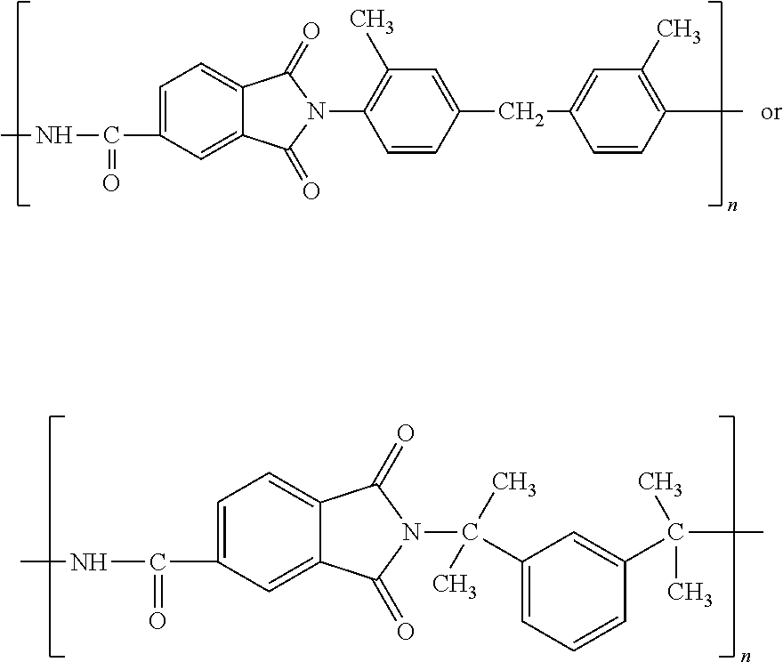
and wherein n represents a number of from about 40 to about 500; a photoconductor further including a silicone containing polyamideimide; a photoconductor wherein the silicone containing polyamideimide is represented by

wherein R is alkyl, aryl, or mixtures thereof; m and n represent the number of segments, and where the sum of m plus n is, for example, from about 10 to about 1,000, from about 75 to about 700, from about 125 to about 500, from about 150 to about 300; a photoconductor wherein m is from about 5 to about 500, n is from about 2 to about 500, Mw is from about 3,000 to about 50,000, Mn is from about 1,000 to about 20,000 with Mw and Mn being determined by known methods such as GPC; R is alkyl with from 1 to about 6 carbon atoms, and the silicone containing polyamideimide has a glass transition temperature of from about 255° C. to about 325° C.; a photoconductor comprising a substrate, a photogenerating layer, and a charge transport layer, and wherein the charge transport layer contains a polyamideimide; a photoconductor comprising a substrate, an undercoat layer thereover, a photogenerating layer, and at least one charge transport layer, and wherein the at least one charge transport layer in contact with the photogenerating layer contains a polyamideimide present in an amount of from about 0.1 to about 30 weight percent, from 1 to about 20 weight percent, from 2 to about 10 weight percent, more specifically about 1, 2, 3 or 4, and yet more specifically, about 2 weight percent; a photoconductor comprised in sequence of a photogenerating layer comprised of a photogenerating pigment, and a charge transport layer, and wherein the transport layer is comprised of a charge transport component and a polyamideimide with a suitable glass transition temperature of, for example, from about 200° C. to about 400° C., from about 220° C. to about 350° C., and from about 240° C. to about 300° C. determined by Differential Scanning calorimetry (DSC); a photoconductor comprising a supporting substrate, a ground plane layer, a hole blocking layer, a photogenerating layer comprised of at least one photogenerating pigment, and at least one charge transport layer comprised of at least one charge transport component, and where the charge transport layer has incorporated therein a polyamideimide available from Toyobo America, Inc., New York, N.Y.; a flexible photoconductive member comprised in sequence of a supporting substrate, a ground plane layer, a hole blocking or undercoat layer, a photogenerating layer thereover comprised of at least one photogenerating pigment, and a polyamideimide containing charge transport layer; a photoconductor which includes a hole blocking layer and an adhesive layer where the adhesive layer is situated between the hole blocking layer and the photogenerating layer, and the hole blocking layer is situated between the supporting substrate layer, and the adhesive layer; a photoconductor comprising a supporting substrate, a hole blocking layer, a photogenerating layer, and at least one charge transport layer comprised of at least one charge transport component, and wherein the first pass charge transport layer is in contact with the photogenerating layer, the second pass charge transport layer is in contact with the first charge transport layer, and the second pass charge transport layer includes therein a polyamideimide, a hole transport component, and a resin binder; a photoconductor comprising a supporting substrate, a photogenerating layer in contact with the supporting substrate, and at least one charge transport layer in contact with the photogenerating layer, and wherein at least one, such as 1, 2, or 3 charge transport layers, contains a polyamideimide as illustrated herein; a photoconductor comprised in sequence of a photogenerating layer comprised of a photogenerating pigment, such as a hydroxygallium phthalocyanine or a titanyl phthalocyanine, a first charge transport layer, and a second charge transport layer thereover, and wherein the second charge transport layer is comprised of a charge transport component and a polyamideimide as represented by or encompassed by

wherein n represents the number of repeating units, and Ar represents aryl with, for example, from 6 to about 42 carbons. More specifically, n can be a number of from about 20 to about 1,000, from about 40 to about 750, and from about 80 to about 500, and where the polyamideimide weight average molecular weight is, for example, from about 5,000 to about 200,000, or from about 10,000 to about 100,000, and the polyamideimide number average molecular weight is, for example, from about 2,000 to about 40,000, or from about 4,000 to about 20,000, and wherein the weight and number average molecular weights, Mw and Mn respectively, are determined by Gel Permeation Chromatography (GPC) analysis.
wherein R1 is an alkylene group containing, for example, from 1 to about 25 carbon atoms; R2 and R3 are independently selected from the group consisting of at least one of hydrogen or alkyl containing, for example, from 1 to about 12 carbon atoms, and more specifically, from 1 to about 4 carbon atoms; aryl with, for example, from about 6 to about 42 carbon atoms, such as a phenyl group; and a poly(alkylene like ethylene amino) group; and R4, R5 and R6 are independently selected from an alkyl group containing, for example, from 1 to about 10 carbon atoms, and more specifically, from 1 to about 4 carbon atoms.
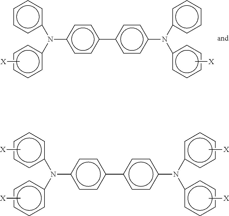
wherein X is a suitable hydrocarbon like alkyl, alkoxy, aryl, and derivatives thereof; a halogen, or mixtures thereof, and especially those substituents selected from the group consisting of Cl and CH3; and molecules of the following formulas

wherein X, Y and Z are independently alkyl, alkoxy, aryl, a halogen, or mixtures thereof, and wherein at least one of Y and Z are present.

wherein X is selected from the group consisting of alkyl, alkoxy, aryl, and halogen; an imaging member wherein alkyl and alkoxy contains from about 1 to about 12 carbon atoms; an imaging member wherein alkyl contains from about 1 to about 5 carbon atoms; an imaging member wherein alkyl is methyl: an imaging member wherein each of, or at least one of the charge transport layers comprises

wherein X and Y are independently alkyl, alkoxy, aryl, a halogen, or mixtures thereof; an imaging member wherein alkyl and alkoxy for the charge transport component aryl amine contain from about 1 to about 12 carbon atoms; an imaging member wherein alkyl contains from about 1 to about 5 carbon atoms, and wherein the resinous binder is selected from the group consisting of polycarbonates and polystyrene; an imaging member wherein the photogenerating pigment present in the photogenerating layer is comprised of chlorogallium phthalocyanine, or Type V hydroxygallium phthalocyanine prepared by hydrolyzing a gallium phthalocyanine precursor by dissolving the hydroxygallium phthalocyanine in a strong acid, and then reprecipitating the resulting dissolved precursor in a basic aqueous media; removing any ionic species formed by washing with water; concentrating the resulting aqueous slurry comprised of water and hydroxygallium phthalocyanine to a wet cake; removing water from the wet cake by drying; and subjecting the resulting dry pigment to mixing with the addition of a second solvent to cause the formation of the hydroxygallium phthalocyanine; an imaging member wherein the Type V hydroxygallium phthalocyanine has major peaks, as measured with an X-ray diffractometer, at Bragg angles (2 theta+/−0.2°) 7.4, 9.8, 12.4, 16.2, 17.6, 18.4, 21.9, 23.9, 25.0, 28.1 degrees, and the highest peak at 7.4 degrees: a method of imaging which comprises generating an electrostatic latent image on an imaging member developing the latent image, and transferring the developed electrostatic image to a suitable substrate; a method of imaging wherein the imaging member is exposed to light of a wavelength of from about 370 to about 950 nanometers; a photoconductive member wherein the photogenerating layer is situated between the substrate and the charge transport: a member wherein the charge transport layer is situated between the substrate and the photogenerating layer; a member wherein the photogenerating layer is of a thickness of from about 0.1 to about 50 microns; a member wherein the photogenerating pigment is dispersed in from about 1 weight percent to about 80 weight percent of a polymer binder; a member wherein the binder is present in an amount of from about 50 to about 90 percent by weight, and wherein the total of the layer components is about 100 percent; an imaging member wherein the photogenerating component is Type V hydroxygallium phthalocyanine, Type V titanyl phthalocyanine or chlorogallium phthalocyanine, and the charge transport layer contains a hole transport of N,N′-diphenyl-N,N-bis(3-methylphenyl)-1,1′-biphenyl-4,4′-diamine, N,N′-bis(4-butylphenyl)-N,N′-di-p-tolyl-[p-terphenyl]-4,4′-diamine. N,N′-bis(4-butylphenyl)-N,N′-di-m-tolyl-[p-terphenyl]-4,4′-diamine, N,N′-bis(4-butylphenyl)-N, N′-di-o-tolyl-[p-terphenyl]-4,4′-diamine, N,N′-bis(4-butylphenyl)-N, N′-bis-(4-isopropylphenyl)-[p-terphenyl]-4,4′-diamine, N,N′-bis(4-butylphenyl)-N, N′-bis-(2-ethyl-6-methylphenl)-[p-terphenyl]-4,4′-diamine. N,N′-bis(4-butylphenyl)-N,N′-bis-(2,5-dimethylphenyl)-[p-terphenyl]-4,4′-diamine, N,N′-diphenyl-N,N′-bis(3-chlorophenyl)-[p-terphenyl]-4,4′-diamine molecules, and wherein the hole transport resinous binder is selected from the group consisting of polycarbonates and polystyrene; an imaging member wherein the photogenerating layer contains a metal free phthalocyanine: a photoconductor wherein the photogenerating layer contains an alkoxygallium phthalocyanine; photoconductive imaging members comprised of a supporting substrate, a photogenerating layer, a hole transport layer, and in embodiments wherein a plurality of charge transport layers are selected, such as for example, from two to about ten, and more specifically two may be selected; and a photoconductive imaging member comprised of an optional supporting substrate, a photogenerating layer, and a first, second, and third charge transport layer.

| TABLE 1 | ||
| Wear Rate | ||
| (Nanometers/ | ||
| Kilocycle) | ||
| Comparative Example 1 (No Additive in CTL) | 60 |
| Comparative Example 2 (9.1% of PTFE in CTL) | 31 |
| Example I (2% of the Polyamideimide in CTL) | 34 |
Claims (34)


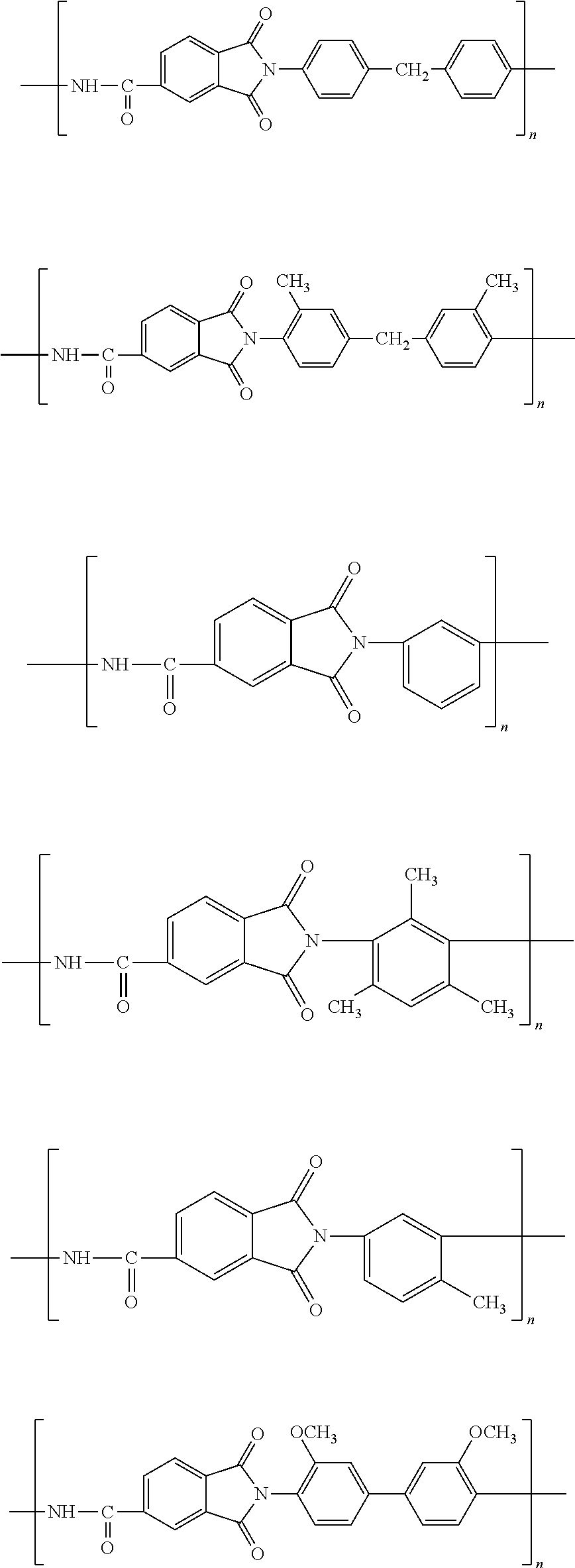


Priority Applications (1)
| Application Number | Priority Date | Filing Date | Title |
|---|---|---|---|
| US12/695,420 US8329367B2 (en) | 2010-01-28 | 2010-01-28 | Polyamideimide containing photoconductors |
Applications Claiming Priority (1)
| Application Number | Priority Date | Filing Date | Title |
|---|---|---|---|
| US12/695,420 US8329367B2 (en) | 2010-01-28 | 2010-01-28 | Polyamideimide containing photoconductors |
Publications (2)
| Publication Number | Publication Date |
|---|---|
| US20110183245A1 US20110183245A1 (en) | 2011-07-28 |
| US8329367B2 true US8329367B2 (en) | 2012-12-11 |
Family
ID=44309211
Family Applications (1)
| Application Number | Title | Priority Date | Filing Date |
|---|---|---|---|
| US12/695,420 Active 2031-05-27 US8329367B2 (en) | 2010-01-28 | 2010-01-28 | Polyamideimide containing photoconductors |
Country Status (1)
| Country | Link |
|---|---|
| US (1) | US8329367B2 (en) |
Families Citing this family (1)
| Publication number | Priority date | Publication date | Assignee | Title |
|---|---|---|---|---|
| JP6891900B2 (en) * | 2016-10-06 | 2021-06-18 | 株式会社豊田自動織機 | Negative electrode binder, intermediate composition, negative electrode, power storage device, polymer compound manufacturing method, and negative electrode electrode manufacturing method for power storage device |
Citations (5)
| Publication number | Priority date | Publication date | Assignee | Title |
|---|---|---|---|---|
| US4265990A (en) | 1977-05-04 | 1981-05-05 | Xerox Corporation | Imaging system with a diamine charge transport material in a polycarbonate resin |
| JPS63274960A (en) * | 1987-05-06 | 1988-11-11 | Matsushita Electric Ind Co Ltd | Electrophotographic sensitive body |
| US4921773A (en) * | 1988-12-30 | 1990-05-01 | Xerox Corporation | Process for preparing an electrophotographic imaging member |
| US20060257767A1 (en) * | 2005-05-11 | 2006-11-16 | Xerox Corporation | Imaging member |
| US20080057424A1 (en) * | 2006-08-31 | 2008-03-06 | Xerox Corporation | Overcoat for electrophotographic imaging member and methods of making and using same |
-
2010
- 2010-01-28 US US12/695,420 patent/US8329367B2/en active Active
Patent Citations (5)
| Publication number | Priority date | Publication date | Assignee | Title |
|---|---|---|---|---|
| US4265990A (en) | 1977-05-04 | 1981-05-05 | Xerox Corporation | Imaging system with a diamine charge transport material in a polycarbonate resin |
| JPS63274960A (en) * | 1987-05-06 | 1988-11-11 | Matsushita Electric Ind Co Ltd | Electrophotographic sensitive body |
| US4921773A (en) * | 1988-12-30 | 1990-05-01 | Xerox Corporation | Process for preparing an electrophotographic imaging member |
| US20060257767A1 (en) * | 2005-05-11 | 2006-11-16 | Xerox Corporation | Imaging member |
| US20080057424A1 (en) * | 2006-08-31 | 2008-03-06 | Xerox Corporation | Overcoat for electrophotographic imaging member and methods of making and using same |
Non-Patent Citations (7)
| Title |
|---|
| English language translation of JP 63-274960 (Nov. 1998). * |
| Jin Wu et al., U.S. Appl. No. 12/550,498 on Plasticizer Containing Photoconductors, filed Aug. 31, 2009. |
| Jin Wu, U.S. Appl. No. 12/644,112 on Sulfonamide Containing Photoconductors, filed Dec. 22, 2009. |
| Robert C.U. Yu et al., U.S. Appl. No. 12/434,572 on Flexible Imaging Members Without Anticurl Layer, filed May 1, 2009. |
| Robert C.U. Yu et al., U.S. Appl. No. 12/471,311 on Flexible Imaging Members Having a Plasticized Imaging Layer, filed May 22, 2009. |
| Robert C.U. Yu et al., U.S. Appl. No. 12/551,414 on Flexible Imaging Member Belts, filed Aug. 31, 2009. |
| Robert C.U. Yu et al., U.S. Appl. No. 12/551,440 on Flexible Imaging Member Belts, filed Aug. 31, 2009. |
Also Published As
| Publication number | Publication date |
|---|---|
| US20110183245A1 (en) | 2011-07-28 |
Similar Documents
| Publication | Publication Date | Title |
|---|---|---|
| US7811732B2 (en) | Titanocene containing photoconductors | |
| US7541122B2 (en) | Photoconductor having silanol-containing charge transport layer | |
| US7776499B2 (en) | Overcoat containing fluorinated poly(oxetane) photoconductors | |
| US8012657B2 (en) | Phenol polysulfide containing photogenerating layer photoconductors | |
| US8168357B2 (en) | Polyfluorinated core shell photoconductors | |
| US7560206B2 (en) | Photoconductors with silanol-containing photogenerating layer | |
| US8623578B2 (en) | Tetraaryl polycarbonate containing photoconductors | |
| US8067137B2 (en) | Polymer containing charge transport photoconductors | |
| US7871746B2 (en) | Thiophthalimides containing photoconductors | |
| US7960080B2 (en) | Oxadiazole containing photoconductors | |
| US9069268B2 (en) | Polyarylatecarbonate fluoropolymer containing photoconductors | |
| US7989126B2 (en) | Metal mercaptoimidazoles containing photoconductors | |
| US8426092B2 (en) | Poly(imide-carbonate) polytetrafluoroethylene containing photoconductors | |
| US8158315B2 (en) | SN containing hole blocking layer photoconductor | |
| US20110053065A1 (en) | Plasticizer containing photoconductors | |
| US8268520B2 (en) | Polyalkylene glycol benzoate polytetrafluoroethylene containing photoconductors | |
| US8304152B2 (en) | Spirodilactam polycarbonate containing photoconductors | |
| US7732111B2 (en) | Photoconductors containing halogenated binders and aminosilanes in hole blocking layer | |
| US8785091B1 (en) | Polyarylatecarbonate containing photoconductors | |
| US7993805B2 (en) | Polyalkylene glycol benzoate containing photoconductors | |
| US8318394B2 (en) | Sulfonamide containing photoconductors | |
| US8329367B2 (en) | Polyamideimide containing photoconductors | |
| US8168358B2 (en) | Polysulfone containing photoconductors | |
| US8535859B2 (en) | Photoconductors containing biaryl polycarbonate charge transport layers | |
| CA2981837C (en) | Polycarbonate containing photoconductors |
Legal Events
| Date | Code | Title | Description |
|---|---|---|---|
| AS | Assignment |
Owner name: XEROX CORPORATION, CONNECTICUT Free format text: ASSIGNMENT OF ASSIGNORS INTEREST;ASSIGNORS:WU, JIN , ,;TONG, YUHUA , ,;FERRARESE, LINDA L, ,;AND OTHERS;SIGNING DATES FROM 20100126 TO 20100127;REEL/FRAME:023866/0744 |
|
| FEPP | Fee payment procedure |
Free format text: PAYOR NUMBER ASSIGNED (ORIGINAL EVENT CODE: ASPN); ENTITY STATUS OF PATENT OWNER: LARGE ENTITY |
|
| STCF | Information on status: patent grant |
Free format text: PATENTED CASE |
|
| FPAY | Fee payment |
Year of fee payment: 4 |
|
| MAFP | Maintenance fee payment |
Free format text: PAYMENT OF MAINTENANCE FEE, 8TH YEAR, LARGE ENTITY (ORIGINAL EVENT CODE: M1552); ENTITY STATUS OF PATENT OWNER: LARGE ENTITY Year of fee payment: 8 |
|
| AS | Assignment |
Owner name: CITIBANK, N.A., AS AGENT, DELAWARE Free format text: SECURITY INTEREST;ASSIGNOR:XEROX CORPORATION;REEL/FRAME:062740/0214 Effective date: 20221107 |
|
| AS | Assignment |
Owner name: XEROX CORPORATION, CONNECTICUT Free format text: RELEASE OF SECURITY INTEREST IN PATENTS AT R/F 062740/0214;ASSIGNOR:CITIBANK, N.A., AS AGENT;REEL/FRAME:063694/0122 Effective date: 20230517 |
|
| AS | Assignment |
Owner name: CITIBANK, N.A., AS COLLATERAL AGENT, NEW YORK Free format text: SECURITY INTEREST;ASSIGNOR:XEROX CORPORATION;REEL/FRAME:064760/0389 Effective date: 20230621 |
|
| AS | Assignment |
Owner name: JEFFERIES FINANCE LLC, AS COLLATERAL AGENT, NEW YORK Free format text: SECURITY INTEREST;ASSIGNOR:XEROX CORPORATION;REEL/FRAME:065628/0019 Effective date: 20231117 |
|
| AS | Assignment |
Owner name: CITIBANK, N.A., AS COLLATERAL AGENT, NEW YORK Free format text: SECURITY INTEREST;ASSIGNOR:XEROX CORPORATION;REEL/FRAME:066741/0001 Effective date: 20240206 |