US8334945B2 - Liquid crystal display device - Google Patents
Liquid crystal display device Download PDFInfo
- Publication number
- US8334945B2 US8334945B2 US12/007,091 US709108A US8334945B2 US 8334945 B2 US8334945 B2 US 8334945B2 US 709108 A US709108 A US 709108A US 8334945 B2 US8334945 B2 US 8334945B2
- Authority
- US
- United States
- Prior art keywords
- light
- liquid crystal
- guide panel
- light guide
- display device
- Prior art date
- Legal status (The legal status is an assumption and is not a legal conclusion. Google has not performed a legal analysis and makes no representation as to the accuracy of the status listed.)
- Active, expires
Links
- 239000004973 liquid crystal related substance Substances 0.000 title claims abstract description 68
- 239000000853 adhesive Substances 0.000 claims abstract description 18
- 230000001070 adhesive effect Effects 0.000 claims abstract description 18
- 230000001678 irradiating effect Effects 0.000 claims abstract description 8
- 239000000758 substrate Substances 0.000 claims description 46
- 239000000463 material Substances 0.000 claims description 9
- 239000003973 paint Substances 0.000 claims description 5
- 230000007423 decrease Effects 0.000 claims 3
- 230000003287 optical effect Effects 0.000 abstract description 41
- 238000000034 method Methods 0.000 description 10
- 239000011347 resin Substances 0.000 description 9
- 229920005989 resin Polymers 0.000 description 9
- 238000009792 diffusion process Methods 0.000 description 8
- 239000002245 particle Substances 0.000 description 6
- 238000010586 diagram Methods 0.000 description 4
- 238000004806 packaging method and process Methods 0.000 description 4
- 239000010410 layer Substances 0.000 description 3
- 230000001902 propagating effect Effects 0.000 description 3
- 239000004065 semiconductor Substances 0.000 description 3
- 239000012790 adhesive layer Substances 0.000 description 2
- 238000005352 clarification Methods 0.000 description 2
- 238000004519 manufacturing process Methods 0.000 description 2
- 239000011159 matrix material Substances 0.000 description 2
- 230000010287 polarization Effects 0.000 description 2
- 239000004925 Acrylic resin Substances 0.000 description 1
- 229920000178 Acrylic resin Polymers 0.000 description 1
- 230000000903 blocking effect Effects 0.000 description 1
- 239000003086 colorant Substances 0.000 description 1
- 230000000694 effects Effects 0.000 description 1
- 230000000717 retained effect Effects 0.000 description 1
- 229910052709 silver Inorganic materials 0.000 description 1
- 239000004332 silver Substances 0.000 description 1
- 229910000679 solder Inorganic materials 0.000 description 1
Images


Classifications
-
- G—PHYSICS
- G02—OPTICS
- G02B—OPTICAL ELEMENTS, SYSTEMS OR APPARATUS
- G02B6/00—Light guides; Structural details of arrangements comprising light guides and other optical elements, e.g. couplings
- G02B6/0001—Light guides; Structural details of arrangements comprising light guides and other optical elements, e.g. couplings specially adapted for lighting devices or systems
- G02B6/0011—Light guides; Structural details of arrangements comprising light guides and other optical elements, e.g. couplings specially adapted for lighting devices or systems the light guides being planar or of plate-like form
- G02B6/0033—Means for improving the coupling-out of light from the light guide
- G02B6/005—Means for improving the coupling-out of light from the light guide provided by one optical element, or plurality thereof, placed on the light output side of the light guide
- G02B6/0055—Reflecting element, sheet or layer
-
- G—PHYSICS
- G02—OPTICS
- G02B—OPTICAL ELEMENTS, SYSTEMS OR APPARATUS
- G02B6/00—Light guides; Structural details of arrangements comprising light guides and other optical elements, e.g. couplings
- G02B6/0001—Light guides; Structural details of arrangements comprising light guides and other optical elements, e.g. couplings specially adapted for lighting devices or systems
- G02B6/0011—Light guides; Structural details of arrangements comprising light guides and other optical elements, e.g. couplings specially adapted for lighting devices or systems the light guides being planar or of plate-like form
- G02B6/0066—Light guides; Structural details of arrangements comprising light guides and other optical elements, e.g. couplings specially adapted for lighting devices or systems the light guides being planar or of plate-like form characterised by the light source being coupled to the light guide
- G02B6/0073—Light emitting diode [LED]
-
- G—PHYSICS
- G02—OPTICS
- G02B—OPTICAL ELEMENTS, SYSTEMS OR APPARATUS
- G02B6/00—Light guides; Structural details of arrangements comprising light guides and other optical elements, e.g. couplings
- G02B6/0001—Light guides; Structural details of arrangements comprising light guides and other optical elements, e.g. couplings specially adapted for lighting devices or systems
- G02B6/0011—Light guides; Structural details of arrangements comprising light guides and other optical elements, e.g. couplings specially adapted for lighting devices or systems the light guides being planar or of plate-like form
- G02B6/0033—Means for improving the coupling-out of light from the light guide
- G02B6/0035—Means for improving the coupling-out of light from the light guide provided on the surface of the light guide or in the bulk of it
- G02B6/0038—Linear indentations or grooves, e.g. arc-shaped grooves or meandering grooves, extending over the full length or width of the light guide
-
- G—PHYSICS
- G02—OPTICS
- G02B—OPTICAL ELEMENTS, SYSTEMS OR APPARATUS
- G02B6/00—Light guides; Structural details of arrangements comprising light guides and other optical elements, e.g. couplings
- G02B6/0001—Light guides; Structural details of arrangements comprising light guides and other optical elements, e.g. couplings specially adapted for lighting devices or systems
- G02B6/0011—Light guides; Structural details of arrangements comprising light guides and other optical elements, e.g. couplings specially adapted for lighting devices or systems the light guides being planar or of plate-like form
- G02B6/0081—Mechanical or electrical aspects of the light guide and light source in the lighting device peculiar to the adaptation to planar light guides, e.g. concerning packaging
- G02B6/0083—Details of electrical connections of light sources to drivers, circuit boards, or the like
Definitions
- the present invention relates to a light source for a non-self-luminous display device, and more particularly to a liquid crystal display device having a light guide panel and a back light using an LED as a light source.
- liquid crystal display devices are widely used as display devices. Since the liquid crystal display devices are especially thin, light, and thrifty in power consumption, they are often used as display sections of portable devices.
- a lighting unit is generally used as a lighting unit for the liquid crystal display device.
- Cold cathode discharge tubes have been used as light-emitting elements (also referred to as light sources) heretofore; recently, LEDs (light emitting diodes) are also used as light-emitting elements.
- a plate-like light guide panel is provided in a back light.
- the light guide panel is made of translucent resin or the like, and light entering the light guide panel from a light-emitting element propagates through the light guide panel.
- Provided in the light guide panel are light-reflective and dispersal members such as grooves, projections, or printed materials. The light propagating through the light guide panel by these light-reflective and dispersal members goes out of the light guide panel toward the liquid crystal display device side.
- an FPC Flexible Printed Circuit
- a portion of the FPC be overlaid on the light guide panel.
- the frame width of the back light (the width of an area where light is not emitted)
- a display panel Provided in a liquid crystal display device are a display panel, a back light for irradiating the display panel with light, a light emitting element provided in the back light, a light guide panel into which light from the light emitting element is introduced, and a circuit board on which the light emitting element is mounted. Furthermore, an optical sheet is placed on the light guide panel, a colored area formed with a reflective member is provided in a portion of the optical sheet, and the colored area is provided between the light guide panel and the circuit board.
- the circuit board on which the light emitting element is mounted and the optical sheet are fixed to each other with an adhesive, and the light emitting element is positioned with respect to the optical sheet.
- the colored area formed with a reflective member is provided in a portion of the optical sheet, and the colored area is provided between the light guide panel and the circuit board on which the light emitting element is provided, the light absorbed in the circuit board can be guided to the light guide panel side.
- FIG. 1 is a schematic block diagram illustrating a configuration of a liquid crystal display device according to an embodiment of the present invention
- FIGS. 2A and 2B are schematic block diagrams illustrating a light-emitting diode of the liquid crystal display device according to the embodiment of the present invention.
- FIGS. 3A and 3B are schematic block diagrams illustrating a light guide panel of the liquid crystal display device according to the embodiment of the present invention.
- FIGS. 4A and B are schematic cross-sectional views illustrating propagation of a light beam through the light guide panel of the liquid crystal display device according to the embodiment of the present invention.
- FIG. 5 is a schematic illustrating positions of the light guide panel and light-emitting diode of the liquid crystal display device according to the embodiment of the present invention.
- FIG. 6 is a schematic showing a method of packaging the light guide panel in the liquid crystal display device according to the embodiment of the present invention.
- FIG. 7 is a schematic showing a method of packaging the light guide panel in the liquid crystal display device according to the embodiment of the present invention.
- FIG. 8 is a schematic perspective view illustrating a back light of the liquid crystal display device according to the embodiment of the present invention.
- FIG. 9 is a schematic cross-sectional view illustrating the back light in the liquid crystal display device according to the embodiment of the present invention.
- FIG. 10 is a schematic cross-sectional view illustrating propagation of light through the light guide panel of the liquid crystal display device according to the embodiment of the present invention.
- FIG. 11 is a schematic perspective view illustrating the back light of the liquid crystal display device according to the embodiment of the present invention.
- FIG. 12 is a schematic plan view illustrating an optical sheet of the liquid crystal display device according to the embodiment of the present invention.
- FIG. 13 is a schematic perspective view illustrating the optical sheet of the liquid crystal display device according to the embodiment of the present invention.
- FIG. 14 is a schematic cross-sectional view illustrating the optical sheet of the liquid crystal display device according to the embodiment of the present invention.
- a liquid crystal display device having a liquid crystal panel and a planar lighting unit for irradiating the liquid crystal panel with light
- a light guide panel having a light outgoing face and a bottom face opposite to the light outgoing face is provided in the planar lighting unit.
- a side face intersecting with the light outgoing face or the bottom face is provided in the light guide panel.
- an LED is provided along a first side face of the light guide panel. A light beam from the LED is introduced from the first side face so that the first side face is defined as a light incoming face of the light guide panel.
- an LED is mounted on a circuit board.
- An optical sheet is provided on the light outgoing face of the light guide panel, a colored area is provided in a portion of the optical sheet, and the colored area is provided between the light guide panel and the optical sheet.
- FIG. 1 is a plan view illustrating a liquid crystal display device 100 according to the present invention.
- the liquid crystal display device 100 comprises a liquid crystal panel 1 , a back light 110 , and a control circuit 80 . Signals required for display on the liquid crystal display device 100 and a power voltage are supplied from the control circuit 80 .
- the control circuit 80 is mounted on a flexible substrate 70 , and signals are delivered to the liquid crystal panel 1 via wiring 71 and a terminal 75 .
- the back light 110 comprises a light guide panel 120 , an LED 150 , and a housing 180 .
- the back light 110 is provided to irradiate the liquid crystal panel 1 .
- displays are provided by controlling an amount of transmitted light or reflected light which is radiated from the back light 110 .
- the back light 110 is provided in an overlaid state on the back side or the front side of the liquid crystal panel 1 when viewed from a viewer, but in FIG. 1 , the back light 110 is juxtaposed with the liquid crystal panel 1 for a clarification purpose.
- the light guide panel 12 has a substantially rectangular form, and the LED 150 is provided on a side face of the light guide panel 120 .
- Reference numeral 160 denotes a flexible substrate for electrical connection among a plurality of LEDs 150 .
- the flexible substrate 160 and the control circuit 80 are electrically connected to each other by wiring 161 .
- a face of the light guide panel on which the LED 150 is mounted is referred to as a “light incoming plane”, and light from the light incoming plane 125 goes into the light guide panel 120 .
- a convex portion 220 (also referred to “projecting portion”) is provided between two adjoining LEDs 150 . This convex portion 220 is described in detail hereinafter.
- the liquid crystal panel 1 has two substrates, namely a TFT substrate 2 and a color filter substrate 3 , and a liquid crystal composition is held between the overlaid two substrates.
- a pixel electrode 12 is provided in a pixel section 8 of the TFT substrate 8 .
- the liquid crystal panel 1 has a number of pixel sections 8 provided in a matrix state, but in FIG. 1 , only one pixel section 8 is shown to evade complexity.
- the pixel sections 8 provided in the matrix state forms a display area 9 .
- Each of the pixel sections 8 plays a role of a pixel of a displayed image to display an image on the display area 9 .
- gate signal lines 21 also referred to as scan line
- drain signal lines 22 also referred to as video signal line
- the pixel section 8 is formed in an area surrounded by the gate signal line 21 and the rain signal line 22 .
- a switching element 10 is provided in the pixel section 8 . Control signals are supplied from the gate signal line 21 to turn ON/OFF the switching element 10 . When the switching element 10 is turned ON, a video signal transmitted via the drain signal 22 is supplied to the pixel electrode 12 .
- the drain signal line 22 is connected to a drive circuit 5 , and a video signal is output from the drive circuit 5 .
- the gate signal line 21 is connected to a drive circuit 6 , and a control signal is output from the drive circuit 6 .
- the gate signal line 21 , the drain signal line 22 , and the drive circuits 5 and 6 are formed on the same TFT substrates 2 .
- a configuration is also allowable in which the drive circuits 5 and 6 and the control circuit 80 are formed on the same semiconductor chip.
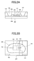
- FIG. 2 is a schematic block diagram illustrating the LED 150 which is a light-emitting element.
- FIG. 2A is a schematic cross-section illustrating the same, and
- FIG. 2B is a front view illustrating the LED 150 viewed from the light outgoing plane side.
- the LED 150 has a structure in which an LED 151 , a light-emitting section, is mounted on a chip substrate 154 .
- the LED chip 151 has a p-n junction, and when a voltage is applied to the p-n junction, light having a particular wavelength is output.
- a p electrode (anode) 158 is provided on a p-type semiconductor layer, and an n electrode (cathode) 159 is provided on an n-type semiconductor layer, which layers constitute the p-n junction.
- the p electrode 158 and the n electrode 159 are connected to each other via a wire 152 .
- the wire 152 electrically connects a chip terminal 153 provided to connect the LED 150 to the outside to the p electrode 158 as well as to the n electrode 159 .
- a fluorescence emitting section 156 may be provided on the light outgoing plane side of the LED chip 151 .
- the fluorescence emitting section 156 has a function of converting a wavelength of light emitted from the LED chip 151 .
- Reference numeral 155 denotes a reflection section which reflects light forward.
- FIG. 3A is a schematic plan view of the light guide panel 120 while FIG. 3B is a schematic cross-sectional view of the same.
- the light guide panel 120 has a substantially rectangular form as shown in FIG. 3A and has an upper face 121 and a lower face 122 as shown in FIG. 3B .
- the light guide panel 120 is made of an optically transmissive material such as acrylic resin and has a plate-like form, and its thickness is in the range from 1.0 mm to 0.2 mm.
- FIG. 3A is a plan view illustrating the lower face of the light guide panel 120 for clarification purposes.
- a cross section of the light guide panel 120 is substantially rectangular, and an inclined plane 129 is formed from the light incoming plane 125 toward the light outgoing plane 121 .
- This inclined plane 129 is effective when the thickness of the LED 150 is larger than the thickness of the light outgoing plane of the light guide panel, and the inclined plane 129 guides the light incoming from the light incoming plane 125 having a larger thickness than that of the light outgoing plane 121 toward the light outgoing plane 121 .
- FIG. 3 shows positional relations among the light guide panel 120 , the LED 150 , and the flexible substrate 160 .
- the light incoming plane 125 is provided on at least one side of the light guide panel 120 , and a plurality of LEDs 150 are provided at positions adjacent to the light incoming plane 125 .
- the LEDs 150 are arranged in the lower side of the flexible substrate 160 along the light incoming plane 125 .
- An adhesive sheet 190 is provided on the side of the light guide panel 120 of the flexible substrate 160 , and the LED 150 is positioned with respect to the light incoming plane 125 by adhering and fixing the flexible substrate 160 to a convex portion 220 of the light guide panel 120 .
- the inclined plane 129 is formed at a place adjacent to the light incoming plane 125 . Furthermore, the flexible substrate 160 is flexible. However, since the overlaid area of the inclined plane 129 with the flexible substrate is small, it is difficult to fold the flexible substrate 160 and fix the folded flexible substrate 160 with the adhesive sheet 190 to the inclined plane 129 . In addition, a position of the LED 150 may move after packaging due to a stress generated by folding. To prevent the trouble as described above, the convex portions 220 are formed in the light guide panel 120 along the side faces of the LEDs 150 , and the adhesive sheets 190 are provided between the convex portions 220 and the flexible substrate 160 .
- the light beam 131 radiated from the LED 150 goes into the light guide panel 120 from the light incoming plane 125 .
- the upper face 121 and the lower face 122 of the light guide panel 120 are perpendicular to the light incoming plane 125 , respectively, and a V-shaped groove 126 is provided as a reflection section on the lower face 122 .
- the light beams coming into the inside of the light guide panel 120 move forward in the light guide panel 120 being totally reflected on the upper face 121 and the lower face 122 of the light guide panel 120 repetitively.
- a portion of the light beam propagating in the light guide panel 120 is reflected toward the upper face 121 at the grooves 126 provided on the lower face 122 and goes out through the upper face 121 .
- V-shaped groove is described as an example of a reflection section, there is no specific restriction over the form of the groove 126 so long as the light beams propagating forward in the light guide panel are reflected toward the upper face 121 ; white dots may be used instead, for instance, by printing for the same purpose.
- FIG. 4A shows a case in which the groove 126 is concave
- FIG. 4B shows a case where the groove 126 is convex
- the groove 126 has a reflection plane (also referred to as inclined plane) 127
- the reflection plane 127 is inclined by 1 to 35 degrees with respect to the lower face 122 .
- the light beams reflected at the reflection plane 127 are reflected toward the upper face 121 of the light guide panel 120 , and an angle of reflection toward the upper face 121 is adjusted so that the reflected light beams can go out through the upper face 121 .
- the light beam may be reflected on the reflection plane 127 so that the it extends outward at a large angle with respect to the direction vertical to the upper face 121 of the light guide panel 120 (at a blunt angle with respect to the upper face 121 ).
- prism sheets 113 and 112 are provided on the light guide panel 120 so that the light beam moving outward is reflected toward a liquid crystal panel (not shown).
- Reference numeral 114 denotes a diffusion sheet
- reference numeral 115 denotes a reflection sheet.
- FIG. 5 a process for combining a flexible substrate 160 with the LED 150 mounted thereon with the light guide panel 120 is described with reference to FIG. 5 .
- the optical sheet placed on the light guide panel 120 is eliminated to clarify the positional relation between the flexible substrate 160 and the light guide panel 120 .
- the LED 150 is mounted on the flexible substrate 160 by being connected to a connection pad 165 formed on the flexible substrate 160 with such a material as solder.
- a connection pad 165 formed on the flexible substrate 160 with such a material as solder.
- wiring for supplying power to each LED 150 is provided on the flexible substrate 160 , the wiring is not shown in FIG. 5 for simplicity.
- the adhesive sheet 190 is provided on the flexible substrate 160 with the LED 150 mounted thereon, and the flexible substrate 160 is attached with the adhesive sheet 190 to a convex portion 220 of the light guide panel 120 . If the position of the LED 150 easily changes with respect to the light incoming plane 125 of the light guide panel 120 due to vibration or the like, brightness of the light which comes into the light guide panel 120 fluctuates, which spoils the stability of display performance. To prevent the trouble as described above, the flexible substrate 160 is fixed to the convex portion 220 of the light guide panel 120 with the adhesive sheet 190 or the like.
- the adhesive sheet 190 has a multilayer structure in which an adhesive member is provided on a resin substrate; also, it is possible to provide a reflection area on the substrate using paint or a material such as silver.
- the adhesive sheet 190 By forming a structure in which the light guide panel 120 and the flexible substrate 160 are integrated with each other by using the adhesive sheet 190 , it becomes possible to check whether the LED 150 is placed at a right position with respect to the light incoming plane 125 of the light guide panel 120 . In other words, if the flexible substrate 160 and the light guide panel 120 are packaged discretely in the back light during the production process and an attempt is made afterward to check a position of the LED 150 with respect to the light incoming plane 125 , that attempt would fail because the LED 150 and the light incoming plane 125 are hidden by other components.
- the mold 180 has a function as an accommodating section for the back light 110 . Housed and retained in the mold 180 are the light guide panel 120 and the flexible substrate 160 .
- the mold 180 also has a function for preventing leakage of light and covers the light guide panel 120 .
- the mold 180 has an opening on the side facing the liquid crystal panel so that a light beam from the back light 110 is radiated out of the opening to irradiate the liquid crystal panel.
- a reflection sheet 115 is placed on the mold 180 , and the light guide panel 120 and the flexible substrate 160 are placed over the reflection sheet 115 . Also the configuration is allowable in which an opening is provided on a bottom face of the mold 180 and the reflection sheet 115 is fixed with an adhesive to the external side of the opening as shown in FIG. 6 .
- the reflection sheet 115 When the reflection sheet 115 is provided on the external side of the opening of the mold 180 , it becomes possible to form a space between the LED 150 and the reflection sheet 115 . Further, it becomes possible to reduce the possibility of contact between the LED 150 and the reflection sheet 115 due to thermal expansion of the LED 150 .
- FIG. 7 shows a step of providing optical sheets such as the diffusion sheet 114 , the lower prism sheet 113 , the upper prism sheet 112 , or the like on the light guide panel 120 .
- the optical sheets are provided to efficiently irradiate the liquid crystal panel with the light beam radiated from the light guide panel 120 , and the optical sheets are placed in order on the light outgoing plane of the light guide panel 120 .
- each of the optical sheets are arranged according to the light which comes out of the light outgoing plane of the light guide panel 120 . Therefore, each of the optical sheets has the substantially same form and the substantially same size as those of the light outgoing plane of the light guide panel 120 . In other words, because areas of each optical sheet are required to be minimized to lower product prices, each of the optical sheets has only to be of the substantially same size as that of the light outgoing plane of the light guide panel 120 to achieve the optical object as described above.
- one of the optical sheets extends up to a position close to the LED 150 to form a colored area 211 with white ink on the light guide panel 120 side.
- the colored area 211 reflects a light beam coming out of the light guide panel 120 and returns the light beam toward the light guide panel 120 side.
- FIG. 8 shows a state in which optical sheets such as the diffusion sheet 114 , the lower prism sheet 113 , and the upper prism sheet 112 are provided on the light guide panel 120 and the flexible substrate 160 is provided on the uppermost optical sheet.
- the colored area 211 formed on the optical sheet (the upper prism sheet 112 ) is positioned between the light guide panel 120 and the flexible substrate 160 .
- the light beam radiated from the light guide panel 120 is reflected by the colored area 211 toward the light guide panel 120 without being absorbed by the flexible substrate 160 .
- FIG. 9 is a cross-sectional view of a structure in which the light guide panel 120 and other related components are packaged in the mold 180 and the liquid crystal panel 1 is mounted thereon.
- the liquid crystal panel 1 has a structure in which the color filter substrate 3 is placed on the TFT substrate 2 , and an upper polarization plate 231 and a lower polarization plate 232 are provided in the outer sides of the TFT substrate 2 and the color filter substrate 3 .
- the colored area 211 is provided on the optical sheet (upper prism sheet 112 ).
- the colored area 211 faces the inclined plane 129 of the light guide panel 120 and reflects the light beams radiated from the inclined plane 129 toward the light guide panel 120 .
- the critical angle of the light beam with respect to normal line directions of the upper face 121 and the lower face 122 of the light guide panel 120 is 38.97 degrees.
- the angle of a light beam 130 coming into the light guide panel 120 from the light incoming plane 125 with respect to normal line directions of the upper face 121 and the lower face 122 of the light guide panel 120 is more than 51.03 degrees, which is larger than the critical angle. Therefore, total reflection of the light beam is repeated.
- the colored area 211 is effective in again reflecting the light beam going out of the inclined plane 129 toward the light guide panel 120 . That is, when the angle 134 between the upper face 121 and the inclined plane 129 is more than ((90 degrees ⁇ critical angle) ⁇ critical angle) degrees, the colored area 211 is effective.
- the inclined plane 129 is provided to reduce the thickness of the light guide panel 120 in a section between the light incoming plane 125 and the upper face 121 when the thickness of the light guide panel 120 is smaller than that of the LED 150 , which enables use of the light guide panel 120 with a smaller thickness.
- FIG. 11 illustrates a state in which the optical sheet (upper prism sheet 112 ) extends up to the convex portion 220 of the light guide panel 120 and the upper prism sheet 112 is attached to the convex portion 220 with the adhesive member 190 .
- the flexible substrate 160 and the upper prism sheet 112 are attached to each other by providing an adhesive layer 212 on the side opposite to the colored member 211 on the optical sheet. That is, with the configuration in which a light reflection section is provided with such a material as white paint on the light guide panel 120 side of the optical sheet and a multi-layered structure with the adhesive layer 212 is provided on the flexible substrate 160 side of the optical sheet, positional alignment with the flexible substrate 160 can easily be performed. It is to be noted that the adhesive member 190 for adhesion between the light guide panel 120 and the upper prism sheet 112 is provided on the convex portion 220 .
- the colored area 211 is formed by printing or applying a suited material on a sheet-like base film 116 (a base material for the optical sheet). Then, the base film on which the colored area 211 is formed is stamped out in the form of the optical sheet 117 .
- a number of optical sheets 117 can be made from one sheet of the base film 116 .
- the colored areas 211 are formed on a rolled base film 118 in advance, or they are formed during the same process as the stamping-out process, and the optical sheets 117 are stamped out with the base film 118 with the colored areas 211 formed thereon rolled up.
- the use of the rolled base film 118 makes storage of the base film 118 easy; further, it improves work efficiency because the optical sheets 117 can be stamped out successively during the manufacturing process.
- FIG. 14 illustrates the colored area 211 provided on the diffusion sheet 114 formed by applying resin particles 118 on the resin-made base film 116 .
- the resin particles 118 are applied on the diffusion sheet 114 shown in FIG. 14 .
- the moving directions of light beams are diffused by the light beams being refracted with the resin particles 118 .
- the resin particles 118 are made of resin having the same refraction index as that of the base film 116 .
- Resin particles 119 for preventing adhesion are provided on the surface opposite to that on which the resin particles 118 for diffusion are provided, and the colored area 211 is provided on the same surface.
- the colored area 211 is formed on the light-guide-panel-side surface of optical sheets such as the prism sheet 112 or the diffusion sheet 114 .
- the same effect can be obtained even when the colored area 211 is formed on the surface of the optical sheet opposite to that facing the light guide panel 120 , for the thickness of the prism sheet 113 or the diffusion sheet 114 is very small, namely about 50 ⁇ m.
Abstract
Description
Claims (12)
Applications Claiming Priority (2)
| Application Number | Priority Date | Filing Date | Title |
|---|---|---|---|
| JP2007-003977 | 2007-01-12 | ||
| JP2007003977A JP2008170739A (en) | 2007-01-12 | 2007-01-12 | Liquid crystal display device |
Publications (2)
| Publication Number | Publication Date |
|---|---|
| US20080170174A1 US20080170174A1 (en) | 2008-07-17 |
| US8334945B2 true US8334945B2 (en) | 2012-12-18 |
Family
ID=39617467
Family Applications (1)
| Application Number | Title | Priority Date | Filing Date |
|---|---|---|---|
| US12/007,091 Active 2031-03-09 US8334945B2 (en) | 2007-01-12 | 2008-01-07 | Liquid crystal display device |
Country Status (2)
| Country | Link |
|---|---|
| US (1) | US8334945B2 (en) |
| JP (1) | JP2008170739A (en) |
Families Citing this family (18)
| Publication number | Priority date | Publication date | Assignee | Title |
|---|---|---|---|---|
| KR101450810B1 (en) * | 2008-06-02 | 2014-10-14 | 삼성디스플레이 주식회사 | Backlight assembly and display device having the same |
| USRE45912E1 (en) | 2008-06-30 | 2016-03-01 | Mitsuba Corporation | Electric motor |
| JP5221657B2 (en) * | 2008-07-08 | 2013-06-26 | シャープ株式会社 | Liquid crystal display |
| JP5198324B2 (en) * | 2009-02-25 | 2013-05-15 | ミネベア株式会社 | Surface lighting device |
| TWM381090U (en) * | 2009-11-12 | 2010-05-21 | Chunghwa Picture Tubes Ltd | Display module |
| JP5586237B2 (en) | 2010-01-07 | 2014-09-10 | 株式会社ジャパンディスプレイ | Liquid crystal display |
| JP2011203639A (en) | 2010-03-26 | 2011-10-13 | Hitachi Displays Ltd | Liquid crystal display device |
| JP5857496B2 (en) * | 2011-07-25 | 2016-02-10 | セイコーエプソン株式会社 | LIGHTING DEVICE, DISPLAY DEVICE, AND ELECTRONIC DEVICE |
| JP5725349B2 (en) | 2011-07-25 | 2015-05-27 | ミネベア株式会社 | Surface lighting device |
| WO2013161241A1 (en) * | 2012-04-26 | 2013-10-31 | シャープ株式会社 | Backlight unit and liquid crystal display apparatus |
| KR20140018742A (en) | 2012-08-03 | 2014-02-13 | 삼성디스플레이 주식회사 | Backlight unit and display apparatus having the same |
| JP2014048385A (en) * | 2012-08-30 | 2014-03-17 | Japan Display Inc | Liquid crystal display device |
| CN103018959B (en) * | 2012-12-26 | 2015-12-02 | 深圳市华星光电技术有限公司 | A kind of liquid crystal module |
| JP5440989B1 (en) | 2013-02-25 | 2014-03-12 | ミネベア株式会社 | Surface lighting device |
| JP5784769B2 (en) | 2014-02-12 | 2015-09-24 | ミネベア株式会社 | Surface lighting device |
| JP6220765B2 (en) * | 2014-11-25 | 2017-10-25 | ミネベアミツミ株式会社 | Surface lighting device |
| KR102530803B1 (en) * | 2016-08-31 | 2023-05-10 | 엘지디스플레이 주식회사 | Liquid crystal display device |
| CN108319075B (en) * | 2018-01-31 | 2020-09-04 | Oppo广东移动通信有限公司 | Electronic device, display assembly and backlight module thereof |
Citations (7)
| Publication number | Priority date | Publication date | Assignee | Title |
|---|---|---|---|---|
| US5521797A (en) * | 1993-02-01 | 1996-05-28 | Tosoh Corporation | Backlighting device |
| US6411353B1 (en) * | 1998-04-22 | 2002-06-25 | Hitachi, Ltd. | Liquid crystal display device with its upper and lower cases clamped by crimping portions thereof |
| US6825894B2 (en) * | 2001-05-30 | 2004-11-30 | Hitachi, Ltd. | Liquid crystal display device |
| US6942374B2 (en) * | 2002-12-05 | 2005-09-13 | Samsung Electronics Co., Ltd. | Backlight assembly and liquid crystal display apparatus having the same |
| JP2005251687A (en) | 2004-03-08 | 2005-09-15 | Minebea Co Ltd | Surface lighting device |
| US20060056200A1 (en) * | 2003-01-29 | 2006-03-16 | Tomoyoshi Yamashita | Area light source |
| US20070008739A1 (en) * | 2005-07-06 | 2007-01-11 | Samsung Electro-Mechanics Co., Ltd. | Light source-guide structure of backlight apparatus with LED light source inserted into light guide plate and backlight apparatus having the same |
-
2007
- 2007-01-12 JP JP2007003977A patent/JP2008170739A/en active Pending
-
2008
- 2008-01-07 US US12/007,091 patent/US8334945B2/en active Active
Patent Citations (7)
| Publication number | Priority date | Publication date | Assignee | Title |
|---|---|---|---|---|
| US5521797A (en) * | 1993-02-01 | 1996-05-28 | Tosoh Corporation | Backlighting device |
| US6411353B1 (en) * | 1998-04-22 | 2002-06-25 | Hitachi, Ltd. | Liquid crystal display device with its upper and lower cases clamped by crimping portions thereof |
| US6825894B2 (en) * | 2001-05-30 | 2004-11-30 | Hitachi, Ltd. | Liquid crystal display device |
| US6942374B2 (en) * | 2002-12-05 | 2005-09-13 | Samsung Electronics Co., Ltd. | Backlight assembly and liquid crystal display apparatus having the same |
| US20060056200A1 (en) * | 2003-01-29 | 2006-03-16 | Tomoyoshi Yamashita | Area light source |
| JP2005251687A (en) | 2004-03-08 | 2005-09-15 | Minebea Co Ltd | Surface lighting device |
| US20070008739A1 (en) * | 2005-07-06 | 2007-01-11 | Samsung Electro-Mechanics Co., Ltd. | Light source-guide structure of backlight apparatus with LED light source inserted into light guide plate and backlight apparatus having the same |
Also Published As
| Publication number | Publication date |
|---|---|
| JP2008170739A (en) | 2008-07-24 |
| US20080170174A1 (en) | 2008-07-17 |
Similar Documents
| Publication | Publication Date | Title |
|---|---|---|
| US8334945B2 (en) | Liquid crystal display device | |
| US7808576B2 (en) | Liquid crystal display device | |
| JP5142495B2 (en) | Liquid crystal display | |
| TWI381224B (en) | Liquid crystal display device | |
| JP5091602B2 (en) | Surface light source device and liquid crystal display device using the same | |
| KR101299130B1 (en) | Liquid crystal display device | |
| JP2008015288A (en) | Liquid crystal display | |
| JP4939938B2 (en) | Surface light source device and display device | |
| JP2008041637A (en) | Backlight unit and liquid crystal display equipped with it | |
| WO2010038529A1 (en) | Illuminating device, display device and television receiver | |
| JP2010021040A (en) | Illuminating device, liquid crystal device, and electronic equipment | |
| KR20070032429A (en) | Back Light Unit and Liquid Crystal Module Using The Same | |
| US7705931B2 (en) | Planar light-emitting device and display apparatus having the same | |
| JP2007059168A (en) | Backlight | |
| KR101920760B1 (en) | Liquid crystal display module inculding backlight unit | |
| CN113721383B (en) | Display device | |
| KR102594925B1 (en) | Liquid crystal display device | |
| JP2010113982A (en) | Liquid crystal display device | |
| KR102639988B1 (en) | Liquid Crystal Display device | |
| JP2006184350A (en) | Display module | |
| WO2012102096A1 (en) | Edge-light type lighting apparatus and display apparatus | |
| KR101926511B1 (en) | Back light unit and liquid crystal display device using the same | |
| US10809454B2 (en) | Lighting device and display device | |
| JP4692458B2 (en) | Surface lighting device | |
| JP2009238406A (en) | Back light unit and reflective sheet |
Legal Events
| Date | Code | Title | Description |
|---|---|---|---|
| AS | Assignment |
Owner name: HITACHI DISPLAY DEVICES, LTD., JAPAN Free format text: ASSIGNMENT OF ASSIGNORS INTEREST;ASSIGNOR:NISHIYAMA, SEIICHI;REEL/FRAME:020553/0358 Effective date: 20080130 Owner name: HITACHI DISPLAYS, LTD., JAPAN Free format text: ASSIGNMENT OF ASSIGNORS INTEREST;ASSIGNOR:NISHIYAMA, SEIICHI;REEL/FRAME:020553/0358 Effective date: 20080130 |
|
| AS | Assignment |
Owner name: HITACHI DISPLAYS, LTD., JAPAN Free format text: ASSIGNMENT OF ASSIGNORS INTEREST;ASSIGNOR:HITACHI DISPLAY DEVICES, LTD.;REEL/FRAME:026264/0880 Effective date: 20110330 |
|
| AS | Assignment |
Owner name: PANASONIC LIQUID CRYSTAL DISPLAY CO., LTD., JAPAN Free format text: MERGER;ASSIGNOR:IPS ALPHA SUPPORT CO., LTD.;REEL/FRAME:027482/0140 Effective date: 20101001 Owner name: HITACHI DISPLAYS, LTD., JAPAN Free format text: ATTACHED ARE (1) THE COMPANY SPLIT DOCUMENTS IN JAPANESE WITH ENGLISH TRANSLATION THEREOF AND (2) THE CERTIFICATE OF COMPANY SPLIT DOCUMENT IN JAPANESE WITH ENGLISH TRANSLATION, WHICH TOGETHER CONVEY 50% OWNERSHIP OF THE REGISTERED PATENTS AS LISTED IN THE ATTACHED TO EACH OF THE RECEIVING PARTIES (SEE PAGE 10, EXHIBIT 2-1, SECTION 1 OF THE ENGLISH TRANSLATION OF THE COMPANY SPLIT PLAN.);ASSIGNOR:HITACHI, DISPLAYS, LTD.;REEL/FRAME:027615/0589 Effective date: 20100630 Owner name: IPS ALPHA SUPPORT CO., LTD., JAPAN Free format text: ATTACHED ARE (1) THE COMPANY SPLIT DOCUMENTS IN JAPANESE WITH ENGLISH TRANSLATION THEREOF AND (2) THE CERTIFICATE OF COMPANY SPLIT DOCUMENT IN JAPANESE WITH ENGLISH TRANSLATION, WHICH TOGETHER CONVEY 50% OWNERSHIP OF THE REGISTERED PATENTS AS LISTED IN THE ATTACHED TO EACH OF THE RECEIVING PARTIES (SEE PAGE 10, EXHIBIT 2-1, SECTION 1 OF THE ENGLISH TRANSLATION OF THE COMPANY SPLIT PLAN.);ASSIGNOR:HITACHI, DISPLAYS, LTD.;REEL/FRAME:027615/0589 Effective date: 20100630 Owner name: HITACHI DISPLAYS, LTD., JAPAN Free format text: ATTACHED ARE (1) THE COMPANY SPLIT DOCUMENTS IN JAPANESE WITH ENGLISH TRANSLATION THEREOF AND (2) THE CERTIFICATE OF COMPANY SPLIT DOCUMENT IN JAPANESE WITH ENGLISH TRANSLATION, WHICH TOGETHER CONVEY 50% OWNERSHIP OF THE REGISTERED PATENTS AS LISTED IN THE ATTACHED TO EACH OF THE RECEIVING PARTIES;ASSIGNOR:HITACHI, DISPLAYS, LTD.;REEL/FRAME:027615/0589 Effective date: 20100630 Owner name: IPS ALPHA SUPPORT CO., LTD., JAPAN Free format text: ATTACHED ARE (1) THE COMPANY SPLIT DOCUMENTS IN JAPANESE WITH ENGLISH TRANSLATION THEREOF AND (2) THE CERTIFICATE OF COMPANY SPLIT DOCUMENT IN JAPANESE WITH ENGLISH TRANSLATION, WHICH TOGETHER CONVEY 50% OWNERSHIP OF THE REGISTERED PATENTS AS LISTED IN THE ATTACHED TO EACH OF THE RECEIVING PARTIES;ASSIGNOR:HITACHI, DISPLAYS, LTD.;REEL/FRAME:027615/0589 Effective date: 20100630 |
|
| STCF | Information on status: patent grant |
Free format text: PATENTED CASE |
|
| FEPP | Fee payment procedure |
Free format text: PAYER NUMBER DE-ASSIGNED (ORIGINAL EVENT CODE: RMPN); ENTITY STATUS OF PATENT OWNER: LARGE ENTITY Free format text: PAYOR NUMBER ASSIGNED (ORIGINAL EVENT CODE: ASPN); ENTITY STATUS OF PATENT OWNER: LARGE ENTITY |
|
| FPAY | Fee payment |
Year of fee payment: 4 |
|
| MAFP | Maintenance fee payment |
Free format text: PAYMENT OF MAINTENANCE FEE, 8TH YEAR, LARGE ENTITY (ORIGINAL EVENT CODE: M1552); ENTITY STATUS OF PATENT OWNER: LARGE ENTITY Year of fee payment: 8 |
|
| AS | Assignment |
Owner name: JAPAN DISPLAY, INC., JAPAN Free format text: CHANGE OF ADDRESS;ASSIGNOR:JAPAN DISPLAY, INC.;REEL/FRAME:065654/0250 Effective date: 20130417 Owner name: PANASONIC INTELLECTUAL PROPERTY CORPORATION OF AMERICA, CALIFORNIA Free format text: NUNC PRO TUNC ASSIGNMENT;ASSIGNOR:PANASONIC LIQUID CRYSTAL DISPLAY CO., LTD.;REEL/FRAME:065615/0327 Effective date: 20230828 Owner name: JAPAN DISPLAY, INC., JAPAN Free format text: CHANGE OF NAME;ASSIGNOR:JAPAN DISPLAY EAST, INC.;REEL/FRAME:065614/0644 Effective date: 20130401 Owner name: JAPAN DISPLAY EAST, INC., JAPAN Free format text: CHANGE OF NAME;ASSIGNOR:HITACHI DISPLAYS, LTD.;REEL/FRAME:065614/0223 Effective date: 20120401 |