US8345483B2 - System and method for addressing threshold voltage shifts of memory cells in an electronic product - Google Patents
System and method for addressing threshold voltage shifts of memory cells in an electronic product Download PDFInfo
- Publication number
- US8345483B2 US8345483B2 US13/011,706 US201113011706A US8345483B2 US 8345483 B2 US8345483 B2 US 8345483B2 US 201113011706 A US201113011706 A US 201113011706A US 8345483 B2 US8345483 B2 US 8345483B2
- Authority
- US
- United States
- Prior art keywords
- data
- memory cells
- read
- pattern
- reading
- Prior art date
- Legal status (The legal status is an assumption and is not a legal conclusion. Google has not performed a legal analysis and makes no representation as to the accuracy of the status listed.)
- Active, expires
Links
Images


Classifications
-
- G—PHYSICS
- G11—INFORMATION STORAGE
- G11C—STATIC STORES
- G11C7/00—Arrangements for writing information into, or reading information out from, a digital store
- G11C7/14—Dummy cell management; Sense reference voltage generators
-
- G—PHYSICS
- G11—INFORMATION STORAGE
- G11C—STATIC STORES
- G11C16/00—Erasable programmable read-only memories
- G11C16/02—Erasable programmable read-only memories electrically programmable
- G11C16/06—Auxiliary circuits, e.g. for writing into memory
- G11C16/34—Determination of programming status, e.g. threshold voltage, overprogramming or underprogramming, retention
- G11C16/3418—Disturbance prevention or evaluation; Refreshing of disturbed memory data
-
- G—PHYSICS
- G11—INFORMATION STORAGE
- G11C—STATIC STORES
- G11C29/00—Checking stores for correct operation ; Subsequent repair; Testing stores during standby or offline operation
- G11C29/02—Detection or location of defective auxiliary circuits, e.g. defective refresh counters
- G11C29/021—Detection or location of defective auxiliary circuits, e.g. defective refresh counters in voltage or current generators
-
- G—PHYSICS
- G11—INFORMATION STORAGE
- G11C—STATIC STORES
- G11C29/00—Checking stores for correct operation ; Subsequent repair; Testing stores during standby or offline operation
- G11C29/02—Detection or location of defective auxiliary circuits, e.g. defective refresh counters
- G11C29/026—Detection or location of defective auxiliary circuits, e.g. defective refresh counters in sense amplifiers
-
- G—PHYSICS
- G11—INFORMATION STORAGE
- G11C—STATIC STORES
- G11C29/00—Checking stores for correct operation ; Subsequent repair; Testing stores during standby or offline operation
- G11C29/02—Detection or location of defective auxiliary circuits, e.g. defective refresh counters
- G11C29/028—Detection or location of defective auxiliary circuits, e.g. defective refresh counters with adaption or trimming of parameters
-
- G—PHYSICS
- G11—INFORMATION STORAGE
- G11C—STATIC STORES
- G11C11/00—Digital stores characterised by the use of particular electric or magnetic storage elements; Storage elements therefor
- G11C11/56—Digital stores characterised by the use of particular electric or magnetic storage elements; Storage elements therefor using storage elements with more than two stable states represented by steps, e.g. of voltage, current, phase, frequency
-
- G—PHYSICS
- G11—INFORMATION STORAGE
- G11C—STATIC STORES
- G11C16/00—Erasable programmable read-only memories
Definitions
- a DIMM or dual in-line memory module, comprises a series of dynamic random access memory integrated circuits. These modules are mounted on a printed circuit board and are designed for use in personal computers, workstations and servers. Some memory technologies use DIMMs in conjunction with flash memory chips. DIMMs can be formed to contain hundreds of flash memory chips. The manufacturing process that is used to produce these products can involve operations that include heating and attaching the flash memory chips to the DIMMs.
- the threshold voltages of individual memory cells of a memory device can shift relative to a static reference.
- the memory cells whose threshold voltages have shifted can be rendered unreadable. This can be especially problematic at power-up before the chip has loaded “tuning” information.
- Erasing and reprogramming parts attempts to address the problem of threshold voltage shifts of memory cells by erasing and reprogramming the memory cells in order to cause the memory cells to read correctly.
- erasing and reprogramming parts is practical for only a small number of applications and can involve loading software from an external device which exacts a significant time cost. Consequently, conventional approaches have proven to be unsatisfactory as it relates to addressing threshold voltage shifts of memory cells in electronic products.
- a method includes reading a pattern of data from a first plurality of memory cells, comparing the read of the pattern of data with a known pattern of data using a reference, and if the read of the pattern of data and the known pattern of data do not match, adjusting the reference to find a reference level that results in a matching of a read of the pattern of data from the first plurality of memory cells and the known pattern of data. Thereafter, trim sector data is read into a second plurality of memory cells using the adjusted reference level.
- FIG. 1A shows an exemplary operating environment of a system for addressing threshold voltage shifts of memory cells in an electronic product according to one embodiment.
- FIG. 1B illustrates the reading of trim sector data stored in a first memory device into a second memory device based on an adjusted reference according to one embodiment.
- FIG. 2A shows components of system for addressing threshold voltage shifts of memory cells of an electronic product according to one embodiment.
- FIG. 2B shows an exemplary implementation of a system for addressing threshold voltage shifts of memory cells in an electronic product according to one embodiment.
- FIG. 2C shows an exemplary implementation of system for addressing threshold voltage shifts of memory cells in an electronic product according to one embodiment.
- FIG. 3 shows operations performed as a part of a method for addressing threshold voltage shifts of memory cells of an electronic product according to one embodiment.
- FIG. 4 shows an exemplary algorithm for addressing threshold voltage shifts of memory cells of an electronic product according to one embodiment.
- FIG. 1A shows an exemplary operating environment of a system 101 for addressing threshold voltage shifts of memory cells in an electronic product according to one embodiment.
- the exemplary operating environment for system 101 includes an electronic product 100 that contains system 101 .
- System 101 provides an on chip response to shifts in the threshold voltage of memory cells including memory cells that store trim sector data. More specifically, in response to a detected shift in the threshold voltage of designated memory cells, system 101 identifies a reference level for a reference (e.g., a current or voltage reference) that is used to read trim sector data that enables the trim sector data to be read correctly despite the shift in threshold voltage.
- electronic product 100 includes system 101 , first memory device 103 that includes trim sector data storing memory cells 103 a and pattern storing memory cells 103 b , and second memory device 105 .
- electronic product 100 can be any electronic product with memory especially electronic products that include memory with small margins that experience threshold voltage shifts.
- electronic product 100 can include a DIMM (dual in line memory module).
- DIMM dual in line memory module
- electronic product 100 can include other type devices.
- First memory device 103 includes trim sector data storing memory cells 103 a and pattern storing memory cells 103 b .
- first memory device 103 can include a flash memory device.
- first memory device 103 can include other types of memory devices.
- Second memory device 105 is a separate memory device of electronic product 100 into which trim data can be read to facilitate operation of electronic product 100 .
- second memory device 105 may be an SRAM.
- second memory device can include other types of memory devices.
- Trim sector data storing memory cells 103 a stores the trim sector data (e.g., start up data, configuration data, reference values, etc.) that is used to operate electronic product 100 .
- the trim sector data may be read into second memory device 105 for use in the operation of electronic product 100 using a reference that may be adjusted if an indication is received that the threshold voltages of memory cells of at least pattern storing memory cells 103 b have shifted.
- Pattern storing memory cells 103 b are a group of memory cells that are programmed to contain a known pattern of voltages. In one embodiment, pattern storing memory cells 103 b are read to determine if the known pattern of voltages reads as is expected when a predetermined reference is used. In one embodiment, if the known pattern of voltages does not read as is expected, the incorrect read is taken as an indication that the threshold voltages of memory cells 103 a and 103 b may have shifted. In one embodiment, pattern storing memory cells 103 b may be initially read upon start up of electronic product 100 . In other embodiments, pattern storing memory cells may be read in conjunction with non power up reads.
- System 101 determines whether there has been a shift in the threshold voltage of pattern storing memory cells 103 b and if a shift is detected adjusts the reference used to read pattern storing memory cells 103 b and trim sector storing memory cells 103 a .
- the adjusted reference enables the pattern storing memory cells 103 b and the trim storing memory cells 103 a to be read correctly despite the threshold voltage shifts.
- system 101 can read the trim sector data (e.g., microcode and trim values) that is stored in trim sector storing memory cells 103 a into second memory device 105 based on the adjusted reference.
- system 101 executes a read of the known pattern that is stored in pattern storing memory cells 103 b of first memory device 103 to determine if the threshold voltage of these memory cells have shifted. In one embodiment, by comparing a read of the known pattern that is stored in pattern storing memory cells 103 b to expected read values corresponding to the known pattern using a predetermined reference (see discussion below made with reference to FIG. 2B and FIG. 2C ), it can be determined if the threshold voltage of pattern storing memory cells 103 b have shifted.
- system 101 can read the remainder of the trim sector data stored in first memory device 103 , including microcode and trim values, into second memory device 105 based on the adjusted reference.
- system 101 can be used in conjunction with non power up reads to improve margin and reliability (a known pattern or any given wordline).
- system 101 can be implemented in RTL (register transfer level).
- FIG. 2A shows components of system 101 for addressing threshold voltage shifts of memory cells of an electronic product according to one embodiment.
- the components can be implemented in hardware, firmware or software or a combination thereof.
- system 101 includes pattern reading component 201 , comparing component 203 , reference adjusting component 205 , and trim sector providing component 207 .
- pattern reading component 201 executes a read of a known pattern that is located in designated pattern storing memory cells ( 103 b in FIG. 1A ).
- the known pattern is a known worst case pattern.
- the known pattern is used to program the designated pattern storing memory cells to have a tight margin (e.g., the difference between the sense memory cell current that determines a charge level and the reference current used to identify the charge level in the memory cell is small).
- Comparing component 203 compares the read of the known pattern stored in the designated pattern storing memory cells with the expected read values that correspond to the known pattern using a predetermined reference level (e.g., current or voltage magnitude). If the pattern reads correctly, the remainder of the trim sector is read into memory (e.g., SRAM). If the pattern does not read correctly the reference is adjusted and the pattern stored in the pattern storing memory cells is reread using the adjusted reference.
- a predetermined reference level e.g., current or voltage magnitude
- Reference adjusting component 205 adjusts the reference (adjusts the amplitude of the current or voltage reference) when a comparison of the known pattern stored in the pattern storing memory cells with the expected read values that correspond to the known pattern indicates that the threshold voltage of the memory cells have shifted.
- the reference adjusting component finds a setting of the reference current (or voltage) that enables the known pattern that is stored in the pattern storing memory cells to read correctly.
- an algorithm can be used to find a setting of the reference that enables the known pattern that is stored in the pattern storing memory cells to read correctly.
- a binary search of a range of reference current values can be executed to determine a reference current level that enables the known pattern that is stored in the pattern storing memory cells to read correctly.
- the complete range of possible reference current levels can be tested and the reference current level that has the middle passing value or the most passing values on either side can be used.
- the algorithm can test the entire range of possible reference current levels and use the reference current level that provides the best margin, or alternately, the first passing reference current level in order to save time.
- Trim sector reading component 207 reads the trim sector data into memory (e.g., SRAM) based on the adjusted reference (see FIG. 1B ).
- the trim sector data can include microcode and trim values.
- using the adjusted reference current level as the trim reference causes the part to operate properly despite a number of possible issues (temperature, voltage, Vt shifts, etc.).
- FIG. 2B shows an exemplary embodiment 230 of system for addressing threshold voltage shifts of memory cells in an electronic product.
- FIG. 2B shows algorithm 231 , digitally controlled current source 233 , flash memory device 235 and sense circuits 237 .
- sense circuits 237 receive inputs from flash memory device 235 and digitally controlled current source 233 . If a read of a known pattern stored in flash memory device 235 does not match the expected read values that correspond to the known pattern based on the reference received from digitally controlled current source 233 , sense circuits 237 provide an output responsive to this condition that is input to algorithm 231 .
- algorithm 231 Responsive to the indication that the read of the known pattern from flash memory device 235 and the expected read values of the known pattern do not match, algorithm 231 generates an output that is provided as input to digitally controlled current source 233 . In response, the current that is provided by the digitally controlled current source is adjusted based on the input that is provided by the algorithm until a current level is found that enables the known pattern that is stored in the pattern storing memory cells ( 103 b in FIG. 1A ) to be read correctly.
- FIG. 2C shows an exemplary embodiment 240 of system for addressing threshold voltage shifts of memory cells in an electronic product.
- FIG. 2C shows algorithm 241 , digitally controlled current source 243 , flash memory device 245 , sense circuits 247 and microcontroller 249 .
- sense circuits 247 receive inputs from flash memory device 245 and digitally controlled current source 243 . If a read of the known pattern stored in flash memory device 245 does not match the expected read values that correspond to the known pattern based on the reference received from digitally controlled current source 243 , sense circuits 247 provide an output responsive to this condition that is input to microcontroller 249 .
- microcontroller 249 Responsive to the indication that the read of the known pattern from memory device 245 and the expected read values of the known pattern do not match, microcontroller 249 generates an output that is provided as input to digitally controlled current source 243 .
- the current provided by digitally controlled current source 243 is adjusted based on the input that is provided by microcontroller 249 until a current level is found that enables the pattern that is stored in the memory cells to be read correctly.
- microcontroller 249 is controlled via inputs from algorithm 241 .
- FIG. 3 is a flowchart of the operations 300 performed as a part of a method for addressing threshold voltage shifts of memory cells of an electronic product according to one embodiment.
- the flowchart includes processes that, in one embodiment can be carried out by electrical components under the control of computer-readable and computer-executable instructions. Although specific steps are disclosed in the flowcharts, such steps are exemplary. That is the present invention is well suited to performing various other steps or variations of the steps recited in the flowcharts. Within various embodiments, it should be appreciated that the steps of the flowcharts can be performed by hardware, by firmware, by software or by a combination of these mediums.
- a known pattern of data is stored in a plurality of memory cells of a first memory device.
- the known pattern of data can be a worst case pattern of data.
- the plurality of memory cells is located in a first memory device.
- a read of the known pattern of data stored in the plurality of memory cells at 301 is executed.
- the execution of the read of the known pattern of data that is stored in the plurality of memory cells is a first read of the data.
- the read of the known pattern of data stored in the plurality of memory cells is compared with expected read values for the known pattern of data using a reference.
- the reference is adjusted until a reference level is found that results in a match.
- trim sector data stored in first memory locations is read into second memory locations using the adjusted reference.
- the first and second memory locations are a part of first and second memory devices respectively.
- the second memory device can be an SRAM.
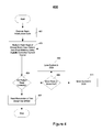
- FIG. 4 shows an exemplary embodiment of an algorithm 400 for addressing threshold voltage shifts of memory cells of an electronic product according to one embodiment.
- a flash read of a known worst case pattern stored in flash memory is performed using a digitally controlled current source.
- the process proceeds to 407 , and the remainder of the trim data stored in flash memory is read into SRAM. If the known pattern is not read correctly, then the process proceeds to 409 , and it is determined whether more ones or zeros failed in the comparison performed at 405 . If it is determined that more ones failed, then the digitally controlled current source is adjusted to provide less current at 413 . If it is determined that more zeros failed, then the digitally controlled current source is adjusted to provide more current at 411 .
- the algorithm that is used can involve a plurality of operations.
- the algorithm can direct a sweep of the complete range of possible reference levels (e.g., current values), and finding a passing value, guard band either side.
- the algorithm can direct a sweep of 0-30 uA, where passes are found at 9 ua, 9.5 ua, 10 ua, 10.5 ua and 11 ua. In this example, 10 ua may be chosen as it is the middle value with the most passes on either side.
- an algorithm can direct a sweep of the entire range of possible reference levels and use the reference level that provides the best sense margin or can terminate the search when the reference level that provides the first passing read is found such that time is saved.
- a method includes reading a pattern of data from a first plurality of memory cells, comparing the read of the pattern of data with a known pattern of data, using a reference, and if the read of the pattern of data and the known pattern of data do not match, adjusting the reference to find a reference level that results in a matching of a read of the pattern of data from the first plurality of memory cells and the known pattern of data. Thereafter, trim sector data is read into a second plurality of memory cells using the adjusted reference level.
Landscapes
- Read Only Memory (AREA)
Abstract
Description
Claims (20)
Priority Applications (1)
| Application Number | Priority Date | Filing Date | Title |
|---|---|---|---|
| US13/011,706 US8345483B2 (en) | 2011-01-21 | 2011-01-21 | System and method for addressing threshold voltage shifts of memory cells in an electronic product |
Applications Claiming Priority (1)
| Application Number | Priority Date | Filing Date | Title |
|---|---|---|---|
| US13/011,706 US8345483B2 (en) | 2011-01-21 | 2011-01-21 | System and method for addressing threshold voltage shifts of memory cells in an electronic product |
Publications (2)
| Publication Number | Publication Date |
|---|---|
| US20120188820A1 US20120188820A1 (en) | 2012-07-26 |
| US8345483B2 true US8345483B2 (en) | 2013-01-01 |
Family
ID=46544100
Family Applications (1)
| Application Number | Title | Priority Date | Filing Date |
|---|---|---|---|
| US13/011,706 Active 2031-06-30 US8345483B2 (en) | 2011-01-21 | 2011-01-21 | System and method for addressing threshold voltage shifts of memory cells in an electronic product |
Country Status (1)
| Country | Link |
|---|---|
| US (1) | US8345483B2 (en) |
Cited By (1)
| Publication number | Priority date | Publication date | Assignee | Title |
|---|---|---|---|---|
| US9691980B1 (en) * | 2016-08-18 | 2017-06-27 | Winbond Electronics Corp. | Method for forming memory device |
Families Citing this family (6)
| Publication number | Priority date | Publication date | Assignee | Title |
|---|---|---|---|---|
| US20130006896A1 (en) * | 2011-06-28 | 2013-01-03 | Seagate Technology Llc | Training Datasets for Memory Devices |
| US9025374B2 (en) | 2012-12-13 | 2015-05-05 | Sandisk Technologies Inc. | System and method to update read voltages in a non-volatile memory in response to tracking data |
| US10629247B2 (en) * | 2017-12-21 | 2020-04-21 | Western Digital Technologies, Inc. | Read threshold adjustment using reference data |
| CN114303200A (en) * | 2019-05-31 | 2022-04-08 | 美光科技公司 | Memory device and method for monitoring performance of memory device |
| US11442940B2 (en) * | 2020-03-03 | 2022-09-13 | Micron Technology, Inc. | Apparatuses and methods for on-memory pattern matching |
| US20240012576A1 (en) * | 2022-07-11 | 2024-01-11 | Micron Technology, Inc. | Toggling known patterns for reading memory cells in a memory device |
Citations (16)
| Publication number | Priority date | Publication date | Assignee | Title |
|---|---|---|---|---|
| US5142495A (en) * | 1989-03-10 | 1992-08-25 | Intel Corporation | Variable load for margin mode |
| US5966330A (en) * | 1998-04-30 | 1999-10-12 | Eon Silicon Devices, Inc. | Method and apparatus for measuring the threshold voltage of flash EEPROM memory cells being applied a variable control gate bias |
| US6118701A (en) * | 1998-05-19 | 2000-09-12 | Nec Corporation | Method and apparatus capable of trimming a nonvolatile semiconductor storage device without any superfluous pads or terminals |
| US6370060B2 (en) * | 2000-04-24 | 2002-04-09 | Sharp Kabushiki Kaisha | Semiconductor memory device |
| US6650570B2 (en) * | 2000-09-22 | 2003-11-18 | Kabushiki Kaisha Toshiba | Non-volatile semiconductor memory |
| US6826103B2 (en) * | 2002-10-30 | 2004-11-30 | Freescale Semiconductor, Inc. | Auto-tuneable reference circuit for flash EEPROM products |
| US7020037B2 (en) * | 2004-02-06 | 2006-03-28 | Sharp Kabushiki Kaisha | Nonvolatile semiconductor memory device |
| US7123514B2 (en) * | 2004-03-31 | 2006-10-17 | Nec Electronics Corporation | Memory device for improved reference current configuration |
| US7457178B2 (en) * | 2006-01-12 | 2008-11-25 | Sandisk Corporation | Trimming of analog voltages in flash memory devices |
| US7495955B2 (en) * | 2005-12-19 | 2009-02-24 | Nec Corporation | Nonvolative semiconductor memory device and operating method thereof |
| US7596037B2 (en) * | 2007-09-14 | 2009-09-29 | Silicon Storage Technology, Inc. | Independent bi-directional margin control per level and independently expandable reference cell levels for flash memory sensing |
| US7599220B2 (en) * | 2007-05-25 | 2009-10-06 | Macronix International Co., Ltd. | Charge trapping memory and accessing method thereof |
| US7729165B2 (en) * | 2007-03-29 | 2010-06-01 | Flashsilicon, Incorporation | Self-adaptive and self-calibrated multiple-level non-volatile memories |
| US7821836B2 (en) * | 2007-07-02 | 2010-10-26 | Samsung Electronics Co., Ltd. | Flash memory device and method in which trim information is stored in memory cell array |
| US7864588B2 (en) * | 2007-09-17 | 2011-01-04 | Spansion Israel Ltd. | Minimizing read disturb in an array flash cell |
| US8094493B2 (en) * | 2004-11-12 | 2012-01-10 | Macronix International Co., Ltd. | Memory devices and methods using improved reference cell trimming algorithms for accurate read operation window control |
-
2011
- 2011-01-21 US US13/011,706 patent/US8345483B2/en active Active
Patent Citations (16)
| Publication number | Priority date | Publication date | Assignee | Title |
|---|---|---|---|---|
| US5142495A (en) * | 1989-03-10 | 1992-08-25 | Intel Corporation | Variable load for margin mode |
| US5966330A (en) * | 1998-04-30 | 1999-10-12 | Eon Silicon Devices, Inc. | Method and apparatus for measuring the threshold voltage of flash EEPROM memory cells being applied a variable control gate bias |
| US6118701A (en) * | 1998-05-19 | 2000-09-12 | Nec Corporation | Method and apparatus capable of trimming a nonvolatile semiconductor storage device without any superfluous pads or terminals |
| US6370060B2 (en) * | 2000-04-24 | 2002-04-09 | Sharp Kabushiki Kaisha | Semiconductor memory device |
| US6650570B2 (en) * | 2000-09-22 | 2003-11-18 | Kabushiki Kaisha Toshiba | Non-volatile semiconductor memory |
| US6826103B2 (en) * | 2002-10-30 | 2004-11-30 | Freescale Semiconductor, Inc. | Auto-tuneable reference circuit for flash EEPROM products |
| US7020037B2 (en) * | 2004-02-06 | 2006-03-28 | Sharp Kabushiki Kaisha | Nonvolatile semiconductor memory device |
| US7123514B2 (en) * | 2004-03-31 | 2006-10-17 | Nec Electronics Corporation | Memory device for improved reference current configuration |
| US8094493B2 (en) * | 2004-11-12 | 2012-01-10 | Macronix International Co., Ltd. | Memory devices and methods using improved reference cell trimming algorithms for accurate read operation window control |
| US7495955B2 (en) * | 2005-12-19 | 2009-02-24 | Nec Corporation | Nonvolative semiconductor memory device and operating method thereof |
| US7457178B2 (en) * | 2006-01-12 | 2008-11-25 | Sandisk Corporation | Trimming of analog voltages in flash memory devices |
| US7729165B2 (en) * | 2007-03-29 | 2010-06-01 | Flashsilicon, Incorporation | Self-adaptive and self-calibrated multiple-level non-volatile memories |
| US7599220B2 (en) * | 2007-05-25 | 2009-10-06 | Macronix International Co., Ltd. | Charge trapping memory and accessing method thereof |
| US7821836B2 (en) * | 2007-07-02 | 2010-10-26 | Samsung Electronics Co., Ltd. | Flash memory device and method in which trim information is stored in memory cell array |
| US7596037B2 (en) * | 2007-09-14 | 2009-09-29 | Silicon Storage Technology, Inc. | Independent bi-directional margin control per level and independently expandable reference cell levels for flash memory sensing |
| US7864588B2 (en) * | 2007-09-17 | 2011-01-04 | Spansion Israel Ltd. | Minimizing read disturb in an array flash cell |
Cited By (1)
| Publication number | Priority date | Publication date | Assignee | Title |
|---|---|---|---|---|
| US9691980B1 (en) * | 2016-08-18 | 2017-06-27 | Winbond Electronics Corp. | Method for forming memory device |
Also Published As
| Publication number | Publication date |
|---|---|
| US20120188820A1 (en) | 2012-07-26 |
Similar Documents
| Publication | Publication Date | Title |
|---|---|---|
| US8345483B2 (en) | System and method for addressing threshold voltage shifts of memory cells in an electronic product | |
| US10061512B2 (en) | Data storage device and data writing method thereof | |
| US10068661B2 (en) | Post package repair (PPR) data in non-volatile memory | |
| JP5442789B2 (en) | Method, system, and computer readable code for testing flash memory | |
| US7142996B2 (en) | Operating voltage determination for an integrated circuit | |
| US9372750B2 (en) | Method and apparatus for non-volatile RAM error re-mapping | |
| US9514848B2 (en) | Solid state drive and associated error check and correction method | |
| US10018673B2 (en) | Semiconductor device and current control method of semiconductor device | |
| US10628265B2 (en) | Data backup method for performing post package repair (repair on system) operation | |
| US20170262337A1 (en) | Memory module repair system with failing component detection and method of operation thereof | |
| US20160155514A1 (en) | System and method of testing and identifying memory devices | |
| US9443566B2 (en) | Identification of a condition of a sector of memory cells in a non-volatile memory | |
| US20210026718A1 (en) | Memory controller and initialization method for use in data storage device | |
| US20090013192A1 (en) | Integrity check method applied to electronic device, and related circuit | |
| US7636828B2 (en) | Method for automatic adjustment of timing of double data rate interface | |
| CN110660436A (en) | Semiconductor memory device and memory controller | |
| US7334170B2 (en) | Method for resolving parameters of DRAM | |
| US7710802B2 (en) | Method for testing memory | |
| US20130080830A1 (en) | Setting data storage for semiconductor devices including memory devices and systems | |
| US9058863B2 (en) | Reference frequency setting method, memory controller and memory storage apparatus | |
| KR102024661B1 (en) | Nonvolatile memory device and method of reading data thereof | |
| US7512022B2 (en) | Non-volatile memory structure | |
| US20140223245A1 (en) | Volatile memory device and methods of operating and testing volatile memory device | |
| US20140317435A1 (en) | Electronic device and method for testing capacitors of motherboard of electronic device | |
| US20170235635A1 (en) | Solid state storage device and data processing method thereof |
Legal Events
| Date | Code | Title | Description |
|---|---|---|---|
| AS | Assignment |
Owner name: SPANSION LLC, CALIFORNIA Free format text: ASSIGNMENT OF ASSIGNORS INTEREST;ASSIGNORS:NEUMEYER, FREDERICK;YANCEY, GREG;SANCHEZ, PEDRO;AND OTHERS;SIGNING DATES FROM 20110207 TO 20110224;REEL/FRAME:025860/0368 |
|
| STCF | Information on status: patent grant |
Free format text: PATENTED CASE |
|
| AS | Assignment |
Owner name: MORGAN STANLEY SENIOR FUNDING, INC., NEW YORK Free format text: SECURITY INTEREST;ASSIGNORS:CYPRESS SEMICONDUCTOR CORPORATION;SPANSION LLC;REEL/FRAME:035240/0429 Effective date: 20150312 |
|
| AS | Assignment |
Owner name: CYPRESS SEMICONDUCTOR CORPORATION, CALIFORNIA Free format text: ASSIGNMENT OF ASSIGNORS INTEREST;ASSIGNOR:SPANSION, LLC;REEL/FRAME:036051/0786 Effective date: 20150601 |
|
| FPAY | Fee payment |
Year of fee payment: 4 |
|
| AS | Assignment |
Owner name: MUFG UNION BANK, N.A., CALIFORNIA Free format text: ASSIGNMENT AND ASSUMPTION OF SECURITY INTEREST IN INTELLECTUAL PROPERTY;ASSIGNOR:MORGAN STANLEY SENIOR FUNDING, INC.;REEL/FRAME:050896/0366 Effective date: 20190731 |
|
| MAFP | Maintenance fee payment |
Free format text: PAYMENT OF MAINTENANCE FEE, 8TH YEAR, LARGE ENTITY (ORIGINAL EVENT CODE: M1552); ENTITY STATUS OF PATENT OWNER: LARGE ENTITY Year of fee payment: 8 |
|
| AS | Assignment |
Owner name: MORGAN STANLEY SENIOR FUNDING, INC., NEW YORK Free format text: CORRECTIVE ASSIGNMENT TO CORRECT THE 8647899 PREVIOUSLY RECORDED ON REEL 035240 FRAME 0429. ASSIGNOR(S) HEREBY CONFIRMS THE SECURITY INTERST;ASSIGNORS:CYPRESS SEMICONDUCTOR CORPORATION;SPANSION LLC;REEL/FRAME:058002/0470 Effective date: 20150312 |
|
| AS | Assignment |
Owner name: SPANSION LLC, CALIFORNIA Free format text: RELEASE BY SECURED PARTY;ASSIGNOR:MUFG UNION BANK, N.A.;REEL/FRAME:059410/0438 Effective date: 20200416 Owner name: CYPRESS SEMICONDUCTOR CORPORATION, CALIFORNIA Free format text: RELEASE BY SECURED PARTY;ASSIGNOR:MUFG UNION BANK, N.A.;REEL/FRAME:059410/0438 Effective date: 20200416 |
|
| AS | Assignment |
Owner name: INFINEON TECHNOLOGIES LLC, CALIFORNIA Free format text: ASSIGNMENT OF ASSIGNORS INTEREST;ASSIGNOR:CYPRESS SEMICONDUCTOR CORPORATION;REEL/FRAME:059721/0467 Effective date: 20200315 |