US8406045B1 - Three terminal magnetic element - Google Patents

Three terminal magnetic element Download PDF

Info

Publication number
US8406045B1
US8406045B1 US13/009,818 US201113009818A US8406045B1 US 8406045 B1 US8406045 B1 US 8406045B1 US 201113009818 A US201113009818 A US 201113009818A US 8406045 B1 US8406045 B1 US 8406045B1
Authority
US
United States
Prior art keywords
layer
presetting
fixed layer
fixed
magnetization
Prior art date
Legal status (The legal status is an assumption and is not a legal conclusion. Google has not performed a legal analysis and makes no representation as to the accuracy of the status listed.)
Expired - Fee Related, expires
Application number
US13/009,818
Inventor
Eugene Youjun Chen
Dmytro Apalkov
Current Assignee (The listed assignees may be inaccurate. Google has not performed a legal analysis and makes no representation or warranty as to the accuracy of the list.)
Samsung Semiconductor Inc
Original Assignee
Grandis Inc
Priority date (The priority date is an assumption and is not a legal conclusion. Google has not performed a legal analysis and makes no representation as to the accuracy of the date listed.)
Filing date
Publication date
Application filed by Grandis Inc filed Critical Grandis Inc
Priority to US13/009,818 priority Critical patent/US8406045B1/en
Assigned to GRANDIS INC. reassignment GRANDIS INC. ASSIGNMENT OF ASSIGNORS INTEREST (SEE DOCUMENT FOR DETAILS). Assignors: APALKOV, DMYTRO, CHEN, EUGENE YOUJUN
Application granted granted Critical
Publication of US8406045B1 publication Critical patent/US8406045B1/en
Assigned to SAMSUNG SEMICONDUCTOR INC. reassignment SAMSUNG SEMICONDUCTOR INC. ASSIGNMENT OF ASSIGNORS INTEREST (SEE DOCUMENT FOR DETAILS). Assignors: GRANDIS, INC.
Expired - Fee Related legal-status Critical Current
Adjusted expiration legal-status Critical

Links

Images

Classifications

    • GPHYSICS
    • G11INFORMATION STORAGE
    • G11CSTATIC STORES
    • G11C11/00Digital stores characterised by the use of particular electric or magnetic storage elements; Storage elements therefor
    • G11C11/02Digital stores characterised by the use of particular electric or magnetic storage elements; Storage elements therefor using magnetic elements
    • G11C11/16Digital stores characterised by the use of particular electric or magnetic storage elements; Storage elements therefor using magnetic elements using elements in which the storage effect is based on magnetic spin effect
    • G11C11/161Digital stores characterised by the use of particular electric or magnetic storage elements; Storage elements therefor using magnetic elements using elements in which the storage effect is based on magnetic spin effect details concerning the memory cell structure, e.g. the layers of the ferromagnetic memory cell
    • GPHYSICS
    • G11INFORMATION STORAGE
    • G11CSTATIC STORES
    • G11C11/00Digital stores characterised by the use of particular electric or magnetic storage elements; Storage elements therefor
    • G11C11/02Digital stores characterised by the use of particular electric or magnetic storage elements; Storage elements therefor using magnetic elements
    • G11C11/16Digital stores characterised by the use of particular electric or magnetic storage elements; Storage elements therefor using magnetic elements using elements in which the storage effect is based on magnetic spin effect
    • G11C11/165Auxiliary circuits
    • G11C11/1675Writing or programming circuits or methods
    • HELECTRICITY
    • H10SEMICONDUCTOR DEVICES; ELECTRIC SOLID-STATE DEVICES NOT OTHERWISE PROVIDED FOR
    • H10NELECTRIC SOLID-STATE DEVICES NOT OTHERWISE PROVIDED FOR
    • H10N50/00Galvanomagnetic devices
    • H10N50/10Magnetoresistive devices

Definitions

  • This document relates to three terminal magnetic structures having at least one free ferromagnetic layer.
  • Magnetic memory devices use multilayer structures which have at least one ferromagnetic layer configured as a “free” layer whose magnetic direction can be changed by an external magnetic field or a control current.
  • Magnetic memory devices may be constructed using such multilayer structures where information is stored based on the magnetic direction of the free layer.
  • a spin valve which includes at least three layers: two ferromagnetic layers and a conducting layer between the two ferromagnetic layers.
  • a magnetic or magnetoresistive tunnel junction which includes at least three layers: two ferromagnetic layers and a thin layer of a non-magnetic insulator as a barrier layer between the two ferromagnetic layers. The insulator for the middle barrier layer functions as a tunnel barrier between the two ferromagnetic layers.
  • the thickness of the insulator is sufficiently thin, e.g., a few nanometers or less, electrons in the two ferromagnetic layers can tunnel or “penetrate” through the thin layer of the insulator due to a tunneling effect under a bias voltage applied to the two ferromagnetic layers across the barrier layer.
  • the resistance to the electrical current across the MTJ or SV structures varies with the relative direction of the magnetizations in the two ferromagnetic layers.
  • the resistance across the MTJ or SV structures is at a minimum value RP.
  • the resistance across the MTJ or SV is at a maximum value RAP.
  • the magnitude of this effect is commonly characterized by the tunneling magnetoresistance (TMR) in MTJs or magnetoresistance (MR) in SVs defined as (R AP ⁇ R P )/R P .
  • This document discloses techniques, devices and systems that use magnetic elements that include at least a presetting fixed layer having a fixed layer magnetization fixed in a direction substantially perpendicular to the plane of presetting fixed layer; a fixed layer having a fixed layer magnetization fixed in a direction substantially in the plane of the fixed layer; a free layer between the presetting fixed layer and fixed layer having a free layer magnetization with in-plane anisotropy; a first nonmagnetic spacer layer between the presetting fixed layer and the free layer; a second nonmagnetic spacer layer between the free layer and the fixed layer; and circuitry configured to apply a presetting current pulse and a write current pulse during a write operation, wherein: the presetting current pulse includes a current between the presetting fixed layer and free layer that presets the magnetization of the free layer magnetization at some angle away from the easy axis direction utilizing a spin transfer torque, the write current pulse includes a current between the free layer and fixed layer that reverses the direction of the magnetization of the free layer utilizing a
  • This document further discloses techniques, devices and systems that use magnetic elements that include at least a presetting fixed layer having a fixed layer magnetization fixed in a direction substantially perpendicular to the plane of presetting fixed layer; a fixed layer having a fixed layer magnetization fixed in a direction substantially in the plane of the fixed layer; a free layer having a free layer magnetization with in-plane anisotropy; a nonmagnetic spacer layer between the presetting fixed layer and the free layer and between the fixed layer and the free layer wherein the fixed layer and presetting fixed layer are laterally separated; and circuitry configured to apply a presetting current pulse and a write current pulse during a write operation, wherein: the presetting current pulse includes a current between the presetting fixed layer and free layer that presets the magnetization of the free layer magnetization at some angle away from the easy axis direction utilizing a spin transfer torque, the write current pulse includes a current between the free layer and fixed layer that reverses the direction of the magnetization of the free layer utilizing a spin transfer torque, and
  • This document further discloses techniques, devices and systems that use magnetic elements that include at least a presetting fixed layer having a fixed layer magnetization fixed in a direction substantially in the plane of presetting fixed layer; a fixed layer having a fixed layer magnetization fixed substantially in a direction perpendicular to the plane of the fixed layer; a free layer between the presetting fixed layer and fixed layer having a free layer magnetization with an out of plane anisotropy, which overcomes demagnetizing energy; a first nonmagnetic spacer layer between the presetting fixed layer and the free layer; a second nonmagnetic spacer layer between the free layer and the fixed layer; and circuitry configured to apply a presetting current pulse and a write current pulse during a write operation, wherein: the presetting current pulse includes a current between the presetting fixed layer and free layer that presets the magnetization of the free layer magnetization partially in-plane utilizing a spin transfer torque, the write current pulse includes a current between the free layer and fixed layer that reverses the direction of the magnetization of the free layer
  • This document further discloses techniques, devices and systems that use magnetic elements that include at least a presetting fixed layer having a fixed layer magnetization fixed substantially in a direction in the plane of presetting fixed layer; a fixed layer having a fixed layer magnetization fixed substantially in a direction perpendicular to the plane of the fixed layer; a free layer having a free layer magnetization with an out of plane anisotropy, which overcomes demagnetizing energy; a nonmagnetic spacer layer between the presetting fixed layer and the free layer and between the fixed layer and the free layer wherein the fixed layer and presetting fixed layer are laterally separated; and circuitry configured to apply a presetting current pulse and a write current pulse during a write operation, wherein: the presetting current pulse includes a current between the presetting fixed layer and free layer that presets the magnetization of the free layer magnetization partially in-plane utilizing a spin transfer torque, the write current pulse includes a current between the free layer and fixed layer that reverses the direction of the magnetization of the free layer utilizing a spin transfer
  • This document further discloses techniques, devices and systems that use magnetic elements that include at least a first contact; a first magnetic tunnel junction; a second contact; a second magnetic tunnel junction; and a third contact; wherein the first magnetic tunnel junction is disposed between the first contact and second contact, the second contact is disposed between the first magnetic tunnel junction and second magnetic tunnel junction, and the second magnetic tunnel junction is disposed between the second contact and third contact; and circuitry configured to apply a first write current pulse and second write current pulse, wherein: the first write current pulse includes a current between the first contact and second contact that reverses the state of the first magnetic tunnel junction utilizing a spin transfer torque; and the second write current pulse includes a current between the second contact and third contact that reverses the state of the first magnetic tunnel junction utilizing a spin transfer torque.
  • the use of three terminal magnetic elements may act to reduce the current pulse required to reverses the direction of the magnetization of the free layer utilizing a spin transfer torque, thus leading to lower power densities. In certain implementations, the use of three terminal magnetic elements may allow greater device densities.
  • FIG. 1A shows an example of a magnetic element in the form a spin valve.
  • FIG. 1B shows an example of a magnetic element in the form of a spin tunneling junction.
  • FIG. 2A depicts an example of a portion of a magnetic element having a free magnetic layer, a first pinned magnetic layer, and a pinned presetting layer, where the free magnetic layer has an in-plane anisotropy.
  • FIG. 2B depicts an example of a portion of a magnetic element having a free magnetic layer, a first pinned magnetic layer, and a pinned presetting layer, where the free magnetic layer has an out of plane anisotropy.
  • FIGS. 3A and 3C show two examples of a portion of a magnetic element having a free magnetic layer, a first pinned magnetic layer, and a pinned presetting layer.
  • FIGS. 3B and 3D show the application of drive voltage during write operation to magnetic elements having a free magnetic layer, a first pinned magnetic layer, and a pinned presetting layer.
  • FIG. 4 depicts an example of a portion of a magnetic element having a first magnetic tunnel junction and a second magnetic tunnel junction.
  • FIGS. 1A and 1B depict exemplary magnetic elements 10 and 10 ′.
  • the magnetic element 10 is a spin valve and includes an antiferromagnetic (AFM) layer 12 , a fixed layer 14 , a conductive spacer layer 16 and a free layer 18 .
  • Other layers, such as seed or capping layer can also be used.
  • the fixed layer 14 and the free layer 18 are ferromagnetic.
  • the free layer 18 is depicted as having a changeable magnetization 19 .
  • the magnetization of the free layer 18 is free to rotate, in response to an external magnetic field, a driving electric current, or a combination of both.
  • the conductive spacer layer 16 is nonmagnetic.
  • the AFM layer 12 is used to pin the magnetization of the fixed layer 14 in a particular direction. After post annealing, the ferromagnetic layer 14 is pinned with a fixed magnetization 15 .
  • top contact 20 and bottom contact 22 that can be used to drive current through the magnetic element 10 .
  • the magnetic element 10 ′ depicted in FIG. 1B is a magnetic tunneling junction.
  • the magnetic element 10 ′ includes an AFM layer 12 ′, a fixed layer 14 ′ having a fixed layer magnetization 15 ′, an insulating barrier layer 16 ′, a free layer 18 ′ having a changeable magnetization 19 ′.
  • the barrier layer 16 ′ is thin enough for electrons to tunnel through in a magnetic tunneling junction 10 ′.
  • MRAM Magnetic random access memory
  • one ferromagnetic layer is configured to have a fixed magnetic direction and the other ferromagnetic layer is a “free” layer whose magnetic direction can be changed to be either parallel or opposite to the fixed direction and thus operate as a recording layer.
  • Information is stored based on the relative magnetic direction of the two ferromagnetic layers on two sides of the barrier of the MTJ or SV. For example, binary bits “1” and “0” can be recorded as the parallel and anti-parallel orientations of the two ferromagnetic layers in the MTJ or SV.
  • Recording or writing a bit in the MTJ or SV can be achieved by switching the magnetization direction of the free layer, e.g., by a writing magnetic field generated by supplying currents to write lines disposed in a cross stripe shape, by a current flowing across the MTJ or SV based on the spin transfer effect, by a combination of applying both a writing magnetic field and a current, or by other means.
  • Magnetic random access memory devices utilizing a spin transfer effect in switching can be operated under a low switching current density, J c , below 10 7 A/cm 2 (e.g., around or below 10 6 A/cm 2 ) for practical device applications.
  • This low switching current density advantageously allows for formation of densely packed memory cells (e.g., sub-micron lateral dimensions) with a low current.
  • the reduction of spin-transfer switching current density J c can be critical for making MRAM devices featured by a fast operation speed, low power consumption, and a high spatial density of memory cells.
  • FIG. 2 a depicts one implementation of a magnetic element 100 having a presetting fixed layer.
  • the magnetic element 100 includes, in order, a presetting fixed layer 110 having a presetting fixed layer magnetization 111 , a nonmagnetic spacer layer 120 , a free layer 130 with magnetization 131 that can be written using spin transfer, a nonmagnetic spacer layer 140 , and a fixed layer 150 having a fixed layer magnetization 151 .
  • the presetting fixed layer 110 is provided with out of plane magnetization 111 .
  • the fixed layer 150 is provided with in-plane magnetization 151 .
  • the free layer 130 is provided with magnetization 131 with in-plane anisotropy.
  • Presetting fixed layer 110 , free layer 130 , and/or fixed layer 150 can include magnetic materials multilayered with nonmagnetic or oxide layers, in which the magnetic sublayers can be antiferro-magnetically or ferro-magnetically coupled.
  • Nonmagnetic spacer layer 120 and nonmagnetic spacer layer 140 can include insulating layers such as Al 2 O 3 , MgO, TiO, TaO, and other oxides.
  • Nonmagnetic spacer layer 120 and nonmagnetic spacer layer 140 can include conducting layers such as Cu.
  • An antiferromagnetic layer can be included to pin the magnetization of the presetting fixed layer magnetization 111 in a desired direction after post annealing.
  • An antiferromagnetic layer can be included to pin the magnetization of the fixed layer magnetization 151 in a desired direction after post annealing.
  • a capping layer can be included above fixed layer 150 .
  • a seed layer can be included under fixed layer 110 .
  • the magnetization 131 of free layer 130 is preset at an angle away from the easy axis direction with a presetting current utilizing a spin transfer torque, applied through electrodes described below.
  • a write current is applied between free layer 130 and fixed layer 150 to reverse the in-plane direction of magnetization 131 of free layer 130 .
  • FIG. 2 b depicts another implementation of a magnetic element 100 ′ having a presetting fixed layer.
  • the magnetic element 100 ′ includes, in order, a presetting fixed layer 110 ′ having a presetting fixed layer magnetization 111 ′, a nonmagnetic spacer layer 120 ′, a free layer 130 ′ with magnetization 131 ′ that can be written using spin transfer, a nonmagnetic spacer layer 140 ′, and a fixed layer 150 ′ having a fixed layer magnetization 151 ′.
  • the presetting fixed layer 110 ′ is provided with in-plane magnetization 111 ′.
  • the fixed layer 150 ′ is provided with out of plane magnetization 151 ′.
  • the free layer 130 ′ is provided with magnetization 131 ′ with out of plane anisotropy, which is higher than the demagnetizing energy.
  • Presetting fixed layer 110 ′, free layer 130 ′, and/or fixed layer 150 ′ can include magnetic materials multilayered with nonmagnetic or oxide layers, in which the magnetic sublayers can be antiferro-magnetically or ferro-magnetically coupled.
  • Nonmagnetic spacer layer 120 ′ and nonmagnetic spacer layer 140 ′ can include insulating layers such as Al 2 O 3 , MgO, TiO, TaO, and other oxides.
  • Nonmagnetic spacer layer 120 ′ and nonmagnetic spacer layer 140 ′ can include conducting layers such as Cu.
  • An antiferromagnetic layer can be included to pin the magnetization of the presetting fixed layer magnetization 111 ′ in a desired direction after post annealing.
  • An antiferromagnetic layer can be included to pin the magnetization of the fixed layer magnetization 151 ′ in a desired direction after post annealing.
  • a capping layer can be included above fixed layer 150 ′.
  • a seed layer can be included under fixed layer 110 ′.
  • the magnetization 131 ′ of free layer 130 ′ is preset partially in-plane with a presetting current utilizing a spin transfer torque, applied through electrodes described below.
  • a write current is applied between free layer 130 ′ and fixed layer 150 ′ to reverse the direction of magnetization 131 ′ of free layer 130 ′.
  • FIG. 3 a depicts an implementation of device 100 , a magnetic element 200 having a presetting fixed layer. While FIG. 3 a depicts a contacting structure implementing device 100 , the contacting structure could also be used to implement device 100 ′.
  • the magnetic element 200 includes, in order, a presetting fixed layer 210 having a presetting fixed layer magnetization, a nonmagnetic spacer layer 220 , a free layer 230 with magnetization that can be written using spin transfer, a nonmagnetic spacer layer 240 , and a fixed layer 250 having a fixed layer magnetization.
  • the presetting fixed layer 210 is provided with out of plane magnetization.
  • the fixed layer 250 is provided with in-plane magnetization.
  • the free layer 230 is provided with magnetization with in-plane anisotropy.
  • presetting fixed layer 210 , free layer 230 , and fixed layer 250 are fabricated with different lateral dimensions so as to allow selective electrical contact to each layer.
  • Electrical contacts 280 , 270 , and 260 are made to presetting fixed layer 210 , free layer 230 , and fixed layer 250 respectively.
  • electrical contact 280 can be made to the same side of presetting fixed layer 210 as the nonmagnetic spacer layer 220
  • electrical contact 270 can be made to the same side of free layer 230 as non-magnetic spacer layer 240
  • electrical contact 260 is made to the opposite side of fixed layer 250 from non-magnetic spacer layer 240 .
  • Electrical contact 280 can also be made to the opposite side of presetting fixed layer 210 as nonmagnetic spacer layer 220 .
  • Magnetic element 200 can be fabricated using selective deposition and etching techniques. For example, presetting fixed layer is deposited on a substrate, which may include a seed layer, followed by sequential deposition of layers nonmagnetic spacer layer 220 , free layer 230 , nonmagnetic spacer layer 240 , and fixed layer 250 . A capping layer may be deposited on fixed layer 250 . A mask and etch step is used to selectively remove portions of fixed layer 250 and nonmagnetic spacer layer 240 , stopping at free layer 230 . A second mask and etch step is used to selectively remove portions of free layer 230 and nonmagnetic spacer layer 220 , stopping at presetting fixed layer 210 . A dielectric is deposited.
  • a mask, etch, and metallization step is used to selectively expose a portion of presetting fixed layer 210 and deposit a contacting electrode 280 .
  • a mask, etch, and metallization step is used to selectively expose a portion of free layer 230 and deposit a contacting electrode 270 .
  • a mask, etch, and metallization step is used to selectively expose a portion of fixed layer 250 and deposit a contacting electrode 260 .
  • the magnetization of free layer 230 is preset away from its original direction with a presetting current utilizing a spin transfer torque by applying a voltage bias between electrical contacts 270 and 280 , shown as voltage pulse 285 in FIG. 3( b ).
  • the presetting current can pass through the presetting fixed layer 210 and free layer 230 , but not the fixed layer 250 .
  • a write current is applied between free layer 230 and fixed layer 250 to reverse the in-plane direction of magnetization of free layer 230 by applying a voltage bias between electrical contacts 260 and 270 , shown as voltage pulse 265 in FIG. 3( b ).
  • the write current can pass through fixed layer 250 and free layer 230 , but not the presetting fixed layer 210 .
  • the magnitude of the voltage pulse 285 can be less than the magnitude of the voltage pulse 265 .
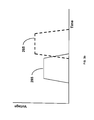
  • FIG. 3 c depicts an implementation of device 100 , a magnetic element 300 having a presetting fixed layer. While FIG. 3 c depicts a contacting structure implementing device 100 , the contacting structure could also be used to implement device 100 ′.
  • the magnetic element 300 includes a presetting fixed layer 310 having a presetting fixed layer magnetization, a free layer 330 with magnetization that can be written using spin transfer, a nonmagnetic spacer layer 340 , and a fixed layer 350 having a fixed layer magnetization.
  • Fixed layer 350 and presetting fixed layer 310 are adjacent laterally on the nonmagnetic spacer layer 340 (rather than stacked as in FIG. 3 a ) such that nonmagnetic spacer layer 340 lies between the free layer 330 and fixed layer 350 and also lies between the free layer 330 and presetting fixed layer 310 .
  • Fixed layer 350 and presetting fixed layer 310 can be spaced apart laterally, e.g., by a dielectric material.
  • the presetting fixed layer 310 is provided with out of plane magnetization.
  • the fixed layer 350 is provided with in-plane magnetization.
  • the free layer 330 is provided with magnetization with in-plane anisotropy.
  • presetting fixed layer 310 , free layer 330 , and fixed layer 350 are fabricated so as to allow selective electrical contact to each layer.
  • Electrical contacts 380 , 370 , and 360 are made to presetting fixed layer 310 , free layer 330 , and fixed layer 350 respectively.
  • electrical contact 380 can be made to the opposite side of presetting fixed layer 310 as the nonmagnetic spacer layer 340
  • electrical contact 360 is made to the opposite side of fixed layer 350 from nonmagnetic spacer layer 340
  • electrical contact 370 can be made to the opposite side of free layer 330 as nonmagnetic spacer layer 340 .
  • Magnetic element 300 can be fabricated using selective deposition and etching techniques.
  • the electrode 370 can be deposited on a substrate, and free layer 330 is deposited on the electrode 370 (a seed layer may be deposited on the electrode before free layer 330 ), followed by sequential deposition of nonmagnetic spacer layer 340 , and fixed layer 350 .
  • a capping layer may be deposited on fixed layer 350 .
  • a mask and etch step is used to selectively remove portions of fixed layer 350 and nonmagnetic spacer layer 340 , and free layer 330 .
  • a second mask and etch step is used to selectively remove portions of fixed layer 350 , stopping at nonmagnetic spacer layer 340 .
  • a mask and metallization step is used to selectively deposit presetting fixed layer 310 over nonmagnetic spacer layer 340 , adjacent to fixed layer 350 .
  • a dielectric is deposited.
  • a mask, etch, and metallization step is used to selectively expose a portion of presetting fix layer 310 and deposit a contacting electrode 380 .
  • a mask, etch, and metallization step is used to selectively expose a portion of fixed layer 350 and deposit a contacting electrode 360 .
  • contacts 360 and 380 may be made at the same steps.
  • the magnetization of free layer 330 is preset at some angle away from the easy axis direction with a presetting current utilizing a spin transfer torque by applying a voltage bias between electrical contacts 370 and 380 , shown as voltage pulse 385 in FIG. 3( d ).
  • the presetting current can pass through the presetting fixed layer 310 and free layer 330 , but not the fixed layer 350 .
  • a write current is applied between free layer 330 and fixed layer 350 to reverse the in-plane direction of magnetization of free layer 330 by applying a voltage bias between electrical contacts 360 and 370 , shown as voltage pulse 365 in FIG. 3( d ).
  • the write current can pass through fixed layer 350 and free layer 330 , but not the presetting fixed layer 310 .
  • the magnitude of the voltage pulse 385 can be less than the magnitude of the voltage pulse 365 .
  • FIG. 4 depicts another implementation of a magnetic element.
  • the magnetic element 400 includes, in order, a bottom contact 410 , a first MTJ 420 that can be written using spin transfer, a middle contact 430 , a second MTJ 440 that can be written using spin transfer, and a top contact 450 .
  • the first MTJ 420 can include a single MTJ, including an insulating layer disposed between a pinned magnetic layer and a free magnetic layer.
  • the first MTJ 420 can include a dual MTJ, including a first pinned magnetic layer, a first insulating layer, a free magnetic layer, a second insulating layer, and a second pinned magnetic layer.
  • the first MTJ 420 can include a free layer comprising a single magnetic layer or magnetic materials multilayered with nonmagnetic or oxide layers, in which the magnetic sublayers can be antiferro-magnetically or ferro-magnetically coupled.
  • the second MTJ 440 can include a single MTJ, including an insulating layer disposed between a pinned magnetic layer and a free magnetic layer.
  • the first MTJ 440 can include a dual MTJ, including a first pinned magnetic layer, a first insulating layer, a free magnetic layer, a second insulating layer, and a second pinned magnetic layer.
  • An antiferromagnetic layer can be included to pin the magnetization of the fixed layer magnetization(s) of the first MTJ 440 .
  • the second MTJ 440 can include a free layer comprising a single magnetic layer or magnetic materials multilayered with nonmagnetic or oxide layers, in which the magnetic sublayers can be antiferro-magnetically or ferro-magnetically coupled.
  • the state of the first MTJ 420 is set utilizing a spin transfer torque by applying a voltage bias between electrical contacts 410 and 430 .
  • the state of the second MTJ 440 is set utilizing a spin transfer torque by applying a voltage bias between electrical contacts 430 and 450 .

Abstract

Techniques and magnetic devices associated with a magnetic element are described that includes a presetting fixed layer having a presetting fixed layer magnetization, a free layer having a changeable free layer magnetization, and a fixed layer having a fixed layer magnetization, where a presetting current pulse applied between the presetting fixed layer and free layer operates to preset the free layer magnetization in advance of a write pulse. Techniques and magnetic devices associated with a magnetic element are described that includes a first terminal, a first magnetic tunnel junction, a second terminal, a second magnetic tunnel junction, and a third terminal, where a current pulse applied between the first and second terminal operate to switch the state of the first magnetic tunnel junction and a current applied between the second and third terminal operate to switch the state of the second magnetic tunnel junction.

Description

GOVERNMENT FUNDING
This invention was made with U.S. Government support under Grant/Contract No. HR0011-09-C-0023 awarded by DARPA. The U.S. Government retains certain rights in this invention.
BACKGROUND
This document relates to three terminal magnetic structures having at least one free ferromagnetic layer.
Various magnetic devices use multilayer structures which have at least one ferromagnetic layer configured as a “free” layer whose magnetic direction can be changed by an external magnetic field or a control current. Magnetic memory devices may be constructed using such multilayer structures where information is stored based on the magnetic direction of the free layer.
One example for such a multilayer structure is a spin valve (SV) which includes at least three layers: two ferromagnetic layers and a conducting layer between the two ferromagnetic layers. Another example for such a multilayer structure is a magnetic or magnetoresistive tunnel junction (MTJ) which includes at least three layers: two ferromagnetic layers and a thin layer of a non-magnetic insulator as a barrier layer between the two ferromagnetic layers. The insulator for the middle barrier layer functions as a tunnel barrier between the two ferromagnetic layers. When the thickness of the insulator is sufficiently thin, e.g., a few nanometers or less, electrons in the two ferromagnetic layers can tunnel or “penetrate” through the thin layer of the insulator due to a tunneling effect under a bias voltage applied to the two ferromagnetic layers across the barrier layer.
Notably, the resistance to the electrical current across the MTJ or SV structures varies with the relative direction of the magnetizations in the two ferromagnetic layers. When the magnetizations of the two ferromagnetic layers are parallel to each other, the resistance across the MTJ or SV structures is at a minimum value RP. When the magnetizations of the two ferromagnetic layers are anti-parallel with each other, the resistance across the MTJ or SV is at a maximum value RAP. The magnitude of this effect is commonly characterized by the tunneling magnetoresistance (TMR) in MTJs or magnetoresistance (MR) in SVs defined as (RAP−RP)/RP.
SUMMARY
This document discloses techniques, devices and systems that use three terminal magnetic elements.
This document discloses techniques, devices and systems that use magnetic elements that include at least a presetting fixed layer having a fixed layer magnetization fixed in a direction substantially perpendicular to the plane of presetting fixed layer; a fixed layer having a fixed layer magnetization fixed in a direction substantially in the plane of the fixed layer; a free layer between the presetting fixed layer and fixed layer having a free layer magnetization with in-plane anisotropy; a first nonmagnetic spacer layer between the presetting fixed layer and the free layer; a second nonmagnetic spacer layer between the free layer and the fixed layer; and circuitry configured to apply a presetting current pulse and a write current pulse during a write operation, wherein: the presetting current pulse includes a current between the presetting fixed layer and free layer that presets the magnetization of the free layer magnetization at some angle away from the easy axis direction utilizing a spin transfer torque, the write current pulse includes a current between the free layer and fixed layer that reverses the direction of the magnetization of the free layer utilizing a spin transfer torque, and the write current pulse is applied sequentially after the beginning of the presetting current pulse and before the magnetization of the free layer relaxes back to be substantially parallel with the anisotropy of the free layer.
This document further discloses techniques, devices and systems that use magnetic elements that include at least a presetting fixed layer having a fixed layer magnetization fixed in a direction substantially perpendicular to the plane of presetting fixed layer; a fixed layer having a fixed layer magnetization fixed in a direction substantially in the plane of the fixed layer; a free layer having a free layer magnetization with in-plane anisotropy; a nonmagnetic spacer layer between the presetting fixed layer and the free layer and between the fixed layer and the free layer wherein the fixed layer and presetting fixed layer are laterally separated; and circuitry configured to apply a presetting current pulse and a write current pulse during a write operation, wherein: the presetting current pulse includes a current between the presetting fixed layer and free layer that presets the magnetization of the free layer magnetization at some angle away from the easy axis direction utilizing a spin transfer torque, the write current pulse includes a current between the free layer and fixed layer that reverses the direction of the magnetization of the free layer utilizing a spin transfer torque, and the write current pulse is applied sequentially after the beginning of the presetting current pulse and before the magnetization of the free layer relaxes back to be substantially parallel with the anisotropy of the free layer.
This document further discloses techniques, devices and systems that use magnetic elements that include at least a presetting fixed layer having a fixed layer magnetization fixed in a direction substantially in the plane of presetting fixed layer; a fixed layer having a fixed layer magnetization fixed substantially in a direction perpendicular to the plane of the fixed layer; a free layer between the presetting fixed layer and fixed layer having a free layer magnetization with an out of plane anisotropy, which overcomes demagnetizing energy; a first nonmagnetic spacer layer between the presetting fixed layer and the free layer; a second nonmagnetic spacer layer between the free layer and the fixed layer; and circuitry configured to apply a presetting current pulse and a write current pulse during a write operation, wherein: the presetting current pulse includes a current between the presetting fixed layer and free layer that presets the magnetization of the free layer magnetization partially in-plane utilizing a spin transfer torque, the write current pulse includes a current between the free layer and fixed layer that reverses the direction of the magnetization of the free layer utilizing a spin transfer torque, and the write current pulse is applied sequentially after the beginning of the presetting current pulse and before the magnetization of the free layer relaxes back to be substantially parallel with the anisotropy easy axis of the free layer.
This document further discloses techniques, devices and systems that use magnetic elements that include at least a presetting fixed layer having a fixed layer magnetization fixed substantially in a direction in the plane of presetting fixed layer; a fixed layer having a fixed layer magnetization fixed substantially in a direction perpendicular to the plane of the fixed layer; a free layer having a free layer magnetization with an out of plane anisotropy, which overcomes demagnetizing energy; a nonmagnetic spacer layer between the presetting fixed layer and the free layer and between the fixed layer and the free layer wherein the fixed layer and presetting fixed layer are laterally separated; and circuitry configured to apply a presetting current pulse and a write current pulse during a write operation, wherein: the presetting current pulse includes a current between the presetting fixed layer and free layer that presets the magnetization of the free layer magnetization partially in-plane utilizing a spin transfer torque, the write current pulse includes a current between the free layer and fixed layer that reverses the direction of the magnetization of the free layer utilizing a spin transfer torque, and the write current pulse is applied sequentially after the beginning of the presetting current pulse and before the magnetization of the free layer relaxes back to be substantially parallel with the anisotropy easy axis of the free layer.
This document further discloses techniques, devices and systems that use magnetic elements that include at least a first contact; a first magnetic tunnel junction; a second contact; a second magnetic tunnel junction; and a third contact; wherein the first magnetic tunnel junction is disposed between the first contact and second contact, the second contact is disposed between the first magnetic tunnel junction and second magnetic tunnel junction, and the second magnetic tunnel junction is disposed between the second contact and third contact; and circuitry configured to apply a first write current pulse and second write current pulse, wherein: the first write current pulse includes a current between the first contact and second contact that reverses the state of the first magnetic tunnel junction utilizing a spin transfer torque; and the second write current pulse includes a current between the second contact and third contact that reverses the state of the first magnetic tunnel junction utilizing a spin transfer torque.
In certain implementations, the use of three terminal magnetic elements may act to reduce the current pulse required to reverses the direction of the magnetization of the free layer utilizing a spin transfer torque, thus leading to lower power densities. In certain implementations, the use of three terminal magnetic elements may allow greater device densities.
These and other implementations are described in greater detail in the drawings, the description and the claims.
BRIEF DESCRIPTION OF THE DRAWINGS
FIG. 1A shows an example of a magnetic element in the form a spin valve.
FIG. 1B shows an example of a magnetic element in the form of a spin tunneling junction.
FIG. 2A depicts an example of a portion of a magnetic element having a free magnetic layer, a first pinned magnetic layer, and a pinned presetting layer, where the free magnetic layer has an in-plane anisotropy.
FIG. 2B depicts an example of a portion of a magnetic element having a free magnetic layer, a first pinned magnetic layer, and a pinned presetting layer, where the free magnetic layer has an out of plane anisotropy.
FIGS. 3A and 3C show two examples of a portion of a magnetic element having a free magnetic layer, a first pinned magnetic layer, and a pinned presetting layer.
FIGS. 3B and 3D show the application of drive voltage during write operation to magnetic elements having a free magnetic layer, a first pinned magnetic layer, and a pinned presetting layer.
FIG. 4 depicts an example of a portion of a magnetic element having a first magnetic tunnel junction and a second magnetic tunnel junction.
DETAILED DESCRIPTION
FIGS. 1A and 1B depict exemplary magnetic elements 10 and 10′. The magnetic element 10 is a spin valve and includes an antiferromagnetic (AFM) layer 12, a fixed layer 14, a conductive spacer layer 16 and a free layer 18. Other layers, such as seed or capping layer can also be used. The fixed layer 14 and the free layer 18 are ferromagnetic. The free layer 18 is depicted as having a changeable magnetization 19. The magnetization of the free layer 18 is free to rotate, in response to an external magnetic field, a driving electric current, or a combination of both. The conductive spacer layer 16 is nonmagnetic. The AFM layer 12 is used to pin the magnetization of the fixed layer 14 in a particular direction. After post annealing, the ferromagnetic layer 14 is pinned with a fixed magnetization 15. Also depicted are top contact 20 and bottom contact 22 that can be used to drive current through the magnetic element 10.
The magnetic element 10′ depicted in FIG. 1B is a magnetic tunneling junction. The magnetic element 10′ includes an AFM layer 12′, a fixed layer 14′ having a fixed layer magnetization 15′, an insulating barrier layer 16′, a free layer 18′ having a changeable magnetization 19′. The barrier layer 16′ is thin enough for electrons to tunnel through in a magnetic tunneling junction 10′.
The relationship between the resistance to the current flowing across the MTJ or SV and the relative magnetic direction between the two ferromagnetic layers in the TMR or MR effect can be used for nonvolatile magnetic memory devices to store information in the magnetic state of the magnetic element. Magnetic random access memory (MRAM) devices based on the TMR or MR effect, for example, can be an alternative of and compete with electronic RAM devices. In such devices, one ferromagnetic layer is configured to have a fixed magnetic direction and the other ferromagnetic layer is a “free” layer whose magnetic direction can be changed to be either parallel or opposite to the fixed direction and thus operate as a recording layer. Information is stored based on the relative magnetic direction of the two ferromagnetic layers on two sides of the barrier of the MTJ or SV. For example, binary bits “1” and “0” can be recorded as the parallel and anti-parallel orientations of the two ferromagnetic layers in the MTJ or SV. Recording or writing a bit in the MTJ or SV can be achieved by switching the magnetization direction of the free layer, e.g., by a writing magnetic field generated by supplying currents to write lines disposed in a cross stripe shape, by a current flowing across the MTJ or SV based on the spin transfer effect, by a combination of applying both a writing magnetic field and a current, or by other means.
Magnetic random access memory devices utilizing a spin transfer effect in switching can be operated under a low switching current density, Jc, below 107 A/cm2 (e.g., around or below 106 A/cm2) for practical device applications. This low switching current density advantageously allows for formation of densely packed memory cells (e.g., sub-micron lateral dimensions) with a low current. The reduction of spin-transfer switching current density Jc can be critical for making MRAM devices featured by a fast operation speed, low power consumption, and a high spatial density of memory cells.
FIG. 2 a depicts one implementation of a magnetic element 100 having a presetting fixed layer. The magnetic element 100 includes, in order, a presetting fixed layer 110 having a presetting fixed layer magnetization 111, a nonmagnetic spacer layer 120, a free layer 130 with magnetization 131 that can be written using spin transfer, a nonmagnetic spacer layer 140, and a fixed layer 150 having a fixed layer magnetization 151. The presetting fixed layer 110 is provided with out of plane magnetization 111. The fixed layer 150 is provided with in-plane magnetization 151. The free layer 130 is provided with magnetization 131 with in-plane anisotropy.
Presetting fixed layer 110, free layer 130, and/or fixed layer 150 can include magnetic materials multilayered with nonmagnetic or oxide layers, in which the magnetic sublayers can be antiferro-magnetically or ferro-magnetically coupled. Nonmagnetic spacer layer 120 and nonmagnetic spacer layer 140 can include insulating layers such as Al2O3, MgO, TiO, TaO, and other oxides. Nonmagnetic spacer layer 120 and nonmagnetic spacer layer 140 can include conducting layers such as Cu. An antiferromagnetic layer can be included to pin the magnetization of the presetting fixed layer magnetization 111 in a desired direction after post annealing. An antiferromagnetic layer can be included to pin the magnetization of the fixed layer magnetization 151 in a desired direction after post annealing. A capping layer can be included above fixed layer 150. Also, a seed layer can be included under fixed layer 110.
In some implementations, during operation the magnetization 131 of free layer 130 is preset at an angle away from the easy axis direction with a presetting current utilizing a spin transfer torque, applied through electrodes described below. Before the magnetization 131 of free layer 130 relaxes to be substantially parallel with the in-plane anisotropy easy axis, a write current is applied between free layer 130 and fixed layer 150 to reverse the in-plane direction of magnetization 131 of free layer 130. By presetting the magnetization 131 of free layer 130 partially out of plane with a presetting current, the device may have the advantage of a reduced current density required and faster switching for full magnetization reversal utilizing a spin transfer torque.
FIG. 2 b depicts another implementation of a magnetic element 100′ having a presetting fixed layer. The magnetic element 100′ includes, in order, a presetting fixed layer 110′ having a presetting fixed layer magnetization 111′, a nonmagnetic spacer layer 120′, a free layer 130′ with magnetization 131′ that can be written using spin transfer, a nonmagnetic spacer layer 140′, and a fixed layer 150′ having a fixed layer magnetization 151′. The presetting fixed layer 110′ is provided with in-plane magnetization 111′. The fixed layer 150′ is provided with out of plane magnetization 151′. The free layer 130′ is provided with magnetization 131′ with out of plane anisotropy, which is higher than the demagnetizing energy.
Presetting fixed layer 110′, free layer 130′, and/or fixed layer 150′ can include magnetic materials multilayered with nonmagnetic or oxide layers, in which the magnetic sublayers can be antiferro-magnetically or ferro-magnetically coupled. Nonmagnetic spacer layer 120′ and nonmagnetic spacer layer 140′ can include insulating layers such as Al2O3, MgO, TiO, TaO, and other oxides. Nonmagnetic spacer layer 120′ and nonmagnetic spacer layer 140′ can include conducting layers such as Cu. An antiferromagnetic layer can be included to pin the magnetization of the presetting fixed layer magnetization 111′ in a desired direction after post annealing. An antiferromagnetic layer can be included to pin the magnetization of the fixed layer magnetization 151′ in a desired direction after post annealing. A capping layer can be included above fixed layer 150′. Also, a seed layer can be included under fixed layer 110′.
In some implementations, during operation the magnetization 131′ of free layer 130′ is preset partially in-plane with a presetting current utilizing a spin transfer torque, applied through electrodes described below. Before the magnetization 131′ of free layer 130′ relaxes to be substantially parallel with the out of plane anisotropy easy axis, a write current is applied between free layer 130′ and fixed layer 150′ to reverse the direction of magnetization 131′ of free layer 130′. By presetting the magnetization 131′ of free layer 130′ partially in-plane with a presetting current, the device may have the advantage of a reduced current density required and faster switching for full magnetization reversal utilizing a spin transfer torque.
FIG. 3 a depicts an implementation of device 100, a magnetic element 200 having a presetting fixed layer. While FIG. 3 a depicts a contacting structure implementing device 100, the contacting structure could also be used to implement device 100′.
The magnetic element 200 includes, in order, a presetting fixed layer 210 having a presetting fixed layer magnetization, a nonmagnetic spacer layer 220, a free layer 230 with magnetization that can be written using spin transfer, a nonmagnetic spacer layer 240, and a fixed layer 250 having a fixed layer magnetization. The presetting fixed layer 210 is provided with out of plane magnetization. The fixed layer 250 is provided with in-plane magnetization. The free layer 230 is provided with magnetization with in-plane anisotropy.
In this implementation, presetting fixed layer 210, free layer 230, and fixed layer 250 are fabricated with different lateral dimensions so as to allow selective electrical contact to each layer. Electrical contacts 280, 270, and 260 are made to presetting fixed layer 210, free layer 230, and fixed layer 250 respectively. In particular, electrical contact 280 can be made to the same side of presetting fixed layer 210 as the nonmagnetic spacer layer 220, electrical contact 270 can be made to the same side of free layer 230 as non-magnetic spacer layer 240, and electrical contact 260 is made to the opposite side of fixed layer 250 from non-magnetic spacer layer 240. Electrical contact 280 can also be made to the opposite side of presetting fixed layer 210 as nonmagnetic spacer layer 220. Although the contacts 260, 270, 280 are illustrated as adjacent, this is not necessary.
Magnetic element 200 can be fabricated using selective deposition and etching techniques. For example, presetting fixed layer is deposited on a substrate, which may include a seed layer, followed by sequential deposition of layers nonmagnetic spacer layer 220, free layer 230, nonmagnetic spacer layer 240, and fixed layer 250. A capping layer may be deposited on fixed layer 250. A mask and etch step is used to selectively remove portions of fixed layer 250 and nonmagnetic spacer layer 240, stopping at free layer 230. A second mask and etch step is used to selectively remove portions of free layer 230 and nonmagnetic spacer layer 220, stopping at presetting fixed layer 210. A dielectric is deposited. A mask, etch, and metallization step is used to selectively expose a portion of presetting fixed layer 210 and deposit a contacting electrode 280. A mask, etch, and metallization step is used to selectively expose a portion of free layer 230 and deposit a contacting electrode 270. Finally, a mask, etch, and metallization step is used to selectively expose a portion of fixed layer 250 and deposit a contacting electrode 260.
In this implementation, during operation the magnetization of free layer 230 is preset away from its original direction with a presetting current utilizing a spin transfer torque by applying a voltage bias between electrical contacts 270 and 280, shown as voltage pulse 285 in FIG. 3( b). Thus, the presetting current can pass through the presetting fixed layer 210 and free layer 230, but not the fixed layer 250. Before the magnetization of free layer 230 relaxes to be substantially parallel with the in-plane anisotropy easy axis, a write current is applied between free layer 230 and fixed layer 250 to reverse the in-plane direction of magnetization of free layer 230 by applying a voltage bias between electrical contacts 260 and 270, shown as voltage pulse 265 in FIG. 3( b). Thus, the write current can pass through fixed layer 250 and free layer 230, but not the presetting fixed layer 210. The magnitude of the voltage pulse 285 can be less than the magnitude of the voltage pulse 265.
FIG. 3 c depicts an implementation of device 100, a magnetic element 300 having a presetting fixed layer. While FIG. 3 c depicts a contacting structure implementing device 100, the contacting structure could also be used to implement device 100′.
The magnetic element 300 includes a presetting fixed layer 310 having a presetting fixed layer magnetization, a free layer 330 with magnetization that can be written using spin transfer, a nonmagnetic spacer layer 340, and a fixed layer 350 having a fixed layer magnetization. Fixed layer 350 and presetting fixed layer 310 are adjacent laterally on the nonmagnetic spacer layer 340 (rather than stacked as in FIG. 3 a) such that nonmagnetic spacer layer 340 lies between the free layer 330 and fixed layer 350 and also lies between the free layer 330 and presetting fixed layer 310. Fixed layer 350 and presetting fixed layer 310 can be spaced apart laterally, e.g., by a dielectric material. The presetting fixed layer 310 is provided with out of plane magnetization. The fixed layer 350 is provided with in-plane magnetization. The free layer 330 is provided with magnetization with in-plane anisotropy.
In this implementation, presetting fixed layer 310, free layer 330, and fixed layer 350 are fabricated so as to allow selective electrical contact to each layer. Electrical contacts 380, 370, and 360 are made to presetting fixed layer 310, free layer 330, and fixed layer 350 respectively. In particular, electrical contact 380 can be made to the opposite side of presetting fixed layer 310 as the nonmagnetic spacer layer 340, electrical contact 360 is made to the opposite side of fixed layer 350 from nonmagnetic spacer layer 340, and electrical contact 370 can be made to the opposite side of free layer 330 as nonmagnetic spacer layer 340.
Magnetic element 300 can be fabricated using selective deposition and etching techniques. For example, the electrode 370 can be deposited on a substrate, and free layer 330 is deposited on the electrode 370 (a seed layer may be deposited on the electrode before free layer 330), followed by sequential deposition of nonmagnetic spacer layer 340, and fixed layer 350. A capping layer may be deposited on fixed layer 350. A mask and etch step is used to selectively remove portions of fixed layer 350 and nonmagnetic spacer layer 340, and free layer 330. A second mask and etch step is used to selectively remove portions of fixed layer 350, stopping at nonmagnetic spacer layer 340. A mask and metallization step is used to selectively deposit presetting fixed layer 310 over nonmagnetic spacer layer 340, adjacent to fixed layer 350. A dielectric is deposited. A mask, etch, and metallization step is used to selectively expose a portion of presetting fix layer 310 and deposit a contacting electrode 380. A mask, etch, and metallization step is used to selectively expose a portion of fixed layer 350 and deposit a contacting electrode 360. Alternatively, contacts 360 and 380 may be made at the same steps.
In this implementation, during operation the magnetization of free layer 330 is preset at some angle away from the easy axis direction with a presetting current utilizing a spin transfer torque by applying a voltage bias between electrical contacts 370 and 380, shown as voltage pulse 385 in FIG. 3( d). Thus, the presetting current can pass through the presetting fixed layer 310 and free layer 330, but not the fixed layer 350. Before the magnetization of free layer 330 relaxes to be substantially parallel with the in-plane anisotropy, a write current is applied between free layer 330 and fixed layer 350 to reverse the in-plane direction of magnetization of free layer 330 by applying a voltage bias between electrical contacts 360 and 370, shown as voltage pulse 365 in FIG. 3( d). Thus, the write current can pass through fixed layer 350 and free layer 330, but not the presetting fixed layer 310. The magnitude of the voltage pulse 385 can be less than the magnitude of the voltage pulse 365.
FIG. 4 depicts another implementation of a magnetic element. The magnetic element 400 includes, in order, a bottom contact 410, a first MTJ 420 that can be written using spin transfer, a middle contact 430, a second MTJ 440 that can be written using spin transfer, and a top contact 450. The first MTJ 420 can include a single MTJ, including an insulating layer disposed between a pinned magnetic layer and a free magnetic layer. The first MTJ 420 can include a dual MTJ, including a first pinned magnetic layer, a first insulating layer, a free magnetic layer, a second insulating layer, and a second pinned magnetic layer. An antiferromagnetic layer can be included to pin the magnetization of the fixed layer magnetization(s) of the first MTJ 420. The first MTJ 420 can include a free layer comprising a single magnetic layer or magnetic materials multilayered with nonmagnetic or oxide layers, in which the magnetic sublayers can be antiferro-magnetically or ferro-magnetically coupled. The second MTJ 440 can include a single MTJ, including an insulating layer disposed between a pinned magnetic layer and a free magnetic layer. The first MTJ 440 can include a dual MTJ, including a first pinned magnetic layer, a first insulating layer, a free magnetic layer, a second insulating layer, and a second pinned magnetic layer. An antiferromagnetic layer can be included to pin the magnetization of the fixed layer magnetization(s) of the first MTJ 440. The second MTJ 440 can include a free layer comprising a single magnetic layer or magnetic materials multilayered with nonmagnetic or oxide layers, in which the magnetic sublayers can be antiferro-magnetically or ferro-magnetically coupled.
In this implementation, during operation the state of the first MTJ 420 is set utilizing a spin transfer torque by applying a voltage bias between electrical contacts 410 and 430. In this implementation, during operation the state of the second MTJ 440 is set utilizing a spin transfer torque by applying a voltage bias between electrical contacts 430 and 450. The use of three terminal magnetic elements with a first and second MTJ where each MTJ is individually controllable utilizing a spin transfer torque may allow greater device densities.
While this document contains many specifics, these should not be construed as limitations on the scope of an invention or of what may be claimed, but rather as descriptions of features specific to particular embodiments of the invention. Certain features that are described in this document in the context of separate embodiments can also be implemented in combination in a single embodiment. Conversely, various features that are described in the context of a single embodiment can also be implemented in multiple embodiments separately or in any suitable subcombination. Moreover, although features may be described above as acting in certain combinations and even initially claimed as such, one or more features from a claimed combination can in some cases be excised from the combination, and the claimed combination may be directed to a subcombination or a variation of a subcombination.
Only a few implementations are disclosed. Variations and enhancements of the described implementations and other implementations can be made based on what is described and illustrated in this document.

Claims (14)

What is claimed is:
1. A magnetic memory device comprising
a magnetic element including:
a presetting fixed layer having a fixed layer magnetization fixed in a direction substantially perpendicular to a plane of the presetting fixed layer;
a fixed layer having a fixed layer magnetization fixed in a direction substantially in a plane of the fixed layer;
a free layer between the presetting fixed layer and fixed layer having a free layer magnetization with in-plane anisotropy;
a first nonmagnetic spacer layer between the presetting fixed layer and the free layer; and
a second nonmagnetic spacer layer between the free layer and the fixed layer; and
circuitry configured to apply a presetting current pulse and a write current pulse during a write operation,
wherein:
the presetting current pulse includes a current between the presetting fixed layer and free layer that presets the magnetization of the free layer magnetization at some angle away from an easy axis direction utilizing a spin transfer torque,
the write current pulse includes a current between the free layer and fixed layer that reverses direction of magnetization of the free layer utilizing a spin transfer torque, and
the circuitry is configured to apply the write current pulse sequentially after a beginning of the presetting current pulse and before the magnetization of the free layer relaxes back to be substantially parallel with the anisotropy of the free layer.
2. The magnetic memory device of claim 1 wherein the second nonmagnetic spacer layer is an insulator.
3. The magnetic memory device of claim 1 further comprising:
a first electrical contact to the presetting fixed layer;
a second electrical contact to the free layer;
a third electrical contact to the fixed layer;
wherein the circuitry is configured to provide the presetting pulse between the first electrical contact and second electrical contact and is configured to provide the write pulse between the second electrical contact and third electrical contact.
4. The magnetic memory device of claim 3 wherein the lateral dimensions of the presetting fixed layer, the free layer, and the fixed layer are different.
5. A magnetic memory device comprising
a magnetic element including:
a presetting fixed layer having a fixed layer magnetization fixed in a direction substantially perpendicular to a plane of presetting fixed layer;
a fixed layer having a fixed layer magnetization fixed in a direction substantially in a plane of the fixed layer;
a free layer having a free layer magnetization with in-plane anisotropy;
a nonmagnetic spacer layer between the presetting fixed layer and the free layer and between the fixed layer and the free layer wherein the fixed layer and presetting fixed layer are laterally separated;
and circuitry configured to apply a presetting current pulse and a write current pulse during a write operation, wherein:
the presetting current pulse includes a current between the presetting fixed layer and free layer that presets the magnetization of the free layer magnetization at some angle away from an easy axis direction utilizing a spin transfer torque,
the write current pulse includes a current between the free layer and fixed layer that reverses a direction of the magnetization of the free layer utilizing a spin transfer torque, and
the circuitry is configured to apply the write current pulse sequentially after a beginning of the presetting current pulse and before the magnetization of the free layer relaxes back to be substantially parallel with the anisotropy of the free layer.
6. The magnetic memory device of claim 5 wherein the nonmagnetic spacer layer is an insulator.
7. The magnetic memory device of claim 5 further comprising:
a first electrical contact to the presetting fixed layer;
a second electrical contact to the free layer;
a third electrical contact to the fixed layer;
wherein the circuitry is configured to provide the presetting pulse between the first electrical contact and second electrical contact and is configured to provide the write pulse between the second electrical contact and third electrical contact.
8. A magnetic memory device comprising
a magnetic element including:
a presetting fixed layer having a fixed layer magnetization fixed in a direction substantially in a plane of the presetting fixed layer;
a fixed layer having a fixed layer magnetization fixed substantially in a direction perpendicular to a plane of the fixed layer;
a free layer between the presetting fixed layer and fixed layer having a free layer magnetization with an out of plane anisotropy, which overcomes demagnetizing energy;
a first nonmagnetic spacer layer between the presetting fixed layer and the free layer;
a second nonmagnetic spacer layer between the free layer and the fixed layer; and
circuitry configured to apply a presetting current pulse and a write current pulse during a write operation, wherein:
the presetting current pulse includes a current between the presetting fixed layer and free layer that presets the magnetization of the free layer magnetization partially in-plane utilizing a spin transfer torque,
the write current pulse includes a current between the free layer and fixed layer that reverses the direction of the magnetization of the free layer utilizing a spin transfer torque, and
the circuitry is configured to apply the write current pulse sequentially after a beginning of the presetting current pulse and before the magnetization of the free layer relaxes back to be substantially parallel with the anisotropy easy axis of the free layer.
9. The magnetic memory device of claim 8 wherein the second nonmagnetic spacer layer is an insulator.
10. The magnetic memory device of claim 8 further comprising:
a first electrical contact to the presetting fixed layer;
a second electrical contact to the free layer;
a third electrical contact to the fixed layer;
wherein the circuitry is configured to provide the presetting pulse between the first electrical contact and second electrical contact and is configured to provide the write pulse between the second electrical contact and third electrical contact.
11. The magnetic memory device of claim 10 wherein the lateral dimensions of the presetting fixed layer, the free layer, and the fixed layer are different.
12. A magnetic memory device comprising
a magnetic element including:
a presetting fixed layer having a fixed layer magnetization fixed substantially in a direction in a plane of presetting fixed layer;
a fixed layer having a fixed layer magnetization fixed substantially in a direction perpendicular to a plane of the fixed layer;
a free layer having a free layer magnetization with an out of plane anisotropy, which overcomes demagnetizing energy;
a nonmagnetic spacer layer between the presetting fixed layer and the free layer and between the fixed layer and the free layer wherein the fixed layer and presetting fixed layer are laterally separated;
and circuitry configured to apply a presetting current pulse and a write current pulse during a write operation, wherein:
the presetting current pulse includes a current between the presetting fixed layer and free layer to preset the magnetization of the free layer magnetization partially in-plane utilizing a spin transfer torque,
the write current pulse includes a current between the free layer and fixed layer that reverses the direction of the magnetization of the free layer utilizing a spin transfer torque, and
the circuitry is configured to apply the write current pulse sequentially after a beginning of the presetting current pulse and before the magnetization of the free layer relaxes back to be substantially parallel with the anisotropy easy axis of the free layer.
13. The magnetic memory device of claim 12 wherein the nonmagnetic spacer layer is an insulator.
14. The magnetic memory device of claim 12 further comprising:
a first electrical contact to the presetting fixed layer;
a second electrical contact to the free layer;
a third electrical contact to the fixed layer;
wherein the circuitry is configured to provide the presetting pulse between the first electrical contact and second electrical contact and is configured to provide the write pulse between the second electrical contact and third electrical contact.
US13/009,818 2011-01-19 2011-01-19 Three terminal magnetic element Expired - Fee Related US8406045B1 (en)

Priority Applications (1)

Application Number Priority Date Filing Date Title
US13/009,818 US8406045B1 (en) 2011-01-19 2011-01-19 Three terminal magnetic element

Applications Claiming Priority (1)

Application Number Priority Date Filing Date Title
US13/009,818 US8406045B1 (en) 2011-01-19 2011-01-19 Three terminal magnetic element

Publications (1)

Publication Number Publication Date
US8406045B1 true US8406045B1 (en) 2013-03-26

Family

ID=47892334

Family Applications (1)

Application Number Title Priority Date Filing Date
US13/009,818 Expired - Fee Related US8406045B1 (en) 2011-01-19 2011-01-19 Three terminal magnetic element

Country Status (1)

Country Link
US (1) US8406045B1 (en)

Cited By (5)

* Cited by examiner, † Cited by third party
Publication number Priority date Publication date Assignee Title
US20140217487A1 (en) * 2013-01-05 2014-08-07 T3Memory, Inc. Stt-mram and method of manufacturing the same
US9373781B2 (en) 2013-11-12 2016-06-21 Samsung Electronics Co., Ltd. Dual perpendicular magnetic anisotropy magnetic junction usable in spin transfer torque magnetic random access memory applications
US20180166623A1 (en) * 2015-10-20 2018-06-14 Taiwan Semiconductor Manufacturing Co., Ltd. Magnetic tunnel junction with reduced damage
CN110416406A (en) * 2019-08-13 2019-11-05 上海新微技术研发中心有限公司 Magnetic memory device
US10852369B2 (en) * 2019-01-09 2020-12-01 Infineon Technologies Ag Stray field robust xMR sensor using perpendicular anisotropy

Citations (11)

* Cited by examiner, † Cited by third party
Publication number Priority date Publication date Assignee Title
US5695864A (en) 1995-09-28 1997-12-09 International Business Machines Corporation Electronic device using magnetic components
US6714445B2 (en) 2001-08-28 2004-03-30 Micron Technology, Inc Three terminal magnetic random access memory
US6917088B2 (en) 2002-07-05 2005-07-12 Hitachi, Ltd. Magneto-resistive devices
US7009877B1 (en) 2003-11-14 2006-03-07 Grandis, Inc. Three-terminal magnetostatically coupled spin transfer-based MRAM cell
US7486552B2 (en) * 2007-05-21 2009-02-03 Grandis, Inc. Method and system for providing a spin transfer device with improved switching characteristics
US7764539B2 (en) 2007-11-21 2010-07-27 Magic Technologies, Inc. Spin transfer MRAM device with separated CPP assisted writing
US7781231B2 (en) 2008-03-07 2010-08-24 Qualcomm Incorporated Method of forming a magnetic tunnel junction device
US7936598B2 (en) * 2009-04-28 2011-05-03 Seagate Technology Magnetic stack having assist layer
US8023316B2 (en) * 2008-09-29 2011-09-20 Seagate Technology Llc Magnetic tunnel junction with compensation element
US8054677B2 (en) * 2008-08-07 2011-11-08 Seagate Technology Llc Magnetic memory with strain-assisted exchange coupling switch
US8102703B2 (en) * 2009-07-14 2012-01-24 Crocus Technology Magnetic element with a fast spin transfer torque writing procedure

Patent Citations (11)

* Cited by examiner, † Cited by third party
Publication number Priority date Publication date Assignee Title
US5695864A (en) 1995-09-28 1997-12-09 International Business Machines Corporation Electronic device using magnetic components
US6714445B2 (en) 2001-08-28 2004-03-30 Micron Technology, Inc Three terminal magnetic random access memory
US6917088B2 (en) 2002-07-05 2005-07-12 Hitachi, Ltd. Magneto-resistive devices
US7009877B1 (en) 2003-11-14 2006-03-07 Grandis, Inc. Three-terminal magnetostatically coupled spin transfer-based MRAM cell
US7486552B2 (en) * 2007-05-21 2009-02-03 Grandis, Inc. Method and system for providing a spin transfer device with improved switching characteristics
US7764539B2 (en) 2007-11-21 2010-07-27 Magic Technologies, Inc. Spin transfer MRAM device with separated CPP assisted writing
US7781231B2 (en) 2008-03-07 2010-08-24 Qualcomm Incorporated Method of forming a magnetic tunnel junction device
US8054677B2 (en) * 2008-08-07 2011-11-08 Seagate Technology Llc Magnetic memory with strain-assisted exchange coupling switch
US8023316B2 (en) * 2008-09-29 2011-09-20 Seagate Technology Llc Magnetic tunnel junction with compensation element
US7936598B2 (en) * 2009-04-28 2011-05-03 Seagate Technology Magnetic stack having assist layer
US8102703B2 (en) * 2009-07-14 2012-01-24 Crocus Technology Magnetic element with a fast spin transfer torque writing procedure

Non-Patent Citations (1)

* Cited by examiner, † Cited by third party
Title
Braganca, Patrick et al., "A Three-Terminal Approach to Developing Spin-Torgue Written Magnetic Random Access Memory Cells", IEEE Transactions on Nanotechnology, Mar. 2009, pp. 190-195, vol. 8.

Cited By (9)

* Cited by examiner, † Cited by third party
Publication number Priority date Publication date Assignee Title
US20140217487A1 (en) * 2013-01-05 2014-08-07 T3Memory, Inc. Stt-mram and method of manufacturing the same
US9461243B2 (en) * 2013-01-05 2016-10-04 Yimin Guo STT-MRAM and method of manufacturing the same
US9373781B2 (en) 2013-11-12 2016-06-21 Samsung Electronics Co., Ltd. Dual perpendicular magnetic anisotropy magnetic junction usable in spin transfer torque magnetic random access memory applications
US20180166623A1 (en) * 2015-10-20 2018-06-14 Taiwan Semiconductor Manufacturing Co., Ltd. Magnetic tunnel junction with reduced damage
US10672975B2 (en) * 2015-10-20 2020-06-02 Taiwan Semiconductor Manufacturing Company, Ltd. Magnetic tunnel junction with reduced damage
US11145806B2 (en) 2015-10-20 2021-10-12 Taiwan Semiconductor Manufacturing Company, Ltd. Magnetic tunnel junction with reduced damage
US10852369B2 (en) * 2019-01-09 2020-12-01 Infineon Technologies Ag Stray field robust xMR sensor using perpendicular anisotropy
US11519977B2 (en) 2019-01-09 2022-12-06 Infineon Technologies Ag Stray field robust XMR sensor using perpendicular anisotropy
CN110416406A (en) * 2019-08-13 2019-11-05 上海新微技术研发中心有限公司 Magnetic memory device

Similar Documents

Publication Publication Date Title
US10734054B2 (en) Magnetic structure based on synthetic antiferromagnetic free layer and derivative SOT-MRAM
US9666793B2 (en) Method of manufacturing magnetoresistive element(s)
KR102353406B1 (en) Magnetic devices including magnetic junctions having tilted easy axes and enhanced damping programmable using spin orbit torque
US7577021B2 (en) Spin transfer MRAM device with separated CPP assisted writing
US10953319B2 (en) Spin transfer MRAM element having a voltage bias control
KR100713270B1 (en) Magnetic memory element utilizing spin transfer switching and storing multiple bits
JP5537791B2 (en) Manufacturing method of MTJ element
US7965543B2 (en) Method for reducing current density in a magnetoelectronic device
US8482968B2 (en) Non-volatile magnetic tunnel junction transistor
US9461243B2 (en) STT-MRAM and method of manufacturing the same
US9099188B2 (en) Magnetoresistive element
US20140269036A1 (en) Magnetic memory devices and methods of writing data to the same
JP2016225633A (en) Voltage-controlled magnetic anisotropy switching device using external ferromagnetic biasing film
US8625327B2 (en) Magnetic random access memory and initializing method for the same
KR20070106701A (en) Mjt elements with high spin polarization layers configured for spin-transfer switching and spintronics devices using the magnetic elements
US9741929B2 (en) Method of making a spin-transfer-torque magnetoresistive random access memory (STT-MRAM)
JP7102448B2 (en) Magnetic tunnel junction storage element with magnetic exchange coupling free layer
JP6434103B1 (en) Magnetic memory
JP2007201059A (en) Magnetic element, magnetic recording equipment, and writing method
US8848435B2 (en) Magnetic resistance memory apparatus having multi levels and method of driving the same
US8406045B1 (en) Three terminal magnetic element
JP2008294056A (en) Magnetic recording device
WO2016039696A1 (en) Magnetic element and method of fabrication thereof

Legal Events

Date Code Title Description
AS Assignment

Owner name: GRANDIS INC., CALIFORNIA

Free format text: ASSIGNMENT OF ASSIGNORS INTEREST;ASSIGNORS:CHEN, EUGENE YOUJUN;APALKOV, DMYTRO;REEL/FRAME:026153/0381

Effective date: 20110118

STCF Information on status: patent grant

Free format text: PATENTED CASE

AS Assignment

Owner name: SAMSUNG SEMICONDUCTOR INC., CALIFORNIA

Free format text: ASSIGNMENT OF ASSIGNORS INTEREST;ASSIGNOR:GRANDIS, INC.;REEL/FRAME:037958/0728

Effective date: 20160224

FPAY Fee payment

Year of fee payment: 4

FEPP Fee payment procedure

Free format text: MAINTENANCE FEE REMINDER MAILED (ORIGINAL EVENT CODE: REM.); ENTITY STATUS OF PATENT OWNER: LARGE ENTITY

LAPS Lapse for failure to pay maintenance fees

Free format text: PATENT EXPIRED FOR FAILURE TO PAY MAINTENANCE FEES (ORIGINAL EVENT CODE: EXP.); ENTITY STATUS OF PATENT OWNER: LARGE ENTITY

STCH Information on status: patent discontinuation

Free format text: PATENT EXPIRED DUE TO NONPAYMENT OF MAINTENANCE FEES UNDER 37 CFR 1.362

FP Lapsed due to failure to pay maintenance fee

Effective date: 20210326