US8420999B2 - Metal shield and housing for optical proximity sensor with increased resistance to mechanical deformation - Google Patents
Metal shield and housing for optical proximity sensor with increased resistance to mechanical deformation Download PDFInfo
- Publication number
- US8420999B2 US8420999B2 US12/463,361 US46336109A US8420999B2 US 8420999 B2 US8420999 B2 US 8420999B2 US 46336109 A US46336109 A US 46336109A US 8420999 B2 US8420999 B2 US 8420999B2
- Authority
- US
- United States
- Prior art keywords
- metal
- proximity sensor
- housing
- optical proximity
- shield
- Prior art date
- Legal status (The legal status is an assumption and is not a legal conclusion. Google has not performed a legal analysis and makes no representation as to the accuracy of the status listed.)
- Expired - Fee Related, expires
Links
Images


Classifications
-
- G—PHYSICS
- G01—MEASURING; TESTING
- G01V—GEOPHYSICS; GRAVITATIONAL MEASUREMENTS; DETECTING MASSES OR OBJECTS; TAGS
- G01V8/00—Prospecting or detecting by optical means
- G01V8/10—Detecting, e.g. by using light barriers
-
- G—PHYSICS
- G01—MEASURING; TESTING
- G01D—MEASURING NOT SPECIALLY ADAPTED FOR A SPECIFIC VARIABLE; ARRANGEMENTS FOR MEASURING TWO OR MORE VARIABLES NOT COVERED IN A SINGLE OTHER SUBCLASS; TARIFF METERING APPARATUS; MEASURING OR TESTING NOT OTHERWISE PROVIDED FOR
- G01D11/00—Component parts of measuring arrangements not specially adapted for a specific variable
- G01D11/24—Housings ; Casings for instruments
- G01D11/245—Housings for sensors
-
- Y—GENERAL TAGGING OF NEW TECHNOLOGICAL DEVELOPMENTS; GENERAL TAGGING OF CROSS-SECTIONAL TECHNOLOGIES SPANNING OVER SEVERAL SECTIONS OF THE IPC; TECHNICAL SUBJECTS COVERED BY FORMER USPC CROSS-REFERENCE ART COLLECTIONS [XRACs] AND DIGESTS
- Y10—TECHNICAL SUBJECTS COVERED BY FORMER USPC
- Y10T—TECHNICAL SUBJECTS COVERED BY FORMER US CLASSIFICATION
- Y10T29/00—Metal working
- Y10T29/49—Method of mechanical manufacture
Definitions
- Optical proximity sensors such as the AVAGO TECHLOGIESTM HSDL-9100 surface-mount proximity sensor and the AVAGO TECHLOGIESTM APDS-9101 integrated reflective sensor, are known in the art. Such sensors typically comprise an integrated high efficiency infrared emitter or light source and a corresponding photodiode or light detector.
- FIG. 1 there is shown a prior art optical proximity sensor 10 comprising infrared light emitter 20 , light emitter driving circuit 21 , light detector or photodiode 30 , light detector sensing circuit 31 , metal housing or shield 40 with apertures 41 and 42 , and object, to be sensed 50 .
- Light rays 22 emitted by emitter 20 and reflected from object 50 (which is in relatively close proximity to optical proximity sensor 10 ) are detected by photodiode 31 and thereby provide an indication that object 60 is close or near to sensor 10 .
- optical proximity sensor 10 further comprises metal housing or shield 40 formed of metal and comprising apertures 42 and 43 located over light emitter 20 and light detector 30 , respectively, such that at least a first portion of light 22 emitted by light detector 20 passes through aperture 43 , and at least a second portion of the first portion 22 of light reflected from object 50 in proximity to sensor 10 passes through aperture 42 for detection by light detector 20 .
- metal housing or shield 40 further comprises first and second modules 41 and 44 within which light emitter 20 and light detector 30 are disposed, respectively.
- the first and second modules 41 and 44 comprise adjoining optically opaque metal inner sidewalls 45 to provide optical isolation between first and second modules 41 and 44 .
- Sensors such as the HSDL-9100 generally include a metal shield, such as shield or housing 40 shown in FIG. 1 , to provide optical isolation between light emitter 20 and photodiode 30 so that undesired optical cross-talk between emitter 20 and detector 30 is minimized.
- a metal shield such as shield or housing 40 shown in FIG. 1
- FIG. 2 shows a prior art optical proximity sensor 10 with metal shield or housing 40 that, has been damaged during the process of preparing sensor 10 for mounting on a printed circuit board.
- Sensor 10 shown in FIG. 2 is a surface mount device or SMD, and comprises printed circuit board or PCB substrate 61 , which is configured to permit sensor 10 to be attached to an underlying PCB, not shown in FIG. 2 .
- top covers 43 and 44 of housing 40 have been bent upwardly during handling of sensor 10 by automated assembly machinery, resulting in optical proximity sensor 10 becoming unusable for its intended function or purpose as an SMD optical proximity sensor mounted on a printed circuit board. It is believed that sponge-like material on the assembly machinery engages and protrudes through one or both of apertures 41 and 42 but does not subsequently release adequately therefrom, resulting in the damage to top covers 43 and 44 shown in FIG. 1
- an optical proximity sensor comprising an infrared light emitter operably connected to and driven by a light emitter driving circuit, a light detector operably connected to and driven by a detector sensing circuit, a metal housing or shield formed of metal and comprising first and second apertures located over the light emitter and the light detector, respectively, such that at least a first portion of light emitted by the light detector passes through the first aperture, and at least a second portion of the first portion of light reflected from ah object of interest in proximity to the sensor passes through the second aperture for detection by the light detector, wherein the metal housing or shield further comprises first and second modules within which the light detector and light detector are disposed, respectively, the first and second modules comprising adjoining optically opaque metal inner sidewalls to provide optical isolation between the first and second modules, the first and second inner sidewalls further being separated from one another by at least one metal tab foldably disposed therebetween, the at least one metal tab being configured to transfer a vertical force applied to one end of one module to an opposite end of
- a method of forming a metal housing or shield for an optical proximity sensor comprising forming a fiat sheet of metal configured to be folded into the shield or housing, the flat-sheet of metal comprising a plurality of tabs extending outwardly therefrom, folding the flat sheet of metal into first and second modules configured to house a light emitter and a light detector therewithin, respectively, such that the first and second modules comprise adjoining optically opaque metal inner sidewalls to provide optical isolation therebetween, the first and second inner sidewalls further being separated from one another by the plurality of tabs foldably disposed therebetween, the tabs and first and second modules further being configured to translate a vertical force applied to one end of one of the modules to an opposite end of the other module.
- FIG. 1 shows a cross-sectional view of a prior art optical proximity sensor
- FIG. 2 shows a bottom perspective view of a prior art optical proximity sensor where the metal shield or housing has sustained undesired damage
- FIGS. 3( a ) through 3 ( d ) show top, side, end and perspective views, respectively, of an optical proximity sensor metal shield or housing according to one embodiment
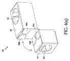
- FIGS. 4( a ) through 4 ( q ) show various steps of forming an optical proximity sensor metal shield or housing according to another embodiment
- FIG. 5 shows a top perspective view of tabs forming a portion of an optical proximity sensor shield or housing according to yet another embodiment.
- a metal shield or housing is provided for an optical proximity sensor or related type of sensor where the shield or housing is easily manufacturable at low cost but also possesses sufficient structurally robustness to resist undesired mechanical deformation during the manufacturing and assembly process.
- FIG. 1 shows a cross-sectional view of a prior art optical proximity sensor 10
- FIG. 2 shows a bottom perspective view of a prior art optical proximity sensor where a top portion of metal shield or housing 40 of sensor 10 has sustained undesired damage.
- housing or shield 40 shares certain similarities with prior art housing or shield illustrated in FIGS. 1 and 2 .
- housing or shield 40 of FIGS. 3( a ) through 3 ( d ) like housing or shield 40 of FIGS. 1 and 2 , includes apertures 42 and 42 , first and second modules 41 and 44 configured to receive light emitter 20 and light detector 30 , respectively, therein, and optically opaque sidewalls disposed between first and second modules 41 and 44 .
- housing or shield 40 shown in FIGS. 3( a ) through 3 ( d ) includes tabs 45 a through 45 d , which are disposed between the respective inner optically opaque sidewalls of first and second modules 41 and 44 .
- the purpose of tabs 45 ( a ) through 45 ( d ) is to convey any vertical force that might be acting on one of the modules laterally to the other adjoining module and thence downwardly to an underlying substrate to which the housing or shield is attached, such as a PCB substrate.
- vertical force 71 is acting upwardly on second module 44 .
- Vertical force 71 is translated or transferred laterally to first module 41 by way of forces 72 and 73 , which are transmitted between second module 44 and first module 41 through one or more of tabs 45 ( a ) through 45 ( d ), and thence downwardly (as indicated by force vector 74 ) to an underlying substrate (not shown in FIGS. 3( a ) through 3 ( d )).
- Such transfer and redirection of vertical forces acting on housing or shield 40 can also occur in the opposite direction, namely by having a vertical force acting initially on first module 41 transferred laterally to second module 44 and thence downwardly from second module 44 to an underlying substrate.
- FIGS. 4( a ) through 4 ( q ) show various steps of forming optical proximity sensor metal shield or housing 40 according to one embodiment.
- one method of forming metal housing or shield 40 for an optical proximity, sensor begins with providing a single contiguous flat sheet of metal 40 (see FIG. 4( a ) that has been cut and stamped to be folded ultimately into shield or housing 40 (see FIG. 4( q ). As shown In FIG.
- flat sheet of metal 40 initially comprises a plurality of tabs 45 ( a )- 45 ( d ), 46 ( a )- 46 ( b ), and 47 ( a )- 47 ( b ) extending outwardly therefrom, with precut or stamped apertures 42 and 43 , where all the features of initially flat sheet of metal 40 are disposed substantially in a single plane. It will be appreciated that such an initial configuration for flat sheet of metal 40 results in low manufacturing costs and relative ease and speed of subsequent manufacturing, wherein that is required to complete the formation of housing or shield 40 is to bend various portions thereof in predetermined directions and to predetermined positions. No welding, gluing, or other costly means of joining various portions of housing or shield 40 together are required.
- tabs 45 ( a ) through 45 ( d ) eventually wind up being disposed between modules 41 and 44 so that they can act as means for transferring forces between first module 41 and second module 44 , and vice versa, and that tabs 46 ( a ) and 46 ( b ), and 47 ( a ) and 47 ( b ), wind up forming the end sidewalls of first module 41 and second module 44 , respectively.
- housing or shield 40 In the embodiment of housing or shield 40 illustrated in FIGS. 3( a ) through 4 ( q ), a total of two upper tabs (i.e., upper tabs 45 ( a ) and 45 ( b ) foldably attached to second module 44 ) and two lower tabs (i.e., lower tabs 45 ( c ) and 45 ( d ) foldably attached to first module 41 ), for a total of four tabs, are disposed between first and second modules 41 and 44 . Contrariwise, in the embodiment of housing or shield 40 illustrated in FIG.
- the flat sheet of molar from which housing or shield 40 is formed may be stamped or cut using any of a number of different techniques know to those skilled in the art, such as laser cutting, melting with arc welders, mechanical abrasion or cutting, and so on.
- the metal from which housing or shield 40 is formed may be, by way of example, mild steel, stainless steel or nickel-plated steel stock.
- light emitter 20 and light emitter driving circuitry 21 may be mounted in first module 41
- light detector 30 and light sensing circuitry 31 may be mounted in second module 44
- a printed circuit, board substrate may then be disposed beneath housing or shield 40 and operably connected to circuits 21 and 31 to yield an operative proximity sensor 10 , which may then be incorporated info a portable electronic device such as a cellular telephone, a personal data assistant (PDA), a laptop computer, a notebook computer, or a computer
- PDA personal data assistant
Abstract
Description
Claims (20)
Priority Applications (3)
| Application Number | Priority Date | Filing Date | Title |
|---|---|---|---|
| US12/463,361 US8420999B2 (en) | 2009-05-08 | 2009-05-08 | Metal shield and housing for optical proximity sensor with increased resistance to mechanical deformation |
| DE102010028139.5A DE102010028139B4 (en) | 2009-05-08 | 2010-04-22 | Metallic shield and housing for an optical proximity sensor with increased resistance to unwanted mechanical deformation |
| JP2010108238A JP5480005B2 (en) | 2009-05-08 | 2010-05-10 | Optical proximity sensor metal shield and housing with increased resistance to undesirable mechanical deformation |
Applications Claiming Priority (1)
| Application Number | Priority Date | Filing Date | Title |
|---|---|---|---|
| US12/463,361 US8420999B2 (en) | 2009-05-08 | 2009-05-08 | Metal shield and housing for optical proximity sensor with increased resistance to mechanical deformation |
Publications (2)
| Publication Number | Publication Date |
|---|---|
| US20100282951A1 US20100282951A1 (en) | 2010-11-11 |
| US8420999B2 true US8420999B2 (en) | 2013-04-16 |
Family
ID=42932643
Family Applications (1)
| Application Number | Title | Priority Date | Filing Date |
|---|---|---|---|
| US12/463,361 Expired - Fee Related US8420999B2 (en) | 2009-05-08 | 2009-05-08 | Metal shield and housing for optical proximity sensor with increased resistance to mechanical deformation |
Country Status (3)
| Country | Link |
|---|---|
| US (1) | US8420999B2 (en) |
| JP (1) | JP5480005B2 (en) |
| DE (1) | DE102010028139B4 (en) |
Cited By (12)
| Publication number | Priority date | Publication date | Assignee | Title |
|---|---|---|---|---|
| US20110057108A1 (en) * | 2009-09-10 | 2011-03-10 | Avago Technologies Ecbu (Singapore) Pte. Ltd. | Compact Optical Proximity Sensor with Ball Grid Array and Windowed Substrate |
| US20110121181A1 (en) * | 2009-11-23 | 2011-05-26 | Avago Technologies Ecbu (Singapore) Pte. Ltd. | Infrared Proximity Sensor Package with Improved Crosstalk Isolation |
| US20110204233A1 (en) * | 2009-06-30 | 2011-08-25 | Avago Technologies Ecbu (Singapore) Pte. Ltd. | Infrared Attenuating or Blocking Layer in Optical Proximity Sensor |
| US20120160994A1 (en) * | 2010-12-27 | 2012-06-28 | Avago Technologies Ecbu Ip (Singapore) Pte. Ltd. | Housing for optical proximity sensor |
| US20120175506A1 (en) * | 2011-01-10 | 2012-07-12 | Apple, Inc. | Sheet and block for enhancing proximity sensor performance |
| US20120223231A1 (en) * | 2011-03-01 | 2012-09-06 | Lite-On Singapore Pte. Ltd. | Proximity sensor having electro-less plated shielding structure |
| US20130026350A1 (en) * | 2011-07-26 | 2013-01-31 | Avago Technologies Ecbu Ip (Singapore) Pte. Ltd. | Multi-directional proximity sensor |
| US8779361B2 (en) | 2009-06-30 | 2014-07-15 | Avago Technologies General Ip (Singapore) Pte. Ltd. | Optical proximity sensor package with molded infrared light rejection barrier and infrared pass components |
| US20140223734A1 (en) * | 2013-02-09 | 2014-08-14 | Lite-On Singapore Pte. Ltd. | Method of manufacturing proximity sensor |
| US9525093B2 (en) | 2009-06-30 | 2016-12-20 | Avago Technologies General Ip (Singapore) Pte. Ltd. | Infrared attenuating or blocking layer in optical proximity sensor |
| US9632209B2 (en) | 2015-03-25 | 2017-04-25 | Hana Microelectronics, Inc. | Proximity sensor with light blocking compound |
| US20200057158A1 (en) * | 2018-08-20 | 2020-02-20 | Lite-On Singapore Pte. Ltd. | Proximity sensor module with two sensors |
Families Citing this family (15)
| Publication number | Priority date | Publication date | Assignee | Title |
|---|---|---|---|---|
| US8217482B2 (en) * | 2007-12-21 | 2012-07-10 | Avago Technologies General Ip (Singapore) Pte. Ltd. | Infrared proximity sensor package with reduced crosstalk |
| US20100259766A1 (en) * | 2009-04-14 | 2010-10-14 | Intersil Americas Inc. | Optical sensors and methods for providing optical sensors |
| US8324602B2 (en) * | 2009-04-14 | 2012-12-04 | Intersil Americas Inc. | Optical sensors that reduce specular reflections |
| US8420999B2 (en) | 2009-05-08 | 2013-04-16 | Avago Technologies Ecbu Ip (Singapore) Pte. Ltd. | Metal shield and housing for optical proximity sensor with increased resistance to mechanical deformation |
| US8350216B2 (en) * | 2009-09-10 | 2013-01-08 | Avago Technologies Ecbu Ip (Singapore) Pte. Ltd. | Miniaturized optical proximity sensor |
| US8143608B2 (en) * | 2009-09-10 | 2012-03-27 | Avago Technologies Ecbu Ip (Singapore) Pte. Ltd. | Package-on-package (POP) optical proximity sensor |
| JP5365545B2 (en) * | 2010-02-25 | 2013-12-11 | 富士通オプティカルコンポーネンツ株式会社 | Optical device and optical device manufacturing method |
| JP4967065B2 (en) | 2011-02-24 | 2012-07-04 | 任天堂株式会社 | Image processing program, image processing apparatus, image processing system, and image processing method |
| AU2012203158B2 (en) * | 2011-06-08 | 2014-01-30 | Embertec Pty Ltd | Apparatus and method for shielding an IR detecting diode |
| JP5981183B2 (en) * | 2012-03-23 | 2016-08-31 | 矢崎総業株式会社 | Display device |
| US10165954B2 (en) | 2014-07-31 | 2019-01-01 | Salutron Inc. | Integrated sensor modules |
| TWI619959B (en) * | 2016-07-11 | 2018-04-01 | 光寶新加坡有限公司 | Sensing device and manufacturing method thereof |
| US11143551B2 (en) | 2018-05-18 | 2021-10-12 | Hana Microelectronics, Inc. | Proximity sensor with infrared ink coating |
| US11520074B2 (en) | 2018-09-14 | 2022-12-06 | Hana Microelectronics, Inc. | Proximity sensor with light blocking barrier comprising a gap having a cross-section with parallel walls between emitter and detector |
| US11567198B2 (en) | 2019-03-25 | 2023-01-31 | Hana Microelectronics Inc. | Proximity sensor with light inhibiting barrier comprising a gap having a cross-section with parallel walls substantially perpendicular to the top surface of an optically transmissive material |
Citations (69)
| Publication number | Priority date | Publication date | Assignee | Title |
|---|---|---|---|---|
| JPS63308973A (en) | 1987-06-11 | 1988-12-16 | Nec Corp | Manufacture of optical reflection type sensor |
| US5155777A (en) | 1991-06-26 | 1992-10-13 | International Business Machines Corporation | Scattered light blocking layer for optoelectronic receivers |
| US5367393A (en) | 1992-03-06 | 1994-11-22 | Seiko Epson Corporation | Electro-optical apparatus with metal light shield and conductor between color filters |
| US5675143A (en) | 1994-12-22 | 1997-10-07 | Optosys Ag | Proximity switch |
| US5811797A (en) | 1995-09-20 | 1998-09-22 | Sharp Kabushiki Kaisha | Photoreflective detector including a light emitting element and a light recieving element located at different distances from an object reflecting light from the emitting element |
| US6064062A (en) | 1998-06-02 | 2000-05-16 | Hewlett-Packard Company | Optical stray light baffle for image scanner |
| US6135816A (en) | 1998-04-27 | 2000-10-24 | Ddk Ltd. | Electrical connector having an improved construction for fixing shield plates to a receptacle connector |
| US6180881B1 (en) | 1998-05-05 | 2001-01-30 | Harlan Ruben Isaak | Chip stack and method of making same |
| US6364706B1 (en) | 1998-10-19 | 2002-04-02 | Molex Incorporated | Shielded electrical connector with flange support member |
| US20020172472A1 (en) | 2001-04-09 | 2002-11-21 | Steven Nelson | Optical attenuating underchip encapsulant |
| US6572410B1 (en) | 2002-02-20 | 2003-06-03 | Fci Americas Technology, Inc. | Connection header and shield |
| US6635955B2 (en) | 2000-11-15 | 2003-10-21 | Vishay Semiconductor Gmbh | Molded electronic component |
| US6674653B1 (en) | 1999-04-16 | 2004-01-06 | Agilent Technologies, Inc. | Shielding scheme for a circuit board |
| US20040065894A1 (en) | 2001-08-28 | 2004-04-08 | Takuma Hashimoto | Light emitting device using led |
| EP1455564A1 (en) | 2003-03-05 | 2004-09-08 | Sony Ericsson Mobile Communications AB | Electronic device provided with an EMI shield |
| US6885300B1 (en) | 2002-06-05 | 2005-04-26 | The Watt Stopper, Inc. | Broad field motion detector |
| US20050088900A1 (en) | 1998-09-25 | 2005-04-28 | Chan Tsiu C. | Stacked multi-component integrated circuit microprocessor |
| US20050110157A1 (en) | 2003-09-15 | 2005-05-26 | Rohm And Haas Electronic Materials, L.L.C. | Device package and method for the fabrication and testing thereof |
| US20060016994A1 (en) * | 2004-07-22 | 2006-01-26 | Suresh Basoor | System and method to prevent cross-talk between a transmitter and a receiver |
| US20060017069A1 (en) | 2002-02-18 | 2006-01-26 | Robert Bergmann | Electronic component with an adhesive layer and method for the production thereof |
| US20060022212A1 (en) | 1997-12-15 | 2006-02-02 | Osram Gmbh, A Germany Corporation | Surface mounting optoelectronic component and method for producing same |
| US20060022215A1 (en) | 2003-01-30 | 2006-02-02 | Karlheinz Arndt | Semiconductor component emitting and/or receiving electromagnetic radiation, and housing base for such a component |
| CN1743886A (en) | 2004-08-31 | 2006-03-08 | 安捷伦科技有限公司 | Compact optical transceiver module |
| US7026710B2 (en) | 2000-01-21 | 2006-04-11 | Texas Instruments Incorporated | Molded package for micromechanical devices and method of fabrication |
| US20060118807A1 (en) | 2004-12-08 | 2006-06-08 | Ives Fred H | Electronic microcircuit having internal light enhancement |
| US7172126B2 (en) | 1998-12-03 | 2007-02-06 | Metrologic Instruments, Inc. | Wireless automatic laser scanning bar code symbol reading system, wherein the RF-based transceiver chipsets within the wireless hand-supportable unit and base station thereof are automatically deactivated and said RF data communication link therebetween terminated when said system enters its power-saving sleep mode, and reactivated and re-established when re-entering its operational mode |
| US20070045524A1 (en) | 2003-06-23 | 2007-03-01 | Advanced Optical Technologies, Llc | Intelligent solid state lighting |
| US20070085157A1 (en) | 2005-09-30 | 2007-04-19 | Fadell Anthony M | Integrated proximity sensor and light sensor |
| US7229295B2 (en) | 2004-02-27 | 2007-06-12 | Finisar Corporation | Transceiver module having a dual segment lead frame connector |
| US7256483B2 (en) | 2004-10-28 | 2007-08-14 | Philips Lumileds Lighting Company, Llc | Package-integrated thin film LED |
| US7258264B2 (en) | 2004-02-27 | 2007-08-21 | Finisar Corporation | Methods for manufacturing optical modules using lead frame connectors |
| US7289142B2 (en) | 1997-07-15 | 2007-10-30 | Silverbrook Research Pty Ltd | Monolithic integrated circuit having a number of programmable processing elements |
| US20080006762A1 (en) | 2005-09-30 | 2008-01-10 | Fadell Anthony M | Integrated proximity sensor and light sensor |
| US20080011940A1 (en) | 2006-07-13 | 2008-01-17 | Jing Zhang | Remote control receiver device and ambient light photosensor device incorporated into a single composite assembly |
| US20080011939A1 (en) | 2006-07-13 | 2008-01-17 | Pak Hong Yee | Composite assembly that incorporates multiple devices that use different wavelengths of light and method for making same |
| US20080012033A1 (en) | 2004-05-31 | 2008-01-17 | Karlheinz Arndt | Optoelectronic Semiconductor Component and Housing Base for Such a Component |
| US20080049210A1 (en) | 2006-08-28 | 2008-02-28 | Sharp Kabushiki Kaisha | Range-finding sensor, and electronic device equipped with range-finding sensor |
| US20080116379A1 (en) | 2006-11-16 | 2008-05-22 | Pilkington North America | Multi-mode rain sensor |
| US20080118241A1 (en) | 2006-11-16 | 2008-05-22 | Tekolste Robert | Control of stray light in camera systems employing an optics stack and associated methods |
| US7387907B2 (en) | 2004-06-17 | 2008-06-17 | Taiwan Semiconductor Manufacturing Co., Ltd. | Image sensor with optical guard ring and fabrication method thereof |
| US7387033B2 (en) | 2005-06-17 | 2008-06-17 | Acellent Technologies, Inc. | Single-wire sensor/actuator network for structure health monitoring |
| US20080165115A1 (en) | 2007-01-05 | 2008-07-10 | Herz Scott M | Backlight and ambient light sensor system |
| US20080173963A1 (en) | 2007-01-24 | 2008-07-24 | Taiwan Semiconductor Manufacturing Company, Ltd. | Guard ring structure for improving crosstalk of backside illuminated image sensor |
| US20080197376A1 (en) | 2005-02-28 | 2008-08-21 | Braune Bert | Method for Producing an Optical, Radiation-Emitting Component and Optical, Radiation-Emitting Component |
| US20080223934A1 (en) | 2007-03-13 | 2008-09-18 | Hand Held Products, Inc. | Imaging module having lead frame supported light source or sources |
| US20080265266A1 (en) | 2004-09-22 | 2008-10-30 | Osram Opto Semiconductors Gmbh | Housing for an Optoelectronic Component, Optoelectronic Component and Method for the Production of an Optoelectronic Component |
| US20080296478A1 (en) | 2007-06-01 | 2008-12-04 | Thierry Hernoult | Methods for reducing cross talk in optical sensors |
| US20080308738A1 (en) | 2007-06-15 | 2008-12-18 | Wen Li | Structure of a solid state photomultiplier |
| US20080308917A1 (en) | 2007-06-13 | 2008-12-18 | Infineon Technologies Ag | Embedded chip package |
| US7510888B2 (en) | 2004-04-30 | 2009-03-31 | Osram Opto Semiconductors Gmbh | LED arrangement |
| US20090101804A1 (en) | 2006-04-21 | 2009-04-23 | Koninklijke Philips Electronics N.V. | Detection circuit for detecting movements of a movable object |
| US20090129783A1 (en) | 2006-02-28 | 2009-05-21 | Fujikura Ltd. | Bi-directional optical module |
| WO2009072786A2 (en) | 2007-12-06 | 2009-06-11 | Seoul Semiconductor Co., Ltd. | Led package and method for fabricating the same |
| US20090159900A1 (en) * | 2007-12-21 | 2009-06-25 | Avagon Tewchnologies General Ip (Singapore) Pte. Ltd. | Infrared Proximity Sensor Package with Reduced Crosstalk |
| US20090168088A1 (en) | 2007-12-29 | 2009-07-02 | Apple Inc. | Active electronic media device packaging |
| US7582513B2 (en) | 2006-10-02 | 2009-09-01 | Infineon Technologies Ag | Electronic device and method for producing electronic devices |
| US20090267173A1 (en) | 2008-03-27 | 2009-10-29 | Hidekazu Takahashi | Semiconductor device and method for manufacturing semiconductor device |
| US20100030039A1 (en) | 2008-08-04 | 2010-02-04 | Masimo Laboratories, Inc. | Multi-stream sensor front ends for noninvasive measurement of blood constituents |
| US7767485B2 (en) | 2008-08-01 | 2010-08-03 | Kabushiki Kaisha Toshiba | Solid-state imaging device and method for manufacturing same |
| US20100246771A1 (en) | 2009-03-30 | 2010-09-30 | Hawver Jeffery R | Magnetic shielding for portable detector |
| US20100282951A1 (en) | 2009-05-08 | 2010-11-11 | Avago Technologies Ecbu (Singapore) Pte. Ltd. | Metal Shield and Housing for Optical Proximity Sensor with Increased Resistance to Mechanical Deformation |
| US7851246B2 (en) | 2007-12-27 | 2010-12-14 | Stats Chippac, Ltd. | Semiconductor device with optical sensor and method of forming interconnect structure on front and backside of the device |
| US20100327164A1 (en) | 2009-06-30 | 2010-12-30 | Avago Technologies Ecbu (Singapore) Pte. Ltd. | Optical Proximity Sensor Package with Molded Infrared Light Rejection Barrier and Infrared Pass Components |
| US20110024627A1 (en) | 2009-07-31 | 2011-02-03 | Avago Technologies Ecbu (Singapore) Pte. Ltd. | Proximity Sensor with Ceramic Housing and Light Barrier |
| US20110057102A1 (en) | 2009-09-10 | 2011-03-10 | Avago Technologies Ecbu (Singapore) Pte. Ltd. | Multiple Transfer Molded Optical Proximity Sensor and Corresponding Method |
| US20110057129A1 (en) | 2009-09-10 | 2011-03-10 | Avago Technologies Ecbu (Singapore) Pte. Ltd. | Package-on-Package (POP) Optical Proximity Sensor |
| US20110057128A1 (en) | 2007-02-07 | 2011-03-10 | Finisar Corporation | Opto-isolator including a vertical cavity surface emitting laser |
| US20110204233A1 (en) | 2009-06-30 | 2011-08-25 | Avago Technologies Ecbu (Singapore) Pte. Ltd. | Infrared Attenuating or Blocking Layer in Optical Proximity Sensor |
| GB2486000A (en) | 2010-11-30 | 2012-06-06 | St Microelectronics Res & Dev | Optical proximity detectors with arrangements for reducing internal light propagation from emitter to detector |
Family Cites Families (8)
| Publication number | Priority date | Publication date | Assignee | Title |
|---|---|---|---|---|
| JPS5974795U (en) * | 1982-11-10 | 1984-05-21 | オンキヨー株式会社 | shield plate |
| JPH08204653A (en) * | 1995-01-30 | 1996-08-09 | Sharp Corp | Light receiver |
| JP3900606B2 (en) * | 1997-07-17 | 2007-04-04 | シチズン電子株式会社 | Infrared data communication module |
| US6649417B2 (en) * | 2000-08-21 | 2003-11-18 | Ut-Battelle, Llc | Tissue-based standoff biosensors for detecting chemical warfare agents |
| US6674853B1 (en) * | 2000-11-22 | 2004-01-06 | Avaya Technology Corp. | Integration of remote access and service |
| US7109465B2 (en) * | 2003-04-04 | 2006-09-19 | Avago Technologies Ecbu Ip (Singapore) Pte., Ltd. | System and method for converting ambient light energy into a digitized electrical output signal for controlling display and keypad illumination on a battery powered system |
| US7157683B2 (en) * | 2004-07-16 | 2007-01-02 | Micron Technology, Inc. | Method, apparatus and system providing configurable current source device for image sensors |
| US8125619B2 (en) * | 2007-07-25 | 2012-02-28 | Eminent Electronic Technology Corp. | Integrated ambient light sensor and distance sensor |
-
2009
- 2009-05-08 US US12/463,361 patent/US8420999B2/en not_active Expired - Fee Related
-
2010
- 2010-04-22 DE DE102010028139.5A patent/DE102010028139B4/en active Active
- 2010-05-10 JP JP2010108238A patent/JP5480005B2/en not_active Expired - Fee Related
Patent Citations (73)
| Publication number | Priority date | Publication date | Assignee | Title |
|---|---|---|---|---|
| JPS63308973A (en) | 1987-06-11 | 1988-12-16 | Nec Corp | Manufacture of optical reflection type sensor |
| US5155777A (en) | 1991-06-26 | 1992-10-13 | International Business Machines Corporation | Scattered light blocking layer for optoelectronic receivers |
| US5367393A (en) | 1992-03-06 | 1994-11-22 | Seiko Epson Corporation | Electro-optical apparatus with metal light shield and conductor between color filters |
| US5675143A (en) | 1994-12-22 | 1997-10-07 | Optosys Ag | Proximity switch |
| US5811797A (en) | 1995-09-20 | 1998-09-22 | Sharp Kabushiki Kaisha | Photoreflective detector including a light emitting element and a light recieving element located at different distances from an object reflecting light from the emitting element |
| US7289142B2 (en) | 1997-07-15 | 2007-10-30 | Silverbrook Research Pty Ltd | Monolithic integrated circuit having a number of programmable processing elements |
| US20060022212A1 (en) | 1997-12-15 | 2006-02-02 | Osram Gmbh, A Germany Corporation | Surface mounting optoelectronic component and method for producing same |
| US7675132B2 (en) | 1997-12-15 | 2010-03-09 | Osram Gmbh | Surface mounting optoelectronic component and method for producing same |
| US6135816A (en) | 1998-04-27 | 2000-10-24 | Ddk Ltd. | Electrical connector having an improved construction for fixing shield plates to a receptacle connector |
| US6180881B1 (en) | 1998-05-05 | 2001-01-30 | Harlan Ruben Isaak | Chip stack and method of making same |
| US6064062A (en) | 1998-06-02 | 2000-05-16 | Hewlett-Packard Company | Optical stray light baffle for image scanner |
| US20050088900A1 (en) | 1998-09-25 | 2005-04-28 | Chan Tsiu C. | Stacked multi-component integrated circuit microprocessor |
| US6364706B1 (en) | 1998-10-19 | 2002-04-02 | Molex Incorporated | Shielded electrical connector with flange support member |
| US7172126B2 (en) | 1998-12-03 | 2007-02-06 | Metrologic Instruments, Inc. | Wireless automatic laser scanning bar code symbol reading system, wherein the RF-based transceiver chipsets within the wireless hand-supportable unit and base station thereof are automatically deactivated and said RF data communication link therebetween terminated when said system enters its power-saving sleep mode, and reactivated and re-established when re-entering its operational mode |
| US6674653B1 (en) | 1999-04-16 | 2004-01-06 | Agilent Technologies, Inc. | Shielding scheme for a circuit board |
| US7026710B2 (en) | 2000-01-21 | 2006-04-11 | Texas Instruments Incorporated | Molded package for micromechanical devices and method of fabrication |
| US6635955B2 (en) | 2000-11-15 | 2003-10-21 | Vishay Semiconductor Gmbh | Molded electronic component |
| US20020172472A1 (en) | 2001-04-09 | 2002-11-21 | Steven Nelson | Optical attenuating underchip encapsulant |
| US20040065894A1 (en) | 2001-08-28 | 2004-04-08 | Takuma Hashimoto | Light emitting device using led |
| US20060017069A1 (en) | 2002-02-18 | 2006-01-26 | Robert Bergmann | Electronic component with an adhesive layer and method for the production thereof |
| US6572410B1 (en) | 2002-02-20 | 2003-06-03 | Fci Americas Technology, Inc. | Connection header and shield |
| US6885300B1 (en) | 2002-06-05 | 2005-04-26 | The Watt Stopper, Inc. | Broad field motion detector |
| US7277012B2 (en) | 2002-06-05 | 2007-10-02 | The Watt Stopper, Inc. | Broad field motion detector |
| US7427806B2 (en) | 2003-01-30 | 2008-09-23 | Oram Gmbh | Semiconductor component emitting and/or receiving electromagnetic radiation, and housing base for such a component |
| US20060022215A1 (en) | 2003-01-30 | 2006-02-02 | Karlheinz Arndt | Semiconductor component emitting and/or receiving electromagnetic radiation, and housing base for such a component |
| EP1455564A1 (en) | 2003-03-05 | 2004-09-08 | Sony Ericsson Mobile Communications AB | Electronic device provided with an EMI shield |
| US20070045524A1 (en) | 2003-06-23 | 2007-03-01 | Advanced Optical Technologies, Llc | Intelligent solid state lighting |
| US20070072321A1 (en) | 2003-09-15 | 2007-03-29 | Rohm And Haas Electronic Materials Llc | Device package and methods for the fabrication and testing thereof |
| US20050110157A1 (en) | 2003-09-15 | 2005-05-26 | Rohm And Haas Electronic Materials, L.L.C. | Device package and method for the fabrication and testing thereof |
| US7229295B2 (en) | 2004-02-27 | 2007-06-12 | Finisar Corporation | Transceiver module having a dual segment lead frame connector |
| US7258264B2 (en) | 2004-02-27 | 2007-08-21 | Finisar Corporation | Methods for manufacturing optical modules using lead frame connectors |
| US7510888B2 (en) | 2004-04-30 | 2009-03-31 | Osram Opto Semiconductors Gmbh | LED arrangement |
| US20080012033A1 (en) | 2004-05-31 | 2008-01-17 | Karlheinz Arndt | Optoelectronic Semiconductor Component and Housing Base for Such a Component |
| US7387907B2 (en) | 2004-06-17 | 2008-06-17 | Taiwan Semiconductor Manufacturing Co., Ltd. | Image sensor with optical guard ring and fabrication method thereof |
| US20060016994A1 (en) * | 2004-07-22 | 2006-01-26 | Suresh Basoor | System and method to prevent cross-talk between a transmitter and a receiver |
| CN1743886A (en) | 2004-08-31 | 2006-03-08 | 安捷伦科技有限公司 | Compact optical transceiver module |
| US20080265266A1 (en) | 2004-09-22 | 2008-10-30 | Osram Opto Semiconductors Gmbh | Housing for an Optoelectronic Component, Optoelectronic Component and Method for the Production of an Optoelectronic Component |
| US7256483B2 (en) | 2004-10-28 | 2007-08-14 | Philips Lumileds Lighting Company, Llc | Package-integrated thin film LED |
| US20060118807A1 (en) | 2004-12-08 | 2006-06-08 | Ives Fred H | Electronic microcircuit having internal light enhancement |
| US20080197376A1 (en) | 2005-02-28 | 2008-08-21 | Braune Bert | Method for Producing an Optical, Radiation-Emitting Component and Optical, Radiation-Emitting Component |
| US7387033B2 (en) | 2005-06-17 | 2008-06-17 | Acellent Technologies, Inc. | Single-wire sensor/actuator network for structure health monitoring |
| US20080006762A1 (en) | 2005-09-30 | 2008-01-10 | Fadell Anthony M | Integrated proximity sensor and light sensor |
| US20070085157A1 (en) | 2005-09-30 | 2007-04-19 | Fadell Anthony M | Integrated proximity sensor and light sensor |
| US20090129783A1 (en) | 2006-02-28 | 2009-05-21 | Fujikura Ltd. | Bi-directional optical module |
| US20090101804A1 (en) | 2006-04-21 | 2009-04-23 | Koninklijke Philips Electronics N.V. | Detection circuit for detecting movements of a movable object |
| US20080011940A1 (en) | 2006-07-13 | 2008-01-17 | Jing Zhang | Remote control receiver device and ambient light photosensor device incorporated into a single composite assembly |
| US20080011939A1 (en) | 2006-07-13 | 2008-01-17 | Pak Hong Yee | Composite assembly that incorporates multiple devices that use different wavelengths of light and method for making same |
| US20080049210A1 (en) | 2006-08-28 | 2008-02-28 | Sharp Kabushiki Kaisha | Range-finding sensor, and electronic device equipped with range-finding sensor |
| US7582513B2 (en) | 2006-10-02 | 2009-09-01 | Infineon Technologies Ag | Electronic device and method for producing electronic devices |
| US20080118241A1 (en) | 2006-11-16 | 2008-05-22 | Tekolste Robert | Control of stray light in camera systems employing an optics stack and associated methods |
| US20080116379A1 (en) | 2006-11-16 | 2008-05-22 | Pilkington North America | Multi-mode rain sensor |
| US20080165115A1 (en) | 2007-01-05 | 2008-07-10 | Herz Scott M | Backlight and ambient light sensor system |
| US20080173963A1 (en) | 2007-01-24 | 2008-07-24 | Taiwan Semiconductor Manufacturing Company, Ltd. | Guard ring structure for improving crosstalk of backside illuminated image sensor |
| US20110057128A1 (en) | 2007-02-07 | 2011-03-10 | Finisar Corporation | Opto-isolator including a vertical cavity surface emitting laser |
| US20080223934A1 (en) | 2007-03-13 | 2008-09-18 | Hand Held Products, Inc. | Imaging module having lead frame supported light source or sources |
| US20080296478A1 (en) | 2007-06-01 | 2008-12-04 | Thierry Hernoult | Methods for reducing cross talk in optical sensors |
| US20080308917A1 (en) | 2007-06-13 | 2008-12-18 | Infineon Technologies Ag | Embedded chip package |
| US20080308738A1 (en) | 2007-06-15 | 2008-12-18 | Wen Li | Structure of a solid state photomultiplier |
| WO2009072786A2 (en) | 2007-12-06 | 2009-06-11 | Seoul Semiconductor Co., Ltd. | Led package and method for fabricating the same |
| US20090159900A1 (en) * | 2007-12-21 | 2009-06-25 | Avagon Tewchnologies General Ip (Singapore) Pte. Ltd. | Infrared Proximity Sensor Package with Reduced Crosstalk |
| US7851246B2 (en) | 2007-12-27 | 2010-12-14 | Stats Chippac, Ltd. | Semiconductor device with optical sensor and method of forming interconnect structure on front and backside of the device |
| US20090168088A1 (en) | 2007-12-29 | 2009-07-02 | Apple Inc. | Active electronic media device packaging |
| US20090267173A1 (en) | 2008-03-27 | 2009-10-29 | Hidekazu Takahashi | Semiconductor device and method for manufacturing semiconductor device |
| US7767485B2 (en) | 2008-08-01 | 2010-08-03 | Kabushiki Kaisha Toshiba | Solid-state imaging device and method for manufacturing same |
| US20100030039A1 (en) | 2008-08-04 | 2010-02-04 | Masimo Laboratories, Inc. | Multi-stream sensor front ends for noninvasive measurement of blood constituents |
| US20100246771A1 (en) | 2009-03-30 | 2010-09-30 | Hawver Jeffery R | Magnetic shielding for portable detector |
| US20100282951A1 (en) | 2009-05-08 | 2010-11-11 | Avago Technologies Ecbu (Singapore) Pte. Ltd. | Metal Shield and Housing for Optical Proximity Sensor with Increased Resistance to Mechanical Deformation |
| US20100327164A1 (en) | 2009-06-30 | 2010-12-30 | Avago Technologies Ecbu (Singapore) Pte. Ltd. | Optical Proximity Sensor Package with Molded Infrared Light Rejection Barrier and Infrared Pass Components |
| US20110204233A1 (en) | 2009-06-30 | 2011-08-25 | Avago Technologies Ecbu (Singapore) Pte. Ltd. | Infrared Attenuating or Blocking Layer in Optical Proximity Sensor |
| US20110024627A1 (en) | 2009-07-31 | 2011-02-03 | Avago Technologies Ecbu (Singapore) Pte. Ltd. | Proximity Sensor with Ceramic Housing and Light Barrier |
| US20110057102A1 (en) | 2009-09-10 | 2011-03-10 | Avago Technologies Ecbu (Singapore) Pte. Ltd. | Multiple Transfer Molded Optical Proximity Sensor and Corresponding Method |
| US20110057129A1 (en) | 2009-09-10 | 2011-03-10 | Avago Technologies Ecbu (Singapore) Pte. Ltd. | Package-on-Package (POP) Optical Proximity Sensor |
| GB2486000A (en) | 2010-11-30 | 2012-06-06 | St Microelectronics Res & Dev | Optical proximity detectors with arrangements for reducing internal light propagation from emitter to detector |
Non-Patent Citations (28)
| Title |
|---|
| "Agilent HSDL-9100 Miniature Surface-Mount Proximity Sensor Data Sheet", Dec. 21, 2007. |
| "Agilent HSDL-D100 Miniature Surface-Mount Proximity Sensor Data Sheet", In current form on Dec. 21, 2007. |
| "APDS-9900 and APDS-9901 Digital Proximity and Ambient Light Sensor", Mar. 23, 2011. |
| APDS-9101 Integrated Reflective Sensor, Data Sheet, 2007, Avago Technologies. |
| Avago Technologies, "APDS-9005 Miniature Surface-Mount Ambient Light Photo Sensor", Jan. 2007. |
| Avago Technologies, "APDS-9700 Signal Conditioning IC for Optical Proximity Sensors", Jan. 4, 2008. |
| Avago Technologies, "Avago Technologies Announces Ultra-Thin integrated Ambient Light and Proximity Sensor Module for Use in Mobile Phones", Wireless Design and Development Nov. 27, 2009. |
| Avago Technologies, "HSDL-9100-Surface-Mount Proximity Sensor", Data Sheet 2006. |
| Avago Technologies, "Integrated Ambient Light and Proximity Sensor Prelim Datasheet", APDS-9800 Mar. 2, 2009. |
| Avago Technologies, "Integrated Optical Proximity Sensors Prelim Datasheet", APDS-9120 Feb. 25, 2009. |
| AZ Optics, "Device Debuts as the World's Best-Performing Integrated Light/Proximity Sensor", Nov. 11, 2008. |
| Costello, et al., "U.S. Appl. No. 12/495,739", Optical Proximity Sensor Package with Molded Infrared Light Rejection Barrier and Infrared Pass Components Jun. 30, 2009. |
| HSDL-9100 Surface-Mount Proximity Sensor/Data Sheet, 2006, Avago Technologies. |
| IDES-The Plastic Web, "Si Photo Diode Chip", Dec. 19, 2007. |
| Ishihara, et al., "A Dual Face Package Using a Post with Wire Components: Novel Structure for PoP Wafer Level CSP and Compact Image Sensor Package", Electronic Components and Technology Conference 2008 , 1093-1098. |
| Khamal, Ibrahim , "Infra-Red Proximity Sensor (II)", Apr. 4, 2008. |
| Losee, et al., "A ⅓ Format Image Sensor with Refractory Metal Light Shield for Color Video Applications", Solid State Circuits Conference, Digest of Technical Papers, 36th ISSCC, IEEE International Volume. Feb. 1989 , 90-91. |
| Losee, et al., "A 1/3 Format Image Sensor with Refractory Metal Light Shield for Color Video Applications", Solid State Circuits Conference, Digest of Technical Papers, 36th ISSCC, IEEE International Volume. Feb. 1989 , 90-91. |
| Nitto Denko Corporation, "Technical Data Sheet", NT-8506 2001. |
| Nitto Denko Corporation, "Technical Data Sheet", NT-MB-IRL3801 2008. |
| Penchem Technologies Data Sheet, "Pemchem OP 580", IR Filter Optoelectronic Epoxy Apr. 2009. |
| Penchem Technologies Data Sheet, "Penchem OP 579", IR Pass Optoelectronic Epoxy Apr. 2009. |
| Tan, et al., "U.S. Appl. No. 12/623,767", Infrared Proximity Sensor Pack with Improved Crosstalk Isolation, filed Nov. 23, 2009, 30 pages. |
| TYNTEK, "Data Sheet for AlGaAs/GaAs Infrared Chip", TK114IRA Mar. 2004. |
| TYNTEK, "Data Sheet for AlGaAs/GaAs Infrared Chip", TK116IRA Nov. 2006. |
| TYNTEK, "Data Sheet for Si Photo-diode Chip", TK 043PD Jun. 2004. |
| TYNTEK, "Si Photo-Diode Chip-TK043PD Data Sheet", Dec. 19, 2007. |
| XYDAR, "G-930-Solvay Advanced Polymers-Liquid Crystal Polymer Data Sheet", reproduced from website at www.ides.com/grades/ds/E22219.htm on Dec. 17, 2007. |
Cited By (19)
| Publication number | Priority date | Publication date | Assignee | Title |
|---|---|---|---|---|
| US20110204233A1 (en) * | 2009-06-30 | 2011-08-25 | Avago Technologies Ecbu (Singapore) Pte. Ltd. | Infrared Attenuating or Blocking Layer in Optical Proximity Sensor |
| US9525093B2 (en) | 2009-06-30 | 2016-12-20 | Avago Technologies General Ip (Singapore) Pte. Ltd. | Infrared attenuating or blocking layer in optical proximity sensor |
| US8779361B2 (en) | 2009-06-30 | 2014-07-15 | Avago Technologies General Ip (Singapore) Pte. Ltd. | Optical proximity sensor package with molded infrared light rejection barrier and infrared pass components |
| US8957380B2 (en) | 2009-06-30 | 2015-02-17 | Avago Technologies General Ip (Singapore) Pte. Ltd. | Infrared attenuating or blocking layer in optical proximity sensor |
| US20110057108A1 (en) * | 2009-09-10 | 2011-03-10 | Avago Technologies Ecbu (Singapore) Pte. Ltd. | Compact Optical Proximity Sensor with Ball Grid Array and Windowed Substrate |
| US8716665B2 (en) | 2009-09-10 | 2014-05-06 | Avago Technologies General Ip (Singapore) Pte. Ltd. | Compact optical proximity sensor with ball grid array and windowed substrate |
| US20110121181A1 (en) * | 2009-11-23 | 2011-05-26 | Avago Technologies Ecbu (Singapore) Pte. Ltd. | Infrared Proximity Sensor Package with Improved Crosstalk Isolation |
| US9733357B2 (en) | 2009-11-23 | 2017-08-15 | Avago Technologies General Ip (Singapore) Pte. Ltd. | Infrared proximity sensor package with improved crosstalk isolation |
| US8841597B2 (en) * | 2010-12-27 | 2014-09-23 | Avago Technologies Ip (Singapore) Pte. Ltd. | Housing for optical proximity sensor |
| US20120160994A1 (en) * | 2010-12-27 | 2012-06-28 | Avago Technologies Ecbu Ip (Singapore) Pte. Ltd. | Housing for optical proximity sensor |
| US20120175506A1 (en) * | 2011-01-10 | 2012-07-12 | Apple, Inc. | Sheet and block for enhancing proximity sensor performance |
| US8796611B2 (en) * | 2011-01-10 | 2014-08-05 | Apple Inc. | Sheet and block for enhancing proximity sensor performance |
| US20120223231A1 (en) * | 2011-03-01 | 2012-09-06 | Lite-On Singapore Pte. Ltd. | Proximity sensor having electro-less plated shielding structure |
| US8866064B2 (en) * | 2011-07-26 | 2014-10-21 | Avago Technologies General Ip (Singapore) Pte. Ltd. | Multi-directional proximity sensor |
| US20130026350A1 (en) * | 2011-07-26 | 2013-01-31 | Avago Technologies Ecbu Ip (Singapore) Pte. Ltd. | Multi-directional proximity sensor |
| US20140223734A1 (en) * | 2013-02-09 | 2014-08-14 | Lite-On Singapore Pte. Ltd. | Method of manufacturing proximity sensor |
| US9632209B2 (en) | 2015-03-25 | 2017-04-25 | Hana Microelectronics, Inc. | Proximity sensor with light blocking compound |
| US20200057158A1 (en) * | 2018-08-20 | 2020-02-20 | Lite-On Singapore Pte. Ltd. | Proximity sensor module with two sensors |
| US11073615B2 (en) * | 2018-08-20 | 2021-07-27 | Lite-On Singapore Pte. Ltd. | Proximity sensor module with two sensors |
Also Published As
| Publication number | Publication date |
|---|---|
| DE102010028139B4 (en) | 2016-09-29 |
| JP5480005B2 (en) | 2014-04-23 |
| US20100282951A1 (en) | 2010-11-11 |
| DE102010028139A1 (en) | 2010-11-11 |
| JP2011039032A (en) | 2011-02-24 |
Similar Documents
| Publication | Publication Date | Title |
|---|---|---|
| US8420999B2 (en) | Metal shield and housing for optical proximity sensor with increased resistance to mechanical deformation | |
| JP2011039032A5 (en) | ||
| US9507105B2 (en) | Optical transmission and receiving device for implementing passive alignment of components and method for passively aligning components | |
| CN104614820B (en) | Optical module | |
| KR102139623B1 (en) | Photodetector array on curved substrate | |
| US8841597B2 (en) | Housing for optical proximity sensor | |
| EP1857849A1 (en) | Optical transmission module and method of manufacturing the same | |
| US20140169746A1 (en) | Optical connector with sloped surface | |
| CN103383470B (en) | Optical module and optical unit for a light curtain, and fabrication method | |
| CN103502862A (en) | Optical connector | |
| US20150016786A1 (en) | Optical connector with alignment structure | |
| US9680573B2 (en) | Optical transceiver | |
| CN104272156B (en) | Chipset optics is connected to device, the system and method for optical conenctor | |
| US20120038803A1 (en) | Image sensor module and camera module | |
| US20090162006A1 (en) | Holding Member for Holding a Plurality of Circuit Boards and Module Utilizing This Holding Member | |
| CN107430955B (en) | Photoelectric sensor | |
| US20110141337A1 (en) | Image capturing device | |
| KR101414826B1 (en) | Lens assembly and camera module having the same | |
| CN102648428A (en) | Optical printed circuit board and method of fabricating the same | |
| CN102193163A (en) | Drive module and electronic apparatus | |
| WO2004023608A1 (en) | Connector | |
| US8873902B2 (en) | Optical transmission module avoiding signal loss | |
| WO1998018168A1 (en) | Photointerruptor | |
| US20160266334A1 (en) | Optical-electro circuit board | |
| JP2007317901A (en) | Optical transceiver |
Legal Events
| Date | Code | Title | Description |
|---|---|---|---|
| AS | Assignment |
Owner name: AVAGO TECHNOLOGIES ECBU IP (SINGAPORE) PTE. LTD., Free format text: ASSIGNMENT OF ASSIGNORS INTEREST;ASSIGNORS:COSTELLO, JAMES, MR.;TAN, WEE SIN, MR.;REEL/FRAME:022661/0371 Effective date: 20090507 |
|
| STCF | Information on status: patent grant |
Free format text: PATENTED CASE |
|
| AS | Assignment |
Owner name: AVAGO TECHNOLOGIES GENERAL IP (SINGAPORE) PTE. LTD., SINGAPORE Free format text: MERGER;ASSIGNOR:AVAGO TECHNOLOGIES ECBU IP (SINGAPORE) PTE. LTD.;REEL/FRAME:030369/0496 Effective date: 20121030 Owner name: AVAGO TECHNOLOGIES GENERAL IP (SINGAPORE) PTE. LTD Free format text: MERGER;ASSIGNOR:AVAGO TECHNOLOGIES ECBU IP (SINGAPORE) PTE. LTD.;REEL/FRAME:030369/0496 Effective date: 20121030 |
|
| AS | Assignment |
Owner name: DEUTSCHE BANK AG NEW YORK BRANCH, AS COLLATERAL AGENT, NEW YORK Free format text: PATENT SECURITY AGREEMENT;ASSIGNOR:AVAGO TECHNOLOGIES GENERAL IP (SINGAPORE) PTE. LTD.;REEL/FRAME:032851/0001 Effective date: 20140506 Owner name: DEUTSCHE BANK AG NEW YORK BRANCH, AS COLLATERAL AG Free format text: PATENT SECURITY AGREEMENT;ASSIGNOR:AVAGO TECHNOLOGIES GENERAL IP (SINGAPORE) PTE. LTD.;REEL/FRAME:032851/0001 Effective date: 20140506 |
|
| AS | Assignment |
Owner name: AVAGO TECHNOLOGIES GENERAL IP (SINGAPORE) PTE. LTD., SINGAPORE Free format text: TERMINATION AND RELEASE OF SECURITY INTEREST IN PATENT RIGHTS (RELEASES RF 032851-0001);ASSIGNOR:DEUTSCHE BANK AG NEW YORK BRANCH, AS COLLATERAL AGENT;REEL/FRAME:037689/0001 Effective date: 20160201 Owner name: AVAGO TECHNOLOGIES GENERAL IP (SINGAPORE) PTE. LTD Free format text: TERMINATION AND RELEASE OF SECURITY INTEREST IN PATENT RIGHTS (RELEASES RF 032851-0001);ASSIGNOR:DEUTSCHE BANK AG NEW YORK BRANCH, AS COLLATERAL AGENT;REEL/FRAME:037689/0001 Effective date: 20160201 |
|
| AS | Assignment |
Owner name: BANK OF AMERICA, N.A., AS COLLATERAL AGENT, NORTH CAROLINA Free format text: PATENT SECURITY AGREEMENT;ASSIGNOR:AVAGO TECHNOLOGIES GENERAL IP (SINGAPORE) PTE. LTD.;REEL/FRAME:037808/0001 Effective date: 20160201 Owner name: BANK OF AMERICA, N.A., AS COLLATERAL AGENT, NORTH Free format text: PATENT SECURITY AGREEMENT;ASSIGNOR:AVAGO TECHNOLOGIES GENERAL IP (SINGAPORE) PTE. LTD.;REEL/FRAME:037808/0001 Effective date: 20160201 |
|
| FPAY | Fee payment |
Year of fee payment: 4 |
|
| AS | Assignment |
Owner name: AVAGO TECHNOLOGIES GENERAL IP (SINGAPORE) PTE. LTD., SINGAPORE Free format text: TERMINATION AND RELEASE OF SECURITY INTEREST IN PATENTS;ASSIGNOR:BANK OF AMERICA, N.A., AS COLLATERAL AGENT;REEL/FRAME:041710/0001 Effective date: 20170119 Owner name: AVAGO TECHNOLOGIES GENERAL IP (SINGAPORE) PTE. LTD Free format text: TERMINATION AND RELEASE OF SECURITY INTEREST IN PATENTS;ASSIGNOR:BANK OF AMERICA, N.A., AS COLLATERAL AGENT;REEL/FRAME:041710/0001 Effective date: 20170119 |
|
| AS | Assignment |
Owner name: AVAGO TECHNOLOGIES INTERNATIONAL SALES PTE. LIMITE Free format text: MERGER;ASSIGNOR:AVAGO TECHNOLOGIES GENERAL IP (SINGAPORE) PTE. LTD.;REEL/FRAME:047230/0133 Effective date: 20180509 |
|
| AS | Assignment |
Owner name: AVAGO TECHNOLOGIES INTERNATIONAL SALES PTE. LIMITE Free format text: CORRECTIVE ASSIGNMENT TO CORRECT THE EFFECTIVE DATE OF MERGER TO 09/05/2018 PREVIOUSLY RECORDED AT REEL: 047230 FRAME: 0133. ASSIGNOR(S) HEREBY CONFIRMS THE MERGER;ASSIGNOR:AVAGO TECHNOLOGIES GENERAL IP (SINGAPORE) PTE. LTD.;REEL/FRAME:047630/0456 Effective date: 20180905 |
|
| FEPP | Fee payment procedure |
Free format text: MAINTENANCE FEE REMINDER MAILED (ORIGINAL EVENT CODE: REM.); ENTITY STATUS OF PATENT OWNER: LARGE ENTITY |
|
| LAPS | Lapse for failure to pay maintenance fees |
Free format text: PATENT EXPIRED FOR FAILURE TO PAY MAINTENANCE FEES (ORIGINAL EVENT CODE: EXP.); ENTITY STATUS OF PATENT OWNER: LARGE ENTITY |
|
| STCH | Information on status: patent discontinuation |
Free format text: PATENT EXPIRED DUE TO NONPAYMENT OF MAINTENANCE FEES UNDER 37 CFR 1.362 |
|
| FP | Lapsed due to failure to pay maintenance fee |
Effective date: 20210416 |