US8441083B2 - Semiconductor device including a magnetic tunnel junction and method of manufacturing the same - Google Patents
Semiconductor device including a magnetic tunnel junction and method of manufacturing the same Download PDFInfo
- Publication number
- US8441083B2 US8441083B2 US13/460,377 US201213460377A US8441083B2 US 8441083 B2 US8441083 B2 US 8441083B2 US 201213460377 A US201213460377 A US 201213460377A US 8441083 B2 US8441083 B2 US 8441083B2
- Authority
- US
- United States
- Prior art keywords
- film
- bottom electrode
- protection film
- semiconductor device
- electrode
- Prior art date
- Legal status (The legal status is an assumption and is not a legal conclusion. Google has not performed a legal analysis and makes no representation as to the accuracy of the status listed.)
- Active
Links
Images


Classifications
-
- H—ELECTRICITY
- H10—SEMICONDUCTOR DEVICES; ELECTRIC SOLID-STATE DEVICES NOT OTHERWISE PROVIDED FOR
- H10N—ELECTRIC SOLID-STATE DEVICES NOT OTHERWISE PROVIDED FOR
- H10N50/00—Galvanomagnetic devices
- H10N50/01—Manufacture or treatment
-
- G—PHYSICS
- G11—INFORMATION STORAGE
- G11C—STATIC STORES
- G11C11/00—Digital stores characterised by the use of particular electric or magnetic storage elements; Storage elements therefor
- G11C11/02—Digital stores characterised by the use of particular electric or magnetic storage elements; Storage elements therefor using magnetic elements
- G11C11/16—Digital stores characterised by the use of particular electric or magnetic storage elements; Storage elements therefor using magnetic elements using elements in which the storage effect is based on magnetic spin effect
- G11C11/161—Digital stores characterised by the use of particular electric or magnetic storage elements; Storage elements therefor using magnetic elements using elements in which the storage effect is based on magnetic spin effect details concerning the memory cell structure, e.g. the layers of the ferromagnetic memory cell
-
- H—ELECTRICITY
- H10—SEMICONDUCTOR DEVICES; ELECTRIC SOLID-STATE DEVICES NOT OTHERWISE PROVIDED FOR
- H10N—ELECTRIC SOLID-STATE DEVICES NOT OTHERWISE PROVIDED FOR
- H10N50/00—Galvanomagnetic devices
- H10N50/10—Magnetoresistive devices
-
- H—ELECTRICITY
- H10—SEMICONDUCTOR DEVICES; ELECTRIC SOLID-STATE DEVICES NOT OTHERWISE PROVIDED FOR
- H10B—ELECTRONIC MEMORY DEVICES
- H10B61/00—Magnetic memory devices, e.g. magnetoresistive RAM [MRAM] devices
- H10B61/20—Magnetic memory devices, e.g. magnetoresistive RAM [MRAM] devices comprising components having three or more electrodes, e.g. transistors
- H10B61/22—Magnetic memory devices, e.g. magnetoresistive RAM [MRAM] devices comprising components having three or more electrodes, e.g. transistors of the field-effect transistor [FET] type
Definitions
- This invention relates to a semiconductor device having a memory element such as an MTJ (Magnetic Tunnel Junction) element, and relates to a manufacturing method thereof.
- MTJ Magnetic Tunnel Junction
- An MRAM is a memory using a magnetic material for a memory element and storing data by a direction of magnetization of the magnetic material, that is, a memory retaining data by storing information in a spin of an electron, and has a circuit configured to be capable of random access.
- One of the memory element utilized for the MRAM is an MTJ element. Note that the present specification uses “MTJ element” as a concept including a TMR (Tunneling Magneto-Resistance) element.
- a memory cell part of the MRAM is provided with a bottom electrode, a bottom magnetic film laminated over a part of the bottom electrode, a tunnel insulating film laminated over the bottom magnetic film, a top magnetic film laminated over the tunnel insulating film, a top electrode laminated over the top magnetic film, and a protection film formed over the bottom electrode so as to cover this laminated structure.
- the MTJ element is composed of the above bottom magnetic film, tunnel insulating film, and top magnetic film.
- Patent document 1 Japanese patent laid-open No. 2007-158301 is known, for example.
- the peel-off of the protection film from the bottom electrode may be caused by the following reason. That is, the surface of the bottom electrode is damaged during formation of the bottom electrode, and, since the protection film is formed over the damaged surface, the protection film is likely to be peeled off. Then, the bottom electrode expands in volume due to heat treatment in the protection film formation and thereby the protection film peels off from the bottom electrode.
- This invention has been made for solving the above problem and aims at providing a semiconductor device in which the adhesion is improved between the bottom electrode and the protection film protecting the MTJ element.
- a semiconductor device is provided with a bottom electrode formed over a semiconductor substrate, an MTJ element part formed over a part of the bottom electrode by lamination of a bottom magnetic film, an insulating film, a top magnetic film and a top electrode in this order, and a protection film formed over the bottom electrode so as to cover the MTJ element part, wherein the bottom electrode is formed by amorphized metal nitride and the protection film is formed by an insulating film containing nitrogen.
- the bottom electrode is formed by the amorphized metal nitride and the protection film is formed by the insulating film containing nitrogen, and thereby the adhesion can be improved between the bottom electrode and the protection film. Accordingly, it is possible to prevent the protection film from peeling off from the bottom electrode and also to prevent foreign material (H 2 , H 2 O, etc.) from intruding through an interface between the bottom electrode and the protection film, and thereby suppressing deterioration of characteristics of the MTJ element.
- FIG. 1 is a plan view showing a planer structure in an MTJ element part in each of semiconductor devices 90 and 90 B according to Embodiments 1 and 2, respectively;
- FIG. 2 is a cross-sectional view showing the II-II cross-section of FIG. 1 in the case of Embodiment 1;
- FIG. 3 is a cross-sectional view showing a manufacturing method in Embodiment 1;
- FIG. 4 is a cross-sectional view showing a manufacturing method in Embodiment 1;
- FIG. 5 is a cross-sectional view showing a manufacturing method in Embodiment 1;
- FIG. 6 is a cross-sectional view showing a manufacturing method in Embodiment 1;
- FIG. 7 is a cross-sectional view showing a manufacturing method in Embodiment 1;
- FIG. 8 is a cross-sectional view showing a manufacturing method in Embodiment 1;
- FIG. 9 is a cross-sectional view showing a manufacturing method in Embodiment 1;
- FIG. 10 is a cross-sectional view showing a manufacturing method in Embodiment 1;
- FIG. 11 is a cross-sectional view showing a manufacturing method in Embodiment 1;
- FIG. 12 is a cross-sectional view showing a manufacturing method in Embodiment 1;
- FIG. 13 is a cross-sectional view showing a manufacturing method in Embodiment 1;
- FIG. 14 is a cross-sectional view showing a manufacturing method in Embodiment 1;
- FIG. 15 is a cross-sectional view showing a manufacturing method in Embodiment 1;
- FIG. 16 is a cross-sectional view showing a manufacturing method in Embodiment 1;
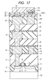
- FIG. 17 is a cross-sectional view showing a manufacturing method in Embodiment 1;
- FIG. 18 is a cross-sectional view showing a manufacturing method in Embodiment 1;
- FIG. 19 is a cross-sectional view showing a manufacturing method in Embodiment 1;
- FIG. 20 is a cross-sectional view showing a manufacturing method in Embodiment 1;
- FIG. 21 is a cross-sectional view showing a manufacturing method in Embodiment 1;
- FIG. 22 is a diagram showing experimental data of a semiconductor device according to Embodiment 1;
- FIG. 23 is a cross-sectional view showing the II-II cross-section of FIG. 1 in the case of Embodiment 2;
- FIG. 24 is a cross-sectional view showing a manufacturing method in Embodiment 2.
- FIG. 25 is a cross-sectional view showing a manufacturing method in Embodiment 2.
- FIG. 26 is a cross-sectional view showing a manufacturing method in Embodiment 2.
- a semiconductor device 90 according to this embodiment is a magnetic memory device (MRAM) using the MTJ element and provided with a plurality of bit lines 37 , a plurality of digit lines 25 d , a memory cell part MC including an MTJ element MD 1 , and a MOS transistor Q ( FIG. 2 ) controlling ON and OFF of a current flowing in the MTJ element MD 1 , as shown in FIG. 1 and FIG. 2 .
- MRAM magnetic memory device
- FIG. 2 MOS transistor Q
- the respective bit lines 37 are arranged in parallel over the horizontal plane having a spacing therebetween.
- the respective digit lines 25 d are arranged in parallel over the horizontal plane under the bit lines 37 having a spacing therebetween and also arranged so as to intersect the bit lines 37 perpendicularly.
- the memory cell part MC is provided with a bottom electrode EB 1 having a horizontally long rectangular shape in a planar view, a bottom magnetic film (Pin layer) 6 which is laminated on a part of the bottom electrode EB 1 upper surface on one end side and has a vertically long ellipsoidal shape in a planar view, a tunnel insulating film 7 laminated over the bottom magnetic film 6 , a top magnetic film (Free layer) 8 laminated over the tunnel insulating film 7 , a top electrode ET 1 laminated over the top magnetic film 8 , and a protection film 33 formed over the bottom electrode EB 1 so as to cover this laminated structure.
- the MTJ element MD 1 is composed of the bottom magnetic film 6 , the tunnel insulating film 7 , and the top magnetic film 8
- the MTJ element part is composed of the MTJ element MD 1 and the top electrode ET 1 .
- the amorphized metal nitride (e.g., TaN or WN) is used for the bottom electrode EB 1 .
- the thickness of the bottom electrode EB 1 is preferably 20 to 100 nm from the view point of a magnitude of resistance and peeling prevention of the protection film 33 . If the thickness is smaller than 20 nm, there is a possibility that the bottom electrode EB 1 becomes too thin by erosion in an etching process forming the bottom magnetic film 6 , and if the thickness is larger than 100 nm, there is a possibility that stress in the bottom electrode EB 1 becomes too high and the protection film 33 peels off.
- Pt, Ru, Mn, Co, Fe, a compound thereof, or the like, for example, is used for the bottom magnetic film 6 .
- Al-oxide, Mg-oxide, or the like, for example, is used for the tunnel insulating film 7 .
- Co, Fe, a compound thereof, or the like is used for the top magnetic film 8 .
- Ta, Ru, a laminated film thereof, or the like is used for the top electrode ET 1 .
- An insulating film containing nitrogen (nitride film, specifically silicon nitride, for example) is used for the protection film 33 .
- the thickness of the protection film 33 is preferably 50 to 100 nm from the viewpoint of oxidation prevention of the MTJ element MD 1 , the top electrode ET 1 , and the bottom electrode EB 1 .
- This memory cell part MC is disposed at the intersection of the digit line 25 d and the bit line 37 between both of the lines 25 d and 37 .
- the memory cell part MC is disposed such that the MTJ element MD 1 thereof is disposed at the intersection of both of the lines 25 d and 37 between both of the lines 25 d and 37 and also the bottom electrode EB 1 thereof is disposed along the bit line 37 .
- the upper surface of the top electrode ET 1 is coupled to the bit line 37 via an upper contact 37 a . Further, the lower surface of the bottom electrode EB 1 is coupled to a wiring 50 via a lower contact 30 . Note that the wiring 50 is connected to one of source and drain regions of the MOS transistor Q.
- the MOS transistor Q is formed over a semiconductor substrate 100 ( FIG. 2 ).
- An interlayer insulating film 60 is formed over the semiconductor substrate 100 so as to cover the MOS transistor Q, and the digit line 25 d , the memory cell part MC, and the wiring 50 are embedded in this interlayer insulating film 60 .
- the nitride film is used for the protection film 33 and the amorphized metal nitride is used for the bottom electrode EB 1 .
- Nitriding of a metal used for the bottom electrode EB 1 generates a coupling between nitrogen on the side of bottom electrode EB 1 and nitrogen on the side of protection film 33 and improves the adhesion between the bottom electrode EB 1 and the protection film 33 .
- amorphizing of a metal used for the bottom electrode EB 1 generates a dangling bond (uncoupled hand) over the surface of the bottom electrode EB 1 , and the protection film 33 is coupled with the dangling bond of the bottom electrode EB 1 when the protection film 33 is formed over the bottom electrode EB 1 , resulting in improvement of the adhesion between the bottom electrode EB 1 and the protection film 33 .
- the amorphizing of the bottom electrode EB 1 makes the surface of the bottom electrode EB 1 resistant to being damaged during the formation of the bottom electrode EB 1 , and also makes the bottom electrode EB 1 resistant to being expanded in volume by the heat treatment in the formation of the protection film 33 . Thereby, the protection film 33 becomes resistant to the peeling from the bottom electrode EB 1 .
- FIG. 3 to FIG. 21 are cross-sectional views showing a manufacturing method of the semiconductor device 90 of Embodiment 1. Note that each of FIG. 3 to FIG. 21 corresponds to the II-II cross-section of FIG. 1 .
- the manufacturing method of the semiconductor device of Embodiment 1 will be described with reference to FIG. 3 to FIG. 21 .
- an element isolation region is formed selectively in the upper layer of the semiconductor substrate 100 .
- the upper layer of the semiconductor substrate 100 between the element isolation regions 2 and 2 becomes an active region 1 where the transistor and the like are formed.
- a well region 1 w is formed in the upper layer of the semiconductor substrate 100 by introduction of an impurity of a first conductivity type.
- a gate insulating film 11 is formed over the well region 1 w , and a gate electrode 12 is formed selectively over the gate insulating film 11 .
- the surface of the well region 1 w under the gate electrode 12 is defined as a channel region 1 c.
- an impurity of a second conductivity type (opposite conductivity type to the first conductivity type) is implanted and diffused into the gate electrode 12 in a self alignment manner, and then a side wall 13 having a two-layer structure is formed on the lateral side of the gate electrode 12 .
- the impurity of second conductivity type is implanted and diffused into the gate electrode 12 and the side wall 13 in a self alignment manner to form a pair of source and drain regions 14 and 14 , which has an extension region near the channel region 1 c .
- the MOS transistor Q is formed which is composed of the channel region 1 c , the gate insulating film 11 , the gate electrode 12 , and the source and drain regions 14 .
- a cobalt silicide region 15 is formed over each surface of the source and drain regions 14 and 14 and the gate electrode 12 .
- an interlayer insulating film 16 is formed over the entire surface, and a contact plug 17 is formed selectively penetrating through the interlayer insulating film 16 .
- This contact plug 17 is electrically connected to one cobalt silicide region 15 of the pair of source and drain regions 14 and 14 .
- a nitride film 41 and an interlayer insulating film (oxide film) 18 are laminated over the entire surface, and a Cu wiring 19 is formed selectively penetrating through the nitride film 41 and the interlayer insulating film 18 . As a result, a part of the Cu wiring 19 is electrically connected to the contact plug 17 . In this manner, the Cu wiring 19 is formed as the first layer metal wiring.
- a nitride film 42 and interlayer insulating films (oxide films) 20 and 21 are laminated over the entire surface, and a fine hole 72 is formed selectively penetrating through the nitride film 42 and the interlayer insulating film 20 and further an interconnection hole 62 is formed selectively penetrating through the interlayer insulating film 21 over a region including the fine hole 72 .
- a Cu wiring 22 is formed filling the fine hole 72 and the interconnection hole 62 .
- the Cu wiring 22 is electrically connected to the Cu wiring 19 (Cu wiring 19 electrically connected to the contact plug 17 ). In this manner, the Cu wiring 22 is formed as the second layer metal wiring by use of a damascene technique.
- a nitride film 43 and interlayer insulating films (oxide films) 23 and 24 are formed over the entire surface and a fine hole 73 is formed selectively penetrating through the nitride film 43 and the interlayer insulating film 23 and further an interconnection hole 63 is formed selectively penetrating through the interlayer insulating film 24 over a region including the fine hole 73 .
- a Cu wiring 25 (lead line 25 r and digit line 25 d (word line)) is formed filling the fine hole 73 and the interconnection hole 63 .
- the lead line 25 r is electrically connected to the Cu wiring 22 . In this manner, the Cu wiring 25 is formed as the third layer metal wiring using the damascene technique.
- an interlayer insulating film 26 which is a silicon nitride film is formed over the entire surface, and a via hole 9 is formed penetrating through the interlayer insulating film 26 on a part of a region of the lead line 25 r.
- a barrier metal layer 28 is formed over the entire surface including the inside of the via hole 9 , and a via filling metal layer 29 is formed over the barrier metal layer 28 .
- the barrier metal layer 28 and the via filling metal layer 29 are subjected to CMP processing to leave only the barrier metal layer 28 within the via hole 9 and the via filling metal layer 29 .
- a bottom electrode layer 30 , a bottom magnetic layer 31 a , a tunnel insulating film 31 b , a top magnetic film 31 c and a top electrode layer 32 are laminated over the entire surface.
- the bottom magnetic layer 31 a , the tunnel insulating film 31 b , and the top magnetic film 31 c are called a MTJ film 31 .
- the amorphized metal nitride (e.g., Ta or WN) is used as the composition material of the bottom electrode EB 1
- Pt, Ru, Mn, Co, Fe, a compound thereof, or the like is used as the composition material of the bottom magnetic film 6
- Al-oxide, Mg-oxide, or the like for example, is used as the composition material of the tunnel insulating film 7
- Co, Fe, a compound thereof, or the like is used as the composition material of the top magnetic film 8
- Ta, Ru, a laminated film thereof, or the like is used as the composition material of the top electrode ET 1 .
- the bottom electrode EB 1 and the top electrode ET 1 are formed by a sputtering method, for example.
- the MTJ film 31 and the top electrode layer 32 are patterned by use of a patterned resist which is not shown in the drawing, and the MTJ element MD 1 and the top electrode ET 1 are obtained. These MTJ element MD 1 and top electrode ET 1 become the MTJ element part.
- a nitride film (e.g., silicon nitride film) is formed as the protection film 33 over the bottom. electrode 30 so as to cover the MTJ element part (MTJ element MD 1 and top electrode ET 1 ).
- the protection film 33 is formed at a temperature which does not affect the electro-magnetic characteristics of the magnetic material composing the MTJ element MD 1 (e.g., temperature of 300° C. or lower).
- the protection film 33 is formed strongly adhered to the bottom electrode 30 .
- the protection film 33 is also called a silicon nitride film 33 , hereinafter.
- a resist pattern 34 is formed selectively over the silicon nitride film 33 by use of a lithography technique.
- the silicon nitride film 33 and the bottom electrode layer 30 are patterned by use of a dry etching technique utilizing the resist pattern 34 as a mask, and the patterned silicon nitride film 33 and the bottom electrode EB 1 are obtained.
- the silicon nitride film 33 and the bottom electrode layer 30 are patterned at the same time in this manner, the surface and the lateral side of the MTJ element MD 1 are protected by the silicon nitride film 33 in the patterning of the bottom electrode layer 30 . Thereby, it is possible to effectively suppress leak current generation of the MTJ element MD 1 caused by a residual of the bottom electrode layer 30 attached to the lateral side of the MTJ element MD 1 or the like.
- FIG. 19 is an explanatory diagram showing an enlarged structure of the focused region v 1 of FIG. 18 .
- illustration of the silicon nitride film 33 is omitted from the drawing.
- the MTJ element part composed of the MTJ element MD 1 and the top electrode ET 1 can be obtained over the bottom electrode EB 1 .
- the detailed structure of the MTJ element MD 1 is the laminated structure of the bottom magnetic film 6 (Pin layer), the tunnel insulating film 7 , and the top magnetic film 8 (Free layer).
- an interlayer insulating film 35 made of SiO 2 is formed over the entire surface. In this process, even if hydrogen and water diffuse from the interlayer insulating film 35 , a magnetic damage thereof to the MTJ element MD 1 can be suppressed by the existence of the silicon nitride film 33 .
- the interlayer insulating film 35 is subjected to the CMP processing for planarization of the interlayer insulating film 35 .
- a via hole 40 is formed selectively over the top electrode ET 1 penetrating through the silicon nitride film 33 and the interlayer insulating film 35 .
- the silicon nitride film 33 functions as a stopper film for making the through hole in the interlayer insulating film 35 .
- a Cu wiring 37 a (upper contact) is embedded in the via hole 40 and also a Cu wiring 37 (bit line) is formed over the interlayer insulating film 35 .
- the Cu wiring 37 is electrically connected to the top electrode ET 1 of the MTJ element MD 1 through the via hole 40 .
- the Cu wiring 37 is formed as the fourth layer metal wiring.
- an interlayer insulating film (not shown in the drawing) is formed over the entire surface and the semiconductor device 9 , which is shown in FIG. 1 and FIG. 2 , is completed using the memory cell part MC composed of the bottom electrode EB 1 , the MTJ element MD 1 , the top electrode ET 1 , and the protection film 33 .
- the wiring 50 in FIG. 2 is composed of the respective parts 17 , 19 , 22 , and 25 r .
- the interlayer insulating film 60 in FIG. 2 is composed of the respective parts 16 , 18 , 20 , 21 , 23 , 24 , and 26 .
- the bottom electrode EB 1 is formed by the amorphized metal nitride (e.g., TaN or WN) by use of a reactive sputtering.
- the amorphized metal nitride e.g., TaN or WN
- An rf magnetron sputtering apparatus (base vacuum: 2 ⁇ 10 ⁇ 7 Torr and output: 150 W), for example, can be used as a film forming apparatus for the bottom electrode EB 1 .
- the bottom electrode EB 1 is formed by TaN, for example, Ta is used for a target and a gas mixture of Ar and N 2 , for example, is used for a sputter gas.
- the bottom electrode 30 made of the amorphized TaN is formed over the entire surface of the interlayer insulating film 26 so as to cover the respective parts 28 and 29 .
- the bottom electrode 30 is formed so as to have a thickness of 20 to 100 nm, for example.
- Ta atom is nitrided by increase of nitrogen to more than a certain amount in the sputtering atmosphere, and also nitrided Ta atom is amorphized and formed in a film state over the entire surface of the interlayer insulating film 26 .
- a metal other than Ta e.g., W
- the amorphized metal nitride is also formed by appropriate adjustment of the nitrogen ratio.
- the protection film 33 is formed by the nitride film (here, silicon nitride film).
- the silicon nitride film 33 is formed so as to satisfy first and second conditions to be described below.
- nitrogen is contained in a film forming gas for the silicon nitride film 33
- the magnetic film of the MTJ element MD 1 is nitrided by the nitrogen and the magnetization of the MTJ element MD 1 is deteriorated, and therefore a gas without containing NH 3 is used as the film forming gas (first condition).
- the silicon nitride film is formed at a film forming temperature not more than 200 to 350° C. for preventing the magnetization deterioration of the MTJ element MD 1 (second condition).
- a parallel plate type plasma CVD apparatus for example, can be used as a film forming apparatus for the silicon nitride film 33 .
- a film forming gas of SiH 4 /N 2 /helium (He) is used for satisfying the above first condition that NH 3 is not to be contained.
- the flow rate of SiH 4 , N 2 , and He can be set to be 1 to 500 sccm, 80 to 40,000 sccm, and 100 to 50,000 sccm, respectively.
- the film forming pressure, the electrode spacing between the parallel plates in the parallel plate type plasma CVD apparatus, and the RF power are set to be 1 to 20 Torr, 5 to 15 mm, and 0.1 to 10 W/cm 2 , respectively.
- the film forming temperature is set to be 200 to 350° C. for satisfying the above second condition.
- the upper limit temperature which does not affect the electro-magnetic characteristics of the magnetic material for the MTJ element MD 1 is 300° C. in the case that aluminum oxide (AlOx) such as alumina (Al 2 O 3 ) is used as the composition material of the tunnel insulating film 7 which composes the MTJ element MD 1 , and 350° C. in the case that magnesium oxide (MgO) is used as the composition material of the tunnel insulating film 7 .
- AlOx aluminum oxide
- Al 2 O 3 alumina
- MgO magnesium oxide
- the silicon nitride film 33 is formed in consideration of the above second condition, 200 to 300° C. is an ideal film forming temperature in the case that AlOx is used as the composition material of the tunnel insulating film 7 composing the MTJ element MD 1 , and 200 to 350° C. is an ideal film forming temperature in the case that MgO is used as the composition material of the tunnel insulating film 7 .
- the reason why the upper limit temperature is different between AlOx and MgO as the composition material of the tunnel insulating film 7 is as follows. AlOx is used in an amorphous state and MgO is used in a crystal state for the tunnel insulating film 7 (tunnel barrier). Therefore, MgO needs annealing for crystallization which requires an annealing temperature of about 350° C. However, too high annealing temperature deteriorates the magnetic characteristics of the Pin layer in the MTJ element MD 1 and the upper limit temperature is set to be 350° C. in consideration of this point. On the other hand, AlOx does not need the crystallization annealing since AlOx is used in the amorphous state. Accordingly, the upper limit temperature is set to be 300° C., since a low temperature process around 300° C. is required here.
- the reason why the lower limit of the film forming temperature is set to be 200° C. or higher is that it is practically difficult to form the silicon nitride film 33 at a film forming temperature lower than 200° C. using the parallel plate type plasma CVD apparatus.
- the silicon nitride film is formed as the protection film 33 under such a condition.
- FIG. 22 shows an experimental result verifying the improvement in the adhesion between the bottom electrode EB 1 and the protection film 33 in the semiconductor device 90 .
- Sample 1 is obtained in the following condition. That is, in the semiconductor device 90 , amorphized TaN is used as the composition material of the bottom electrode EB 1 , the bottom electrode EB 1 is polished by 5 nm by use of the CMP to have a final thickness of 35 nm, the silicon nitride film is used as the composition material of the protection film 33 , and a heat treatment temperature for forming the protection film 33 is 200° C.
- Sample 2 is obtained in the following condition. That is, in the semiconductor device 90 , amorphized TaN is used as the composition material of the bottom electrode EB 1 , the bottom electrode EB 1 is polished by 5 nm by use of the CMP to have a final thickness of 35 nm, the silicon nitride film is used as the composition material of the protection film 33 , and the heat treatment temperature for forming the protection film 33 is 275° C.
- Sample 3 is obtained in the following condition. That is, in the semiconductor device 90 , Ta is used as the composition material of the bottom electrode EB 1 , the bottom electrode EB 1 is polished by 20 nm by use of the CMP to have a final thickness of 50 nm, the silicon nitride film is used as the composition material of the protection film 33 , and the heat treatment temperature for forming the protection film 33 is 275° C.
- Sample 4 is obtained in the following condition. That is, in the semiconductor device 90 , Ta is used as the composition material of the bottom electrode EB 1 , the bottom electrode EB 1 is polished by 20 nm by use of the CMP to have a final thickness of 50 nm, the silicon nitride film is used as the composition material of the protection film 33 , and the heat treatment temperature for forming the protection film 33 is 200° C.
- Sample 5 is obtained in the following condition. That is, in the semiconductor device 90 , Ta is used as the composition material of the bottom electrode EB 1 , the stress in the bottom electrode EB 1 is made a low stress, the bottom electrode EB 1 is polished by 20 nm by use of the CMP to have a final thickness of 50 nm, the silicon nitride film is used as the composition material of the protection film 33 , and the heat treatment temperature for forming the protection film 33 is 275° C.
- the above low stress means a stress which is approximately one order smaller than stresses in the bottom electrodes EB 1 of Samples 1 to 4 and 7.
- the stresses in the bottom electrodes EB 1 of Samples 1 to 4 and 7 are several thousand MPa
- the stresses in the bottom electrodes EB 1 of Samples 5 and 6 are several hundred MPa.
- Sample 6 is obtained in the following condition. That is, in the semiconductor device 90 , Ta is used as the composition material of the bottom electrode EB 1 , the stress in the bottom electrode EB 1 is made the low stress, the bottom electrode EB 1 has a thickness of 30 nm without being polished, the silicon nitride film is used as the composition material of the protection film 33 , and the heat treatment temperature for forming the protection film 33 is 275° C.
- Sample 7 is obtained in the following condition. That is, in the semiconductor device 90 , amorphized TaN is used as the composition material of the bottom electrode EB 1 , the bottom electrode EB 1 has a thickness of 35 nm without being polished, the silicon nitride film is used as the composition material of the protection film 33 , and the heat treatment temperature for forming the protection film 33 is 275° C.
- the number of peeling positions in the protection film 33 is inspected by an optical inspection apparatus for one memory cell MC in each of Samples 1 to 7, and a result thereof indicates one position for Sample 1, zero positions for Samples 2, 3, and 7, ten positions for Sample 4, and ten or more positions for Samples 5 and 6.
- this experimental result particularly does not depend on a property inherent to Ta and apply also for a metal other than Ta. Accordingly, it turns out that the adhesion between the bottom electrode EB 1 and the protection film 33 is improved also by use of the amorphized metal nitride as the composition material of the bottom. electrode EB 1 . Further, since this experimental result also does not depend on a property inherent to Si, it turns out that the adhesion between the bottom electrode EB 1 and the protection film 33 is improved also by use of an insulating film containing nitrogen for the protection film 33 .
- the bottom electrode EB 1 is formed by the amorphized metal nitride (e.g., TaN or WN) and the protection film 33 is formed by the insulating film containing nitrogen (e.g., silicon nitride film), the adhesion is improved between the bottom electrode EB 1 and the protection film 33 .
- the protection film 33 is prevented from peeling off from the bottom electrode EB 1 and also it is possible to prevent the foreign material (H 2 , H 2 O, etc.) from intruding through the interface between the bottom electrode EB 1 and the protection film 33 , resulting in suppressing the deterioration in the characteristics of the MTJ element MD 1 .
- amorphized metal nitride is amorphized tantalum nitride (TaN), it is possible to improve the adhesion between the bottom electrode EB 1 and the protection film 33 by using a material easy to obtain.
- the above experimental data shows that the adhesion can be improved between the bottom electrode EB 1 and the protection film 33 also when the bottom electrode EB 1 is formed by tantalum nitride (TaN) and the protection film 33 is formed by the insulating film containing nitrogen (e.g., silicon nitride film).
- TaN tantalum nitride
- the protection film 33 is prevented from peeling off from the bottom electrode EB 1 and also the foreign material (H 2 , H 2 O, etc.) is prevented from intruding through the interface between the bottom electrode EB 1 and the protection film 33 , and thereby the deterioration of the characteristics of the MTJ element MD 1 can be suppressed.
- this embodiment includes the case that tantalum nitride (TaN) is used for the bottom electrode EB 1 .
- the bottom electrode EB 1 of Embodiment 1 is configured with a plurality (two in FIG. 23 ) of conductive layers 70 a and 70 b , and the top conductive layer 70 a is formed by the amorhousized metal nitride (e.g., TaN or WN) and the other conductive layer 70 b is formed by a metal which has a higher conductivity than the above amorphized metal nitride (i.e., low resistance metal) (e.g., Ta, W, Ti, and Cu).
- the different point from Embodiment 1 will be mainly described.
- the bottom electrode EB 1 is preferably formed to have a total thickness of 50 to 100 nm as in Embodiment 1 and the top layer conductive layer 70 a preferably has a thickness of 10 nm or larger. If the thickness is smaller than 10 nm, there is a possibility that the top conductive layer 70 a is eroded by etching during the formation of the bottom magnetic film 6 to expose the lower conductive layer 70 b.
- the bottom electrode EB 1 is configured with the two layers of the conductive layers 70 a and 70 b , and the upper (top) conductive layer 70 a is formed by the above amorphized metal nitride and the lower conductive layer 70 b is formed by the above metal which has a good conductivity.
- the MTJ element MD 1 and the top electrode ET 1 are laminated sequentially on a part of the upper conductive layer 70 a on one end side. Further, over the upper conductive layer 70 a , the protection film 33 is formed so as to cover the MTJ element MD 1 and the top electrode ET 1 . In this state, the protection film 33 is formed by the nitride film and also the upper conductive layer 70 a is formed by the amorphized metal nitride, and thereby the protection film 33 is formed to adhere strongly to the upper conductive layer 70 a.
- the manufacturing is carried out as same as in Embodiment 1.
- the lower conductive layer 70 b and the upper conductive layer 70 a are laminated sequentially over the entire surface of the interlayer insulating film 26 so as to cover the barrier metal layer 28 and the via filling metal layer 29 , and further thereon are sequentially laminated the bottom magnetic layer 31 a , the tunnel insulating film 31 b , the top magnetic film 31 c , and the top electrode layer 32 .
- the bottom magnetic layer 31 a , the tunnel insulating film 31 b , and the top magnetic film 31 c are called the MTJ film 31 .
- any one of Ta, W, Ti, and Cu is used as a composition material and a sputtering method, for example, is used for forming the lower conductive layer 70 b .
- a sputtering method for example, is used for forming the lower conductive layer 70 b .
- either TaN or WN, for example is used as the composition material and the reactive sputtering method is used as in Embodiment 1 for forming the upper conductive layer 70 b.
- the lower conductive layer 70 b and the upper conductive layer 70 a are formed, it is preferable to carry out film forming of the lower conductive layer 70 b and the upper conductive layer 70 a consecutively without taking out the semiconductor device 90 B under production from the chamber by using a sputtering apparatus which can selectively switch a plurality of targets (e.g., target for the lower conductive layer 70 b and target for the upper conductive layer 70 a ) in one chamber, for example.
- targets e.g., target for the lower conductive layer 70 b and target for the upper conductive layer 70 a
- the lower conductive layer 70 b and the upper conductive layer 70 a are consecutively by carrying the semiconductor device 90 B under production between the chambers without exposure to the air, using a sputtering apparatus which is provided with a plurality of chambers including a chamber for depositing the lower conductive layer 70 b and a chamber for film forming of the upper conductive layer 70 a .
- a sputtering apparatus which is provided with a plurality of chambers including a chamber for depositing the lower conductive layer 70 b and a chamber for film forming of the upper conductive layer 70 a .
- Such a film forming method can prevent the lower conductive layer 70 b from being exposed to the air.
- the MTJ film 31 and the top electrode layer 32 are patterned by use of a patterned resist which is not shown in the drawing, and the MTJ element MD 1 and the top electrode ET 1 are obtained. These MTJ element MD 1 and top electrode ET 1 become the MTJ element part.
- a nitride film (here, silicon nitride film) is formed over the upper conductive layer 70 a as the protection film 33 so as to cover the MTJ element part (MTJ element MD 1 and the top electrode ET 1 ), as in Embodiment 1.
- a patterned resist which is not shown in the drawing, the upper conductive layer 70 a , lower conductive layer 70 b , and the protection film 33 are patterned, and the bottom electrode EB 1 and the protection film 33 are obtained.
- the semiconductor device 90 B is completed after the upper contact 37 a and the bit line 37 are formed, as shown in FIG. 23 .
- the bottom electrode EB 1 is composed of the plurality of conductive layers (e.g., 70 a and 70 b ), and the top conductive layer 70 a among the plurality of conductive layers (conductive layer on which the conduction film is formed) is formed by the amorphized metal nitride (e.g., TaN or WN), the adhesion can be improved between the bottom electrode EB 1 and the protection film 33 .
- the amorphized metal nitride e.g., TaN or WN
- the other conductive layer 7 among the plurality of conductive layers is formed by the metal which has a higher conductivity than the amorphized metal nitride (i.e., low resistance metal) (e.g., Ta, W, Ti, or Cu), a good conductivity can be secured for the bottom electrode EB 1 .
- the metal which has a higher conductivity than the amorphized metal nitride i.e., low resistance metal
- this embodiment includes the case that tantalum nitride (TaN) is used for the bottom electrode EB 1 .
- TaN tantalum nitride
- the present invention can be applied to all the magnetic devices having the MTJ structure (particularly MRAM).
Landscapes
- Engineering & Computer Science (AREA)
- Computer Hardware Design (AREA)
- Manufacturing & Machinery (AREA)
- Mram Or Spin Memory Techniques (AREA)
- Hall/Mr Elements (AREA)
- Formation Of Insulating Films (AREA)
Abstract
To provide a semiconductor device that has an improved adhesion between a bottom conductive layer and a protection film protecting an MTJ element.
This semiconductor device includes a bottom electrode formed over a semiconductor substrate, an MTJ element part formed over a part of the bottom electrode by lamination of a bottom magnetic film, an insulating film, a top magnetic film, and a top electrode in this order, and a protection film formed over the bottom electrode so as to cover the MTJ element part, wherein the bottom electrode is formed by amorphized metal nitride and the protection film is formed by an insulating film containing nitrogen.
Description
This application is a Continuation of U.S. application Ser. No. 12/474,974, filed on May 29, 2009, claiming priority of Japanese Patent Application No. 2008-204442, filed on Aug. 7, 2008, the entire contents of each of which are hereby incorporated by reference.
This invention relates to a semiconductor device having a memory element such as an MTJ (Magnetic Tunnel Junction) element, and relates to a manufacturing method thereof.
An MRAM is a memory using a magnetic material for a memory element and storing data by a direction of magnetization of the magnetic material, that is, a memory retaining data by storing information in a spin of an electron, and has a circuit configured to be capable of random access. One of the memory element utilized for the MRAM is an MTJ element. Note that the present specification uses “MTJ element” as a concept including a TMR (Tunneling Magneto-Resistance) element.
A memory cell part of the MRAM is provided with a bottom electrode, a bottom magnetic film laminated over a part of the bottom electrode, a tunnel insulating film laminated over the bottom magnetic film, a top magnetic film laminated over the tunnel insulating film, a top electrode laminated over the top magnetic film, and a protection film formed over the bottom electrode so as to cover this laminated structure. Note that the MTJ element is composed of the above bottom magnetic film, tunnel insulating film, and top magnetic film.
Conventionally, Ta, Ti, or Cu, for example, has been used for the above bottom electrode and a nitride film or alumina, for example, has been used for the above protection film. As a prior art regarding such an MTJ element structure, Patent document 1 (Japanese patent laid-open No. 2007-158301) is known, for example.
Problem to be Solved by the Invention
In such an MTJ element, however, there is caused a failure that the protection film peels off from the bottom conductive layer when adhesion is low between the bottom conductive layer and the protection film, and there arises a problem that it is necessary to select a protection film of optimal material.
The peel-off of the protection film from the bottom electrode may be caused by the following reason. That is, the surface of the bottom electrode is damaged during formation of the bottom electrode, and, since the protection film is formed over the damaged surface, the protection film is likely to be peeled off. Then, the bottom electrode expands in volume due to heat treatment in the protection film formation and thereby the protection film peels off from the bottom electrode.
This invention has been made for solving the above problem and aims at providing a semiconductor device in which the adhesion is improved between the bottom electrode and the protection film protecting the MTJ element.
Means for Solving the Problem
According to a first aspect of this invention, a semiconductor device is provided with a bottom electrode formed over a semiconductor substrate, an MTJ element part formed over a part of the bottom electrode by lamination of a bottom magnetic film, an insulating film, a top magnetic film and a top electrode in this order, and a protection film formed over the bottom electrode so as to cover the MTJ element part, wherein the bottom electrode is formed by amorphized metal nitride and the protection film is formed by an insulating film containing nitrogen.
Advantage of the Invention
According to this first aspect, the bottom electrode is formed by the amorphized metal nitride and the protection film is formed by the insulating film containing nitrogen, and thereby the adhesion can be improved between the bottom electrode and the protection film. Accordingly, it is possible to prevent the protection film from peeling off from the bottom electrode and also to prevent foreign material (H2, H2O, etc.) from intruding through an interface between the bottom electrode and the protection film, and thereby suppressing deterioration of characteristics of the MTJ element.
<Configuration> A semiconductor device 90 according to this embodiment is a magnetic memory device (MRAM) using the MTJ element and provided with a plurality of bit lines 37, a plurality of digit lines 25 d, a memory cell part MC including an MTJ element MD1, and a MOS transistor Q (FIG. 2 ) controlling ON and OFF of a current flowing in the MTJ element MD1, as shown in FIG. 1 and FIG. 2 .
The respective bit lines 37 are arranged in parallel over the horizontal plane having a spacing therebetween. The respective digit lines 25 d are arranged in parallel over the horizontal plane under the bit lines 37 having a spacing therebetween and also arranged so as to intersect the bit lines 37 perpendicularly.
The memory cell part MC, as shown in FIG. 2 , is provided with a bottom electrode EB1 having a horizontally long rectangular shape in a planar view, a bottom magnetic film (Pin layer) 6 which is laminated on a part of the bottom electrode EB1 upper surface on one end side and has a vertically long ellipsoidal shape in a planar view, a tunnel insulating film 7 laminated over the bottom magnetic film 6, a top magnetic film (Free layer) 8 laminated over the tunnel insulating film 7, a top electrode ET1 laminated over the top magnetic film 8, and a protection film 33 formed over the bottom electrode EB1 so as to cover this laminated structure. Note that the MTJ element MD1 is composed of the bottom magnetic film 6, the tunnel insulating film 7, and the top magnetic film 8, and the MTJ element part is composed of the MTJ element MD1 and the top electrode ET1.
The amorphized metal nitride (e.g., TaN or WN) is used for the bottom electrode EB1. The thickness of the bottom electrode EB1 is preferably 20 to 100 nm from the view point of a magnitude of resistance and peeling prevention of the protection film 33. If the thickness is smaller than 20 nm, there is a possibility that the bottom electrode EB1 becomes too thin by erosion in an etching process forming the bottom magnetic film 6, and if the thickness is larger than 100 nm, there is a possibility that stress in the bottom electrode EB1 becomes too high and the protection film 33 peels off.
Pt, Ru, Mn, Co, Fe, a compound thereof, or the like, for example, is used for the bottom magnetic film 6. Al-oxide, Mg-oxide, or the like, for example, is used for the tunnel insulating film 7. Co, Fe, a compound thereof, or the like is used for the top magnetic film 8. Ta, Ru, a laminated film thereof, or the like is used for the top electrode ET1.
An insulating film containing nitrogen (nitride film, specifically silicon nitride, for example) is used for the protection film 33. The thickness of the protection film 33 is preferably 50 to 100 nm from the viewpoint of oxidation prevention of the MTJ element MD1, the top electrode ET1, and the bottom electrode EB1.
This memory cell part MC is disposed at the intersection of the digit line 25 d and the bit line 37 between both of the lines 25 d and 37. In more detail, the memory cell part MC is disposed such that the MTJ element MD1 thereof is disposed at the intersection of both of the lines 25 d and 37 between both of the lines 25 d and 37 and also the bottom electrode EB1 thereof is disposed along the bit line 37.
The upper surface of the top electrode ET1 is coupled to the bit line 37 via an upper contact 37 a. Further, the lower surface of the bottom electrode EB1 is coupled to a wiring 50 via a lower contact 30. Note that the wiring 50 is connected to one of source and drain regions of the MOS transistor Q.
The MOS transistor Q is formed over a semiconductor substrate 100 (FIG. 2 ). An interlayer insulating film 60 is formed over the semiconductor substrate 100 so as to cover the MOS transistor Q, and the digit line 25 d, the memory cell part MC, and the wiring 50 are embedded in this interlayer insulating film 60.
In this semiconductor device 90, the nitride film is used for the protection film 33 and the amorphized metal nitride is used for the bottom electrode EB1. Nitriding of a metal used for the bottom electrode EB1 generates a coupling between nitrogen on the side of bottom electrode EB1 and nitrogen on the side of protection film 33 and improves the adhesion between the bottom electrode EB1 and the protection film 33. Further, amorphizing of a metal used for the bottom electrode EB1 generates a dangling bond (uncoupled hand) over the surface of the bottom electrode EB1, and the protection film 33 is coupled with the dangling bond of the bottom electrode EB1 when the protection film 33 is formed over the bottom electrode EB1, resulting in improvement of the adhesion between the bottom electrode EB1 and the protection film 33.
Further, the amorphizing of the bottom electrode EB1 makes the surface of the bottom electrode EB1 resistant to being damaged during the formation of the bottom electrode EB1, and also makes the bottom electrode EB1 resistant to being expanded in volume by the heat treatment in the formation of the protection film 33. Thereby, the protection film 33 becomes resistant to the peeling from the bottom electrode EB1.
<Manufacturing method> FIG. 3 to FIG. 21 are cross-sectional views showing a manufacturing method of the semiconductor device 90 of Embodiment 1. Note that each of FIG. 3 to FIG. 21 corresponds to the II-II cross-section of FIG. 1 . Hereinbelow, the manufacturing method of the semiconductor device of Embodiment 1 will be described with reference to FIG. 3 to FIG. 21 .
First, as shown in FIG. 3 , an element isolation region is formed selectively in the upper layer of the semiconductor substrate 100. The upper layer of the semiconductor substrate 100 between the element isolation regions 2 and 2 becomes an active region 1 where the transistor and the like are formed.
Then, as shown in FIG. 4 , a well region 1 w is formed in the upper layer of the semiconductor substrate 100 by introduction of an impurity of a first conductivity type.
Next, as shown in FIG. 5 , a gate insulating film 11 is formed over the well region 1 w, and a gate electrode 12 is formed selectively over the gate insulating film 11. The surface of the well region 1 w under the gate electrode 12 is defined as a channel region 1 c.
Subsequently, as shown in FIG. 6 , an impurity of a second conductivity type (opposite conductivity type to the first conductivity type) is implanted and diffused into the gate electrode 12 in a self alignment manner, and then a side wall 13 having a two-layer structure is formed on the lateral side of the gate electrode 12. After that, the impurity of second conductivity type is implanted and diffused into the gate electrode 12 and the side wall 13 in a self alignment manner to form a pair of source and drain regions 14 and 14, which has an extension region near the channel region 1 c. As a result, the MOS transistor Q is formed which is composed of the channel region 1 c, the gate insulating film 11, the gate electrode 12, and the source and drain regions 14.
Next, as shown in FIG. 7 , a cobalt silicide region 15 is formed over each surface of the source and drain regions 14 and 14 and the gate electrode 12.
Subsequently, as shown in FIG. 8 , an interlayer insulating film 16 is formed over the entire surface, and a contact plug 17 is formed selectively penetrating through the interlayer insulating film 16. This contact plug 17 is electrically connected to one cobalt silicide region 15 of the pair of source and drain regions 14 and 14.
Further, as shown in FIG. 9 , a nitride film 41 and an interlayer insulating film (oxide film) 18 are laminated over the entire surface, and a Cu wiring 19 is formed selectively penetrating through the nitride film 41 and the interlayer insulating film 18. As a result, a part of the Cu wiring 19 is electrically connected to the contact plug 17. In this manner, the Cu wiring 19 is formed as the first layer metal wiring.
Subsequently, as shown in FIG. 10 , a nitride film 42 and interlayer insulating films (oxide films) 20 and 21 are laminated over the entire surface, and a fine hole 72 is formed selectively penetrating through the nitride film 42 and the interlayer insulating film 20 and further an interconnection hole 62 is formed selectively penetrating through the interlayer insulating film 21 over a region including the fine hole 72. After that, a Cu wiring 22 is formed filling the fine hole 72 and the interconnection hole 62. The Cu wiring 22 is electrically connected to the Cu wiring 19 (Cu wiring 19 electrically connected to the contact plug 17). In this manner, the Cu wiring 22 is formed as the second layer metal wiring by use of a damascene technique.
After that, as shown in FIG. 11 , a nitride film 43 and interlayer insulating films (oxide films) 23 and 24 are formed over the entire surface and a fine hole 73 is formed selectively penetrating through the nitride film 43 and the interlayer insulating film 23 and further an interconnection hole 63 is formed selectively penetrating through the interlayer insulating film 24 over a region including the fine hole 73. After that, a Cu wiring 25 (lead line 25 r and digit line 25 d (word line)) is formed filling the fine hole 73 and the interconnection hole 63. Then, the lead line 25 r is electrically connected to the Cu wiring 22. In this manner, the Cu wiring 25 is formed as the third layer metal wiring using the damascene technique.
After that, as shown in FIG. 12 , an interlayer insulating film 26 which is a silicon nitride film is formed over the entire surface, and a via hole 9 is formed penetrating through the interlayer insulating film 26 on a part of a region of the lead line 25 r.
Then, as shown in FIG. 13 , a barrier metal layer 28 is formed over the entire surface including the inside of the via hole 9, and a via filling metal layer 29 is formed over the barrier metal layer 28.
Subsequently, as shown in FIG. 14 , the barrier metal layer 28 and the via filling metal layer 29 are subjected to CMP processing to leave only the barrier metal layer 28 within the via hole 9 and the via filling metal layer 29.
After that, as shown FIG. 15 , a bottom electrode layer 30, a bottom magnetic layer 31 a, a tunnel insulating film 31 b, a top magnetic film 31 c and a top electrode layer 32 are laminated over the entire surface. Hereinafter, the bottom magnetic layer 31 a, the tunnel insulating film 31 b, and the top magnetic film 31 c are called a MTJ film 31.
In this process, the amorphized metal nitride (e.g., Ta or WN) is used as the composition material of the bottom electrode EB1, Pt, Ru, Mn, Co, Fe, a compound thereof, or the like, for example, is used as the composition material of the bottom magnetic film 6, Al-oxide, Mg-oxide, or the like, for example, is used as the composition material of the tunnel insulating film 7, Co, Fe, a compound thereof, or the like is used as the composition material of the top magnetic film 8, and Ta, Ru, a laminated film thereof, or the like is used as the composition material of the top electrode ET1. The bottom electrode EB1 and the top electrode ET1 are formed by a sputtering method, for example.
Subsequently, as shown in FIG. 16 , the MTJ film 31 and the top electrode layer 32 are patterned by use of a patterned resist which is not shown in the drawing, and the MTJ element MD1 and the top electrode ET1 are obtained. These MTJ element MD1 and top electrode ET1 become the MTJ element part.
Next, as shown in FIG. 17 , a nitride film (e.g., silicon nitride film) is formed as the protection film 33 over the bottom. electrode 30 so as to cover the MTJ element part (MTJ element MD1 and top electrode ET1). In this process, the protection film 33 is formed at a temperature which does not affect the electro-magnetic characteristics of the magnetic material composing the MTJ element MD1 (e.g., temperature of 300° C. or lower). In this condition, since the protection film 33 is formed by the nitride film and also the bottom electrode 30 is formed by the amorphized metal nitride, the protection film 33 is formed strongly adhered to the bottom electrode 30. Note that the protection film 33 is also called a silicon nitride film 33, hereinafter.
Then, a resist pattern 34 is formed selectively over the silicon nitride film 33 by use of a lithography technique.
Further, as shown in FIG. 18 , the silicon nitride film 33 and the bottom electrode layer 30 are patterned by use of a dry etching technique utilizing the resist pattern 34 as a mask, and the patterned silicon nitride film 33 and the bottom electrode EB1 are obtained.
Since the silicon nitride film 33 and the bottom electrode layer 30 are patterned at the same time in this manner, the surface and the lateral side of the MTJ element MD1 are protected by the silicon nitride film 33 in the patterning of the bottom electrode layer 30. Thereby, it is possible to effectively suppress leak current generation of the MTJ element MD1 caused by a residual of the bottom electrode layer 30 attached to the lateral side of the MTJ element MD1 or the like.
Next, as shown in FIG. 20 , an interlayer insulating film 35 made of SiO2 is formed over the entire surface. In this process, even if hydrogen and water diffuse from the interlayer insulating film 35, a magnetic damage thereof to the MTJ element MD1 can be suppressed by the existence of the silicon nitride film 33.
After that, as shown in FIG. 21 , the interlayer insulating film 35 is subjected to the CMP processing for planarization of the interlayer insulating film 35. Subsequently, a via hole 40 is formed selectively over the top electrode ET1 penetrating through the silicon nitride film 33 and the interlayer insulating film 35. At this time, the silicon nitride film 33 functions as a stopper film for making the through hole in the interlayer insulating film 35.
Next, a Cu wiring 37 a (upper contact) is embedded in the via hole 40 and also a Cu wiring 37 (bit line) is formed over the interlayer insulating film 35. As a result, the Cu wiring 37 is electrically connected to the top electrode ET1 of the MTJ element MD1 through the via hole 40. In this manner, the Cu wiring 37 is formed as the fourth layer metal wiring.
Lastly, an interlayer insulating film (not shown in the drawing) is formed over the entire surface and the semiconductor device 9, which is shown in FIG. 1 and FIG. 2 , is completed using the memory cell part MC composed of the bottom electrode EB1, the MTJ element MD1, the top electrode ET1, and the protection film 33. Note that the wiring 50 in FIG. 2 is composed of the respective parts 17, 19, 22, and 25 r. In addition, the interlayer insulating film 60 in FIG. 2 is composed of the respective parts 16, 18, 20, 21, 23, 24, and 26.
In the following, film forming methods will be described in detail for the bottom electrode EB1 and the protection film 33.
First a film forming method of the bottom electrode EB1 will be described in detail. The bottom electrode EB1 is formed by the amorphized metal nitride (e.g., TaN or WN) by use of a reactive sputtering.
An rf magnetron sputtering apparatus (base vacuum: 2×10⁻⁷ Torr and output: 150 W), for example, can be used as a film forming apparatus for the bottom electrode EB1. When the bottom electrode EB1 is formed by TaN, for example, Ta is used for a target and a gas mixture of Ar and N2, for example, is used for a sputter gas. At this time, a total flow amount of the gas mixture is 20 sccm, for example, and the flow rate of the gas mixture is Ar:N2=17:3, for example (nitrogen may be increased from this rate).
By the sputtering in this condition, as shown in FIG. 15 , the bottom electrode 30 made of the amorphized TaN is formed over the entire surface of the interlayer insulating film 26 so as to cover the respective parts 28 and 29. Here, the bottom electrode 30 is formed so as to have a thickness of 20 to 100 nm, for example.
That is, Ta atom is nitrided by increase of nitrogen to more than a certain amount in the sputtering atmosphere, and also nitrided Ta atom is amorphized and formed in a film state over the entire surface of the interlayer insulating film 26. When a metal other than Ta (e.g., W) is used, the amorphized metal nitride is also formed by appropriate adjustment of the nitrogen ratio.
Next, a film forming method of the protection film 33 will be described in detail. The protection film 33 is formed by the nitride film (here, silicon nitride film). In the following, the silicon nitride film 33 is formed so as to satisfy first and second conditions to be described below. When nitrogen is contained in a film forming gas for the silicon nitride film 33, the magnetic film of the MTJ element MD1 is nitrided by the nitrogen and the magnetization of the MTJ element MD1 is deteriorated, and therefore a gas without containing NH3 is used as the film forming gas (first condition). Further, the silicon nitride film is formed at a film forming temperature not more than 200 to 350° C. for preventing the magnetization deterioration of the MTJ element MD1 (second condition).
A parallel plate type plasma CVD apparatus, for example, can be used as a film forming apparatus for the silicon nitride film 33. A film forming gas of SiH4/N2/helium (He) is used for satisfying the above first condition that NH3 is not to be contained. For example, the flow rate of SiH4, N2, and He can be set to be 1 to 500 sccm, 80 to 40,000 sccm, and 100 to 50,000 sccm, respectively.
Further, the film forming pressure, the electrode spacing between the parallel plates in the parallel plate type plasma CVD apparatus, and the RF power are set to be 1 to 20 Torr, 5 to 15 mm, and 0.1 to 10 W/cm2, respectively. In addition, the film forming temperature is set to be 200 to 350° C. for satisfying the above second condition.
Note that the upper limit temperature which does not affect the electro-magnetic characteristics of the magnetic material for the MTJ element MD1 is 300° C. in the case that aluminum oxide (AlOx) such as alumina (Al2O3) is used as the composition material of the tunnel insulating film 7 which composes the MTJ element MD1, and 350° C. in the case that magnesium oxide (MgO) is used as the composition material of the tunnel insulating film 7.
Accordingly, when the silicon nitride film 33 is formed in consideration of the above second condition, 200 to 300° C. is an ideal film forming temperature in the case that AlOx is used as the composition material of the tunnel insulating film 7 composing the MTJ element MD1, and 200 to 350° C. is an ideal film forming temperature in the case that MgO is used as the composition material of the tunnel insulating film 7.
The reason why the upper limit temperature is different between AlOx and MgO as the composition material of the tunnel insulating film 7 is as follows. AlOx is used in an amorphous state and MgO is used in a crystal state for the tunnel insulating film 7 (tunnel barrier). Therefore, MgO needs annealing for crystallization which requires an annealing temperature of about 350° C. However, too high annealing temperature deteriorates the magnetic characteristics of the Pin layer in the MTJ element MD1 and the upper limit temperature is set to be 350° C. in consideration of this point. On the other hand, AlOx does not need the crystallization annealing since AlOx is used in the amorphous state. Accordingly, the upper limit temperature is set to be 300° C., since a low temperature process around 300° C. is required here.
Further, the reason why the lower limit of the film forming temperature is set to be 200° C. or higher is that it is practically difficult to form the silicon nitride film 33 at a film forming temperature lower than 200° C. using the parallel plate type plasma CVD apparatus. The silicon nitride film is formed as the protection film 33 under such a condition.
<Experimental data> FIG. 22 shows an experimental result verifying the improvement in the adhesion between the bottom electrode EB1 and the protection film 33 in the semiconductor device 90.
Sample 3 is obtained in the following condition. That is, in the semiconductor device 90, Ta is used as the composition material of the bottom electrode EB1, the bottom electrode EB1 is polished by 20 nm by use of the CMP to have a final thickness of 50 nm, the silicon nitride film is used as the composition material of the protection film 33, and the heat treatment temperature for forming the protection film 33 is 275° C.
Note that the above low stress means a stress which is approximately one order smaller than stresses in the bottom electrodes EB1 of Samples 1 to 4 and 7. Here, the stresses in the bottom electrodes EB1 of Samples 1 to 4 and 7 are several thousand MPa, and the stresses in the bottom electrodes EB1 of Samples 5 and 6 are several hundred MPa.
The number of peeling positions in the protection film 33 is inspected by an optical inspection apparatus for one memory cell MC in each of Samples 1 to 7, and a result thereof indicates one position for Sample 1, zero positions for Samples 2, 3, and 7, ten positions for Sample 4, and ten or more positions for Samples 5 and 6.
This result shows that the peeling of the protection film 33 is rarely detected for all Samples 1, 2, and 7 which use the nitrided Ta for the bottom electrode EB1. This is probably because a coupling is generated between nitrogen of TaN used for the bottom electrode EB1 and nitrogen of SiN used for the protection film 33 and improves the adhesion between the bottom electrode EB1 and the protection film 33.
Further, it is found that the peeling of the protection film 33 is rarely detected in all Samples 1, 2, and 7 which use amorphized Ta for the bottom electrodes EB1. This is probably because a dangling bond (uncoupled hand) is generated on the surface of the bottom electrode EB1 by the amorphousizing of Ta used for the bottom electrode EB1, and the protection film 33 is coupled with the dangling bond of the bottom electrode EB1 when the protection film 33 is formed over the bottom electrode EB1, to improve the adhesion between the bottom electrode EB1 and the protection film 33.
From this reason, it is presumed that this experimental result particularly does not depend on a property inherent to Ta and apply also for a metal other than Ta. Accordingly, it turns out that the adhesion between the bottom electrode EB1 and the protection film 33 is improved also by use of the amorphized metal nitride as the composition material of the bottom. electrode EB1. Further, since this experimental result also does not depend on a property inherent to Si, it turns out that the adhesion between the bottom electrode EB1 and the protection film 33 is improved also by use of an insulating film containing nitrogen for the protection film 33.
According to the above described semiconductor device and manufacturing method thereof, since the bottom electrode EB1 is formed by the amorphized metal nitride (e.g., TaN or WN) and the protection film 33 is formed by the insulating film containing nitrogen (e.g., silicon nitride film), the adhesion is improved between the bottom electrode EB1 and the protection film 33. Thereby, it is possible to prevent the protection film 33 from peeling off from the bottom electrode EB1 and also it is possible to prevent the foreign material (H2, H2O, etc.) from intruding through the interface between the bottom electrode EB1 and the protection film 33, resulting in suppressing the deterioration in the characteristics of the MTJ element MD1.
In addition, since the above amorphized metal nitride is amorphized tantalum nitride (TaN), it is possible to improve the adhesion between the bottom electrode EB1 and the protection film 33 by using a material easy to obtain.
Further, the above experimental data shows that the adhesion can be improved between the bottom electrode EB1 and the protection film 33 also when the bottom electrode EB1 is formed by tantalum nitride (TaN) and the protection film 33 is formed by the insulating film containing nitrogen (e.g., silicon nitride film). Thereby, it turns out that the protection film 33 is prevented from peeling off from the bottom electrode EB1 and also the foreign material (H2, H2O, etc.) is prevented from intruding through the interface between the bottom electrode EB1 and the protection film 33, and thereby the deterioration of the characteristics of the MTJ element MD1 can be suppressed. Accordingly, this embodiment includes the case that tantalum nitride (TaN) is used for the bottom electrode EB1.
In a semiconductor device 90B according to this embodiment, as shown in FIG. 23 , the bottom electrode EB1 of Embodiment 1 is configured with a plurality (two in FIG. 23 ) of conductive layers 70 a and 70 b, and the top conductive layer 70 a is formed by the amorhousized metal nitride (e.g., TaN or WN) and the other conductive layer 70 b is formed by a metal which has a higher conductivity than the above amorphized metal nitride (i.e., low resistance metal) (e.g., Ta, W, Ti, and Cu). In the following, the different point from Embodiment 1 will be mainly described.
In Embodiment 2, the bottom electrode EB1 is preferably formed to have a total thickness of 50 to 100 nm as in Embodiment 1 and the top layer conductive layer 70 a preferably has a thickness of 10 nm or larger. If the thickness is smaller than 10 nm, there is a possibility that the top conductive layer 70 a is eroded by etching during the formation of the bottom magnetic film 6 to expose the lower conductive layer 70 b.
In FIG. 23 , the bottom electrode EB1 is configured with the two layers of the conductive layers 70 a and 70 b, and the upper (top) conductive layer 70 a is formed by the above amorphized metal nitride and the lower conductive layer 70 b is formed by the above metal which has a good conductivity.
Then, the MTJ element MD1 and the top electrode ET1 are laminated sequentially on a part of the upper conductive layer 70 a on one end side. Further, over the upper conductive layer 70 a, the protection film 33 is formed so as to cover the MTJ element MD1 and the top electrode ET1. In this state, the protection film 33 is formed by the nitride film and also the upper conductive layer 70 a is formed by the amorphized metal nitride, and thereby the protection film 33 is formed to adhere strongly to the upper conductive layer 70 a.
Next, a manufacturing method of this semiconductor device 90B will be described according to FIG. 15 and FIG. 24 to FIG. 26 . In the following, only a different point from the manufacturing method in Embodiment 1 will be described.
Up to the process in FIG. 15 , the manufacturing is carried out as same as in Embodiment 1. Then, as shown in FIG. 24 , the lower conductive layer 70 b and the upper conductive layer 70 a are laminated sequentially over the entire surface of the interlayer insulating film 26 so as to cover the barrier metal layer 28 and the via filling metal layer 29, and further thereon are sequentially laminated the bottom magnetic layer 31 a, the tunnel insulating film 31 b, the top magnetic film 31 c, and the top electrode layer 32. In the following, the bottom magnetic layer 31 a, the tunnel insulating film 31 b, and the top magnetic film 31 c are called the MTJ film 31.
In the above process, any one of Ta, W, Ti, and Cu, for example, is used as a composition material and a sputtering method, for example, is used for forming the lower conductive layer 70 b. Further, either TaN or WN, for example, is used as the composition material and the reactive sputtering method is used as in Embodiment 1 for forming the upper conductive layer 70 b.
Note that, when the lower conductive layer 70 b and the upper conductive layer 70 a are formed, it is preferable to carry out film forming of the lower conductive layer 70 b and the upper conductive layer 70 a consecutively without taking out the semiconductor device 90B under production from the chamber by using a sputtering apparatus which can selectively switch a plurality of targets (e.g., target for the lower conductive layer 70 b and target for the upper conductive layer 70 a) in one chamber, for example. Alternatively, it is preferable to form the lower conductive layer 70 b and the upper conductive layer 70 a consecutively by carrying the semiconductor device 90B under production between the chambers without exposure to the air, using a sputtering apparatus which is provided with a plurality of chambers including a chamber for depositing the lower conductive layer 70 b and a chamber for film forming of the upper conductive layer 70 a. Such a film forming method can prevent the lower conductive layer 70 b from being exposed to the air.
Subsequently, as shown in FIG. 25 , the MTJ film 31 and the top electrode layer 32 are patterned by use of a patterned resist which is not shown in the drawing, and the MTJ element MD1 and the top electrode ET1 are obtained. These MTJ element MD1 and top electrode ET 1 become the MTJ element part.
Subsequently, as shown in FIG. 26 , a nitride film (here, silicon nitride film) is formed over the upper conductive layer 70 a as the protection film 33 so as to cover the MTJ element part (MTJ element MD1 and the top electrode ET1), as in Embodiment 1. Then, by use of a patterned resist which is not shown in the drawing, the upper conductive layer 70 a, lower conductive layer 70 b, and the protection film 33 are patterned, and the bottom electrode EB1 and the protection film 33 are obtained.
Then, as in Embodiment 1, the semiconductor device 90B is completed after the upper contact 37 a and the bit line 37 are formed, as shown in FIG. 23 .
According to the above described semiconductor device 90B and manufacturing method thereof, since the bottom electrode EB1 is composed of the plurality of conductive layers (e.g., 70 a and 70 b), and the top conductive layer 70 a among the plurality of conductive layers (conductive layer on which the conduction film is formed) is formed by the amorphized metal nitride (e.g., TaN or WN), the adhesion can be improved between the bottom electrode EB1 and the protection film 33. Further, since the other conductive layer 7 among the plurality of conductive layers is formed by the metal which has a higher conductivity than the amorphized metal nitride (i.e., low resistance metal) (e.g., Ta, W, Ti, or Cu), a good conductivity can be secured for the bottom electrode EB1.
Note that this embodiment includes the case that tantalum nitride (TaN) is used for the bottom electrode EB1.
Industrial Applicability
The present invention can be applied to all the magnetic devices having the MTJ structure (particularly MRAM).
Claims (6)
1. A semiconductor device, comprising:
a bottom electrode formed over a semiconductor substrate;
a Magnetic Tunnel Junction (MTJ) element formed over the bottom electrode by laminating a bottom magnetic film, an insulating film, a top magnetic film, and a top electrode in this order; and
a protection film formed over the bottom electrode so as to cover the MTJ element, the protection film partly making direct contact with the bottom electrode,
wherein the bottom electrode includes metal nitride, and
wherein the protection film includes nitrogen.
2. The semiconductor device according to claim 1 , wherein the metal nitride is amorphized metal nitride.
3. The semiconductor device according to claim 2 , wherein the amorphized metal nitride is amorphized tantalum nitride (TaN).
4. The semiconductor device according to claim 2 , wherein the amorphized metal nitride is amorphized tungsten nitride (WN).
5. The semiconductor device according to claim 1 , wherein the metal nitride is tungsten nitride (WN).
6. The semiconductor device according to claim 1 , wherein the protection film includes silicon nitride.
Priority Applications (1)
| Application Number | Priority Date | Filing Date | Title |
|---|---|---|---|
| US13/460,377 US8441083B2 (en) | 2008-08-07 | 2012-04-30 | Semiconductor device including a magnetic tunnel junction and method of manufacturing the same |
Applications Claiming Priority (4)
| Application Number | Priority Date | Filing Date | Title |
|---|---|---|---|
| JP2008204442A JP5203844B2 (en) | 2008-08-07 | 2008-08-07 | Semiconductor device and manufacturing method thereof |
| JP2008-204442 | 2008-08-07 | ||
| US12/474,974 US8264053B2 (en) | 2008-08-07 | 2009-05-29 | Semiconductor device including a magnetic tunnel junction and method of manufacturing the same |
| US13/460,377 US8441083B2 (en) | 2008-08-07 | 2012-04-30 | Semiconductor device including a magnetic tunnel junction and method of manufacturing the same |
Related Parent Applications (1)
| Application Number | Title | Priority Date | Filing Date |
|---|---|---|---|
| US12/474,974 Continuation US8264053B2 (en) | 2008-08-07 | 2009-05-29 | Semiconductor device including a magnetic tunnel junction and method of manufacturing the same |
Publications (2)
| Publication Number | Publication Date |
|---|---|
| US20120211847A1 US20120211847A1 (en) | 2012-08-23 |
| US8441083B2 true US8441083B2 (en) | 2013-05-14 |
Family
ID=41652117
Family Applications (2)
| Application Number | Title | Priority Date | Filing Date |
|---|---|---|---|
| US12/474,974 Expired - Fee Related US8264053B2 (en) | 2008-08-07 | 2009-05-29 | Semiconductor device including a magnetic tunnel junction and method of manufacturing the same |
| US13/460,377 Active US8441083B2 (en) | 2008-08-07 | 2012-04-30 | Semiconductor device including a magnetic tunnel junction and method of manufacturing the same |
Family Applications Before (1)
| Application Number | Title | Priority Date | Filing Date |
|---|---|---|---|
| US12/474,974 Expired - Fee Related US8264053B2 (en) | 2008-08-07 | 2009-05-29 | Semiconductor device including a magnetic tunnel junction and method of manufacturing the same |
Country Status (2)
| Country | Link |
|---|---|
| US (2) | US8264053B2 (en) |
| JP (1) | JP5203844B2 (en) |
Cited By (2)
| Publication number | Priority date | Publication date | Assignee | Title |
|---|---|---|---|---|
| US9647201B2 (en) | 2014-09-26 | 2017-05-09 | Samsung Electronics Co., Ltd. | Magnetic memory devices |
| US9893271B2 (en) | 2015-10-15 | 2018-02-13 | Samsung Electronics Co., Ltd. | Semiconductor memory device |
Families Citing this family (19)
| Publication number | Priority date | Publication date | Assignee | Title |
|---|---|---|---|---|
| US8557610B2 (en) * | 2011-02-14 | 2013-10-15 | Qualcomm Incorporated | Methods of integrated shielding into MTJ device for MRAM |
| JP2012182219A (en) | 2011-02-28 | 2012-09-20 | Toshiba Corp | Magnetic random access memory |
| JP2012204591A (en) * | 2011-03-25 | 2012-10-22 | Toshiba Corp | Film formation method and non-volatile storage device |
| US8866242B2 (en) | 2011-11-10 | 2014-10-21 | Qualcomm Incorporated | MTJ structure and integration scheme |
| CN103887422A (en) * | 2012-12-20 | 2014-06-25 | 中芯国际集成电路制造(上海)有限公司 | Magnetic random access memory and formation method thereof |
| CN104218150B (en) * | 2013-06-05 | 2017-03-22 | 中芯国际集成电路制造(上海)有限公司 | Forming method of magnetic random access memory unit |
| JP2015050339A (en) | 2013-09-02 | 2015-03-16 | ソニー株式会社 | Semiconductor device and manufacturing method of the same |
| US9231193B2 (en) | 2013-09-06 | 2016-01-05 | Masayoshi IWAYAMA | Magnetic memory and manufacturing method thereof |
| US9397289B2 (en) * | 2014-03-05 | 2016-07-19 | Kabushiki Kaisha Toshiba | Nonvolatile semiconductor memory device and method of manufacturing the same |
| US20150263267A1 (en) * | 2014-03-13 | 2015-09-17 | Hiroyuki Kanaya | Magnetic memory and method for manufacturing the same |
| KR102192205B1 (en) | 2014-04-28 | 2020-12-18 | 삼성전자주식회사 | Memory device |
| US9583535B2 (en) | 2015-05-01 | 2017-02-28 | Kabushiki Kaisha Toshiba | Magnetoresistive memory device and manufacturing method of the same |
| US9257136B1 (en) * | 2015-05-05 | 2016-02-09 | Micron Technology, Inc. | Magnetic tunnel junctions |
| US9780143B2 (en) * | 2015-08-25 | 2017-10-03 | Western Digital Technologies, Inc. | Implementing magnetic memory integration with CMOS driving circuits |
| US9680089B1 (en) | 2016-05-13 | 2017-06-13 | Micron Technology, Inc. | Magnetic tunnel junctions |
| US10347825B2 (en) | 2017-02-17 | 2019-07-09 | International Business Machines Corporation | Selective deposition and nitridization of bottom electrode metal for MRAM applications |
| US10741748B2 (en) | 2018-06-25 | 2020-08-11 | International Business Machines Corporation | Back end of line metallization structures |
| US10903417B2 (en) * | 2019-02-04 | 2021-01-26 | International Business Machines Corporation | MTJ containing device with replacement top electrode |
| JP7441483B2 (en) * | 2019-08-23 | 2024-03-01 | 国立大学法人東北大学 | Magnetic memory element and its manufacturing method, and magnetic memory |
Citations (7)
| Publication number | Priority date | Publication date | Assignee | Title |
|---|---|---|---|---|
| US6358756B1 (en) * | 2001-02-07 | 2002-03-19 | Micron Technology, Inc. | Self-aligned, magnetoresistive random-access memory (MRAM) structure utilizing a spacer containment scheme |
| JP2003243630A (en) | 2002-02-18 | 2003-08-29 | Sony Corp | Magnetic memory device and method of manufacturing the same |
| JP2004319725A (en) | 2003-04-16 | 2004-11-11 | Fujitsu Ltd | Magnetic random access memory device |
| JP2006019743A (en) | 2004-06-30 | 2006-01-19 | Headway Technologies Inc | Magnetic memory structure, tunnel magneto-resistance effect type reproducing head, and their manufacturing method |
| WO2006070803A1 (en) | 2004-12-28 | 2006-07-06 | Nec Corporation | Magnetic random access memory and method for manufacturing same |
| US20060220083A1 (en) * | 2005-01-26 | 2006-10-05 | Oki Electric Industry Co., Ltd. | Semiconductor device |
| US20070108543A1 (en) | 2005-11-14 | 2007-05-17 | Haruo Furuta | Semiconductor device and method of manufacturing the same |
Family Cites Families (1)
| Publication number | Priority date | Publication date | Assignee | Title |
|---|---|---|---|---|
| JP4190259B2 (en) * | 2002-11-11 | 2008-12-03 | シャープ株式会社 | Active matrix substrate, manufacturing method thereof, and display device |
-
2008
- 2008-08-07 JP JP2008204442A patent/JP5203844B2/en not_active Expired - Fee Related
-
2009
- 2009-05-29 US US12/474,974 patent/US8264053B2/en not_active Expired - Fee Related
-
2012
- 2012-04-30 US US13/460,377 patent/US8441083B2/en active Active
Patent Citations (10)
| Publication number | Priority date | Publication date | Assignee | Title |
|---|---|---|---|---|
| US6358756B1 (en) * | 2001-02-07 | 2002-03-19 | Micron Technology, Inc. | Self-aligned, magnetoresistive random-access memory (MRAM) structure utilizing a spacer containment scheme |
| JP2003243630A (en) | 2002-02-18 | 2003-08-29 | Sony Corp | Magnetic memory device and method of manufacturing the same |
| US6998665B2 (en) | 2002-02-18 | 2006-02-14 | Sony Corporation | Magnetic memory device and manufacturing method therefor |
| JP2004319725A (en) | 2003-04-16 | 2004-11-11 | Fujitsu Ltd | Magnetic random access memory device |
| JP2006019743A (en) | 2004-06-30 | 2006-01-19 | Headway Technologies Inc | Magnetic memory structure, tunnel magneto-resistance effect type reproducing head, and their manufacturing method |
| US7611912B2 (en) | 2004-06-30 | 2009-11-03 | Headway Technologies, Inc. | Underlayer for high performance magnetic tunneling junction MRAM |
| WO2006070803A1 (en) | 2004-12-28 | 2006-07-06 | Nec Corporation | Magnetic random access memory and method for manufacturing same |
| US20060220083A1 (en) * | 2005-01-26 | 2006-10-05 | Oki Electric Industry Co., Ltd. | Semiconductor device |
| US20070108543A1 (en) | 2005-11-14 | 2007-05-17 | Haruo Furuta | Semiconductor device and method of manufacturing the same |
| JP2007158301A (en) | 2005-11-14 | 2007-06-21 | Renesas Technology Corp | Semiconductor device and manufacturing method thereof |
Non-Patent Citations (2)
| Title |
|---|
| Japanese Notice of Reasons for Refusal, and English translation thereof, issued in Japanese Patent Application No. 2008-204442, dated Nov. 6, 2012. |
| Japanese Office Action with English Translation issued in Japanese Application No. 2008-204442 issued on Apr. 3, 2012. |
Cited By (2)
| Publication number | Priority date | Publication date | Assignee | Title |
|---|---|---|---|---|
| US9647201B2 (en) | 2014-09-26 | 2017-05-09 | Samsung Electronics Co., Ltd. | Magnetic memory devices |
| US9893271B2 (en) | 2015-10-15 | 2018-02-13 | Samsung Electronics Co., Ltd. | Semiconductor memory device |
Also Published As
| Publication number | Publication date |
|---|---|
| US20120211847A1 (en) | 2012-08-23 |
| US20100032779A1 (en) | 2010-02-11 |
| JP5203844B2 (en) | 2013-06-05 |
| US8264053B2 (en) | 2012-09-11 |
| JP2010040928A (en) | 2010-02-18 |
Similar Documents
| Publication | Publication Date | Title |
|---|---|---|
| US8441083B2 (en) | Semiconductor device including a magnetic tunnel junction and method of manufacturing the same | |
| US11005032B2 (en) | Techniques for MRAM MTJ top electrode to metal layer interface including spacer | |
| US7772662B2 (en) | Semiconductor device and manufacturing method thereof | |
| US8216859B2 (en) | Manufacturing method of semiconductor device having memory element with protective film | |
| US20200082860A1 (en) | Magnetic random access memory structure and manufacturing method of the same | |
| US8258592B2 (en) | Semiconductor device including a magnetic tunnel junction device including a laminated structure and manufacturing method therefor | |
| US11839161B2 (en) | Semiconductor structure | |
| US8772845B2 (en) | Technique for smoothing an interface between layers of a semiconductor device | |
| US9716222B1 (en) | Semiconductor structure and method for manufacturing the same | |
| US11665970B2 (en) | Magnetoresistive random access memory (MRAM) device | |
| US20100264501A1 (en) | Method for manufacturing magnetic storage device and magnetic storage device | |
| US10957847B2 (en) | Multilayered spacer structure for a magnetic tunneling junction and method of manufacturing | |
| US9015927B2 (en) | Method for fabricating synthetic antiferromagnetic (SAF) device | |
| US11056643B2 (en) | Magnetic tunnel junction (MTJ) hard mask encapsulation to prevent redeposition | |
| US20240016062A1 (en) | Method of fabricating magnetic tunneling junction device | |
| JP2012142415A (en) | Magnetic device and method of manufacturing the same |
Legal Events
| Date | Code | Title | Description |
|---|---|---|---|
| STCF | Information on status: patent grant |
Free format text: PATENTED CASE |
|
| FPAY | Fee payment |
Year of fee payment: 4 |
|
| AS | Assignment |
Owner name: RENESAS ELECTRONICS CORPORATION, JAPAN Free format text: CHANGE OF ADDRESS;ASSIGNOR:RENESAS ELECTRONICS CORPORATION;REEL/FRAME:044928/0001 Effective date: 20150806 |
|
| MAFP | Maintenance fee payment |
Free format text: PAYMENT OF MAINTENANCE FEE, 8TH YEAR, LARGE ENTITY (ORIGINAL EVENT CODE: M1552); ENTITY STATUS OF PATENT OWNER: LARGE ENTITY Year of fee payment: 8 |