US8508041B2 - Bonding method for three-dimensional integrated circuit and three-dimensional integrated circuit thereof - Google Patents
Bonding method for three-dimensional integrated circuit and three-dimensional integrated circuit thereof Download PDFInfo
- Publication number
- US8508041B2 US8508041B2 US13/325,587 US201113325587A US8508041B2 US 8508041 B2 US8508041 B2 US 8508041B2 US 201113325587 A US201113325587 A US 201113325587A US 8508041 B2 US8508041 B2 US 8508041B2
- Authority
- US
- United States
- Prior art keywords
- metal
- integrated circuit
- layer
- deposition layer
- dimensional integrated
- Prior art date
- Legal status (The legal status is an assumption and is not a legal conclusion. Google has not performed a legal analysis and makes no representation as to the accuracy of the status listed.)
- Active - Reinstated, expires
Links
Images


Classifications
-
- H—ELECTRICITY
- H01—ELECTRIC ELEMENTS
- H01L—SEMICONDUCTOR DEVICES NOT COVERED BY CLASS H10
- H01L21/00—Processes or apparatus adapted for the manufacture or treatment of semiconductor or solid state devices or of parts thereof
- H01L21/02—Manufacture or treatment of semiconductor devices or of parts thereof
- H01L21/04—Manufacture or treatment of semiconductor devices or of parts thereof the devices having at least one potential-jump barrier or surface barrier, e.g. PN junction, depletion layer or carrier concentration layer
- H01L21/18—Manufacture or treatment of semiconductor devices or of parts thereof the devices having at least one potential-jump barrier or surface barrier, e.g. PN junction, depletion layer or carrier concentration layer the devices having semiconductor bodies comprising elements of Group IV of the Periodic System or AIIIBV compounds with or without impurities, e.g. doping materials
- H01L21/20—Deposition of semiconductor materials on a substrate, e.g. epitaxial growth solid phase epitaxy
-
- H—ELECTRICITY
- H01—ELECTRIC ELEMENTS
- H01L—SEMICONDUCTOR DEVICES NOT COVERED BY CLASS H10
- H01L24/00—Arrangements for connecting or disconnecting semiconductor or solid-state bodies; Methods or apparatus related thereto
- H01L24/01—Means for bonding being attached to, or being formed on, the surface to be connected, e.g. chip-to-package, die-attach, "first-level" interconnects; Manufacturing methods related thereto
- H01L24/10—Bump connectors ; Manufacturing methods related thereto
- H01L24/11—Manufacturing methods
-
- H—ELECTRICITY
- H01—ELECTRIC ELEMENTS
- H01L—SEMICONDUCTOR DEVICES NOT COVERED BY CLASS H10
- H01L24/00—Arrangements for connecting or disconnecting semiconductor or solid-state bodies; Methods or apparatus related thereto
- H01L24/01—Means for bonding being attached to, or being formed on, the surface to be connected, e.g. chip-to-package, die-attach, "first-level" interconnects; Manufacturing methods related thereto
- H01L24/10—Bump connectors ; Manufacturing methods related thereto
- H01L24/12—Structure, shape, material or disposition of the bump connectors prior to the connecting process
- H01L24/13—Structure, shape, material or disposition of the bump connectors prior to the connecting process of an individual bump connector
-
- H—ELECTRICITY
- H01—ELECTRIC ELEMENTS
- H01L—SEMICONDUCTOR DEVICES NOT COVERED BY CLASS H10
- H01L24/00—Arrangements for connecting or disconnecting semiconductor or solid-state bodies; Methods or apparatus related thereto
- H01L24/01—Means for bonding being attached to, or being formed on, the surface to be connected, e.g. chip-to-package, die-attach, "first-level" interconnects; Manufacturing methods related thereto
- H01L24/10—Bump connectors ; Manufacturing methods related thereto
- H01L24/15—Structure, shape, material or disposition of the bump connectors after the connecting process
- H01L24/16—Structure, shape, material or disposition of the bump connectors after the connecting process of an individual bump connector
-
- H—ELECTRICITY
- H01—ELECTRIC ELEMENTS
- H01L—SEMICONDUCTOR DEVICES NOT COVERED BY CLASS H10
- H01L24/00—Arrangements for connecting or disconnecting semiconductor or solid-state bodies; Methods or apparatus related thereto
- H01L24/80—Methods for connecting semiconductor or other solid state bodies using means for bonding being attached to, or being formed on, the surface to be connected
- H01L24/81—Methods for connecting semiconductor or other solid state bodies using means for bonding being attached to, or being formed on, the surface to be connected using a bump connector
-
- H—ELECTRICITY
- H01—ELECTRIC ELEMENTS
- H01L—SEMICONDUCTOR DEVICES NOT COVERED BY CLASS H10
- H01L25/00—Assemblies consisting of a plurality of individual semiconductor or other solid state devices ; Multistep manufacturing processes thereof
- H01L25/03—Assemblies consisting of a plurality of individual semiconductor or other solid state devices ; Multistep manufacturing processes thereof all the devices being of a type provided for in the same subgroup of groups H01L27/00 - H01L33/00, or in a single subclass of H10K, H10N, e.g. assemblies of rectifier diodes
- H01L25/04—Assemblies consisting of a plurality of individual semiconductor or other solid state devices ; Multistep manufacturing processes thereof all the devices being of a type provided for in the same subgroup of groups H01L27/00 - H01L33/00, or in a single subclass of H10K, H10N, e.g. assemblies of rectifier diodes the devices not having separate containers
- H01L25/065—Assemblies consisting of a plurality of individual semiconductor or other solid state devices ; Multistep manufacturing processes thereof all the devices being of a type provided for in the same subgroup of groups H01L27/00 - H01L33/00, or in a single subclass of H10K, H10N, e.g. assemblies of rectifier diodes the devices not having separate containers the devices being of a type provided for in group H01L27/00
- H01L25/0657—Stacked arrangements of devices
-
- H—ELECTRICITY
- H01—ELECTRIC ELEMENTS
- H01L—SEMICONDUCTOR DEVICES NOT COVERED BY CLASS H10
- H01L25/00—Assemblies consisting of a plurality of individual semiconductor or other solid state devices ; Multistep manufacturing processes thereof
- H01L25/50—Multistep manufacturing processes of assemblies consisting of devices, each device being of a type provided for in group H01L27/00 or H01L29/00
-
- H—ELECTRICITY
- H01—ELECTRIC ELEMENTS
- H01L—SEMICONDUCTOR DEVICES NOT COVERED BY CLASS H10
- H01L2224/00—Indexing scheme for arrangements for connecting or disconnecting semiconductor or solid-state bodies and methods related thereto as covered by H01L24/00
- H01L2224/01—Means for bonding being attached to, or being formed on, the surface to be connected, e.g. chip-to-package, die-attach, "first-level" interconnects; Manufacturing methods related thereto
- H01L2224/10—Bump connectors; Manufacturing methods related thereto
- H01L2224/11—Manufacturing methods
- H01L2224/114—Manufacturing methods by blanket deposition of the material of the bump connector
- H01L2224/11444—Manufacturing methods by blanket deposition of the material of the bump connector in gaseous form
- H01L2224/1145—Physical vapour deposition [PVD], e.g. evaporation, or sputtering
-
- H—ELECTRICITY
- H01—ELECTRIC ELEMENTS
- H01L—SEMICONDUCTOR DEVICES NOT COVERED BY CLASS H10
- H01L2224/00—Indexing scheme for arrangements for connecting or disconnecting semiconductor or solid-state bodies and methods related thereto as covered by H01L24/00
- H01L2224/01—Means for bonding being attached to, or being formed on, the surface to be connected, e.g. chip-to-package, die-attach, "first-level" interconnects; Manufacturing methods related thereto
- H01L2224/10—Bump connectors; Manufacturing methods related thereto
- H01L2224/12—Structure, shape, material or disposition of the bump connectors prior to the connecting process
- H01L2224/13—Structure, shape, material or disposition of the bump connectors prior to the connecting process of an individual bump connector
- H01L2224/13001—Core members of the bump connector
- H01L2224/13075—Plural core members
- H01L2224/1308—Plural core members being stacked
- H01L2224/13082—Two-layer arrangements
-
- H—ELECTRICITY
- H01—ELECTRIC ELEMENTS
- H01L—SEMICONDUCTOR DEVICES NOT COVERED BY CLASS H10
- H01L2224/00—Indexing scheme for arrangements for connecting or disconnecting semiconductor or solid-state bodies and methods related thereto as covered by H01L24/00
- H01L2224/01—Means for bonding being attached to, or being formed on, the surface to be connected, e.g. chip-to-package, die-attach, "first-level" interconnects; Manufacturing methods related thereto
- H01L2224/10—Bump connectors; Manufacturing methods related thereto
- H01L2224/12—Structure, shape, material or disposition of the bump connectors prior to the connecting process
- H01L2224/13—Structure, shape, material or disposition of the bump connectors prior to the connecting process of an individual bump connector
- H01L2224/13001—Core members of the bump connector
- H01L2224/13099—Material
- H01L2224/131—Material with a principal constituent of the material being a metal or a metalloid, e.g. boron [B], silicon [Si], germanium [Ge], arsenic [As], antimony [Sb], tellurium [Te] and polonium [Po], and alloys thereof
- H01L2224/13138—Material with a principal constituent of the material being a metal or a metalloid, e.g. boron [B], silicon [Si], germanium [Ge], arsenic [As], antimony [Sb], tellurium [Te] and polonium [Po], and alloys thereof the principal constituent melting at a temperature of greater than or equal to 950°C and less than 1550°C
- H01L2224/13147—Copper [Cu] as principal constituent
-
- H—ELECTRICITY
- H01—ELECTRIC ELEMENTS
- H01L—SEMICONDUCTOR DEVICES NOT COVERED BY CLASS H10
- H01L2224/00—Indexing scheme for arrangements for connecting or disconnecting semiconductor or solid-state bodies and methods related thereto as covered by H01L24/00
- H01L2224/01—Means for bonding being attached to, or being formed on, the surface to be connected, e.g. chip-to-package, die-attach, "first-level" interconnects; Manufacturing methods related thereto
- H01L2224/10—Bump connectors; Manufacturing methods related thereto
- H01L2224/12—Structure, shape, material or disposition of the bump connectors prior to the connecting process
- H01L2224/13—Structure, shape, material or disposition of the bump connectors prior to the connecting process of an individual bump connector
- H01L2224/13001—Core members of the bump connector
- H01L2224/13099—Material
- H01L2224/131—Material with a principal constituent of the material being a metal or a metalloid, e.g. boron [B], silicon [Si], germanium [Ge], arsenic [As], antimony [Sb], tellurium [Te] and polonium [Po], and alloys thereof
- H01L2224/13163—Material with a principal constituent of the material being a metal or a metalloid, e.g. boron [B], silicon [Si], germanium [Ge], arsenic [As], antimony [Sb], tellurium [Te] and polonium [Po], and alloys thereof the principal constituent melting at a temperature of greater than 1550°C
- H01L2224/13166—Titanium [Ti] as principal constituent
-
- H—ELECTRICITY
- H01—ELECTRIC ELEMENTS
- H01L—SEMICONDUCTOR DEVICES NOT COVERED BY CLASS H10
- H01L2224/00—Indexing scheme for arrangements for connecting or disconnecting semiconductor or solid-state bodies and methods related thereto as covered by H01L24/00
- H01L2224/01—Means for bonding being attached to, or being formed on, the surface to be connected, e.g. chip-to-package, die-attach, "first-level" interconnects; Manufacturing methods related thereto
- H01L2224/10—Bump connectors; Manufacturing methods related thereto
- H01L2224/15—Structure, shape, material or disposition of the bump connectors after the connecting process
- H01L2224/16—Structure, shape, material or disposition of the bump connectors after the connecting process of an individual bump connector
- H01L2224/161—Disposition
- H01L2224/16135—Disposition the bump connector connecting between different semiconductor or solid-state bodies, i.e. chip-to-chip
- H01L2224/16137—Disposition the bump connector connecting between different semiconductor or solid-state bodies, i.e. chip-to-chip the bodies being arranged next to each other, e.g. on a common substrate
-
- H—ELECTRICITY
- H01—ELECTRIC ELEMENTS
- H01L—SEMICONDUCTOR DEVICES NOT COVERED BY CLASS H10
- H01L2224/00—Indexing scheme for arrangements for connecting or disconnecting semiconductor or solid-state bodies and methods related thereto as covered by H01L24/00
- H01L2224/01—Means for bonding being attached to, or being formed on, the surface to be connected, e.g. chip-to-package, die-attach, "first-level" interconnects; Manufacturing methods related thereto
- H01L2224/10—Bump connectors; Manufacturing methods related thereto
- H01L2224/15—Structure, shape, material or disposition of the bump connectors after the connecting process
- H01L2224/16—Structure, shape, material or disposition of the bump connectors after the connecting process of an individual bump connector
- H01L2224/161—Disposition
- H01L2224/16135—Disposition the bump connector connecting between different semiconductor or solid-state bodies, i.e. chip-to-chip
- H01L2224/16145—Disposition the bump connector connecting between different semiconductor or solid-state bodies, i.e. chip-to-chip the bodies being stacked
-
- H—ELECTRICITY
- H01—ELECTRIC ELEMENTS
- H01L—SEMICONDUCTOR DEVICES NOT COVERED BY CLASS H10
- H01L2224/00—Indexing scheme for arrangements for connecting or disconnecting semiconductor or solid-state bodies and methods related thereto as covered by H01L24/00
- H01L2224/01—Means for bonding being attached to, or being formed on, the surface to be connected, e.g. chip-to-package, die-attach, "first-level" interconnects; Manufacturing methods related thereto
- H01L2224/10—Bump connectors; Manufacturing methods related thereto
- H01L2224/15—Structure, shape, material or disposition of the bump connectors after the connecting process
- H01L2224/16—Structure, shape, material or disposition of the bump connectors after the connecting process of an individual bump connector
- H01L2224/165—Material
- H01L2224/16501—Material at the bonding interface
-
- H—ELECTRICITY
- H01—ELECTRIC ELEMENTS
- H01L—SEMICONDUCTOR DEVICES NOT COVERED BY CLASS H10
- H01L2224/00—Indexing scheme for arrangements for connecting or disconnecting semiconductor or solid-state bodies and methods related thereto as covered by H01L24/00
- H01L2224/01—Means for bonding being attached to, or being formed on, the surface to be connected, e.g. chip-to-package, die-attach, "first-level" interconnects; Manufacturing methods related thereto
- H01L2224/10—Bump connectors; Manufacturing methods related thereto
- H01L2224/15—Structure, shape, material or disposition of the bump connectors after the connecting process
- H01L2224/16—Structure, shape, material or disposition of the bump connectors after the connecting process of an individual bump connector
- H01L2224/165—Material
- H01L2224/16505—Material outside the bonding interface, e.g. in the bulk of the bump connector
-
- H—ELECTRICITY
- H01—ELECTRIC ELEMENTS
- H01L—SEMICONDUCTOR DEVICES NOT COVERED BY CLASS H10
- H01L2224/00—Indexing scheme for arrangements for connecting or disconnecting semiconductor or solid-state bodies and methods related thereto as covered by H01L24/00
- H01L2224/80—Methods for connecting semiconductor or other solid state bodies using means for bonding being attached to, or being formed on, the surface to be connected
- H01L2224/81—Methods for connecting semiconductor or other solid state bodies using means for bonding being attached to, or being formed on, the surface to be connected using a bump connector
- H01L2224/81053—Bonding environment
- H01L2224/81054—Composition of the atmosphere
- H01L2224/81055—Composition of the atmosphere being oxidating
-
- H—ELECTRICITY
- H01—ELECTRIC ELEMENTS
- H01L—SEMICONDUCTOR DEVICES NOT COVERED BY CLASS H10
- H01L2224/00—Indexing scheme for arrangements for connecting or disconnecting semiconductor or solid-state bodies and methods related thereto as covered by H01L24/00
- H01L2224/80—Methods for connecting semiconductor or other solid state bodies using means for bonding being attached to, or being formed on, the surface to be connected
- H01L2224/81—Methods for connecting semiconductor or other solid state bodies using means for bonding being attached to, or being formed on, the surface to be connected using a bump connector
- H01L2224/8119—Arrangement of the bump connectors prior to mounting
- H01L2224/81193—Arrangement of the bump connectors prior to mounting wherein the bump connectors are disposed on both the semiconductor or solid-state body and another item or body to be connected to the semiconductor or solid-state body
-
- H—ELECTRICITY
- H01—ELECTRIC ELEMENTS
- H01L—SEMICONDUCTOR DEVICES NOT COVERED BY CLASS H10
- H01L2224/00—Indexing scheme for arrangements for connecting or disconnecting semiconductor or solid-state bodies and methods related thereto as covered by H01L24/00
- H01L2224/80—Methods for connecting semiconductor or other solid state bodies using means for bonding being attached to, or being formed on, the surface to be connected
- H01L2224/81—Methods for connecting semiconductor or other solid state bodies using means for bonding being attached to, or being formed on, the surface to be connected using a bump connector
- H01L2224/818—Bonding techniques
- H01L2224/81801—Soldering or alloying
- H01L2224/8182—Diffusion bonding
- H01L2224/8183—Solid-solid interdiffusion
-
- H—ELECTRICITY
- H01—ELECTRIC ELEMENTS
- H01L—SEMICONDUCTOR DEVICES NOT COVERED BY CLASS H10
- H01L2225/00—Details relating to assemblies covered by the group H01L25/00 but not provided for in its subgroups
- H01L2225/03—All the devices being of a type provided for in the same subgroup of groups H01L27/00 - H01L33/648 and H10K99/00
- H01L2225/04—All the devices being of a type provided for in the same subgroup of groups H01L27/00 - H01L33/648 and H10K99/00 the devices not having separate containers
- H01L2225/065—All the devices being of a type provided for in the same subgroup of groups H01L27/00 - H01L33/648 and H10K99/00 the devices not having separate containers the devices being of a type provided for in group H01L27/00
- H01L2225/06503—Stacked arrangements of devices
- H01L2225/06524—Electrical connections formed on device or on substrate, e.g. a deposited or grown layer
Definitions
- the present invention relates to a bonding method for a three-dimensional integrated circuit and the three-dimensional integrated circuit, in particular to the bonding method for a three-dimensional integrated circuit capable of forming an adhesive layer, a barrier layer and a boundary protection layer automatically as well as the three-dimensional integrated circuit thereof.
- the present invention provides a bonding method for a three-dimensional integrated circuit, which is applicable for manufacturing the three-dimensional integrated circuit, and the bonding method comprises the steps of: providing a first integrated circuit and a second integrated circuit each sequentially having a substrate, a film layer and a metal co-deposition layer, and each of the integrated circuits being formed by the steps of: providing the substrate; depositing the film layer on the substrate; forming a pattern structure by exposing the film layer to a light source through a mask; and superimposing the first integrated circuit onto the second integrated circuit at a predetermined temperature, such that the co-deposition layers thereof are bonded with each other, and at least a portion of atoms of the first metal diffuse toward a bonding interface between the co-deposition layers and at least a portion of atoms of the second metal diffuse toward the respective film layers of each of the integrated circuit to form adhesion and barrier layers for the first metal.
- the adhesion and barrier layers may provide a more stable adhesiveness between the first metal and the film layers, and may inhibit the atoms of the first metal from diffusing into the film layers.
- the predetermined temperature may be between 200° C. and 400° C.
- the superimposing step may be carried out under atmospheric ambient environment.
- At least another portion of the atoms of the second metal at peripheries of the co-deposition layers react with oxygen, and thereby forming a boundary protection layer to protect the first metal from oxidization.
- the first metal can be copper and the second metal can be titanium.
- the present invention further provides a three-dimensional integrated circuit, the three-dimensional integrated circuit comprises a first integrated circuit and a second integrated circuit.
- the first integrated comprises a first substrate, a first film layer and a first metal co-deposition layer.
- the first film layer which is formed on the first structure has a pattern structure.
- the first metal co-deposition layer which is deposed on the first film layer has a first metal and a second metal deposited.
- the second integrated comprises a second substrate, a second film layer and a second metal co-deposition layer.
- the second film layer which is formed on the second structure has a pattern structure.
- the second metal co-deposition layer which is deposed on the second film layer has a first metal and a second metal deposited.
- the second integrated circuit is superimposed onto the first integrated circuit at a predetermined temperature, such that the first co-deposition layer and the second co-deposition layer are bonded with each other, and at least a portion of atoms of the first metal diffuse toward a bonding interface between the first co-deposition layer and the second co-deposition layer, and at least a portion of atoms of the second metal diffuse toward the respective film layers of each of the integrated circuits to form adhesion and barrier layers for the first metal.
- the adhesion and barrier layers may provide a more stable adhesiveness between the first metal and the film layers, and may inhibit the atoms of the first metal from diffusing into the film layers.
- the predetermined temperature may be between 200° C. and 400° C.
- the superimposing step may be carried out under atmospheric ambient environment.
- At least another portion of the atoms of the second metal at peripheries of the co-deposition layers react with oxygen, and thereby forming a boundary protection layer to protect the first metal from oxidization.
- the first metal can be copper and the second metal can be titanium.
- the present invention further provides a three-dimensional integrated circuit, the three-dimensional integrated circuit comprises a first integrated circuit and a second integrated circuit.
- the first integrated circuit sequentially having a first substrate, a first film layer and a first metal co-deposition layer.
- the second integrated circuit having a second metal co-deposition layer, a second film layer and a second substrate sequentially.
- the first metal co-deposition layer and the second metal co-deposition layer are bonded with each other at a predetermined temperature, and an adhesion and barrier layer is formed near the first film layer or the second film layer, and a boundary protection layer is formed near a surface of the first metal co-deposition layer or the second metal co-deposition layer.
- the first metal co-deposition layer and the second metal co-deposition layer may be bonded with each other under atmospheric ambient environment at the predetermined temperature.
- the first metal co-deposition layer and the second metal co-deposition layer may be bonded with each other in a cavity at the predetermined temperature.
- the bonding method for a three-dimensional integrated circuit and the three-dimensional integrated circuit in accordance with the present invention can overcome the problems of the prior art having a complicated manufacturing process, failing to extend the degree of freedom, and limiting the development of science and technology.
- the bonding method for a three-dimensional integrated circuit and the three-dimensional integrated circuit of the present invention can be applied in a high-temperature manufacturing process for bonding copper and titanium under atmospheric ambient environment, and automatically forming a titanium adhesive layer, a barrier layer and a boundary protection layer made of titanium oxide for resisting the oxidization of copper.
- the present invention further simplifies the manufacturing procedure to form the copper titanium co-deposition structure directly without increasing additional sputter depositions of a titanium adhesive layer, a copper seed layer or a mass copper layer.
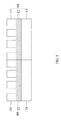
- FIG. 1 is a first schematic view of a three-dimensional integrated circuit in accordance with a first preferred embodiment of the present invention
- FIG. 2 is a second schematic view of a three-dimensional integrated circuit in accordance with the first preferred embodiment of the present invention
- FIG. 3 is a third schematic view of a three-dimensional integrated circuit in accordance with the first preferred embodiment of the present invention.
- FIG. 4 is a fourth schematic view of a three-dimensional integrated circuit in accordance with the first preferred embodiment of the present invention.
- FIG. 5 is a schematic view of a three-dimensional integrated circuit in accordance with a second preferred embodiment of the present invention.
- FIG. 6 is a flow chart of a bonding method for a three-dimensional integrated circuit in accordance with the present invention.
- a first substrate 11 and a second substrate 21 of this preferred embodiment can be silicon wafers of any dimensions or specifications.
- the first film layer 12 or the second film layer 22 can be made of silicon dioxide or any other film material.
- the first metal and the second metal can be any metal, and the first metal of this preferred embodiment can be copper, and the second metal of this preferred embodiment can be titanium, but the invention is not limited to these metals only.
- the first integrated circuit 10 may have a first substrate 11 , a first film layer 12 and a first metal co-deposition layer 13 sequentially.
- the first film layer 12 can be set on the first substrate 11 and made of a material with a thickness that can be changed according to different requirements.
- silicon dioxide with a thickness of 1000 nm is preferably deposited on the first substrate 11 and can be used as the first film layer 12 .
- a light source 1 may be provided to light onto the first film layer 12 to form a graphic structure through a photomask.
- a physical vapor deposition method may be applied for depositing a first metal and a second metal onto the first film layer 12 to form the first metal co-deposition layer 13 .
- the first metal can be copper and the second metal can be titanium, but the invention is not limited to such arrangements only, and the first metal co-deposition layer 13 can be a copper titanium co-deposition structure to form the first integrated circuit 10 .
- a physical vapor deposition method may be a method of using a high-temperature heat source to heat a raw material to a high temperature and vaporize the raw material to form plasma and then condensing the plasma on the substrate to form materials in different states such as single crystal, thin film or crystal grain.
- the second integrated circuit 20 may have a second metal co-deposition layer 23 , a second film layer 22 and a second substrate 21 sequentially, and the second integrated circuit 20 can be superimposed onto the first integrated circuit 10 at a predetermined temperature. It is noteworthy to point out that the first metal co-deposition 13 of the first integrated circuit 10 and the second metal co-deposition 14 of the second integrated circuit 20 are bonded with each other on the contact surface by high temperature process.
- the predetermined temperature preferably may fall within a range from 200° C. to 400° C.
- the first integrated circuit 10 and the second integrated circuit 20 can be bonded to form a three-dimensional integrated circuit.
- first integrated circuit 10 and the second integrated circuit 20 are stacked and bonded with each other in this preferred embodiment, but the invention is not limited to two stacked layers.
- the number of layers and the metal may be used for the manufacture that can be changed freely according to the manufacturing conditions.
- first integrated circuit 10 and the second integrated circuit 20 can be bonded preferably at the predetermined temperature from 200 to 400° C., and an adhesive layer 100 or a barrier layer 200 may be formed near the first film layer 12 and the second film layer 22 .
- first metal co-deposition layer 13 and the second metal co-deposition layer 23 can be a copper titanium co-deposition structure, so that when the first integrated circuit 10 and the second integrated circuit 20 are bonded at the predetermined temperature from 200° C.
- copper atoms will diffuse and move toward the interface, and titanium atoms will move toward the substrate made of silicon dioxide, and a titanium adhesive layer 100 is formed on a surface of the substrate made of silicon dioxide, so as to inhibit copper atoms from diffused into the barrier layer 200 made of silicon dioxide.
- the temperature may be preferably set to a range from 200° C. to 400° C. under atmospheric ambient environment, or a small amount of oxygen is passed into a cavity for bonding the first integrated circuit 10 and the second integrated circuit 20 , and forming a boundary protection layer 300 near a surface of the first metal co-deposition layer 13 and the second metal co-deposition layer 2 .
- titanium tends to be combined with the oxygen in the air to form titanium oxide, so that part of the titanium will move towards the boundary.
- titanium oxide has a very high density, so that once if titanium oxide is formed, oxygen will be unable to diffuse into the copper titanium co-deposition structure. In other words, the diffusion effect can further inhibit copper from being oxidized.
- the present invention further provides a second preferred embodiment for illustrating the invention as follows.
- the first substrate 11 and the third substrate 31 of this preferred embodiment can be silicon wafers with a size or a specification not limited specifically.
- the first film layer 12 or third film layer 32 is made of silicon dioxide or any other film material.
- the first metal and the second metal can be any metal, and the first metal of this preferred embodiment can be copper, and the second metal of this preferred embodiment can be titanium, but the invention is not limited to such arrangements only.
- the first integrated circuit may have a first substrate 11 , a first film layer 12 and a first metal co-deposition layer 13 sequentially.
- the first film layer 12 can be set on the first substrate 11 , and the thickness or material of the first film layer 12 can be changed as needed. In this preferred embodiment, it is preferably to deposit 1000 nm of silicon dioxide on the first substrate 11 as the first film layer 12 . Providing a light source to light onto the first film layer 12 to form a graphic structure through a photomask.
- the physical vapor deposition method can be applied to deposit the first metal and second metal onto the first film layer 12 to form the first metal co-deposition layer 13 .
- the first metal of this preferred embodiment can be copper, and the second metal of this preferred embodiment may be titanium, but the invention is not limited to such arrangements only.
- the first metal co-deposition layer 13 can be a copper titanium co-deposition structure and used for forming the first integrated circuit 10 .
- the third integrated circuit 40 can be manufactured by the same stacking and manufacturing method of the first integrated circuit 10 , and the third integrated circuit 40 may have a third substrate 31 , a third film layer 32 and a third metal co-deposition layer 33 sequentially.
- the first integrated circuit 10 can be attached on a side of the third integrated circuit 40 at a predetermined temperature, and the temperature preferably falls within a range from 200° C. to 400° C.
- the first integrated circuit 10 and the third integrated circuit 40 are attached and bonded side by side with each other, but the invention is not limited to such arranged positions only.
- the bonding method is applicable for manufacturing a three-dimensional integrated circuit, and the three-dimensional integrated circuit comprises a first integrated circuit and a second integrated circuit.
- the first integrated circuit may have a first substrate, a first film layer and a first metal co-deposition layer sequentially
- the second integrated circuit may have a second metal co-deposition layer, a second film layer and a second substrate sequentially.
- the bonding method for a three-dimensional integrated circuit comprising the following steps:
- Step S 11 Providing a substrate.
- Step S 12 Depositing a film layer on the substrate.
- Step S 13 Providing a light source to light onto the film layer to form a graphic structure.
- Step S 14 Forming a metal co-deposition layer on the film layer by a first metal and a second metal.
- Step S 15 Providing a first integrated circuit sequentially having a substrate, a film layer and a metal co-deposition layer.
- Step S 16 Providing a second integrated circuit sequentially having a metal co-deposition layer, a film layer and a substrate.
- Step S 17 Superimposing the first integrated circuit on the second integrated circuit under atmospheric ambient environment or a cavity which has a small amount of oxygen at a predetermined temperature.
- the bonding method for a three-dimensional integrated circuit and the three-dimensional integrated circuit in accordance with the present invention have one or more of the following advantages:
- the present invention can overcome the problems of the prior art having a complicated manufacturing process, failing to extend the degree of freedom, and limiting the development of science and technology.
- the bonding method for a three-dimensional integrated circuit and the three-dimensional integrated circuit in accordance with the present invention can be applied in the high-temperature manufacturing process for bonding copper and titanium under atmospheric ambient environment and automatically forming a titanium adhesive layer, a barrier layer and a boundary protection layer made of titanium oxide for resisting the oxidization of copper.
- the bonding method for a three-dimensional integrated circuit and the three-dimensional integrated circuit in accordance with the present invention can simplify the manufacturing flow and form a copper titanium co-deposition structure directly without increasing an additional sputter deposition of a titanium adhesive layer, a copper seed layer or a mass copper layer.
Abstract
Description
Claims (9)
Applications Claiming Priority (3)
| Application Number | Priority Date | Filing Date | Title |
|---|---|---|---|
| TW100133482 | 2011-09-16 | ||
| TW100133482A TWI433268B (en) | 2011-09-16 | 2011-09-16 | Bonding method for three-dimensional integrated circuit and three-dimensional integrated circuit thereof |
| TW100133482A | 2011-09-16 |
Publications (2)
| Publication Number | Publication Date |
|---|---|
| US20130069248A1 US20130069248A1 (en) | 2013-03-21 |
| US8508041B2 true US8508041B2 (en) | 2013-08-13 |
Family
ID=47879922
Family Applications (1)
| Application Number | Title | Priority Date | Filing Date |
|---|---|---|---|
| US13/325,587 Active - Reinstated 2032-02-27 US8508041B2 (en) | 2011-09-16 | 2011-12-14 | Bonding method for three-dimensional integrated circuit and three-dimensional integrated circuit thereof |
Country Status (3)
| Country | Link |
|---|---|
| US (1) | US8508041B2 (en) |
| KR (1) | KR101384131B1 (en) |
| TW (1) | TWI433268B (en) |
Families Citing this family (2)
| Publication number | Priority date | Publication date | Assignee | Title |
|---|---|---|---|---|
| CN104465428B (en) * | 2013-09-16 | 2017-10-13 | 中国科学院上海微系统与信息技术研究所 | A kind of method of copper copper metal thermocompression bonding |
| CN113718206B (en) * | 2021-08-23 | 2023-03-07 | 中山市气相科技有限公司 | Preparation method of TaTiN multilayer film with sandwich structure and film |
Citations (6)
| Publication number | Priority date | Publication date | Assignee | Title |
|---|---|---|---|---|
| US5334804A (en) | 1992-11-17 | 1994-08-02 | Fujitsu Limited | Wire interconnect structures for connecting an integrated circuit to a substrate |
| US6890829B2 (en) * | 2000-10-24 | 2005-05-10 | Intel Corporation | Fabrication of on-package and on-chip structure using build-up layer process |
| US7239025B2 (en) * | 1999-02-19 | 2007-07-03 | Micron Technology, Inc. | Selective deposition of solder ball contacts |
| US7335994B2 (en) * | 2003-01-27 | 2008-02-26 | Micron Technology, Inc. | Semiconductor component having multiple stacked dice |
| US7497005B2 (en) * | 1999-02-03 | 2009-03-03 | Micron Technology, Inc. | Method for forming an inductor |
| US7932590B2 (en) * | 2006-07-13 | 2011-04-26 | Atmel Corporation | Stacked-die electronics package with planar and three-dimensional inductor elements |
Family Cites Families (1)
| Publication number | Priority date | Publication date | Assignee | Title |
|---|---|---|---|---|
| US7402509B2 (en) * | 2005-03-16 | 2008-07-22 | Intel Corporation | Method of forming self-passivating interconnects and resulting devices |
-
2011
- 2011-09-16 TW TW100133482A patent/TWI433268B/en not_active IP Right Cessation
- 2011-12-14 US US13/325,587 patent/US8508041B2/en active Active - Reinstated
-
2012
- 2012-02-03 KR KR1020120011321A patent/KR101384131B1/en active IP Right Grant
Patent Citations (6)
| Publication number | Priority date | Publication date | Assignee | Title |
|---|---|---|---|---|
| US5334804A (en) | 1992-11-17 | 1994-08-02 | Fujitsu Limited | Wire interconnect structures for connecting an integrated circuit to a substrate |
| US7497005B2 (en) * | 1999-02-03 | 2009-03-03 | Micron Technology, Inc. | Method for forming an inductor |
| US7239025B2 (en) * | 1999-02-19 | 2007-07-03 | Micron Technology, Inc. | Selective deposition of solder ball contacts |
| US6890829B2 (en) * | 2000-10-24 | 2005-05-10 | Intel Corporation | Fabrication of on-package and on-chip structure using build-up layer process |
| US7335994B2 (en) * | 2003-01-27 | 2008-02-26 | Micron Technology, Inc. | Semiconductor component having multiple stacked dice |
| US7932590B2 (en) * | 2006-07-13 | 2011-04-26 | Atmel Corporation | Stacked-die electronics package with planar and three-dimensional inductor elements |
Non-Patent Citations (1)
| Title |
|---|
| Tsukimoto, S. et al. "Effect of Annealing Ambient on the Self-Formation Mechanism of Diffusion Barrier Layers Used in Cu(Ti) Interconnects" Journal of Electronic Materials, 2007, 36(3):258-265. |
Also Published As
| Publication number | Publication date |
|---|---|
| US20130069248A1 (en) | 2013-03-21 |
| KR101384131B1 (en) | 2014-04-10 |
| TWI433268B (en) | 2014-04-01 |
| KR20130030182A (en) | 2013-03-26 |
| TW201314838A (en) | 2013-04-01 |
Similar Documents
| Publication | Publication Date | Title |
|---|---|---|
| TWI536525B (en) | Chip package | |
| TWI706519B (en) | Semiconductor package having routable encapsulated conductive substrate and method | |
| US8310050B2 (en) | Electronic device package and fabrication method thereof | |
| US7825504B2 (en) | Semiconductor package and multi-chip semiconductor package using the same | |
| TWI614815B (en) | Bendable and stretchable electronic devices and methods | |
| US9064862B2 (en) | Semiconductor chips having a dual-layered structure, packages having the same, and methods of fabricating the semiconductor chips and the packages | |
| US20150255499A1 (en) | Chip package and method of fabricating the same | |
| TW201133727A (en) | Chip package and fabrication method thereof | |
| TW201405735A (en) | Grid fan-out wafer level package and methods of manufacturing a grid fan-out wafer level package | |
| TW200919632A (en) | Through-silicon vias and methods for forming the same | |
| CN103295978A (en) | Semiconductor package and fabrication method thereof | |
| US20200411405A1 (en) | Semiconductor package | |
| TWI335069B (en) | Ic chip component, multi chip module, integrated structure thereof and method for manufacturing them | |
| JP2000100847A (en) | Semiconductor device and manufacture thereof | |
| TWI500090B (en) | Method of forming semiconductor package | |
| JP2012256951A (en) | Semiconductor package, laminated wafer level package having the same and laminated wafer level package manufacturing method | |
| JP6300301B2 (en) | Semiconductor device and manufacturing method of semiconductor device | |
| CN103681533A (en) | Fan-out package comprising bulk metal | |
| US8508041B2 (en) | Bonding method for three-dimensional integrated circuit and three-dimensional integrated circuit thereof | |
| TW201135907A (en) | Integrated circuit package system with offset stacked die | |
| CN107369695A (en) | Wafer encapsulation body and its manufacture method | |
| US11445617B2 (en) | Package structure and manufacturing method thereof | |
| TWI818419B (en) | Manufacturing method of package structure of electronic device | |
| US11749646B2 (en) | Semiconductor package and manufacturing method thereof | |
| JP6986221B2 (en) | Manufacturing method of hole electrode substrate, hole electrode substrate and semiconductor device |
Legal Events
| Date | Code | Title | Description |
|---|---|---|---|
| AS | Assignment |
Owner name: NATIONAL CHIAO TUNG UNIVERSITY, TAIWAN Free format text: ASSIGNMENT OF ASSIGNORS INTEREST;ASSIGNORS:CHEN, KUAN-NENG;HSU, SHENG-YAO;REEL/FRAME:027395/0361 Effective date: 20110906 |
|
| STCF | Information on status: patent grant |
Free format text: PATENTED CASE |
|
| FPAY | Fee payment |
Year of fee payment: 4 |
|
| FEPP | Fee payment procedure |
Free format text: MAINTENANCE FEE REMINDER MAILED (ORIGINAL EVENT CODE: REM.); ENTITY STATUS OF PATENT OWNER: SMALL ENTITY |
|
| LAPS | Lapse for failure to pay maintenance fees |
Free format text: PATENT EXPIRED FOR FAILURE TO PAY MAINTENANCE FEES (ORIGINAL EVENT CODE: EXP.); ENTITY STATUS OF PATENT OWNER: SMALL ENTITY |
|
| STCH | Information on status: patent discontinuation |
Free format text: PATENT EXPIRED DUE TO NONPAYMENT OF MAINTENANCE FEES UNDER 37 CFR 1.362 |
|
| FP | Lapsed due to failure to pay maintenance fee |
Effective date: 20210813 |
|
| PRDP | Patent reinstated due to the acceptance of a late maintenance fee |
Effective date: 20211112 |
|
| FEPP | Fee payment procedure |
Free format text: PETITION RELATED TO MAINTENANCE FEES FILED (ORIGINAL EVENT CODE: PMFP); ENTITY STATUS OF PATENT OWNER: SMALL ENTITY Free format text: PETITION RELATED TO MAINTENANCE FEES GRANTED (ORIGINAL EVENT CODE: PMFG); ENTITY STATUS OF PATENT OWNER: SMALL ENTITY Free format text: SURCHARGE, PETITION TO ACCEPT PYMT AFTER EXP, UNINTENTIONAL. (ORIGINAL EVENT CODE: M2558); ENTITY STATUS OF PATENT OWNER: SMALL ENTITY |
|
| MAFP | Maintenance fee payment |
Free format text: PAYMENT OF MAINTENANCE FEE, 8TH YR, SMALL ENTITY (ORIGINAL EVENT CODE: M2552); ENTITY STATUS OF PATENT OWNER: SMALL ENTITY Year of fee payment: 8 |
|
| STCF | Information on status: patent grant |
Free format text: PATENTED CASE |
|
| AS | Assignment |
Owner name: NATIONAL YANG MING CHIAO TUNG UNIVERSITY, TAIWAN Free format text: MERGER AND CHANGE OF NAME;ASSIGNORS:NATIONAL CHIAO TUNG UNIVERSITY;NATIONAL YANG MING UNIVERSITY;REEL/FRAME:058237/0138 Effective date: 20210201 |
|
| AS | Assignment |
Owner name: HANNSTAR DISPLAY CORPORATION, TAIWAN Free format text: ASSIGNMENT OF ASSIGNORS INTEREST;ASSIGNOR:NATIONAL YANG MING CHIAO TUNG UNIVERSITY;REEL/FRAME:058532/0268 Effective date: 20211213 |
|
| FEPP | Fee payment procedure |
Free format text: ENTITY STATUS SET TO UNDISCOUNTED (ORIGINAL EVENT CODE: BIG.); ENTITY STATUS OF PATENT OWNER: LARGE ENTITY |