US8539409B1 - Simultaneous development of complementary IC families - Google Patents
Simultaneous development of complementary IC families Download PDFInfo
- Publication number
- US8539409B1 US8539409B1 US13/178,599 US201113178599A US8539409B1 US 8539409 B1 US8539409 B1 US 8539409B1 US 201113178599 A US201113178599 A US 201113178599A US 8539409 B1 US8539409 B1 US 8539409B1
- Authority
- US
- United States
- Prior art keywords
- family
- ics
- masks
- different
- value
- Prior art date
- Legal status (The legal status is an assumption and is not a legal conclusion. Google has not performed a legal analysis and makes no representation as to the accuracy of the status listed.)
- Active, expires
Links
Images


Classifications
-
- G—PHYSICS
- G06—COMPUTING; CALCULATING OR COUNTING
- G06F—ELECTRIC DIGITAL DATA PROCESSING
- G06F30/00—Computer-aided design [CAD]
- G06F30/30—Circuit design
- G06F30/34—Circuit design for reconfigurable circuits, e.g. field programmable gate arrays [FPGA] or programmable logic devices [PLD]
Definitions
- the present invention relates to integrated circuits, and, more specifically but not exclusively, to the processes of designing, testing, and qualifying of families of integrated circuits, such as field-programmable gate arrays (FPGAs).
- FPGAs field-programmable gate arrays
- ICs integrated circuits
- handheld electronic devices typically require integrated circuits having a low standby power level in order to conserve the limited amount of battery power available
- computer servers typically require integrated circuits having a high speed in order to achieve required levels of processing and throughput.
- the standard approach to developing ICs for low-power applications and ICs for high-speed applications is to implement completely independent design, test, and qualification processes, one unique process for each different application.
- a family of multiple, different ICs may be developed for each different application, but the different families are developed separately from one another.
- Within an IC family there is typically a lead IC and one or more follow-on ICs that differ from the lead IC in floorplan, size, and content, but use a common set of circuits and blocks.
- Some sharing of internal blocks, like PLL (phase-locked loop) or memory blocks or IO (input/output), between different IC families may be implemented, but the floorplan, top layout, verification, assembly, test, QA (quality assurance), and reliability for the different families follow from separate development efforts.
- PLL phase-locked loop
- IO input/output
- two or more different, but complementary families of ICs can be developed simultaneously within a common framework such that block-level layouts, top-level device layouts, top-level assembly procedures, test benches, ATE (automatic test equipment) test vectors, pinout, packages, verification scripts, reliability testing, ESD (electro-static discharge), etc., may all be shared and developed in common.
- the present invention is a method for making at least first and second families of integrated circuits (ICs), wherein the first family has performance characteristics different from the second family, the method comprising (a) providing a common layout for the at least first and second families; (b) specifying a first value for a first IC design parameter, such that one or more ICs of the first family are fabricated based on the first selected value for the first IC design parameter; and (c) specifying a second value, different from the first value, for the first IC design parameter, such that one or more ICs of the second family are fabricated based on the second selected value for the first IC design parameter, wherein the one or more ICs of the first family have the common layout but performance characteristics different from the one or more ICs of the second family.
- ICs integrated circuits
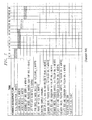
- FIG. 1 presents Table I, which identifies the tasks involved in an exemplary development of IC families
- FIG. 2 shows an exemplary timeline for the conventional development of a single IC family
- FIG. 3 shows an exemplary timeline for the conventional, independent development of two different IC families
- FIG. 4 shows a corresponding exemplary timeline for the simultaneous development of two different, but complementary IC families analogous to the two IC families of FIG. 3 ;
- FIG. 5 presents an exemplary, high-level flow diagram of some of the processing involved in simultaneously developing two complementary IC families.
- Vt threshold voltage
- Vt threshold voltage
- the Vt level of a transistor can be selected by designing the transistor to have an appropriate type and amount of dopant.
- the term “layout” refers to the geometry and artwork comprising the levels and mask layers that define the physical implementation of the transistors, implants, wires, guardrings, vias, contacts, etc., that make up the physical view of the circuits.
- two IC families can be designed to have the same, or common, layout, where, in the first family, a number of transistors have relatively high Vt levels, while the corresponding transistors in the second family have relatively low Vt levels.
- the set of masks used to fabricate the first family of ICs can be substantially identical to the set of masks used to fabricate the second family of ICs, where the two sets of masks might differ by only a very small number of masks (e.g., one to five masks) that are associated with achieving the different Vt levels.
- Controlling the Vt level is just one way of achieving different, specific operating characteristics at the transistor level and thereby different, overall operating characteristics at the IC level.
- Other variable design parameters include, without limitation, the thickness of the transistor gate oxide (where thicker implies lower power and lower speed), the length of the transistor channel (where longer implies lower power and lower speed), the type of pocket implant, and the type of extension implant.
- relatively low Vt levels can be achieved using a pocket implant of In+ (Indium) and an extension implant of As+ (Arsenic), while relatively high Vt levels can be achieved using a pocket implant of B+ (Boron) and an extension implant of P+/As+ (Phosphorus/Arsenic combination).
- the Phosphorus extension helps to achieve a high-Vt device.
- channel length is a variable design parameter
- the common layout for the different IC families would be designed to accommodate the longest of the channel lengths at play, where the poly level that defines the transistor channel length for each family would be excluded from the term “common layout.”
- the slow speed/low power family may use a channel length of 70 nm
- the high performance/high power family may use 60 nm channel lengths.
- the circuit layouts would be executed to the larger of the two dimensions, i.e., 70 nm, and all layout design rules verified and satisfied against the 70 nm rule.
- a comparable CAD Computer-Aided Design
- the low-power circuit- may use longer, smaller (i.e., narrower) transistors with high Vt implants, while the high-performance circuit-may use shorter channel length, physically wider transistors with low Vt activation levels for high Idsat drive strength and speed.
- the typical practice is to employ fully the transistor length, width, and circuit design changes, resulting in unique layouts, and a more serial approach to design, fabrication, test, and verification.
- physical layouts reflect the design differences resulting in two very distinct layouts having little in common, except for potentially being logically identical.
- Certain embodiments of the present invention limit normal design practice to only Vt changes, enforcing a common layout for all other design parameters that normally would be fully optimized. This produces a near common mask set, saving substantially the mask set costs. It also enforces a design requirement for simultaneous design of both families leading to an overall reduction in project costs and time to market. Designing, testing, qualifying, and verifying two IC families to serve two distinct market segments simultaneously, reduces development costs, improves time to market, and broadens each IC family's market penetration. This is achieved by enforcing the restriction of common layout limited solely to change of implant between IC families which is not normal practice for IC design.
- Vt-only mask changes provided a common layout principle is followed and the CAD (computer-aided design) flow is designed appropriately to support the Vt switch.
- the invention enables cost savings in mask set costs as well as development costs due to collapsed, parallel development efforts resulting in reduced development schedules.
- a first, low-power family of ICs and a second, high-speed family of ICs are developed simultaneously such that the two different, but complementary families have the same layout and share most of the same masks used in fabricating the ICs of the two different families.
- handheld devices require standby currents in the nano-amp to micro-amp range as a primary system requirement, while typically having reduced internal speed requirements.
- servers require much faster internal speeds but allow for several orders of magnitude higher standby currents.
- FIG. 1 presents Table I, which identifies the tasks involved in an exemplary development of IC families with a comparison of the typical amount of time that it takes for each of the tasks when developing a single family of ICs vs. the simultaneous development of two complementary families of ICs: one for low-power applications and one for high-speed applications.
- certain tasks e.g., block design, block layout, and IC assembly and verification
- take longer when simultaneously developing two complementary IC families than for a single IC family because of the restriction to use implant-only changes to meet different market objectives placed on the IC designer.
- FIG. 2 shows an exemplary timeline for the conventional development of a single IC family having four different ICs in the family: a lead IC and three follow-on ICs. Note that certain tasks can overlap in time.
- phase one testing and validation (Task 6 ) of the lead IC can be implemented during the wafer fabrication processing of the first mask order (Task 5 ) for the lead chip.
- first mask order Task 5
- the wafer processing (Task 10 ) for the mask order for the second follow-on IC can be performed during the testing and validation (Task 11 ) for the first follow-on IC and can even be started to overlap with the tail end of the wafer processing (Task 10 ) for the second follow-on device.
- the full family of ICs are ready for production after a total development time of 40 months.
- FIG. 3 shows an exemplary timeline for the conventional, independent development of two different IC families, each having four different ICs in the family.
- the development of the second family can be initiated before the completion of the development of the first family.
- the specification writing (Task 1 ) for the second family can begin during the wafer fabrication processing for the first mask order (Task 5 ) for the first family.
- the first full family of ICs are ready for production after the same 40-month development time as in FIG. 2 , while both full families of ICs are not ready for production until after a total development time of 61 months.
- FIG. 4 shows a corresponding exemplary timeline for the simultaneous development of two different, but complementary IC families analogous to the two IC families of FIG. 3 , each family having four different chips.
- certain tasks e.g., Tasks 2 , 3 , and 4
- the overall development time for both full families of ICs is only 44 months, a significant 17-month reduction in development time as compared to the conventional 61-month duration of FIG. 3 .
- Project costs typically align with project development time.
- both families are developed within a common framework such that block-level layouts, top-level device layouts, top-level assembly procedures, test benches, ATE test vectors, pinout, packages, verification scripts, reliability testing, ESD, etc., may all be shared and developed in common.
- the layouts and various components of the development framework are common with the exception of the mask layers that define the implant layers used to define those Vt levels.
- These implant layers may be referred to as “dual implant” layers, where, in a low-power device, the core transistor implants are set to high Vt for low-power, but low-speed transistor types, while, in a complementary, high-speed device, the core transistor implants are set to low Vt for high-speed, but high-power transistor types. Hence, they are dual mode implants.
- the implant mask levels are set appropriately to achieve the desired speed/power customization.
- the personalization of the entire IC is managed by an implant switch implemented in the CAD (computer-aided design) flow and transistor models.
- CAD computer-aided design
- the global switch between low-power transistors and high-speed transistors modifies the nature of the entire device and the market segment it serves.
- the transistor implant defines the transistor's Vt and Idsat (saturation current) behavior defining the speed/power for that specific transistor.
- Dual implant technology applies a principle of switching implants across an entire IC based on a global switch in the mask realization process. This implies that, for the low-power devices, these transistors will be defined to be the high-Vt, low-power implant transistor type, while, for high-speed products, the dual implant tagged transistors will be defined to be the low-Vt, high-speed implant transistor type.
- the entire chip's system performance is defined by the implant change, not just at the subcircuit level. Because the entire IC system behavior is impacted, all timing simulations and system verification must comprehend the dual implant nature of the timing and power from the beginning of product development in a complete, chip-level context. For instance, circuits critical to speed are fully simulated under both implant options to verify performance metrics such as jitter, duty cycle, switching points, stability, intrinsic delay, extrinsic delay, etc., using both implant options and in the context of the entire IC switching its implant nature from low power to high speed.
- the IC designers through transistor models simulate the implant switch of the entire device as a system and verify that the system timing and power of the IC meet the specific needs of the market requirement.
- the CAD flow, the up-front simulation of both environments, and the system-level analysis of the context switch are important differentiations of the development flow on the front end.
- the implant change is across major portions of the chip, creating in effect a new product class, but only when designed up front to be consistent within itself and within the system requirements for each product.
- FIG. 5 presents an exemplary, high-level flow diagram of some of the processing involved in simultaneously developing two complementary IC families, in which the first family consists of low-power ICs and the second family consists of high-speed chips, where complementary ICs in different families differ only in the Vt levels of at least some of their transistors.
- steps 502 - 512 may be implemented using conventional CAD tools running on a computer, where different appropriate tools may be needed to implement particular steps, while step 514 - 520 may be implemented at a semiconductor fabrication facility.
- steps 502 and 504 the different sets of requirements are specified for the first and second families, respectively.
- the requirements for the first (low-power) family would include, among other requirements, appropriate low-power constraints
- the requirements for the second (high-speed) family would include, among other requirements, appropriate high-speed constraints.
- step 506 based on the two different sets of requirements for the two different families, a common IC layout is designed, and the Vt levels are specified for each transistor in each family.
- step 508 simulations are performed for both families based on the common IC layout and the respective, differing Vt levels.
- step 510 the simulations indicate that both families do not satisfy their respective sets of requirements, then the requirements for one or both of the families are possibly modified in step 512 , and the Vt levels and/or the layout itself are modified in step 506 based on the modified requirements.
- the modified designs for the two families are then re-simulated in step 508 and re-evaluated in step 510 . This iterative process of modifying requirements and designs followed by re-simulating and re-evaluating the modified designs is repeated until both families pass their respective sets of requirements in step 510 .
- the resulting common layout with different Vt levels for the two different families is represented by four different subsets of masks used to fabricate the ICs of the two different families: a common initial subset of masks that is used for both families, a unique intermediate subset of masks that is used only for the first family, a different, unique intermediate subset of masks that is used only for the second family, and a common final subset of masks that is used to both families.
- the application of these four subsets of masks is reflected in FIG. 5 as follows.
- step 514 the common initial subset of masks is applied for all ICs of both families to produce identical partially fabricated ICs for both families.
- step 516 the unique intermediate subset of masks is applied to just the partially fabricated ICs from step 514 for the first family to produce partially fabricated ICs having the higher Vt levels, while, in step 518 , the different, unique intermediate subset of masks is applied to just the partially fabricated ICs from step 514 for the second family to produce partially fabricated ICs having the lower Vt levels.
- step 520 the common final subset of masks is applied to all partially fabricated ICs from steps 516 and 518 to produce the completed ICs for both families.
- the number of masks in the two different, unique, intermediate subsets for the two families may be the same or different, including the possibility that one of the intermediate subsets is empty. This might result, for example, from a situation in which one IC family is fabricated using a particular dopant level to achieve its Vt level, while the other IC family achieves its Vt level without any doping. In that case, the latter family's unique subset of masks may be empty.
- a combination (“combo”) reticle can be fabricated in which different dice of the reticle are assigned to different members of the different families.
- a reticle as referenced here is an X by Y matrix of ICs that are simultaneously processed during the fabrication process and is common practice in the semiconductor fabrication field.
- This “combo” reticle is stepped across the entire wafer as it is fabricated and can provide all the versions of the product on the same wafer. As a result, this reduces the number of wafers that need to be fabricated (and the corresponding cost) since all products are fabricated at the same time and available at the same time.
- a regulated device can use external voltages from 1.8V to 3.6V, while controlling the internal voltage on the device to 1.2V.
- An un-regulated version of the product would use only an external voltage of 1.2V. This option is can be ‘optioned’ in or out with a metal mask.
- each version or family of the product has its own unique set of product parameters that are verified as functional and meeting some specific set of requirements.
- a single testing sort flow test program cannot be used as is the normal practice in the semiconductor industry.
- a means of uniquely identifying each family member of the product has been developed in order to dynamically select the appropriate different set of tests for each unique version of the product.
- One possible method is to have internal ‘hardwired’ bits in the product that can be read from the device. These bits uniquely identify not only the product type but also the correct voltage to be used for the family in order to function properly, even when an improper voltage level may be currently applied.
- One means of accomplishing this can be to have the hardwired bits always require a ‘transition’ state to be valid. For example, a sequence of 4 bits of all “1”s or all “0”s would not be a valid state, while any other sequence of bits would indicate a potential valid stated (e.g., “1011” could be valid).
- the establishment of all “1”s or all “0”s as invalid states is to prevent a failing IC with stuck high or low bits being recognized as valid. Alternating bits indicate a somewhat functional IC.
- the present invention has been described in the context of two IC families having four ICs each, the invention is not so limited. In general, the present invention can be applied to two or more different, but complementary IC families, where each family has one or more ICs and where different families may have the same or different numbers of ICs as other families. For example, in addition to a low-power family and a high-speed family, there may be one or more other families having intermediate levels of power and speed achieved using transistors having intermediate Vt levels.
- ASICs application-specific integrated circuits
- FPGAs field-programmable gate arrays
- PLDs programmable logic devices
- MPGAs mask-programmable gate arrays
- SPLDs simple programmable logic devices
- CPLDs complex programmable logic devices
- any block diagrams herein represent conceptual views of illustrative circuitry embodying the principles of the invention.
- any flow charts, flow diagrams, state transition diagrams, pseudo code, and the like represent various processes which may be substantially represented in computer readable medium and so executed by a computer or processor, whether or not such computer or processor is explicitly shown.
- each numerical value and range should be interpreted as being approximate as if the word “about” or “approximately” preceded the value of the value or range.
- figure numbers and/or figure reference labels in the claims is intended to identify one or more possible embodiments of the claimed subject matter in order to facilitate the interpretation of the claims. Such use is not to be construed as necessarily limiting the scope of those claims to the embodiments shown in the corresponding figures.
Abstract
Description
-
- 1) Apply the lowest common voltage for an unregulated device (e.g., 1.2V) and attempt to read a valid sequence of bits from the device.
- a. If a valid sequence is found,
- i. This means that the device is an unregulated device.
- ii. Branch to the testing software appropriately for that product version.
- b. If an invalid sequence is read, go to
step 2.
- a. If a valid sequence is found,
- 2) Apply the next highest level of voltage (for a regulated device) to the device and attempt to read a valid sequence of bits from the device.
- a. If a valid sequence is found,
- i. This means that the device is a regulated device.
- ii. Branch to the testing software appropriately for that product version.
- b. If an invalid sequence is read, go to
step 3.
- a. If a valid sequence is found,
- 3) Device fails to read a valid ID for either regulated or unregulated versions of the device and thus is a failing IC and should be discarded.
- 1) Apply the lowest common voltage for an unregulated device (e.g., 1.2V) and attempt to read a valid sequence of bits from the device.
Claims (25)
Priority Applications (1)
| Application Number | Priority Date | Filing Date | Title |
|---|---|---|---|
| US13/178,599 US8539409B1 (en) | 2011-07-08 | 2011-07-08 | Simultaneous development of complementary IC families |
Applications Claiming Priority (1)
| Application Number | Priority Date | Filing Date | Title |
|---|---|---|---|
| US13/178,599 US8539409B1 (en) | 2011-07-08 | 2011-07-08 | Simultaneous development of complementary IC families |
Publications (1)
| Publication Number | Publication Date |
|---|---|
| US8539409B1 true US8539409B1 (en) | 2013-09-17 |
Family
ID=49122545
Family Applications (1)
| Application Number | Title | Priority Date | Filing Date |
|---|---|---|---|
| US13/178,599 Active 2031-10-14 US8539409B1 (en) | 2011-07-08 | 2011-07-08 | Simultaneous development of complementary IC families |
Country Status (1)
| Country | Link |
|---|---|
| US (1) | US8539409B1 (en) |
Citations (12)
| Publication number | Priority date | Publication date | Assignee | Title |
|---|---|---|---|---|
| US5693540A (en) * | 1996-04-03 | 1997-12-02 | Altera Corporation | Method of fabricating integrated circuits |
| US5783846A (en) * | 1995-09-22 | 1998-07-21 | Hughes Electronics Corporation | Digital circuit with transistor geometry and channel stops providing camouflage against reverse engineering |
| US6406980B1 (en) | 2000-08-24 | 2002-06-18 | International Business Machines Corporation | Physical design technique providing single and multiple core microprocessor chips in a single design cycle and manufacturing lot using shared mask sets |
| US6472926B2 (en) * | 2000-07-18 | 2002-10-29 | Mitsubishi Denki Kabushiki Kaisha | Internal voltage generation circuit |
| US6475850B2 (en) | 1996-01-16 | 2002-11-05 | Micron Technology, Inc. | Bipolar-CMOS (BiCMOS) process for fabricating integrated circuits |
| US6922823B2 (en) * | 2002-12-13 | 2005-07-26 | Lsi Logic Corporation | Method for creating derivative integrated circuit layouts for related products |
| US7137092B2 (en) * | 2003-08-21 | 2006-11-14 | Kawasaki Microelectronics, Inc. | Layout method of semiconductor integrated circuit, layout structure thereof, and photomask for forming the layout structure |
| US7402482B2 (en) | 2004-03-26 | 2008-07-22 | Atmel Corporation | Non-volatile transistor memory array incorporating read-only elements with single mask set |
| US7844923B2 (en) * | 2006-10-20 | 2010-11-30 | Panasonic Corporation | Semiconductor integrated circuit designing method, semiconductor integrated circuit device, and electronic device |
| US8151224B1 (en) | 2008-12-29 | 2012-04-03 | Altera Corporation | Method of designing integrated circuits including providing an option to select a mask layer set |
| US20120131533A1 (en) * | 2010-11-18 | 2012-05-24 | Stmicroelectronics (Rousset) Sas | Method of fabricating an integrated circuit protected against reverse engineering |
| US8200233B2 (en) * | 2007-09-21 | 2012-06-12 | Samsung Electronics Co., Ltd. | Apparatus and method for supporting cells with different characteristics in a broadband wireless communication system |
-
2011
- 2011-07-08 US US13/178,599 patent/US8539409B1/en active Active
Patent Citations (12)
| Publication number | Priority date | Publication date | Assignee | Title |
|---|---|---|---|---|
| US5783846A (en) * | 1995-09-22 | 1998-07-21 | Hughes Electronics Corporation | Digital circuit with transistor geometry and channel stops providing camouflage against reverse engineering |
| US6475850B2 (en) | 1996-01-16 | 2002-11-05 | Micron Technology, Inc. | Bipolar-CMOS (BiCMOS) process for fabricating integrated circuits |
| US5693540A (en) * | 1996-04-03 | 1997-12-02 | Altera Corporation | Method of fabricating integrated circuits |
| US6472926B2 (en) * | 2000-07-18 | 2002-10-29 | Mitsubishi Denki Kabushiki Kaisha | Internal voltage generation circuit |
| US6406980B1 (en) | 2000-08-24 | 2002-06-18 | International Business Machines Corporation | Physical design technique providing single and multiple core microprocessor chips in a single design cycle and manufacturing lot using shared mask sets |
| US6922823B2 (en) * | 2002-12-13 | 2005-07-26 | Lsi Logic Corporation | Method for creating derivative integrated circuit layouts for related products |
| US7137092B2 (en) * | 2003-08-21 | 2006-11-14 | Kawasaki Microelectronics, Inc. | Layout method of semiconductor integrated circuit, layout structure thereof, and photomask for forming the layout structure |
| US7402482B2 (en) | 2004-03-26 | 2008-07-22 | Atmel Corporation | Non-volatile transistor memory array incorporating read-only elements with single mask set |
| US7844923B2 (en) * | 2006-10-20 | 2010-11-30 | Panasonic Corporation | Semiconductor integrated circuit designing method, semiconductor integrated circuit device, and electronic device |
| US8200233B2 (en) * | 2007-09-21 | 2012-06-12 | Samsung Electronics Co., Ltd. | Apparatus and method for supporting cells with different characteristics in a broadband wireless communication system |
| US8151224B1 (en) | 2008-12-29 | 2012-04-03 | Altera Corporation | Method of designing integrated circuits including providing an option to select a mask layer set |
| US20120131533A1 (en) * | 2010-11-18 | 2012-05-24 | Stmicroelectronics (Rousset) Sas | Method of fabricating an integrated circuit protected against reverse engineering |
Similar Documents
| Publication | Publication Date | Title |
|---|---|---|
| US7127687B1 (en) | Method and apparatus for determining transistor sizes | |
| US7784012B2 (en) | System and method for creating a standard cell library for use in circuit designs | |
| US7675317B2 (en) | Integrated circuits with adjustable body bias and power supply circuitry | |
| US20230274060A1 (en) | Automated circuit generation | |
| US8316339B2 (en) | Zone-based leakage power optimization | |
| JP2000305961A (en) | Cell library database and design assisting device | |
| US20170308639A1 (en) | Method for analyzing ir drop and electromigration of ic | |
| US8255859B2 (en) | Method and system for verification of multi-voltage circuit design | |
| US20080040091A1 (en) | Method and apparatus of simulating a semiconductor integrated circuit at gate level | |
| US20220327275A1 (en) | Multiplexer | |
| US20050216872A1 (en) | Method to design and verify an integrated circuit device with multiple power domains | |
| US7062739B2 (en) | Gate reuse methodology for diffused cell-based IP blocks in platform-based silicon products | |
| US8539409B1 (en) | Simultaneous development of complementary IC families | |
| US11368158B2 (en) | Methods for handling integrated circuit dies with defects | |
| US6148434A (en) | Apparatus and method for minimizing the delay times in a semiconductor device | |
| KR100772269B1 (en) | Design method of mtcmos semiconductor integrated circuit | |
| US8843870B2 (en) | Method of reducing current leakage in a device and a device thereby formed | |
| US7451413B1 (en) | Methods of minimizing leakage current by analyzing post layout information and associated threshold voltage and leakage current | |
| US9569570B2 (en) | Configurable delay cell | |
| US9553581B2 (en) | Package-aware state-based leakage power reduction | |
| US11876516B2 (en) | Non-fighting level shifters | |
| US7093217B1 (en) | Method and apparatus for determining the optimal fanout across a logic element | |
| US20230106989A1 (en) | Method of verifying semiconductor device, method of designing and manufacturing semiconductor device using the same, and system performing the same | |
| US9104825B1 (en) | Method of reducing current leakage in a product variant of a semiconductor device | |
| US11621704B2 (en) | Input Schmitt buffer operating at a high voltage using low voltage devices |
Legal Events
| Date | Code | Title | Description |
|---|---|---|---|
| AS | Assignment |
Owner name: LATTICE SEMICONDUCTOR CORPORATION, OREGON Free format text: ASSIGNMENT OF ASSIGNORS INTEREST;ASSIGNORS:SCHADT, JOHN;FONG, STEVEN J.;MURRAY, SHAWN;AND OTHERS;SIGNING DATES FROM 20110624 TO 20110707;REEL/FRAME:026560/0944 |
|
| FEPP | Fee payment procedure |
Free format text: PAYOR NUMBER ASSIGNED (ORIGINAL EVENT CODE: ASPN); ENTITY STATUS OF PATENT OWNER: LARGE ENTITY |
|
| STCF | Information on status: patent grant |
Free format text: PATENTED CASE |
|
| AS | Assignment |
Owner name: JEFFERIES FINANCE LLC, NEW YORK Free format text: SECURITY INTEREST;ASSIGNORS:LATTICE SEMICONDUCTOR CORPORATION;SIBEAM, INC;SILICON IMAGE, INC.;AND OTHERS;REEL/FRAME:035308/0345 Effective date: 20150310 |
|
| FPAY | Fee payment |
Year of fee payment: 4 |
|
| AS | Assignment |
Owner name: SIBEAM, INC., OREGON Free format text: RELEASE BY SECURED PARTY;ASSIGNOR:JEFFERIES FINANCE LLC;REEL/FRAME:049827/0326 Effective date: 20190517 Owner name: SILICON IMAGE, INC., OREGON Free format text: RELEASE BY SECURED PARTY;ASSIGNOR:JEFFERIES FINANCE LLC;REEL/FRAME:049827/0326 Effective date: 20190517 Owner name: LATTICE SEMICONDUCTOR CORPORATION, OREGON Free format text: RELEASE BY SECURED PARTY;ASSIGNOR:JEFFERIES FINANCE LLC;REEL/FRAME:049827/0326 Effective date: 20190517 Owner name: DVDO, INC., OREGON Free format text: RELEASE BY SECURED PARTY;ASSIGNOR:JEFFERIES FINANCE LLC;REEL/FRAME:049827/0326 Effective date: 20190517 Owner name: WELLS FARGO BANK, NATIONAL ASSOCIATION, AS ADMINIS Free format text: SECURITY INTEREST;ASSIGNOR:LATTICE SEMICONDUCTOR CORPORATION;REEL/FRAME:049980/0786 Effective date: 20190517 Owner name: WELLS FARGO BANK, NATIONAL ASSOCIATION, AS ADMINISTRATIVE AGENT, COLORADO Free format text: SECURITY INTEREST;ASSIGNOR:LATTICE SEMICONDUCTOR CORPORATION;REEL/FRAME:049980/0786 Effective date: 20190517 |
|
| MAFP | Maintenance fee payment |
Free format text: PAYMENT OF MAINTENANCE FEE, 8TH YEAR, LARGE ENTITY (ORIGINAL EVENT CODE: M1552); ENTITY STATUS OF PATENT OWNER: LARGE ENTITY Year of fee payment: 8 |