US8563319B2 - Differential resonators for NO2 detection and methods related thereto - Google Patents

Differential resonators for NO2 detection and methods related thereto Download PDF

Info

Publication number
US8563319B2
US8563319B2 US12/962,067 US96206710A US8563319B2 US 8563319 B2 US8563319 B2 US 8563319B2 US 96206710 A US96206710 A US 96206710A US 8563319 B2 US8563319 B2 US 8563319B2
Authority
US
United States
Prior art keywords
functionalized
nitrogen dioxide
sensor
sensing
silicon
Prior art date
Legal status (The legal status is an assumption and is not a legal conclusion. Google has not performed a legal analysis and makes no representation as to the accuracy of the status listed.)
Expired - Fee Related, expires
Application number
US12/962,067
Other versions
US20110143447A1 (en
Inventor
Bogdan Catalin Serban
Cornel P. Cobianu
Mihai N. Mihaila
Viorel Georgel Dumitru
Octavian Buiu
Current Assignee (The listed assignees may be inaccurate. Google has not performed a legal analysis and makes no representation or warranty as to the accuracy of the list.)
Honeywell Romania SRL
Original Assignee
Honeywell Romania SRL
Priority date (The priority date is an assumption and is not a legal conclusion. Google has not performed a legal analysis and makes no representation as to the accuracy of the date listed.)
Filing date
Publication date
Application filed by Honeywell Romania SRL filed Critical Honeywell Romania SRL
Assigned to HONEYWELL ROMANIA S.R.L, reassignment HONEYWELL ROMANIA S.R.L, ASSIGNMENT OF ASSIGNORS INTEREST (SEE DOCUMENT FOR DETAILS). Assignors: BUIU, OCTAVIAN, COBIANU, CORNEL P., DUMITRU, VIOREL GEORGEL, MIHAILA, MIHAI N., HONEYWELL INTERNATIONAL INC., SERBAN, BOGDAN CATALIN
Publication of US20110143447A1 publication Critical patent/US20110143447A1/en
Application granted granted Critical
Publication of US8563319B2 publication Critical patent/US8563319B2/en
Expired - Fee Related legal-status Critical Current
Adjusted expiration legal-status Critical

Links

Images

Classifications

    • GPHYSICS
    • G01MEASURING; TESTING
    • G01NINVESTIGATING OR ANALYSING MATERIALS BY DETERMINING THEIR CHEMICAL OR PHYSICAL PROPERTIES
    • G01N33/00Investigating or analysing materials by specific methods not covered by groups G01N1/00 - G01N31/00
    • G01N33/0004Gaseous mixtures, e.g. polluted air
    • G01N33/0009General constructional details of gas analysers, e.g. portable test equipment
    • G01N33/0027General constructional details of gas analysers, e.g. portable test equipment concerning the detector
    • G01N33/0036Specially adapted to detect a particular component
    • G01N33/0037Specially adapted to detect a particular component for NOx
    • GPHYSICS
    • G01MEASURING; TESTING
    • G01NINVESTIGATING OR ANALYSING MATERIALS BY DETERMINING THEIR CHEMICAL OR PHYSICAL PROPERTIES
    • G01N29/00Investigating or analysing materials by the use of ultrasonic, sonic or infrasonic waves; Visualisation of the interior of objects by transmitting ultrasonic or sonic waves through the object
    • G01N29/02Analysing fluids
    • G01N29/022Fluid sensors based on microsensors, e.g. quartz crystal-microbalance [QCM], surface acoustic wave [SAW] devices, tuning forks, cantilevers, flexural plate wave [FPW] devices
    • GPHYSICS
    • G01MEASURING; TESTING
    • G01NINVESTIGATING OR ANALYSING MATERIALS BY DETERMINING THEIR CHEMICAL OR PHYSICAL PROPERTIES
    • G01N2291/00Indexing codes associated with group G01N29/00
    • G01N2291/02Indexing codes associated with the analysed material
    • G01N2291/021Gases
    • GPHYSICS
    • G01MEASURING; TESTING
    • G01NINVESTIGATING OR ANALYSING MATERIALS BY DETERMINING THEIR CHEMICAL OR PHYSICAL PROPERTIES
    • G01N2291/00Indexing codes associated with group G01N29/00
    • G01N2291/04Wave modes and trajectories
    • G01N2291/042Wave modes
    • G01N2291/0427Flexural waves, plate waves, e.g. Lamb waves, tuning fork, cantilever
    • YGENERAL TAGGING OF NEW TECHNOLOGICAL DEVELOPMENTS; GENERAL TAGGING OF CROSS-SECTIONAL TECHNOLOGIES SPANNING OVER SEVERAL SECTIONS OF THE IPC; TECHNICAL SUBJECTS COVERED BY FORMER USPC CROSS-REFERENCE ART COLLECTIONS [XRACs] AND DIGESTS
    • Y02TECHNOLOGIES OR APPLICATIONS FOR MITIGATION OR ADAPTATION AGAINST CLIMATE CHANGE
    • Y02ATECHNOLOGIES FOR ADAPTATION TO CLIMATE CHANGE
    • Y02A50/00TECHNOLOGIES FOR ADAPTATION TO CLIMATE CHANGE in human health protection, e.g. against extreme weather
    • Y02A50/20Air quality improvement or preservation, e.g. vehicle emission control or emission reduction by using catalytic converters
    • YGENERAL TAGGING OF NEW TECHNOLOGICAL DEVELOPMENTS; GENERAL TAGGING OF CROSS-SECTIONAL TECHNOLOGIES SPANNING OVER SEVERAL SECTIONS OF THE IPC; TECHNICAL SUBJECTS COVERED BY FORMER USPC CROSS-REFERENCE ART COLLECTIONS [XRACs] AND DIGESTS
    • Y10TECHNICAL SUBJECTS COVERED BY FORMER USPC
    • Y10TTECHNICAL SUBJECTS COVERED BY FORMER US CLASSIFICATION
    • Y10T29/00Metal working
    • Y10T29/49Method of mechanical manufacture
    • Y10T29/49826Assembling or joining
    • Y10T29/49885Assembling or joining with coating before or during assembling
    • YGENERAL TAGGING OF NEW TECHNOLOGICAL DEVELOPMENTS; GENERAL TAGGING OF CROSS-SECTIONAL TECHNOLOGIES SPANNING OVER SEVERAL SECTIONS OF THE IPC; TECHNICAL SUBJECTS COVERED BY FORMER USPC CROSS-REFERENCE ART COLLECTIONS [XRACs] AND DIGESTS
    • Y10TECHNICAL SUBJECTS COVERED BY FORMER USPC
    • Y10TTECHNICAL SUBJECTS COVERED BY FORMER US CLASSIFICATION
    • Y10T436/00Chemistry: analytical and immunological testing
    • Y10T436/17Nitrogen containing
    • Y10T436/177692Oxides of nitrogen
    • Y10T436/178459Only nitrogen dioxide
    • YGENERAL TAGGING OF NEW TECHNOLOGICAL DEVELOPMENTS; GENERAL TAGGING OF CROSS-SECTIONAL TECHNOLOGIES SPANNING OVER SEVERAL SECTIONS OF THE IPC; TECHNICAL SUBJECTS COVERED BY FORMER USPC CROSS-REFERENCE ART COLLECTIONS [XRACs] AND DIGESTS
    • Y10TECHNICAL SUBJECTS COVERED BY FORMER USPC
    • Y10TTECHNICAL SUBJECTS COVERED BY FORMER US CLASSIFICATION
    • Y10T436/00Chemistry: analytical and immunological testing
    • Y10T436/17Nitrogen containing
    • Y10T436/177692Oxides of nitrogen
    • Y10T436/179228Both nitrogen oxide and dioxide

Definitions

  • GOG green house gases
  • NAQS nitrogen dioxide
  • ppb parts per billion
  • STL short term exposures limits
  • the inventors recognize the need for providing gas sensing devices with reduced drift, improved accuracy and high sensitivity. Additionally, the inventors recognize the need for providing gas sensing devices which can accurately detect NO 2 emissions in ranges smaller than parts per million (ppm) in the ambient.
  • the novel sensors described herein provide improved accuracy together with the ability to detect ultra small gas concentrations on the order of parts per billion (ppb), parts per trillion (ppt) or smaller.
  • the devices may be used in micro-scale electromechanical systems.
  • a nitrogen dioxide sensor comprising a first beam having a first functionalized sensing surface capable of sensing nitrogen dioxide, the first beam capable of producing a first resonant frequency; and a second beam having a second functionalized reference surface not capable of sensing nitrogen dioxide, the second beam capable of producing a second resonant frequency, wherein differential sensing of nitrogen dioxide may be performed is provided.
  • the second functionalized reference surface is further altered with respect to a first beam by adding a polyethylene coating to prevent detection of NO 2 .
  • the senor has low drift, as compared to conventional differential resonant sensors, which use bare surfaces on the second beam.
  • a “low drift” sensor refers to a sensor with a baseline drift which is at least five times lower than the sensor resolution itself, thus allowing the sensor to preserve its accuracy within its entire dynamic range, for its entire sensor lifetime.
  • the sensor is capable of accurate detection of nitrogen dioxide levels at the zeptogram level.
  • the senor is a nanosensor capable of performing differential sensing by monitoring changes in the resonant frequency of the first beam relative to the resonant frequency of the second beam.
  • the first and second beams of the sensor may be located on a single silicon substrate or on different silicon substrates.
  • the first and second beams may be functionalized in any suitable manner, such as with one or more soft bases (e.g., a conjugated aromatic hydrocarbon, a carbon nanotube, and a ferrocene moiety), each having comparable visco-elastic properties.
  • each beam is functionalized with a different soft base.
  • the first beam of the sensor may have a functionalized surface containing carbon nanotube moieties as sensitive groups for nitrogen dioxide detection bonded downward to C ⁇ O and linked to the functionalized surface by carbon atoms, while the second beam may have a functionalized surface containing a coating of polyethylene to prevent detection of nitrogen dioxide, the coating of polyethylene deposited above the sensing monolayer, which is also present on the first beam.
  • the first beam of the sensor may have a functionalized surface containing ferrocene moieties as sensitive groups for nitrogen dioxide detection, while the second beam may have a functionalized surface further containing a coating of polyethylene to prevent detection of nitrogen dioxide.
  • the senor further comprises a first frequency measuring circuit for measuring the resonant frequency of the first beam; a second frequency measuring circuit for measuring the resonant frequency of the second beam: and a control for analyzing the signals from the first frequency measuring circuit and the second frequency measuring circuit, wherein a differential frequency equivalent to the first frequency minus the second frequency is determinable, wherein differential sensing of nitrogen dioxide exposure is performed.
  • Embodiments of the invention further comprise a method comprising functionalizing a silicon surface to detect NO 2 ; and altering a portion of the functionalized silicon surface to prevent detection of NO 2 .
  • the silicon surface is functionalized with carbon nanotube moieties by first preparing an amino-terminated silicon surface or an iodine-terminated silicon surface.
  • the silicon surface is functionalized through reaction of carboxylic carbon nanotubes with an alcohol-terminated silicon surface in the presence of dicyclohexyl carbodiimide in DMSO.
  • the silicon surface is functionalized through reaction of a compound synthesized by reacting carbon nanotubes with allyl iodide and potassium and hydrogen terminated silicon surfaces.
  • a portion of the functionalized silicon surface has been altered to prevent detection of nitrogen dioxide is altered by direct printing of a polyethylene coating.
  • the invention further comprises connecting frequency measuring circuits to a suspended vibrating beam (e.g., clamped-clamped silicon beam, cantilever, silicon nanowire as a portion of a silicon chip) containing the functionalized silicon surface in order to produce differential resonance frequency changes; connecting inputs of a mixer to the output of the frequency measuring circuits to measure the differential resonance frequency changes; and outputting the differential resonance frequency changes to a presentation device.
  • a suspended vibrating beam e.g., clamped-clamped silicon beam, cantilever, silicon nanowire as a portion of a silicon chip
  • Embodiments of the invention further comprise a method of detecting nitrogen dioxide comprising exposing first and second beams to nitrogen dioxide, wherein the first beam has a functionalized surface to detect nitrogen dioxide and the second beam has a functionalized surface altered to prevent detection of nitrogen dioxide; and comparing the resonance frequency of the first beam to the resonance frequency of second beam, wherein an amount of nitrogen dioxide exposure is determined.
  • the first and second beams are nano-beams and the second beam is altered with a polyethylene coating.
  • Embodiments of the novel NO 2 gas sensors described herein are low in cost and high in performance with low drift detection capabilities and excellent mass resolution.
  • resonant differential principles are applied to silicon nano-electromechanical systems (NEMS), thus allowing for detection in the range of hundreds of zeptograms of NO 2 , with baseline drift elimination.
  • NEMS silicon nano-electromechanical systems
  • FIG. 1 is a simplified illustration of a nitrogen dioxide (NO 2 ) resonator according to an example embodiment.
  • FIG. 2 is an enlarged view illustrating a portion of the NO 2 sensor shown in FIG. 1 according to an example embodiment.
  • FIG. 3 is a simplified illustration of a direct printing system for preparing a functionalized surface according to an example embodiment.
  • Conventional differential bio-chemical sensing devices based on the resonance principle may include a resonant sensing loop, a resonant reference loop and an electronic mixer which outputs the difference between the resonance frequencies provided by each of the sensing and reference loops. Both loops comprise an identical electronic readout circuit for frequency measurement and a device to determine the resonance frequency.
  • the resonant sensing loop comprises a device exposed to the external environment to be monitored, i.e. a bio-chemical resonant sensor having a functionalized surface or a sensing layer chemically designed to adsorb or absorb and detect the desired bio-chemical component (gas or bio component), by its reversible reaction with the functionalized surface.
  • the resonant reference loop in these prior art differential bio-chemical resonant sensors comprises a “vibrating” device with the same geometry as the sensor, but having a bare surface or an uncoated surface.
  • the prior art bare (uncoated) surface is likely to have a different response to external conditions (e.g., humidity in the ambient air, temperature, ageing, and the like) as compared to the sensing layer.
  • external conditions e.g., humidity in the ambient air, temperature, ageing, and the like
  • the “common mode signals” such as humidity, ageing of the sensing layer, and the like, cannot be eliminated at the mixer level, as they are not present in both terms to be subtracted.
  • Such influences i.e., susceptibility to external effects, result in a significant amount of “baseline drift,” leading to reduced accuracy.
  • the prior art sensors are only able to discern gaseous levels in the parts per million (ppm) range.
  • embodiments of the present invention comprise a bio-chemical differential sensor with a resonant reference loop comprising a functionalized reference layer on the reference beam surface with visco-elastic properties similar to the functionalized sensing layer, but altered (such as with a coating) to provide a functionalized reference beam having no sensing properties.
  • a non-sensing functionalized reference surface in the reference loop allows, for the first time, full scale differential sensing which is not only highly accurate and drift-free, but capable of discerning NO 2 content in extremely small amounts of NO 2 , such as in the zeptogram range.
  • FIG. 1 illustrates an example of nitrogen dioxide sensor 10 .
  • the nitrogen dioxide sensor 10 includes a substrate 11 with a first beam 12 and a second beam 16 formed on the substrate 11 .
  • first and second beams 12 , 16 are shown on the same substrate 11 , embodiments are contemplated where the first and second beams 12 , 16 could be also on different substrates.
  • FIG. 2 is an enlarged view illustrating a portion of the nitrogen dioxide sensor shown in FIG. 1 .
  • the first beam 12 includes a first functionalized sensing surface (i.e., first sensing monolayer 14 and the second beam 16 includes a second functionalized reference layer 18 (i.e., a coating layer deposited on top of the same functionalized monolayer applied on both first and second beam).
  • first functionalized sensing surface i.e., first sensing monolayer 14
  • the second beam 16 includes a second functionalized reference layer 18 (i.e., a coating layer deposited on top of the same functionalized monolayer applied on both first and second beam).
  • Each of the functionalized sensing and reference surfaces 14 and 18 respectively possess similar visco-elastic properties and ageing properties and will respond similarly to ambient temperature and humidity (e.g., similar hydrophilic or hydrophobic properties).
  • a “functionalized surface” refers herein to a beam surface modified in a manner to perform a desired function, i.e., to either sense (and thus to obtain a sensing beam) or to not sense (and thus obtain a reference beam) by means of monolayers grown or applied on the beam.
  • a desired function i.e., to either sense (and thus to obtain a sensing beam) or to not sense (and thus obtain a reference beam) by means of monolayers grown or applied on the beam.
  • the first and second sensing and reference functionalized surfaces, 14 and 18 respectively are each functionalized in a different manner according to any suitable method, such as any one of Schemes 1-5 described herein.
  • the functionalized surfaces 14 , 18 may be part of the first and second beams 12 , 16 , respectively or formed as part of a layer or coating further added to the initially modified surface of the second beam 16 , to obtain a first functionalized sensing beam 12 and a functionalized non-sensing reference beam 16 .
  • a functionalized surface may be altered by some method to inhibit sensing or detection of nitrogen dioxide on the second beam 16 .
  • the second functionalized reference surface 18 has further been altered through deposition of a coating or barrier layer to prevent the second functionalized reference surface 18 from sensing NO 2 , thus allowing the second functionalized reference surface 18 to function as a non-sensing functionalized reference surface.
  • the nitrogen dioxide sensor 10 performs differential sensing of nitrogen dioxide by monitoring changes in the resonant frequency of the first beam 12 relative to the resonant frequency of the second beam 16 . Therefore, the nitrogen dioxide sensor 10 may further include a first frequency measuring device 20 for measuring the resonant frequency of the first beam 12 and a second frequency measuring device 19 for measuring the resonant frequency of the second beam 16 .
  • the frequency measuring circuits 19 and 20 may operate, for example, according to the principle of phase lock loop circuits. (See, for example, U.S. Pat. No. 6,722,200, (hereinafter '200), which is hereby incorporated by reference in its entirety).
  • Each of the circuits 19 and 20 provide the resonance frequency of the corresponding beams.
  • the invention provides an all differential resonant sensor, where the resonance frequencies of the two beams are subtracted at the level of an electronic reader, in order to get a frequency difference which will eliminate the common mode signal due to humidity, ageing, etc, as is discussed in U.S. patent application Ser. No. 12/617,893 entitled, “All-Differential Resonant Nanosensor Apparatus and Method, filed on Nov. 13, 2009 (hereinafter “'893), which is hereby incorporated by reference herein in its entirety.
  • a differential reading electronic circuit comprising a mixer with the two frequency signals at the input and with the frequency difference at the output may be interconnected with each resonant beam pair (sensing and reference) for signal processing. By subtracting the frequency response from the sensing loop and the reference loop, a drift-free frequency signal for NO 2 may be obtained.
  • two electronic oscillators may be used for the reading of the two resonance frequencies. In this case, each oscillator is made of an amplifier having in its feed-back loop a vibrating beam.
  • the first and second frequency measuring circuits 19 , 20 may be a variety of electronic circuits. In one embodiment, the first and second frequency measuring circuits 19 , 20 are similar to the circuits disclosed in U.S. Pat. No. 6,722,200, which is hereby incorporated by reference in its entirety. In some embodiments, the first and the second frequency measuring circuits 19 , 20 send signals to a mixer or control 22 for differential sensing as described in '893, supra. Specifically, as mentioned above, at the output of the mixer 22 , the difference of the frequencies measured by the two frequency measuring circuits 19 and 20 . The frequency difference will give a drift free, high accuracy information about the gas to be detected
  • FIG. 3 is an illustration of one embodiment of a single head direct printing system 30 useful herein.
  • deposition material (DM) 35 uses a distribution system for local, selective and additive direct deposition of the desired material.
  • the print head 32 may be supplied with atomized DM from a an atomizer module (AM) 33 connected to a DM source 35 and a suitable gas supply, as is known in the art, for deposition of the atomized DM 33 on a silicon surface (e.g., wafer) 37 to form a functionalized reference layer 39 (such as an ultra thin reference layer) on the silicon wafer 37 as shown in FIG. 3 .
  • the silicon surface 37 may comprise any configuration and size of silicon substrate. In the embodiment shown in FIGS. 1 and 2 , for example, such a deposit would be present only on each second beam 16 of a chip.
  • the DM 35 necessarily comprises a material chemically designed to essentially “de-functionalize” the second functionalized sensing surface. 42 , to produce a non-sensing functionalized reference surface.
  • DM 35 may be polyethylene.
  • Such a coating alters the functionalized sensing surface. The coating is dispensed selectively and without use of a mask on the existing functionalized sensing layer already present. Referring again to FIGS. 1 and 2 , this functionalized layer is located on the reference beam 16 .
  • Direct printing may be considered a type of post-processing performed on a silicon substrate, such as a wafer, prior to subsequent steps, such as packaging and dicing.
  • a silicon substrate such as a wafer
  • subsequent steps such as packaging and dicing.
  • a differential NO 2 resonant nano-sensor containing a tandem of a sensing monolayer obtained on the surface of a Si vibrating beam and a reference (non-sensing) monolayer obtained on the surface of a Si reference vibrating beam, both vibrating beams being located on the same chip and being excited to resonance and interrogated with identical electronics is provided.
  • a barrier layer or coating such as a polyethylene coating on the reference beam, a non-sensing reference beam is obtained.
  • the polyethylene coating is applied by direct selectively printing of liquid polyethylene, which may be further thermally treated to get a solid state ultra thin coating (i.e., such as between about three (3) up to no more than about five (5) nanometers (nm) in thickness, although portions of the coating may exceed five (5) nm), thereby creating the non-sensing functionalized reference beam.
  • a solid state ultra thin coating i.e., such as between about three (3) up to no more than about five (5) nanometers (nm) in thickness, although portions of the coating may exceed five (5) nm
  • functionalization of all the Si surfaces is provided with a NO 2 sensing monolayer containing CNT terminal groups produced through chemical synthesis of the CNTs with a suitable amino alcohol, such as 4 amino-1 butanol, 5 amino 1-pentanol or 6 amino 1-hexanol.
  • functionalization of all the Si surfaces is provided with a NO 2 sensing monolayer containing CNT terminal groups, together with containing CNT terminal groups bonded to downward to organic chains C ⁇ O, etc and connected to Si surface by C atoms, produced through chemical synthesis of the CNTs with a suitable unsaturated alcohol such as 3-iodo, 1-propene, 4 iodo-1 butene, 5 iodo-1 pentene.
  • a suitable unsaturated alcohol such as 3-iodo, 1-propene, 4 iodo-1 butene, 5 iodo-1 pentene.
  • functionalization of all the Si surfaces is provided with a NO 2 sensing monolayer containing CNT terminal group connected directly to silicon surface by CH 2 groups.
  • functionalization of all the Si surfaces is provided with a NO 2 sensing monolayer containing ferrocene moieties.
  • the chemical design of the functional sensing group in the sensing monolayer is based on Pearson's Hard Soft (Lewis) Acid Base (HSAB) principle.
  • HSAB Hard Soft Acid Base
  • a hard Lewis base prefers to bond to a hard Lewis acid
  • a soft Lewis base prefers to bond to a soft Lewis acid.
  • NO 2 is a soft acid, it should have a preference for a soft base.
  • Soft bases useful herein include, but are not limited to, mercaptans, thioethers, benzene and other conjugated aromatic hydrocarbons.
  • Other soft bases include carbon nanotubes (CNTs) and ferrocene moieties. Such molecules are considered soft bases due to their aromatic character and the reversible nature of their interactions with other charged particles.
  • both types of molecules can be described in terms of Kekule structures.
  • double-wall CNT's are used, due to their reduced noise, resulting in higher mass resolution and sensitivity, although the invention is not so limited.
  • single-wall or multi-wall CNTs are used.
  • the soft bases are essentially being used as anchors for NO 2 sensing.
  • the two beams are functionalized identically in a first stage, which may help in conferring similar ageing properties.
  • a monolayer of a compound capable of “poisoning” the sensing surface is deposited to eliminate the ability of the reference surface to function as a sensing surface, i.e., to prevent sensing from occurring on the reference beam.
  • polyethylene is applied on top of the previously functionalized surface to produce the reference layer.
  • the processed substrates may be subject to treatments (such as diluted HF) in a gaseous phase rather than a liquid phase, in order to minimize the risk of suspended beam sticking to the substrate.
  • treatments such as diluted HF
  • a silicon substrate is functionalized with a CNT moiety according to the following steps:
  • Si substrates with exposed Si surfaces covered with native SiO 2 are rinsed with deionized water to produce one or more rinsed Si substrates.
  • the one or more rinsed Si substrates are immersed in a solution of hydrogen fluoride (HF) for a period sufficient to remove native SiO 2 and generate a Si—H surface, thus producing one or more Si—H substrates.
  • HF hydrogen fluoride
  • the one or more Si—H substrates are immersed in a 2% HF solution for approximately one (1) minute:
  • the one or more H-terminated Si substrates are exposed to a stream of ozone for a time sufficient to produce one or more oxidized Si substrates, each having a hydroxyl terminated surface thereon.
  • the one or more H-terminated Si substrates are exposed for at least about five (5) minutes (min) up to about 60 min, such as about 10 to about 40 min, about 20 to about 30 min, or any range there between, such as about 24 to 26 min.
  • the one or more oxidized Si substrates are placed in a flask containing an amino alcohol (e.g., 3 amino1-propanol) and heated in an inert atmosphere (e.g., nitrogen) for a time and at a temperature sufficient to produce one or more Si substrates, each having an amino (NH 2 ) terminated silicon surface.
  • an amino alcohol e.g., 3 amino1-propanol
  • an inert atmosphere e.g., nitrogen
  • the one or more oxidized Si substrates are heated at a temperature of at least about 100° C., such as at least about 140 up to about 160° C., such as about 148 to about 152° C., or any range there between, for at least about two (2) (hr) up to six (6) hrs, such as about 3.5 to about 4.5 hrs, or any range there between, further including about four (4) hrs.
  • the one or more Si substrates are rinsed with an unsaturated alcohol, such as isopropyl alcohol, deionized water and dried under a nitrogen stream to produce one or more processed Si substrates, with each of the one or more processed Si substrates having a rinsed and dried NH 2 terminated silicon surface:
  • unsaturated alcohol such as isopropyl alcohol, deionized water
  • one or more CNTs are sonicated in a mixture of nitric acid and sulfuric acid at a suitable ratio (e.g., 1:3) at a frequency, power and duration sufficient to functionalize the one or more CNTs with a carboxylic group to produce one or more carboxylic CNTs:
  • the one or more carboxylic CNTs are mixed with tionyl chloride (SOCl 2 ) in an amount sufficient to convert the carboxylic acid moieties to carboxylic chloride moieties to produce one or more COCl-CNTs:
  • a silicon substrate is functionalized with a CNT moiety by an alternate method.
  • the process proceeds as outlined in Steps 1 and 2 above. Thereafter:
  • the one or more H-terminated Si substrates are combined with a suitable amount of an allyl iodide and heated in a non-polar solvent, such as toluene, at a ratio and for a time and at a temperature sufficient to produce one or more iodine terminated (functionalized) Si substrates.
  • a non-polar solvent such as toluene
  • the one or more H-terminated Si substrates are heated at a temperature of at least about 100° C., such as at least about 140 up to about 160° C., such as about 148 to about 152° C., or any range there between, for at least about two (2) (hr) up to six (6) hrs, such as about 3.5 to about 4.5 hrs, or any range there between, further including about four (4) hrs.
  • the one or more iodine terminated (functionalized) Si substrates are cooled in ambient conditions down to room temperature.
  • one or more CNTs are sonicated in a mixture of nitric acid and sulfuric acid at a suitable ratio (e.g., 1:3) at a frequency, power and duration sufficient to functionalize the one or more CNTs with a carboxylic group to produce one or more carboxylic CNTs:
  • the one or more carboxylic CNTs are sonicated in a suitable amount of sodium hydroxide (NaOH) at a frequency, power and duration sufficient to form one or more sodium salt CNTs:
  • the one or more sodium salt CNT's (b) are reacted with the one or more Si substrates (a), each having rinsed and dried iodine-terminated silicon surfaces (from Step #5) in the presence of a sufficient amount of a phase transfer catalyst (e.g., tetramethylammonium iodide) at a temperature in the range of 40-60° C. sufficient to produce one or more Si substrates coated or functionalized with one or more CNT moieties for NO 2 detection:
  • a phase transfer catalyst e.g., tetramethylammonium iodide
  • a silicon substrate is functionalized with a CNT moiety by an alternate method.
  • the process proceeds as outlined in Steps 1 and 2 above. Thereafter:
  • the one or more H-terminated Si substrates are heated to a temperature of 100° C., such as at least about 140 up to about 160° C., such as about 148 to about 152° C., or any range there between, for at least about two (2) (hr) up to six (6) hrs, such as about 3.5 to about 4.5 hrs, or any range there between, further including about four (4) hrs.
  • the one or more functionalized Si substrates are cooled under ambient conditions down to room temperature.
  • the one or more cooled functionalized Si substrates are rinsed with an alcohol, such as ethanol and deionized water dried under nitrogen stream to produce one or more processed Si substrates:
  • one or more CNTs are sonicated in a mixture of nitric acid and sulfuric acid at a suitable ratio (e.g., 1:3) at a frequency, power and duration sufficient to functionalize the one or more CNTs with a carboxylic group to produce one or more carboxylic CNTs:
  • the one or more carboxylic CNTs (b) are reacted with the one or more Si substrates (a) having rinsed and dried functionalized silicon surfaces (from Step #6) in the presence of a dicyclohexyl carbodiimide (DCC) in DMSO, at a temperature, such as 40-60° C., sufficient to produce one or more Si substrates coated or functionalized with one or more CNT moieties for NO 2 detection. No further processing is performed on the substrates to be used as sensing beams:
  • DCC dicyclohexyl carbodiimide
  • a silicon substrate is functionalized with a CNT moiety by yet another alternate method.
  • the process proceeds as outlined in Steps 1 and 2 above. Thereafter:
  • the one or more H-terminated Si substrates are combined with an allyl iodide and potassium in a high-speed vibration mill under conditions sufficient to produce one or more H-terminated Si substrates.
  • the one or more H-terminated Si substrates synthesized in step 3 are heated in a non-polar solvent, such as toluene under conditions sufficient to produce one or more functionalized silicon substrates.
  • a non-polar solvent such as toluene
  • the mixture is heated to a temperature of a 100° C., such as at least about 140 up to about 160° C., such as about 148 to about 152° C., or any range there between, for at least about two (2) (hr) up to six (6) hrs, such as about 3.5 to about 4.5 hrs, or any range there between, further including about four (4) hrs.
  • a temperature of a 100° C. such as at least about 140 up to about 160° C., such as about 148 to about 152° C., or any range there between, for at least about two (2) (hr) up to six (6) hrs, such as about 3.5 to about 4.5 hrs, or any range there between, further including about four (4) hrs.
  • the one or more functionalized Si substrates are cooled in ambient conditions down to room temperature.
  • the one or more functionalized Si substrates are rinsed with an alcohol, such as ethanol and deionized water dried under nitrogen stream-to produce one or more dried processed Si substrates.
  • an alcohol such as ethanol and deionized water dried under nitrogen stream-to produce one or more dried processed Si substrates.
  • a silicon substrate is functionalized with a ferrocene moiety.
  • the process proceeds as outlined in Steps 1 and 2 above. for getting a hydrogen terminated silicon surface Thereafter:
  • the one or more H-terminated Si substrates synthesized in step 2 are combined with vinyl ferrocene together with a non-polar solvent, such as toluene, under conditions sufficient to produce one or more functionalized silicon substrates.
  • a non-polar solvent such as toluene
  • the mixture is heated to a temperature of a 100° C., such as at least about 140 up to about 160° C., such as about 148 to about 152° C., or any range there between, for at least about two (2) (hr) up to six (6) hrs, such as about 3.5 to about 4.5 hrs, or any range there between, further including about four (4) hrs.
  • a temperature of a 100° C. such as at least about 140 up to about 160° C., such as about 148 to about 152° C., or any range there between, for at least about two (2) (hr) up to six (6) hrs, such as about 3.5 to about 4.5 hrs, or any range there between, further including about four (4) hrs.
  • the one or more functionalized Si substrates are cooled in ambient conditions down to room temperature.
  • the one or more functionalized Si substrates are rinsed with an alcohol, such as ethanol and deionized water and dried undernitrogen stream to produce one or more dried and processed Si substrates.
  • an alcohol such as ethanol and deionized water and dried undernitrogen stream to produce one or more dried and processed Si substrates.
  • a novel a low cost, high performance NO 2 gas sensor is provided which uses resonant differential principles.
  • this technology is applied to silicon nano-electromechanical systems (NEMS).
  • NEMS nano-electromechanical systems
  • a vibrating functionalized nano-beam changes resonance frequency as a function of NO 2 gas concentration in the ambient air.

Abstract

A nitrogen dioxide sensor comprising a first beam having a first functionalized sensing surface capable of sensing nitrogen dioxide, the first beam capable of producing a first resonant frequency; and a second beam having a second functionalized reference surface not capable of sensing nitrogen dioxide, the second beam capable of producing a second resonant frequency, wherein differential sensing of nitrogen dioxide may be performed, further wherein the first beam and the second beam are each functionalized with one or more soft bases having comparable viscoelastic properties is provided. In one embodiment, the sensor is a nano-sensor capable of low drift and accurate detection of nitrogen dioxide levels at the zeptogram level. Methods of making and using a nitrogen dioxide sensor are also provided.

Description

RELATED MATTERS
This application claims priority under 35 USC §119 to European Application Serial Number 09 178792.9, filed Dec. 11, 2009, which is incorporated herein by reference in its entirety.
BACKGROUND
Reduction of toxic gas emissions requires not only an increase in efficiency of energy-intensive activities, but also a limit on the permissible amount of green house gases (GHG) and toxic gases released by manufacturers. With respect to nitrogen dioxide (NO2), the U.S. National Ambient Air Quality (NAAQS) Standards set the permissible annual amount of such emissions at a maximum of 53 parts per billion (ppb), with short term exposures limits (STEL) at one (1) parts per million (ppm) for 15 minute exposures.
SUMMARY
The inventors recognize the need for providing gas sensing devices with reduced drift, improved accuracy and high sensitivity. Additionally, the inventors recognize the need for providing gas sensing devices which can accurately detect NO2 emissions in ranges smaller than parts per million (ppm) in the ambient. The novel sensors described herein provide improved accuracy together with the ability to detect ultra small gas concentrations on the order of parts per billion (ppb), parts per trillion (ppt) or smaller. In other embodiments, the devices may be used in micro-scale electromechanical systems.
A nitrogen dioxide sensor comprising a first beam having a first functionalized sensing surface capable of sensing nitrogen dioxide, the first beam capable of producing a first resonant frequency; and a second beam having a second functionalized reference surface not capable of sensing nitrogen dioxide, the second beam capable of producing a second resonant frequency, wherein differential sensing of nitrogen dioxide may be performed is provided.
In one embodiment, the second functionalized reference surface is further altered with respect to a first beam by adding a polyethylene coating to prevent detection of NO2.
In one embodiment, the sensor has low drift, as compared to conventional differential resonant sensors, which use bare surfaces on the second beam. In general, a “low drift” sensor refers to a sensor with a baseline drift which is at least five times lower than the sensor resolution itself, thus allowing the sensor to preserve its accuracy within its entire dynamic range, for its entire sensor lifetime. In one embodiment, the sensor is capable of accurate detection of nitrogen dioxide levels at the zeptogram level.
In one embodiment, the sensor is a nanosensor capable of performing differential sensing by monitoring changes in the resonant frequency of the first beam relative to the resonant frequency of the second beam. The first and second beams of the sensor may be located on a single silicon substrate or on different silicon substrates.
The first and second beams may be functionalized in any suitable manner, such as with one or more soft bases (e.g., a conjugated aromatic hydrocarbon, a carbon nanotube, and a ferrocene moiety), each having comparable visco-elastic properties. In one embodiment, each beam is functionalized with a different soft base.
The first beam of the sensor may have a functionalized surface containing carbon nanotube moieties as sensitive groups for nitrogen dioxide detection bonded downward to C═O and linked to the functionalized surface by carbon atoms, while the second beam may have a functionalized surface containing a coating of polyethylene to prevent detection of nitrogen dioxide, the coating of polyethylene deposited above the sensing monolayer, which is also present on the first beam.
The first beam of the sensor may have a functionalized surface containing ferrocene moieties as sensitive groups for nitrogen dioxide detection, while the second beam may have a functionalized surface further containing a coating of polyethylene to prevent detection of nitrogen dioxide.
In one embodiment, the sensor further comprises a first frequency measuring circuit for measuring the resonant frequency of the first beam; a second frequency measuring circuit for measuring the resonant frequency of the second beam: and a control for analyzing the signals from the first frequency measuring circuit and the second frequency measuring circuit, wherein a differential frequency equivalent to the first frequency minus the second frequency is determinable, wherein differential sensing of nitrogen dioxide exposure is performed.
Embodiments of the invention further comprise a method comprising functionalizing a silicon surface to detect NO2; and altering a portion of the functionalized silicon surface to prevent detection of NO2. In one embodiment, the silicon surface is functionalized with carbon nanotube moieties by first preparing an amino-terminated silicon surface or an iodine-terminated silicon surface. In one embodiment, the silicon surface is functionalized through reaction of carboxylic carbon nanotubes with an alcohol-terminated silicon surface in the presence of dicyclohexyl carbodiimide in DMSO. In one embodiment, the silicon surface is functionalized through reaction of a compound synthesized by reacting carbon nanotubes with allyl iodide and potassium and hydrogen terminated silicon surfaces. In these embodiments, a portion of the functionalized silicon surface has been altered to prevent detection of nitrogen dioxide is altered by direct printing of a polyethylene coating.
In one embodiment, the invention further comprises connecting frequency measuring circuits to a suspended vibrating beam (e.g., clamped-clamped silicon beam, cantilever, silicon nanowire as a portion of a silicon chip) containing the functionalized silicon surface in order to produce differential resonance frequency changes; connecting inputs of a mixer to the output of the frequency measuring circuits to measure the differential resonance frequency changes; and outputting the differential resonance frequency changes to a presentation device.
Embodiments of the invention further comprise a method of detecting nitrogen dioxide comprising exposing first and second beams to nitrogen dioxide, wherein the first beam has a functionalized surface to detect nitrogen dioxide and the second beam has a functionalized surface altered to prevent detection of nitrogen dioxide; and comparing the resonance frequency of the first beam to the resonance frequency of second beam, wherein an amount of nitrogen dioxide exposure is determined. In one embodiment, the first and second beams are nano-beams and the second beam is altered with a polyethylene coating.
Embodiments of the novel NO2 gas sensors described herein are low in cost and high in performance with low drift detection capabilities and excellent mass resolution. In one embodiment, resonant differential principles are applied to silicon nano-electromechanical systems (NEMS), thus allowing for detection in the range of hundreds of zeptograms of NO2, with baseline drift elimination.
BRIEF DESCRIPTION OF THE DRAWINGS
FIG. 1 is a simplified illustration of a nitrogen dioxide (NO2) resonator according to an example embodiment.
FIG. 2 is an enlarged view illustrating a portion of the NO2 sensor shown in FIG. 1 according to an example embodiment.
FIG. 3 is a simplified illustration of a direct printing system for preparing a functionalized surface according to an example embodiment.
DETAILED DESCRIPTION
In the following description, reference is made to the accompanying drawings that form a part hereof, and in which is shown by way of illustration specific embodiments which may be practiced. These embodiments are described in sufficient detail to enable those skilled in the art to practice the invention, and it is to be understood that other embodiments may be utilized and that structural, chemical and procedural changes may be made without departing from the scope of the present invention. The following description of example embodiments is, therefore, not to be taken in a limited sense, and the scope of the present invention is defined by the appended claims.
The Detailed Description that follows begins with a brief overview of conventional differential sensing devices, a description of the embodiments and a brief conclusion.
Conventional Differential Bio-Chemical Sensing Devices
Conventional differential bio-chemical sensing devices based on the resonance principle may include a resonant sensing loop, a resonant reference loop and an electronic mixer which outputs the difference between the resonance frequencies provided by each of the sensing and reference loops. Both loops comprise an identical electronic readout circuit for frequency measurement and a device to determine the resonance frequency. The resonant sensing loop comprises a device exposed to the external environment to be monitored, i.e. a bio-chemical resonant sensor having a functionalized surface or a sensing layer chemically designed to adsorb or absorb and detect the desired bio-chemical component (gas or bio component), by its reversible reaction with the functionalized surface.
The resonant reference loop in these prior art differential bio-chemical resonant sensors comprises a “vibrating” device with the same geometry as the sensor, but having a bare surface or an uncoated surface. As a result, the prior art bare (uncoated) surface is likely to have a different response to external conditions (e.g., humidity in the ambient air, temperature, ageing, and the like) as compared to the sensing layer. Thus, when the resulting signals of the sensing and reference loop are sent through the mixer for comparison, the effect of this external effect, such as humidity, are not eliminated.
Additionally, if the visco-elastic properties of the functionalized sensing layer are changing over time, the resonance frequency of the sensing loop is influenced. Therefore, in the prior art, when making the frequency subtraction, these ageing influences cannot be subtracted from the mixer's response, as these effects are not present in the uncoated reference device.
Therefore, the “common mode signals” such as humidity, ageing of the sensing layer, and the like, cannot be eliminated at the mixer level, as they are not present in both terms to be subtracted. Such influences, i.e., susceptibility to external effects, result in a significant amount of “baseline drift,” leading to reduced accuracy. Additionally, the prior art sensors are only able to discern gaseous levels in the parts per million (ppm) range.
DESCRIPTION OF THE EMBODIMENTS
In contrast, embodiments of the present invention comprise a bio-chemical differential sensor with a resonant reference loop comprising a functionalized reference layer on the reference beam surface with visco-elastic properties similar to the functionalized sensing layer, but altered (such as with a coating) to provide a functionalized reference beam having no sensing properties. Use of a non-sensing functionalized reference surface in the reference loop allows, for the first time, full scale differential sensing which is not only highly accurate and drift-free, but capable of discerning NO2 content in extremely small amounts of NO2, such as in the zeptogram range.
FIG. 1 illustrates an example of nitrogen dioxide sensor 10. The nitrogen dioxide sensor 10 includes a substrate 11 with a first beam 12 and a second beam 16 formed on the substrate 11. Although the first and second beams 12, 16 are shown on the same substrate 11, embodiments are contemplated where the first and second beams 12, 16 could be also on different substrates.
FIG. 2 is an enlarged view illustrating a portion of the nitrogen dioxide sensor shown in FIG. 1. The first beam 12 includes a first functionalized sensing surface (i.e., first sensing monolayer 14 and the second beam 16 includes a second functionalized reference layer 18 (i.e., a coating layer deposited on top of the same functionalized monolayer applied on both first and second beam). Each of the functionalized sensing and reference surfaces 14 and 18, respectively possess similar visco-elastic properties and ageing properties and will respond similarly to ambient temperature and humidity (e.g., similar hydrophilic or hydrophobic properties).
A “functionalized surface” refers herein to a beam surface modified in a manner to perform a desired function, i.e., to either sense (and thus to obtain a sensing beam) or to not sense (and thus obtain a reference beam) by means of monolayers grown or applied on the beam. However, embodiments are contemplated in which the first and second sensing and reference functionalized surfaces, 14 and 18, respectively are each functionalized in a different manner according to any suitable method, such as any one of Schemes 1-5 described herein. The functionalized surfaces 14, 18 may be part of the first and second beams 12, 16, respectively or formed as part of a layer or coating further added to the initially modified surface of the second beam 16, to obtain a first functionalized sensing beam 12 and a functionalized non-sensing reference beam 16. Thus, a functionalized surface may be altered by some method to inhibit sensing or detection of nitrogen dioxide on the second beam 16. In an illustrated example embodiment, the second functionalized reference surface 18, however, has further been altered through deposition of a coating or barrier layer to prevent the second functionalized reference surface 18 from sensing NO2, thus allowing the second functionalized reference surface 18 to function as a non-sensing functionalized reference surface.
In use, the nitrogen dioxide sensor 10 performs differential sensing of nitrogen dioxide by monitoring changes in the resonant frequency of the first beam 12 relative to the resonant frequency of the second beam 16. Therefore, the nitrogen dioxide sensor 10 may further include a first frequency measuring device 20 for measuring the resonant frequency of the first beam 12 and a second frequency measuring device 19 for measuring the resonant frequency of the second beam 16.
The frequency measuring circuits 19 and 20 may operate, for example, according to the principle of phase lock loop circuits. (See, for example, U.S. Pat. No. 6,722,200, (hereinafter '200), which is hereby incorporated by reference in its entirety). Each of the circuits 19 and 20 provide the resonance frequency of the corresponding beams. In one embodiment, the invention provides an all differential resonant sensor, where the resonance frequencies of the two beams are subtracted at the level of an electronic reader, in order to get a frequency difference which will eliminate the common mode signal due to humidity, ageing, etc, as is discussed in U.S. patent application Ser. No. 12/617,893 entitled, “All-Differential Resonant Nanosensor Apparatus and Method, filed on Nov. 13, 2009 (hereinafter “'893), which is hereby incorporated by reference herein in its entirety.
A differential reading electronic circuit, comprising a mixer with the two frequency signals at the input and with the frequency difference at the output may be interconnected with each resonant beam pair (sensing and reference) for signal processing. By subtracting the frequency response from the sensing loop and the reference loop, a drift-free frequency signal for NO2 may be obtained. If desired, two electronic oscillators may be used for the reading of the two resonance frequencies. In this case, each oscillator is made of an amplifier having in its feed-back loop a vibrating beam.
The first and second frequency measuring circuits 19, 20 may be a variety of electronic circuits. In one embodiment, the first and second frequency measuring circuits 19, 20 are similar to the circuits disclosed in U.S. Pat. No. 6,722,200, which is hereby incorporated by reference in its entirety. In some embodiments, the first and the second frequency measuring circuits 19, 20 send signals to a mixer or control 22 for differential sensing as described in '893, supra. Specifically, as mentioned above, at the output of the mixer 22, the difference of the frequencies measured by the two frequency measuring circuits 19 and 20. The frequency difference will give a drift free, high accuracy information about the gas to be detected
In one embodiment, the devices and methods described herein are compatible with conventional integrated circuit (IC) processing, as this term is understood in the art. FIG. 3 is an illustration of one embodiment of a single head direct printing system 30 useful herein. In this system 30, deposition material (DM) 35 uses a distribution system for local, selective and additive direct deposition of the desired material. For example, the print head 32 may be supplied with atomized DM from a an atomizer module (AM) 33 connected to a DM source 35 and a suitable gas supply, as is known in the art, for deposition of the atomized DM 33 on a silicon surface (e.g., wafer) 37 to form a functionalized reference layer 39 (such as an ultra thin reference layer) on the silicon wafer 37 as shown in FIG. 3. As noted above, the silicon surface 37 may comprise any configuration and size of silicon substrate. In the embodiment shown in FIGS. 1 and 2, for example, such a deposit would be present only on each second beam 16 of a chip.
The DM 35 necessarily comprises a material chemically designed to essentially “de-functionalize” the second functionalized sensing surface. 42, to produce a non-sensing functionalized reference surface.
In one embodiment, DM 35 may be polyethylene. Such a coating alters the functionalized sensing surface. The coating is dispensed selectively and without use of a mask on the existing functionalized sensing layer already present. Referring again to FIGS. 1 and 2, this functionalized layer is located on the reference beam 16.
Direct printing may be considered a type of post-processing performed on a silicon substrate, such as a wafer, prior to subsequent steps, such as packaging and dicing. Through use of selective additives as described herein, there is now no need for post-print etching.
In one embodiment, methods for on-wafer functionalization of a differential NO2 resonant nano-sensor containing a tandem of a sensing monolayer obtained on the surface of a Si vibrating beam and a reference (non-sensing) monolayer obtained on the surface of a Si reference vibrating beam, both vibrating beams being located on the same chip and being excited to resonance and interrogated with identical electronics is provided. In one embodiment, by applying a barrier layer or coating, such as a polyethylene coating on the reference beam, a non-sensing reference beam is obtained. In one embodiment, the polyethylene coating is applied by direct selectively printing of liquid polyethylene, which may be further thermally treated to get a solid state ultra thin coating (i.e., such as between about three (3) up to no more than about five (5) nanometers (nm) in thickness, although portions of the coating may exceed five (5) nm), thereby creating the non-sensing functionalized reference beam.
In one embodiment, functionalization of all the Si surfaces (sensing and reference) is provided with a NO2 sensing monolayer containing CNT terminal groups produced through chemical synthesis of the CNTs with a suitable amino alcohol, such as 4 amino-1 butanol, 5 amino 1-pentanol or 6 amino 1-hexanol.
In one embodiment, functionalization of all the Si surfaces is provided with a NO2 sensing monolayer containing CNT terminal groups, together with containing CNT terminal groups bonded to downward to organic chains C═O, etc and connected to Si surface by C atoms, produced through chemical synthesis of the CNTs with a suitable unsaturated alcohol such as 3-iodo, 1-propene, 4 iodo-1 butene, 5 iodo-1 pentene.
In one embodiment, functionalization of all the Si surfaces is provided with a NO2 sensing monolayer containing CNT terminal groups, together with containing CNT terminal groups bonded downward to C=0 and linked to Si surface by carbon atoms, wherein an unsaturated alcohol used for these conditions may be u 2-propen-1-ol, 3buten-1-ol or 5 penten-1-ol.
In one embodiment, functionalization of all the Si surfaces is provided with a NO2 sensing monolayer containing CNT terminal group connected directly to silicon surface by CH2 groups.
In one embodiment, functionalization of all the Si surfaces is provided with a NO2 sensing monolayer containing ferrocene moieties.
In one embodiment, the chemical design of the functional sensing group in the sensing monolayer is based on Pearson's Hard Soft (Lewis) Acid Base (HSAB) principle. According to this theory, a hard Lewis base prefers to bond to a hard Lewis acid, and a soft Lewis base prefers to bond to a soft Lewis acid. Thus, since NO2 is a soft acid, it should have a preference for a soft base. Soft bases useful herein include, but are not limited to, mercaptans, thioethers, benzene and other conjugated aromatic hydrocarbons. Other soft bases include carbon nanotubes (CNTs) and ferrocene moieties. Such molecules are considered soft bases due to their aromatic character and the reversible nature of their interactions with other charged particles. Furthermore, as a consequence of conjugation, both types of molecules can be described in terms of Kekule structures. In one embodiment, double-wall CNT's are used, due to their reduced noise, resulting in higher mass resolution and sensitivity, although the invention is not so limited. In other embodiments single-wall or multi-wall CNTs are used.
Multiple chemical routes using sequential steps are possible for providing silicon surface functionalization of both the sensing layer and the reference layer through use of soft bases. The soft bases are essentially being used as anchors for NO2 sensing. By exposing the silicon surfaces from the first (sensing) beam and the second (reference) beam to the same chemical reactions, initially, the two beams are functionalized identically in a first stage, which may help in conferring similar ageing properties. However, on the reference layer, a monolayer of a compound capable of “poisoning” the sensing surface is deposited to eliminate the ability of the reference surface to function as a sensing surface, i.e., to prevent sensing from occurring on the reference beam. In one embodiment, polyethylene is applied on top of the previously functionalized surface to produce the reference layer.
Appropriate technical approaches are performed for functionalization compatibility with integrated circuit (IC) technology flow for NEMS fabrication as is known in the art. In most embodiments, care is taken to avoid allowing the suspended beam to stick to the substrate. In most embodiments, the processed substrates may be subject to treatments (such as diluted HF) in a gaseous phase rather than a liquid phase, in order to minimize the risk of suspended beam sticking to the substrate.
Route #1
In this embodiment, a silicon substrate is functionalized with a CNT moiety according to the following steps:
(1) One or more silicon (Si) substrates with exposed Si surfaces covered with native SiO2 are rinsed with deionized water to produce one or more rinsed Si substrates.
(2) The one or more rinsed Si substrates are immersed in a solution of hydrogen fluoride (HF) for a period sufficient to remove native SiO2 and generate a Si—H surface, thus producing one or more Si—H substrates. In one embodiment, the one or more Si—H substrates are immersed in a 2% HF solution for approximately one (1) minute:
Figure US08563319-20131022-C00001
(3) The one or more H-terminated Si substrates are exposed to a stream of ozone for a time sufficient to produce one or more oxidized Si substrates, each having a hydroxyl terminated surface thereon. In one embodiment, the one or more H-terminated Si substrates are exposed for at least about five (5) minutes (min) up to about 60 min, such as about 10 to about 40 min, about 20 to about 30 min, or any range there between, such as about 24 to 26 min.
Figure US08563319-20131022-C00002
(4) The one or more oxidized Si substrates are placed in a flask containing an amino alcohol (e.g., 3 amino1-propanol) and heated in an inert atmosphere (e.g., nitrogen) for a time and at a temperature sufficient to produce one or more Si substrates, each having an amino (NH2) terminated silicon surface.
In one embodiment, the one or more oxidized Si substrates are heated at a temperature of at least about 100° C., such as at least about 140 up to about 160° C., such as about 148 to about 152° C., or any range there between, for at least about two (2) (hr) up to six (6) hrs, such as about 3.5 to about 4.5 hrs, or any range there between, further including about four (4) hrs.
Figure US08563319-20131022-C00003
(5) After the condensation reaction, the one or more Si substrates are rinsed with an unsaturated alcohol, such as isopropyl alcohol, deionized water and dried under a nitrogen stream to produce one or more processed Si substrates, with each of the one or more processed Si substrates having a rinsed and dried NH2 terminated silicon surface:
Figure US08563319-20131022-C00004
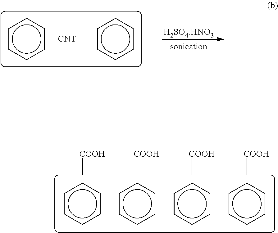
(6) Separately, one or more CNTs are sonicated in a mixture of nitric acid and sulfuric acid at a suitable ratio (e.g., 1:3) at a frequency, power and duration sufficient to functionalize the one or more CNTs with a carboxylic group to produce one or more carboxylic CNTs:
Figure US08563319-20131022-C00005
(7) The one or more carboxylic CNTs are mixed with tionyl chloride (SOCl2) in an amount sufficient to convert the carboxylic acid moieties to carboxylic chloride moieties to produce one or more COCl-CNTs:
Figure US08563319-20131022-C00006
(8) The one or more CNT-COCls (b) are reacted with the one or more Si substrates (a) having rinsed and dried NH2 terminated silicon surfaces (from Step #5) to produce one or more Si substrates coated or functionalized with one or more CNT moieties for NO2 detection:
Figure US08563319-20131022-C00007

No further processing is performed on the substrates to be used as sensing beams.
(9) For CNT-coated Si substrates intended for use as reference beams, however, selective direct printing of a monolayer of polyethylene on top of each of the one or more CNT-coated substrates is performed, thereby eliminating the ability of the reference beam to sense NO2.
Figure US08563319-20131022-C00008

Route #2
In this embodiment, a silicon substrate is functionalized with a CNT moiety by an alternate method. The process proceeds as outlined in Steps 1 and 2 above. Thereafter:
(3) The one or more H-terminated Si substrates are combined with a suitable amount of an allyl iodide and heated in a non-polar solvent, such as toluene, at a ratio and for a time and at a temperature sufficient to produce one or more iodine terminated (functionalized) Si substrates.
Figure US08563319-20131022-C00009
In one embodiment, the one or more H-terminated Si substrates are heated at a temperature of at least about 100° C., such as at least about 140 up to about 160° C., such as about 148 to about 152° C., or any range there between, for at least about two (2) (hr) up to six (6) hrs, such as about 3.5 to about 4.5 hrs, or any range there between, further including about four (4) hrs.
(4) The one or more iodine terminated (functionalized) Si substrates are cooled in ambient conditions down to room temperature.
(5) The one or more iodine terminated (functionalized) Si substrates are rinsed with a suitable unsaturated alcohol, such as ethanol and deionized water dried under nitrogen stream=to produce one or more processed Si substrates, with each of the one or more processed Si substrates having a rinsed and dried iodine-terminated silicon surface:
Figure US08563319-20131022-C00010
(6) Separately (as in Step (6) of Route #1 above), one or more CNTs are sonicated in a mixture of nitric acid and sulfuric acid at a suitable ratio (e.g., 1:3) at a frequency, power and duration sufficient to functionalize the one or more CNTs with a carboxylic group to produce one or more carboxylic CNTs:
Figure US08563319-20131022-C00011
7) The one or more carboxylic CNTs are sonicated in a suitable amount of sodium hydroxide (NaOH) at a frequency, power and duration sufficient to form one or more sodium salt CNTs:
Figure US08563319-20131022-C00012
8) The one or more sodium salt CNT's (b) are reacted with the one or more Si substrates (a), each having rinsed and dried iodine-terminated silicon surfaces (from Step #5) in the presence of a sufficient amount of a phase transfer catalyst (e.g., tetramethylammonium iodide) at a temperature in the range of 40-60° C. sufficient to produce one or more Si substrates coated or functionalized with one or more CNT moieties for NO2 detection:
Figure US08563319-20131022-C00013
No further processing is performed on the substrates to be used as sensing beams.
(9) For CNT-coated Si substrates intended for use as reference beams, selective direct printing of a monolayer of polyethylene on top of each of the one or more CNT-coated substrates is performed.
Route #3
In this embodiment, a silicon substrate is functionalized with a CNT moiety by an alternate method. The process proceeds as outlined in Steps 1 and 2 above. Thereafter:
(3) The one or more H-terminated Si substrates are combined with an allyl alcohol protected with benzyl groups in a suitable non-polar solvent, such as toluene, under conditions sufficient to produce one or more OH-terminated silicon substrates:
Figure US08563319-20131022-C00014
In one embodiment, the one or more H-terminated Si substrates are heated to a temperature of 100° C., such as at least about 140 up to about 160° C., such as about 148 to about 152° C., or any range there between, for at least about two (2) (hr) up to six (6) hrs, such as about 3.5 to about 4.5 hrs, or any range there between, further including about four (4) hrs.
(4) The one or more functionalized Si substrates are cooled under ambient conditions down to room temperature.
(5) The one or more cooled functionalized Si substrates are rinsed with an alcohol, such as ethanol and deionized water dried under nitrogen stream to produce one or more processed Si substrates:
(6) Deprotection of the alcohol is accomplished through hydrogenation according to the same reactions shown in Step 3 to produce one or more processed Si substrates:
(7) Separately (as in Step (6) of Route #1 above), one or more CNTs are sonicated in a mixture of nitric acid and sulfuric acid at a suitable ratio (e.g., 1:3) at a frequency, power and duration sufficient to functionalize the one or more CNTs with a carboxylic group to produce one or more carboxylic CNTs:
Figure US08563319-20131022-C00015
(8) The one or more carboxylic CNTs (b) are reacted with the one or more Si substrates (a) having rinsed and dried functionalized silicon surfaces (from Step #6) in the presence of a dicyclohexyl carbodiimide (DCC) in DMSO, at a temperature, such as 40-60° C., sufficient to produce one or more Si substrates coated or functionalized with one or more CNT moieties for NO2 detection. No further processing is performed on the substrates to be used as sensing beams:
Figure US08563319-20131022-C00016
(9) For CNT-coated Si substrates intended for use as reference beams, selective direct printing of a monolayer of polyethylene on top of each of the one or more CNT-coated substrates is performed.
Route #4
In this embodiment, a silicon substrate is functionalized with a CNT moiety by yet another alternate method. The process proceeds as outlined in Steps 1 and 2 above. Thereafter:
(3) The one or more H-terminated Si substrates are combined with an allyl iodide and potassium in a high-speed vibration mill under conditions sufficient to produce one or more H-terminated Si substrates.
Figure US08563319-20131022-C00017
(4) In one embodiment, the one or more H-terminated Si substrates synthesized in step 3 are heated in a non-polar solvent, such as toluene under conditions sufficient to produce one or more functionalized silicon substrates.
Figure US08563319-20131022-C00018
In one embodiment, the mixture is heated to a temperature of a 100° C., such as at least about 140 up to about 160° C., such as about 148 to about 152° C., or any range there between, for at least about two (2) (hr) up to six (6) hrs, such as about 3.5 to about 4.5 hrs, or any range there between, further including about four (4) hrs.
(5) The one or more functionalized Si substrates are cooled in ambient conditions down to room temperature.
(6) The one or more functionalized Si substrates are rinsed with an alcohol, such as ethanol and deionized water dried under nitrogen stream-to produce one or more dried processed Si substrates.
For functionalized Si substrates intended for use as reference beams, selective direct printing of a monolayer of polyethylene on top of each of the one or more CNT-coated substrates is performed.
Route #5
In this embodiment, a silicon substrate is functionalized with a ferrocene moiety. The process proceeds as outlined in Steps 1 and 2 above. for getting a hydrogen terminated silicon surface Thereafter:
(3) In one embodiment, the one or more H-terminated Si substrates synthesized in step 2 are combined with vinyl ferrocene together with a non-polar solvent, such as toluene, under conditions sufficient to produce one or more functionalized silicon substrates.
Figure US08563319-20131022-C00019
In one embodiment, the mixture is heated to a temperature of a 100° C., such as at least about 140 up to about 160° C., such as about 148 to about 152° C., or any range there between, for at least about two (2) (hr) up to six (6) hrs, such as about 3.5 to about 4.5 hrs, or any range there between, further including about four (4) hrs.
(5) The one or more functionalized Si substrates are cooled in ambient conditions down to room temperature.
(6) The one or more functionalized Si substrates are rinsed with an alcohol, such as ethanol and deionized water and dried undernitrogen stream to produce one or more dried and processed Si substrates.
For functionalized Si substrates intended for use as reference beams, selective direct printing of a monolayer of polyethylene on top of each of the one or more ferrocene-containing Si substrates is performed.
CONCLUSION
A novel a low cost, high performance NO2 gas sensor is provided which uses resonant differential principles. In one embodiment, this technology is applied to silicon nano-electromechanical systems (NEMS). In one embodiment, a vibrating functionalized nano-beam changes resonance frequency as a function of NO2 gas concentration in the ambient air.
Although specific embodiments have been illustrated and described herein, it will be appreciated by those of ordinary skill in the art that any procedure that is calculated to achieve the same purpose may be substituted for the specific embodiments shown. This application is intended to cover any adaptations or variations of the present subject matter. Therefore, it is manifestly intended that embodiments of this invention be limited only by the claims and the equivalents thereof.
The Abstract is provided to comply with 37 C.F.R. §1.72(b) is submitted with the understanding that it will not be used to interpret or limit the scope or meaning of the claims.

Claims (22)

What is claimed is:
1. A nitrogen dioxide sensor comprising:
a first beam having a first functionalized sensing surface capable of sensing nitrogen dioxide, the first beam capable of producing a first resonant frequency; and
a second beam having a second functionalized reference surface not capable of sensing nitrogen dioxide, the second beam capable of producing a second resonant frequency, wherein differential sensing of nitrogen dioxide may be performed, further wherein the first beam and the second beam are each functionalized with one or more soft bases having comparable viscoelastic properties.
2. The sensor of claim 1 wherein the second functionalized reference surface is altered with a polyethylene coating to prevent detection of nitrogen dioxide.
3. The sensor of claim 2 comprising a nano sensor capable of performing differential sensing by monitoring changes in the resonant frequency of the first beam relative to the resonant frequency of the second beam.
4. The sensor of claim 3 wherein the first beam and the second beam are located on a single silicon substrate.
5. The sensor of claim 3 wherein the first beam and the second beam are located on different silicon substrates.
6. The sensor of claim 1 wherein the one or more soft bases are selected from a conjugated aromatic hydrocarbon, a carbon nanotube, and a ferrocene moiety.
7. The sensor of claim 6 wherein the functionalized surface of the first beam contains carbon nanotube moieties as sensitive groups for nitrogen dioxide detection bonded downward to C═O and linked to the functionalized surface by carbon atoms and the functionalized surface of the second beam further contains a coating of polyethylene to prevent detection of nitrogen dioxide.
8. The sensor of claim 6 wherein the functionalized surface of the first beam contains ferrocene moieties as sensitive groups for nitrogen dioxide detection, and the functionalized surface of the second beam further contains a coating of polyethylene to prevent detection of nitrogen dioxide.
9. The sensor of claim 8, further comprising:
a first frequency measuring circuit for measuring the resonant frequency of the first beam;
a second frequency measuring circuit for measuring the resonant frequency of the second beam: and
a control for analyzing the signals from the first frequency measuring circuit and the second frequency measuring circuit, wherein a differential frequency equivalent to the first frequency minus the second frequency is determinable, wherein differential sensing of nitrogen dioxide exposure is performed.
10. The sensor of claim 6 comprising a low drift sensor capable of detecting nitrogen dioxide levels up to a zeptogram level.
11. The sensor of claim 1 wherein the first beam is functionalized with a first soft base and the second beam is functionalized with a second soft base.
12. A method comprising:
functionalizing a silicon surface with a first soft base to detect nitrogen dioxide; and
altering a portion of the functionalized silicon surface with a second soft base to prevent detection of nitrogen dioxide, wherein the second soft base has viscoelastic properties comparable to the first soft base.
13. The method of claim 12 wherein the silicon surface is functionalized with carbon nanotube moieties by first preparing an amino-terminated silicon surface or an iodine-terminated silicon surface.
14. The method of claim 12 wherein the silicon surface is functionalized through reaction of carboxylic carbon nanotubes with an alcohol-terminated silicon surface n the presence of dicyclohexil carbodiimide in DMSO.
15. The method of claim 12 wherein the silicon surface is functionalized through reaction of a compound synthesized by reacting carbon nanotubes with allyl iodide and potassium and hydrogen terminated silicon surfaces.
16. The method of claim 12 wherein the altering step comprises direct printing of a polyethylene coating on the portion of the functionalized silicon surface.
17. The method of claim 16 further comprising:
connecting frequency measuring devices to the silicon surface to produce differential resonant frequency changes;
connecting a mixer to the frequency measuring devices to measure the differential resonant frequency changes; and
outputting the differential resonant frequency changes to a presentation device.
18. The method of claim 12 wherein the silicon surface is a silicon wafer.
19. A method of detecting nitrogen dioxide comprising:
exposing first and second beams the silicon surface to nitrogen dioxide, wherein the first beam has a functionalized surface to detect nitrogen dioxide and the second beam has a functionalized surface altered to prevent detection of nitrogen dioxide; and
comparing the resonant frequency of the first beam silicon surface functionalized with a first soft base to the resonant frequency of second beam the portion of the functionalized silicon surface altered with the second soft base, wherein an amount of carbon nitrogen dioxide exposure is determined.
20. The method of claim 19 wherein the first and second beams functionalized silicon surfaces are nano-beams and the second beam second soft base is altered with a polyethylene coating.
21. The method of claim 20 wherein the first and second soft bases each comprise one or more soft bases.
22. The method of claim 21 wherein the one or more soft bases are selected from a conjugated aromatic hydrocarbon, a carbon nanotube, a ferrocene moiety, and combinations thereof.
US12/962,067 2009-12-11 2010-12-07 Differential resonators for NO2 detection and methods related thereto Expired - Fee Related US8563319B2 (en)

Applications Claiming Priority (3)

Application Number Priority Date Filing Date Title
EP09178792A EP2333531A1 (en) 2009-12-11 2009-12-11 Differential resonators for NO2 detection and methods related thereto
EP09178792.9 2009-12-11
EP09178792 2009-12-11

Publications (2)

Publication Number Publication Date
US20110143447A1 US20110143447A1 (en) 2011-06-16
US8563319B2 true US8563319B2 (en) 2013-10-22

Family

ID=42136029

Family Applications (1)

Application Number Title Priority Date Filing Date
US12/962,067 Expired - Fee Related US8563319B2 (en) 2009-12-11 2010-12-07 Differential resonators for NO2 detection and methods related thereto

Country Status (2)

Country Link
US (1) US8563319B2 (en)
EP (1) EP2333531A1 (en)

Cited By (1)

* Cited by examiner, † Cited by third party
Publication number Priority date Publication date Assignee Title
WO2019161319A1 (en) * 2018-02-17 2019-08-22 Northeast Gas Association Methane gas sensor

Families Citing this family (4)

* Cited by examiner, † Cited by third party
Publication number Priority date Publication date Assignee Title
EP2333532A1 (en) * 2009-12-11 2011-06-15 Honeywell Romania SRL Carbon dioxide sensor with functionalized resonating beams
CN104569076A (en) * 2015-01-08 2015-04-29 上海师范大学 Pencil drawing type NO2 sensing element and production method thereof
US11031167B2 (en) * 2017-11-21 2021-06-08 University Of New Hampshire Giant perpendicular magnetic anisotropy in Fe/GaN thin films for data storage and memory devices
CN109142452B (en) * 2018-10-26 2021-03-26 浙江师范大学 Blood viscoelastic force measuring device and method based on piezoresistive micro-suspension bridge sensor

Citations (31)

* Cited by examiner, † Cited by third party
Publication number Priority date Publication date Assignee Title
EP0072744A2 (en) 1981-08-17 1983-02-23 Allied Corporation Chemical sensor
US5552274A (en) * 1992-09-07 1996-09-03 Terumo Kabushiki Kaisha Method for detecting target sequences by oscillation frequency
US5932953A (en) * 1997-06-30 1999-08-03 Iowa State University Research Foundation, Inc. Method and system for detecting material using piezoelectric resonators
US6355498B1 (en) * 2000-08-11 2002-03-12 Agere Systems Guartian Corp. Thin film resonators fabricated on membranes created by front side releasing
US20030215865A1 (en) * 2002-04-26 2003-11-20 The Penn State Research Foundation Integrated nanomechanical sensor array chips
US20040093947A1 (en) * 2001-03-19 2004-05-20 Ralf Brederlow Micromechanic sensor element, electric circuit and sensor array comprising a plurality of micromechanic sensor elements
US20040150296A1 (en) * 2003-01-24 2004-08-05 Lg Electronics Inc. Material sensing sensor and module using thin film bulk acoustic resonator
US6866819B1 (en) * 2001-11-13 2005-03-15 Raytheon Company Sensor for detecting small concentrations of a target matter
US20060196253A1 (en) * 2002-08-29 2006-09-07 Bioscale, Inc. Resonant sensor and sensing system
US20060257286A1 (en) * 2003-10-17 2006-11-16 Adams Jesse D Self-sensing array of microcantilevers for chemical detection
US7280078B2 (en) * 2004-11-20 2007-10-09 Scenterra, Inc. Sensor for detecting high frequency signals
US7340941B1 (en) * 2002-10-01 2008-03-11 Xsilogy, Inc. Dense thin film-based chemical sensors and methods for making and using same
US20080110247A1 (en) 2006-06-02 2008-05-15 Board Of Trustees Of Michigan State University Sensor with microelectro-mechanical oscillators
US20080116490A1 (en) * 2006-10-19 2008-05-22 Stewart Duncan R Sensing method and nanosensing device for performing the same
WO2008088780A1 (en) 2007-01-12 2008-07-24 University Of Pittsburgh-Of The Commonwealth System Of Higher Education Detection of nitric oxide by nanostructured sensor
US7409851B2 (en) * 2005-03-29 2008-08-12 Cornell Research Foundation, Inc. Detection of small bound mass
US20100000292A1 (en) * 2008-07-02 2010-01-07 Stichting Imec Nederland Sensing device
US20100055801A1 (en) * 2008-08-26 2010-03-04 Dechang Yi Sensor for detecting and differentiating chemical analytes
US7694346B2 (en) * 2004-10-01 2010-04-06 Board Of Regents Of The Nevada System Of Higher Education On Behalf Of The University Of Nevada Cantilevered probe detector with piezoelectric element
US7691583B2 (en) * 2000-07-12 2010-04-06 Cornell Research Foundation, Inc. High sensitivity mechanical resonant sensor
US20100129920A1 (en) * 2005-12-15 2010-05-27 Imec Method and system for measuring physical parameters with a piezoelectric bimorph cantilever in a gaseous or liquid environment
US7770449B2 (en) * 2006-10-18 2010-08-10 Industrial Technology Research Institute Resistive-type humidity sensing structure with microbridge and method therefor
US7871569B2 (en) * 2003-12-30 2011-01-18 Intel Corporation Biosensor utilizing a resonator having a functionalized surface
US7892759B2 (en) * 2007-02-16 2011-02-22 Drexel University Enhanced sensitivity of a cantilever sensor via specific bindings
US7935191B2 (en) * 2006-08-09 2011-05-03 Drexel University Controlling accumulation of select adsorbers on a piezoelectric cantilever sensor
US20110113856A1 (en) 2009-11-13 2011-05-19 Honeywell International All-differential resonant nanosensor apparatus and method
US20110116974A1 (en) * 2009-11-19 2011-05-19 Honeywell Romania Srl Functionalized monolayers for carbon dioxide detection by a resonant nanosensor
US7959873B1 (en) * 2005-07-21 2011-06-14 California Institute Of Technology Biological detection based on differentially coupled nanomechanical systems using self-sensing cantilevers with attonewton force resolution
US20110143448A1 (en) * 2009-12-11 2011-06-16 Honeywell Romania S.R.L. So2 detection using differential nano-resonators and methods related thereto
US20120094270A1 (en) * 2006-01-23 2012-04-19 Rajakkannu Mutharasan Self-exciting, self-sensing piezoelectric cantilever sensor for detection of airborne analytes directly in air
US8168120B1 (en) * 2007-03-06 2012-05-01 The Research Foundation Of State University Of New York Reliable switch that is triggered by the detection of a specific gas or substance

Family Cites Families (1)

* Cited by examiner, † Cited by third party
Publication number Priority date Publication date Assignee Title
US20030024007A1 (en) 1998-12-02 2003-01-30 Cahoon Rebecca E. Plant Myb transcription factor homologs

Patent Citations (37)

* Cited by examiner, † Cited by third party
Publication number Priority date Publication date Assignee Title
EP0072744A2 (en) 1981-08-17 1983-02-23 Allied Corporation Chemical sensor
US5552274A (en) * 1992-09-07 1996-09-03 Terumo Kabushiki Kaisha Method for detecting target sequences by oscillation frequency
US5932953A (en) * 1997-06-30 1999-08-03 Iowa State University Research Foundation, Inc. Method and system for detecting material using piezoelectric resonators
US7691583B2 (en) * 2000-07-12 2010-04-06 Cornell Research Foundation, Inc. High sensitivity mechanical resonant sensor
US6355498B1 (en) * 2000-08-11 2002-03-12 Agere Systems Guartian Corp. Thin film resonators fabricated on membranes created by front side releasing
US20040093947A1 (en) * 2001-03-19 2004-05-20 Ralf Brederlow Micromechanic sensor element, electric circuit and sensor array comprising a plurality of micromechanic sensor elements
US6866819B1 (en) * 2001-11-13 2005-03-15 Raytheon Company Sensor for detecting small concentrations of a target matter
US20030215865A1 (en) * 2002-04-26 2003-11-20 The Penn State Research Foundation Integrated nanomechanical sensor array chips
US20060196253A1 (en) * 2002-08-29 2006-09-07 Bioscale, Inc. Resonant sensor and sensing system
US7340941B1 (en) * 2002-10-01 2008-03-11 Xsilogy, Inc. Dense thin film-based chemical sensors and methods for making and using same
US20040150296A1 (en) * 2003-01-24 2004-08-05 Lg Electronics Inc. Material sensing sensor and module using thin film bulk acoustic resonator
US20060257286A1 (en) * 2003-10-17 2006-11-16 Adams Jesse D Self-sensing array of microcantilevers for chemical detection
US7914740B2 (en) * 2003-12-30 2011-03-29 Intel Corporation Biosensor utilizing a resonator having a functionalized surface
US7871569B2 (en) * 2003-12-30 2011-01-18 Intel Corporation Biosensor utilizing a resonator having a functionalized surface
US7694346B2 (en) * 2004-10-01 2010-04-06 Board Of Regents Of The Nevada System Of Higher Education On Behalf Of The University Of Nevada Cantilevered probe detector with piezoelectric element
US8220067B2 (en) * 2004-10-01 2012-07-10 Board Of Regents Of The Nevada System Of Higher Education Cantilevered probe detector with piezoelectric element
US7280078B2 (en) * 2004-11-20 2007-10-09 Scenterra, Inc. Sensor for detecting high frequency signals
US7409851B2 (en) * 2005-03-29 2008-08-12 Cornell Research Foundation, Inc. Detection of small bound mass
US7959873B1 (en) * 2005-07-21 2011-06-14 California Institute Of Technology Biological detection based on differentially coupled nanomechanical systems using self-sensing cantilevers with attonewton force resolution
US20100129920A1 (en) * 2005-12-15 2010-05-27 Imec Method and system for measuring physical parameters with a piezoelectric bimorph cantilever in a gaseous or liquid environment
US20120094270A1 (en) * 2006-01-23 2012-04-19 Rajakkannu Mutharasan Self-exciting, self-sensing piezoelectric cantilever sensor for detection of airborne analytes directly in air
US20080110247A1 (en) 2006-06-02 2008-05-15 Board Of Trustees Of Michigan State University Sensor with microelectro-mechanical oscillators
US7935191B2 (en) * 2006-08-09 2011-05-03 Drexel University Controlling accumulation of select adsorbers on a piezoelectric cantilever sensor
US7770449B2 (en) * 2006-10-18 2010-08-10 Industrial Technology Research Institute Resistive-type humidity sensing structure with microbridge and method therefor
US20080116490A1 (en) * 2006-10-19 2008-05-22 Stewart Duncan R Sensing method and nanosensing device for performing the same
US20100282245A1 (en) * 2007-01-12 2010-11-11 Alexander Star Detection of nitric oxide
WO2008088780A1 (en) 2007-01-12 2008-07-24 University Of Pittsburgh-Of The Commonwealth System Of Higher Education Detection of nitric oxide by nanostructured sensor
US7892759B2 (en) * 2007-02-16 2011-02-22 Drexel University Enhanced sensitivity of a cantilever sensor via specific bindings
US8168120B1 (en) * 2007-03-06 2012-05-01 The Research Foundation Of State University Of New York Reliable switch that is triggered by the detection of a specific gas or substance
US20100000292A1 (en) * 2008-07-02 2010-01-07 Stichting Imec Nederland Sensing device
US8291745B2 (en) * 2008-07-02 2012-10-23 Stichting Imec Nederland Analyte sensing device
US20100055801A1 (en) * 2008-08-26 2010-03-04 Dechang Yi Sensor for detecting and differentiating chemical analytes
US7972865B2 (en) * 2008-08-26 2011-07-05 Ut-Battelle, Llc Sensor for detecting and differentiating chemical analytes
US20110113856A1 (en) 2009-11-13 2011-05-19 Honeywell International All-differential resonant nanosensor apparatus and method
US20110116974A1 (en) * 2009-11-19 2011-05-19 Honeywell Romania Srl Functionalized monolayers for carbon dioxide detection by a resonant nanosensor
US8230720B2 (en) * 2009-11-19 2012-07-31 Honeywell International Inc. Functionalized monolayers for carbon dioxide detection by a resonant nanosensor
US20110143448A1 (en) * 2009-12-11 2011-06-16 Honeywell Romania S.R.L. So2 detection using differential nano-resonators and methods related thereto

Non-Patent Citations (3)

* Cited by examiner, † Cited by third party
Title
Cobianu, C., et al., "All-Differential Resonant Nanosensor Apparatus and Method", U.S. Appl. No. 12/617,893, filed Nov. 13, 2009, 23 pgs.
Cobianu, C., et al., "Nano-scale resonant sensors for gas and bio detection: Expectations and challenges", International Semiconductor Conference, 2009. CAS 2009., XP031568982 ISBN : 978-1-4244-441,3-7, (2009), 259-262.
Durand, C, et al., "In-Plane Silicon-On-Nothing Nanometer-Scale Resonant Suspended Gate MOSFET for In-IC Integration Perspectives", IEEE Electron Device Letters, 29(5), XP0L1207042 ISSN: 0741-3106, (2008), 494-496.

Cited By (2)

* Cited by examiner, † Cited by third party
Publication number Priority date Publication date Assignee Title
WO2019161319A1 (en) * 2018-02-17 2019-08-22 Northeast Gas Association Methane gas sensor
US10627368B2 (en) 2018-02-17 2020-04-21 Applied Nanotech, Inc. Methane gas sensor

Also Published As

Publication number Publication date
US20110143447A1 (en) 2011-06-16
EP2333531A1 (en) 2011-06-15

Similar Documents

Publication Publication Date Title
US8563319B2 (en) Differential resonators for NO2 detection and methods related thereto
Su et al. Microcantilever resonance-based DNA detection with nanoparticle probes
Patil et al. An ultra-sensitive piezoresistive polymer nano-composite microcantilever sensor electronic nose platform for explosive vapor detection
Eom et al. Nanomechanical resonators and their applications in biological/chemical detection: Nanomechanics principles
Tamayo et al. Biosensors based on nanomechanical systems
Seena et al. Polymer nanocomposite nanomechanical cantilever sensors: material characterization, device development and application in explosive vapour detection
EP2327983B1 (en) Functionalized monolayers for carbon dioxide detection by a vibrating beam
US7814776B2 (en) Carbon nanotube-quartz resonator with femtogram resolution
Chen et al. Self-assembling siloxane bilayer directly on SiO2 surface of micro-cantilevers for long-term highly repeatable sensing to trace explosives
Tang et al. Fabrication and characterization of SiO2 microcantilever for microsensor application
JP2005537496A (en) Resonance sensor and sensing system
US9291600B2 (en) Piezoresistive NEMS array network
US20100215544A1 (en) Handheld microcantilever-based sensor for detecting tobacco-specific nitrosamines
US20110143448A1 (en) So2 detection using differential nano-resonators and methods related thereto
Koev et al. Mechano-transduction of DNA hybridization and dopamine oxidation through electrodeposited chitosan network
De Simoni et al. A surface-acoustic-wave-based cantilever bio-sensor
US8544314B2 (en) Carbon dioxide sensor with functionalized resonating beams
KR101045525B1 (en) How to introduce functional functional groups on the surface of the material
Serban et al. Differential resonators for NO2 detection and methods related thereto
Datskos et al. Chemical and biological sensors based on microcantilevers
Khanna Frontiers of nanosensor technology
Siwak et al. Indium phosphide MEMS cantilever resonator sensors utilizing a pentacene absorption layer
Lang Cantilever-based gas sensing
WO2010044394A1 (en) Alcohol concentration detecting element, alcohol concentration detector, and alcohol concentration detection method
Serban et al. Novel Concepts for CO2 detection by differential resonant nanosensing

Legal Events

Date Code Title Description
AS Assignment

Owner name: HONEYWELL ROMANIA S.R.L,, ROMANIA

Free format text: ASSIGNMENT OF ASSIGNORS INTEREST;ASSIGNORS:SERBAN, BOGDAN CATALIN;COBIANU, CORNEL P.;MIHAILA, MIHAI N.;AND OTHERS;SIGNING DATES FROM 20101112 TO 20101117;REEL/FRAME:025463/0191

STCF Information on status: patent grant

Free format text: PATENTED CASE

FPAY Fee payment

Year of fee payment: 4

FEPP Fee payment procedure

Free format text: MAINTENANCE FEE REMINDER MAILED (ORIGINAL EVENT CODE: REM.); ENTITY STATUS OF PATENT OWNER: LARGE ENTITY

LAPS Lapse for failure to pay maintenance fees

Free format text: PATENT EXPIRED FOR FAILURE TO PAY MAINTENANCE FEES (ORIGINAL EVENT CODE: EXP.); ENTITY STATUS OF PATENT OWNER: LARGE ENTITY

STCH Information on status: patent discontinuation

Free format text: PATENT EXPIRED DUE TO NONPAYMENT OF MAINTENANCE FEES UNDER 37 CFR 1.362

FP Lapsed due to failure to pay maintenance fee

Effective date: 20211022