US8577489B2 - Diagnosing in-line critical dimension control adjustments using optical proximity correction verification - Google Patents
Diagnosing in-line critical dimension control adjustments using optical proximity correction verification Download PDFInfo
- Publication number
- US8577489B2 US8577489B2 US13/014,152 US201113014152A US8577489B2 US 8577489 B2 US8577489 B2 US 8577489B2 US 201113014152 A US201113014152 A US 201113014152A US 8577489 B2 US8577489 B2 US 8577489B2
- Authority
- US
- United States
- Prior art keywords
- chip
- component dimensions
- determining
- simulating
- simulation
- Prior art date
- Legal status (The legal status is an assumption and is not a legal conclusion. Google has not performed a legal analysis and makes no representation as to the accuracy of the status listed.)
- Expired - Fee Related, expires
Links
Images


Classifications
-
- G—PHYSICS
- G03—PHOTOGRAPHY; CINEMATOGRAPHY; ANALOGOUS TECHNIQUES USING WAVES OTHER THAN OPTICAL WAVES; ELECTROGRAPHY; HOLOGRAPHY
- G03F—PHOTOMECHANICAL PRODUCTION OF TEXTURED OR PATTERNED SURFACES, e.g. FOR PRINTING, FOR PROCESSING OF SEMICONDUCTOR DEVICES; MATERIALS THEREFOR; ORIGINALS THEREFOR; APPARATUS SPECIALLY ADAPTED THEREFOR
- G03F1/00—Originals for photomechanical production of textured or patterned surfaces, e.g., masks, photo-masks, reticles; Mask blanks or pellicles therefor; Containers specially adapted therefor; Preparation thereof
- G03F1/36—Masks having proximity correction features; Preparation thereof, e.g. optical proximity correction [OPC] design processes
-
- G—PHYSICS
- G03—PHOTOGRAPHY; CINEMATOGRAPHY; ANALOGOUS TECHNIQUES USING WAVES OTHER THAN OPTICAL WAVES; ELECTROGRAPHY; HOLOGRAPHY
- G03F—PHOTOMECHANICAL PRODUCTION OF TEXTURED OR PATTERNED SURFACES, e.g. FOR PRINTING, FOR PROCESSING OF SEMICONDUCTOR DEVICES; MATERIALS THEREFOR; ORIGINALS THEREFOR; APPARATUS SPECIALLY ADAPTED THEREFOR
- G03F1/00—Originals for photomechanical production of textured or patterned surfaces, e.g., masks, photo-masks, reticles; Mask blanks or pellicles therefor; Containers specially adapted therefor; Preparation thereof
- G03F1/68—Preparation processes not covered by groups G03F1/20 - G03F1/50
- G03F1/70—Adapting basic layout or design of masks to lithographic process requirements, e.g., second iteration correction of mask patterns for imaging
-
- G—PHYSICS
- G03—PHOTOGRAPHY; CINEMATOGRAPHY; ANALOGOUS TECHNIQUES USING WAVES OTHER THAN OPTICAL WAVES; ELECTROGRAPHY; HOLOGRAPHY
- G03F—PHOTOMECHANICAL PRODUCTION OF TEXTURED OR PATTERNED SURFACES, e.g. FOR PRINTING, FOR PROCESSING OF SEMICONDUCTOR DEVICES; MATERIALS THEREFOR; ORIGINALS THEREFOR; APPARATUS SPECIALLY ADAPTED THEREFOR
- G03F7/00—Photomechanical, e.g. photolithographic, production of textured or patterned surfaces, e.g. printing surfaces; Materials therefor, e.g. comprising photoresists; Apparatus specially adapted therefor
- G03F7/70—Microphotolithographic exposure; Apparatus therefor
- G03F7/70483—Information management; Active and passive control; Testing; Wafer monitoring, e.g. pattern monitoring
- G03F7/70491—Information management, e.g. software; Active and passive control, e.g. details of controlling exposure processes or exposure tool monitoring processes
- G03F7/705—Modelling or simulating from physical phenomena up to complete wafer processes or whole workflow in wafer productions
Definitions
- the subject matter disclosed herein relates to diagnosing in-line critical dimension control adjustments. More specifically, the subject matter disclosed herein relates to using optical proximity correction verification (OPCV) to account for in-line critical dimension control adjustments.
- OPCV optical proximity correction verification
- OPCV simulations are most accurate when lithographic in-line conditions are run at the same conditions as used during the processing of wafers for model building.
- a specific structure e.g., a control structure
- CD target critical dimension
- the in-line target CD (and thus, the exposure dose used) may drift over time due to, e.g., feedback from the test structure. Therefore, the pass/fail criteria may not accurately predict fails in-line.
- the first approach involves ignoring the dose differences between the in-line target CD and the OPCV simulations. This approach, however, may create inaccuracies in prediction of the lithography.
- the second approach involves continually updating the production code to reflect changes in the in-line dose from the time the model was built through the time of OPCV simulation. However, this approach can introduce error in the lithography, because the dose setting used may not reflect the true dose applied, due to issues such as dose calibration, reflectivity, thin film interference, etc.
- a method includes: locating a control structure in a data set representing one of a chip or a kerf; simulating component dimensions within a region proximate to the control structure; determining a difference between the simulated component dimensions within the region and target component dimensions within the region; determining whether the difference exceeds a predetermined tolerance threshold; adjusting a simulation condition in response to determining the difference exceeds the predetermined tolerance threshold; and repeating the simulating of the component dimensions within the region, the determining of the difference, and the determining of whether the difference exceeds the predetermined tolerance threshold in response to the adjusting of the simulation condition.
- a first aspect includes a computer-implemented method of diagnosing in-line critical dimension control adjustments in a lithographic process, the method comprising: locating a control structure in a data set representing one of a chip or a kerf; simulating component dimensions within a region proximate to the control structure; determining a difference between the simulated component dimensions within the region and target component dimensions within the region; determining whether the difference exceeds a predetermined tolerance threshold; adjusting a simulation condition in response to determining the difference exceeds the predetermined tolerance threshold; and repeating the simulating of the component dimensions within the region, the determining of the difference, and the determining of whether the difference exceeds the predetermined tolerance threshold in response to the adjusting of the simulation condition.
- a second aspect includes a computer system comprising: at least one computing device configured to diagnose in-line critical dimension control adjustments in a lithographic process by performing actions comprising: locating a control structure in a data set representing one of a chip or a kerf; simulating component dimensions within a region proximate to the control structure; determining a difference between the simulated component dimensions within the region and target component dimensions within the region; determining whether the difference exceeds a predetermined tolerance threshold; adjusting a simulation condition in response to determining the difference exceeds the predetermined tolerance threshold; and repeating the simulating of the component dimensions within the region, the determining of the difference, and the determining of whether the difference exceeds the predetermined tolerance threshold in response to the adjusting of the simulation condition.
- a third aspect includes a computer program comprising program code embodied in at least one computer-readable storage medium, which when executed, enables a computer system to diagnose in-line critical dimension control adjustments in a lithographic process, the method comprising: locating a control structure in a data set representing one of a chip or a kerf; simulating component dimensions within a region proximate to the control structure; determining a difference between the simulated component dimensions within the region and target component dimensions within the region; determining whether the difference exceeds a predetermined tolerance threshold; adjusting a simulation condition in response to determining the difference exceeds the predetermined tolerance threshold; and repeating the simulating of the component dimensions within the region, the determining of the difference, and the determining of whether the difference exceeds the predetermined tolerance threshold in response to the adjusting of the simulation condition.
- FIG. 1 shows a flow diagram depicting a method according to embodiments.
- FIGS. 2-4 show schematic views of user interfaces according to embodiments.
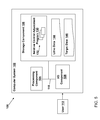
- FIG. 5 shows an illustrative environment for diagnosing in-line critical dimension control adjustments according to embodiments.
- embodiments disclosed relate to accounting for in-line critical dimension control adjustments using optical Proximity correction verification (OPCV). More specifically, embodiments disclosed relate to an iterative process including: simulating lithography of a control structure using initial process conditions (i.e., those starting process conditions which constitute the original centerpoint of model build data) to determine a simulated critical dimension at the control structure; comparing the simulated critical dimension with a target critical dimension chosen based upon how the production line desires to run the lithography process in question; and iteratively modifying lithography simulation conditions (e.g., dose, focus, etc.) to retarget the simulation of the critical dimension.
- initial process conditions i.e., those starting process conditions which constitute the original centerpoint of model build data
- a target critical dimension chosen based upon how the production line desires to run the lithography process in question
- iteratively modifying lithography simulation conditions e.g., dose, focus, etc.
- conventional OPCV methods may be used according to the modified conditions with the new centerpoint of
- a method including the following processes: a) locating a control structure in a data set representing one of a chip or a kerf; b) simulating component dimensions within a region proximate to the control structure; c) determining a difference between the simulated component dimensions within the region and target component dimensions within the region; d) determining whether the difference exceeds a predetermined tolerance threshold; e) adjusting a target lithography simulation condition in response to determining whether (and by how much) the difference exceeds the predetermined tolerance threshold; f) repeating the simulating of the component dimensions within the region, using the updated lithography conditions, and g) running full-chip OPCV using the lithography simulation condition iteratively defined in steps (e) and (f).
- data may be used interchangeably to refer to data representing the physical layout of one or more integrated circuit chips on a wafer.
- process P 1 A includes locating a control structure in chip data (e.g., chip layout data). That is, process P 1 A may include locating a process control structure for a wafer, which may include a plurality of integrated circuit chips and kerfs (separation regions) between those chips on the wafer.
- process P 1 B may be performed, where this process includes locating a control structure in a data set other than chip data.
- a control structure may be located in a kerf area (spacing between chips on the wafer), or in other chips from the same reticle (in the case where OPC verification is done on a chip-by-chip basis instead on a merged reticle data set).
- process P 2 using the control structure identified in either the chip data or e.g., the kerf data, component dimensions are simulated in a region proximate to the control structure. That is, process P 2 includes simulating the manufacture of components within a defined region around the control structure. For example, this may include simulating line ends, spacings, etc. in the region around the control structure (as well as the control structure itself). It is understood that in order to perform the simulation in process P 2 , target values representing target dimensions, spacings, etc. of the components within the region are obtained (in process P 1 C) from, e.g., a target data file or an in-line target control table, etc. as is known in the art.
- target values may be stored in, e.g., a data library, either after optical proximity correction (OPC), or by layer and technology type before OPC.
- OPC optical proximity correction
- initial (lithography) simulation conditions data object O 1
- These initial (lithography) simulation conditions may include exposure dose, focus, and other lithography conditions known in the art.
- iteration of process P 2 may involve modification of these initial lithography simulation conditions prior to re-simulation.
- process P 3 includes determining a difference (delta) between the simulated component dimensions and target component dimensions (as obtained in process P 1 C) within the defined region.
- the delta is compared to a predetermined tolerance (e.g. a tolerance band) to determine whether the target or the initial lithography simulation conditions require modification.
- a predetermined tolerance e.g. a tolerance band
- process P 4 A includes running optical proximity correction verification (OPCV) on the full-chip data.
- Running OPCV (or, optical rule checking, ORC) on the full-chip data according to the target lithography conditions (obtained in P 1 C) may be performed according to conventional methods known in the art. Accordingly, description of OPCV is omitted here for brevity. It is understood that in an optional embodiment, after running traditional OPCV on the full-chip data (process P 4 A), modification of the initial lithography simulation conditions (object O 1 ) for a subsequent chip simulation run may be performed in process PSB, according to known methods.
- the lithography simulation condition e.g., dose, focus, etc.
- the initial target value obtained in process P 1 C may be modified according to the adjusted simulation lithography conditions, and subsequently, simulation of component dimensions (process P 2 ) may be repeated with the modified simulation lithography conditions.
- FIGS. 2-4 show example structures and conditions illustrated according to embodiments disclosed herein. That is, FIGS. 2-4 are intended merely to illustrate some of the processes described herein, and should not be thought of as limiting the scope of those processes. Further, it is understood that FIGS. 2-4 may depict later-stage simulation processes after initial simulation and modification has occurred.
- FIG. 2 shows a user interface 12 illustrating a simulation 20 of a portion a static random access memory (SRAM) structure during an intermediate simulation process.
- This simulation 20 includes a design target dimension (e.g., a spacing between components) 22 , as presented in the original design data, and a simulated actual dimension 24 (simulated after OPC), which may deviate in some part from the design target dimension 22 .
- design target dimension 22 is equal to 130 nanometers (nm).
- simulated actual dimension 24 is measured at 130.5 nm.
- simulation controls 26 at this time in the simulation process are set to a dose level of 1.0.
- FIG. 3 shows the user interface 12 of FIG. 2 , including an additional simulation 30 of the static random access memory structure of FIG. 2 factoring in the manufacturing line target.
- adjustments made to the simulation conditions in these examples may be performed according to a predetermined adjustment criteria or assumptions based upon known targets.
- a predetermined adjustment criteria or assumptions based upon known targets. For example, in the illustrative example shown and described with reference to FIGS. 2-4 , it is understood that decreasing the dose (e.g., from 1.0 to 0.85, and subsequently, to 0.83) is known to bring the simulated actual dimensions closer to the original design target dimensions. Further, beyond knowing whether to increase or decrease the dose, it is understood that the amount of adjustment may be performed according to the predetermined adjustment criteria or assumptions based upon known targets.
- simulation 30 shows the manufacturing line target 32 , which is equal to 150 nm. That is, the width of the component is targeted to be 150 nm.
- manufacturing line target 32 will differ from the original design target ( 22 , FIG. 2 ) by 20 nanometers to accommodate for, e.g., process biases, such as the bias from lithography to reactive ion etching (RIE). Due to the differences between manufacturing line target 32 and original design target 22 ( FIG. 2 ), simulation may be performed again to account for these manufacturing line target differences.
- the result in this case, is a simulated actual dimension 34 , having a spacing of 147.5 nm.
- simulation controls 26 are set to a dose level of 0.85 in order to account for the manufacturing line target differences from the original design.
- the difference of 2.5 nm may be outside of the predetermined tolerance band (e.g., as described with reference to FIG. 1 ), and therefore, an adjustment to a lithography condition (e.g., dose) may help improve the simulation in this iterative process.
- FIG. 4 shows the user interface 12 of FIG. 3 , including an iterative simulation 40 of the simulation 30 of FIG. 3 . That is, FIG. 4 illustrates repeating the simulation of spacing (target 32 ) according to embodiments.
- simulation 40 shows that the second iteration produces a simulated actual dimension 44 of 150 nm, which is within the predetermined tolerance for manufacturing line target 32 (set at 150 nm).
- simulation controls 26 have been modified to a dose level of 0.83 in order to improve the simulation from the first iteration shown and described with reference to FIG. 3 . It is understood that once the simulation falls within the predetermined tolerance, full chip OPCV may be run (process P 4 A), which may identify other areas of a layout that aspects of the invention may improve.
- FIGS. 2-4 are merely illustrative of a simple iteration scenario at a particular simulation stage, and are in no way limiting of the teachings described herein. In some cases, several iterations or more may be necessary to improve the accuracy of the simulations described herein. It is further understood that while the dose is described as being modified in the examples of FIGS. 2-4 , focus and/or other lithographic conditions may be modified in order to improve the accuracy of simulations according to embodiments.
- FIG. 5 depicts an illustrative environment 100 for diagnosing in-line critical dimension control adjustments according to an embodiment.
- the environment 100 includes a computer system 102 that can perform a process described herein in order to generate a cut mask in an integrated circuit design.
- the computer system 102 is shown as including a lithography set point location program 130 , which makes computer system 102 operable to handle diagnosing in-line critical dimension control adjustments by performing any/all of the processes described herein and implementing any/all of the embodiments described herein.
- the computer system 102 is shown including a processing component 104 (e.g., one or more processors), a storage component 106 (e.g., a storage hierarchy), an input/output (I/O) component 108 (e.g., one or more I/O interfaces and/or devices), and a communications pathway 110 .
- the processing component 104 executes program code, such as the iterative control adjustment program 130 , which is at least partially fixed in the storage component 106 . While executing program code, the processing component 104 can process data, which can result in reading and/or writing transformed data from/to the storage component 106 and/or the I/O component 108 for further processing.
- the pathway 110 provides a communications link between each of the components in the computer system 102 .
- the I/O component 108 can comprise one or more human I/O devices, which enable a human user 112 to interact with the computer system 102 and/or one or more communications devices to enable a system user 112 to communicate with the computer system 102 using any type of communications link.
- the lithography set point location program 130 can manage a set of interfaces (e.g., graphical user interface(s), application program interface, etc.) that enable human and/or system users 112 to interact with the iterative control adjustment program 130 .
- the iterative control adjustment program 130 can manage (e.g., store, retrieve, create, manipulate, organize, present, etc.) data, such as lithography data 144 (e.g., initial litho conditions, object O 1 , FIG. 1 ), and/or target data 146 (e.g., target values obtained from target file(s) or target control table(s)), etc., using any solution.
- the computer system 102 can comprise one or more general purpose computing articles of manufacture (e.g., computing devices) capable of executing program code, such as the iterative control adjustment program 130 , installed thereon.
- program code means any collection of instructions, in any language, code or notation, that cause a computing device having an information processing capability to perform a particular function either directly or after any combination of the following: (a) conversion to another language, code or notation; (b) reproduction in a different material form; and/or (c) decompression.
- the lithography set point location program 130 can be embodied as any combination of system software and/or application software.
- the iterative control adjustment program 130 can be implemented using a set of modules 132 .
- a module 132 can enable the computer system 102 to perform a set of tasks used by the iterative control adjustment program 130 , and can be separately developed and/or implemented apart from other portions of the iterative control adjustment program 130 .
- the term “component” means any configuration of hardware, with or without software, which implements the functionality described in conjunction therewith using any solution, while the term “module” means program code that enables the computer system 102 to implement the functionality described in conjunction therewith using any solution.
- a module When fixed in a storage component 106 of a computer system 102 that includes a processing component 104 , a module is a substantial portion of a component that implements the functionality. Regardless, it is understood that two or more components, modules, and/or systems may share some/all of their respective hardware and/or software. Further, it is understood that some of the functionality discussed herein may not be implemented or additional functionality may be included as part of the computer system 102 .
- each computing device may have only a portion of iterative control adjustment program 130 fixed thereon (e.g., one or more modules 132 ).
- iterative control adjustment program 130 are only representative of various possible equivalent computer systems that may perform a process described herein.
- the functionality provided by the computer system 102 and iterative control adjustment program 130 can be at least partially implemented by one or more computing devices that include any combination of general and/or specific purpose hardware with or without program code.
- the hardware and program code, if included, can be created using standard engineering and programming techniques, respectively.
- the computing devices can communicate over any type of communications link. Further, while performing a process described herein, the computer system 102 can communicate with one or more other computer systems using any type of communications link. In either case, the communications link can comprise any combination of various types of wired and/or wireless links; comprise any combination of one or more types of networks; and/or utilize any combination of various types of transmission techniques and protocols.
- the computer system 102 can obtain or provide data, such as post-lithography data 144 (e.g., initial litho conditions, object O 1 , FIG. 1 ), and/or target data 146 (e.g., target values obtained from target file(s) or target control table(s)) using any solution.
- the computer system 102 can generate and/or be used to generate lithography data 144 and/or target data 146 , retrieve lithography data 144 and/or target data 146 , from one or more data stores, receive lithography data 144 and/or target data 146 , from another system, send lithography data 144 and/or target data 146 to another system, etc.
- the invention provides a computer program fixed in at least one computer-readable medium, which when executed, enables a computer system to diagnosing in-line critical dimension control adjustments.
- the computer-readable medium includes program code, such as the iterative control adjustment program 130 ( FIG. 5 ), which implements some or all of the processes and/or embodiments described herein.
- the term “computer-readable medium” comprises one or more of any type of tangible medium of expression, now known or later developed, from which a copy of the program code can be perceived, reproduced, or otherwise communicated by a computing device.
- the computer-readable medium can comprise: one or more portable storage articles of manufacture; one or more memory/storage components of a computing device; paper; etc.
- the invention provides a method of providing a copy of program code, such as the iterative control adjustment program 130 ( FIG. 5 ), which implements some or all of a process described herein.
- a computer system can process a copy of program code that implements some or all of a process described herein to generate and transmit, for reception at a second, distinct location, a set of data signals that has one or more of its characteristics set and/or changed in such a manner as to encode a copy of the program code in the set of data signals.
- an embodiment of the invention provides a method of acquiring a copy of program code that implements some or all of a process described herein, which includes a computer system receiving the set of data signals described herein, and translating the set of data signals into a copy of the computer program fixed in at least one computer-readable medium.
- the set of data signals can be transmitted/received using any type of communications link.
- the invention provides a method of generating a system for determining a lithographic set point.
- a computer system such as the computer system 102 ( FIG. 10 ) can be obtained (e.g., created, maintained, made available, etc.) and one or more components for performing a process described herein can be obtained (e.g., created, purchased, used, modified, etc.) and deployed to the computer system.
- the deployment can comprise one or more of: (1) installing program code on a computing device; (2) adding one or more computing and/or I/O devices to the computer system; (3) incorporating and/or modifying the computer system to enable it to perform a process described herein; etc.
Abstract
Description
Claims (19)
Priority Applications (1)
| Application Number | Priority Date | Filing Date | Title |
|---|---|---|---|
| US13/014,152 US8577489B2 (en) | 2011-01-26 | 2011-01-26 | Diagnosing in-line critical dimension control adjustments using optical proximity correction verification |
Applications Claiming Priority (1)
| Application Number | Priority Date | Filing Date | Title |
|---|---|---|---|
| US13/014,152 US8577489B2 (en) | 2011-01-26 | 2011-01-26 | Diagnosing in-line critical dimension control adjustments using optical proximity correction verification |
Publications (2)
| Publication Number | Publication Date |
|---|---|
| US20120191234A1 US20120191234A1 (en) | 2012-07-26 |
| US8577489B2 true US8577489B2 (en) | 2013-11-05 |
Family
ID=46544757
Family Applications (1)
| Application Number | Title | Priority Date | Filing Date |
|---|---|---|---|
| US13/014,152 Expired - Fee Related US8577489B2 (en) | 2011-01-26 | 2011-01-26 | Diagnosing in-line critical dimension control adjustments using optical proximity correction verification |
Country Status (1)
| Country | Link |
|---|---|
| US (1) | US8577489B2 (en) |
Families Citing this family (3)
| Publication number | Priority date | Publication date | Assignee | Title |
|---|---|---|---|---|
| US8619236B2 (en) | 2010-11-24 | 2013-12-31 | International Business Machines Corporation | Determining lithographic set point using optical proximity correction verification simulation |
| US8577489B2 (en) | 2011-01-26 | 2013-11-05 | International Business Machines Corporation | Diagnosing in-line critical dimension control adjustments using optical proximity correction verification |
| US8499260B2 (en) * | 2011-01-26 | 2013-07-30 | International Business Machines Corporation | Optical proximity correction verification accounting for mask deviations |
Citations (48)
| Publication number | Priority date | Publication date | Assignee | Title |
|---|---|---|---|---|
| US5800951A (en) | 1995-11-22 | 1998-09-01 | Nec Corporation | Exposure method and exposure mask with monitoring patterns |
| US6067375A (en) | 1995-03-13 | 2000-05-23 | Sony Corporation | Correction method and correction apparatus of mask pattern |
| US6106980A (en) | 1997-05-16 | 2000-08-22 | Micron Technology, Inc. | Method and apparatus to accurately correlate defect coordinates between photomask inspection and repair systems |
| US6187687B1 (en) * | 1998-11-05 | 2001-02-13 | Advanced Micro Devices, Inc. | Minimization of line width variation in photolithography |
| US6415421B2 (en) | 2000-06-13 | 2002-07-02 | Mentor Graphics Corporation | Integrated verification and manufacturability tool |
| US6425117B1 (en) * | 1995-03-06 | 2002-07-23 | Lsi Logic Corporation | System and method for performing optical proximity correction on the interface between optical proximity corrected cells |
| US6600551B2 (en) * | 1997-06-27 | 2003-07-29 | Pixelligent Technologies Llc | Programmable photolithographic mask system and method |
| US6606533B1 (en) | 2000-10-12 | 2003-08-12 | International Business Machines Corporation | Method and arrangement for controlling image size of integrated circuits on wafers through post-exposure bake hotplate-specific dose feedback |
| US20030219154A1 (en) | 2002-05-22 | 2003-11-27 | Medvedeva Marina M. | Quality measurement of an aerial image |
| US6665856B1 (en) | 2000-12-01 | 2003-12-16 | Numerical Technologies, Inc. | Displacing edge segments on a fabrication layout based on proximity effects model amplitudes for correcting proximity effects |
| US6766507B2 (en) | 2002-04-12 | 2004-07-20 | International Business Machines Corporation | Mask/wafer control structure and algorithm for placement |
| US20040268291A1 (en) | 2003-06-24 | 2004-12-30 | Micron Technology, Inc. | Method and device for checking lithography data |
| US20050055658A1 (en) | 2003-09-09 | 2005-03-10 | International Business Machines Corporation | Method for adaptive segment refinement in optical proximity correction |
| US6952818B2 (en) | 2001-11-26 | 2005-10-04 | Kabushiki Kaisha Toshiba | Method and system for optical proximity correction |
| US7065738B1 (en) | 2004-05-04 | 2006-06-20 | Advanced Micro Devices, Inc. | Method of verifying an optical proximity correction (OPC) model |
| US7093229B2 (en) | 1997-09-17 | 2006-08-15 | Synopsys, Inc. | System and method for providing defect printability analysis of photolithographic masks with job-based automation |
| US7114145B2 (en) | 2003-10-07 | 2006-09-26 | Brion Technologies, Inc. | System and method for lithography simulation |
| US20070031745A1 (en) | 2005-08-08 | 2007-02-08 | Brion Technologies, Inc. | System and method for creating a focus-exposure model of a lithography process |
| US20070113216A1 (en) | 2005-11-14 | 2007-05-17 | Youping Zhang | Photolithographic mask correction |
| US7233887B2 (en) | 2002-01-18 | 2007-06-19 | Smith Bruce W | Method of photomask correction and its optimization using localized frequency analysis |
| US7245356B2 (en) | 2003-02-11 | 2007-07-17 | Asml Netherlands B.V. | Lithographic apparatus and method for optimizing illumination using a photolithographic simulation |
| US7264906B2 (en) | 2004-03-05 | 2007-09-04 | Lsi Corporation | OPC based illumination optimization with mask error constraints |
| US7281222B1 (en) | 2004-06-02 | 2007-10-09 | Advanced Micro Devices, Inc. | System and method for automatic generation of optical proximity correction (OPC) rule sets |
| US20070292778A1 (en) * | 2006-06-15 | 2007-12-20 | Bang Kyoung-Yoon | Methods of measuring critical dimensions and related devices |
| US7318214B1 (en) | 2003-06-19 | 2008-01-08 | Invarium, Inc. | System and method for reducing patterning variability in integrated circuit manufacturing through mask layout corrections |
| US7325222B2 (en) | 2004-03-12 | 2008-01-29 | Lsi Logic Corporation | Method and apparatus for verifying the post-optical proximity corrected mask wafer image sensitivity to reticle manufacturing errors |
| US7350183B2 (en) * | 2004-11-05 | 2008-03-25 | International Business Machines Corporation | Method for improving optical proximity correction |
| US7383530B2 (en) | 2003-05-05 | 2008-06-03 | Taiwan Semiconductor Manufacturing Company, Ltd | System and method for examining mask pattern fidelity |
| US20080204690A1 (en) | 2006-11-08 | 2008-08-28 | Gabriel Berger | Method, program product and apparatus for generating a calibrated pupil kernel and method of using the same in a lithography simulation process |
| US7480890B2 (en) | 2005-08-09 | 2009-01-20 | Powerchip Semiconductor Corp. | Method for correcting and configuring optical mask pattern |
| US20090031262A1 (en) | 2007-07-26 | 2009-01-29 | Shimon Maeda | Mask pattern formation method, mask pattern formation apparatus, and lithography mask |
| US20090100389A1 (en) | 2007-10-11 | 2009-04-16 | Ir Kusnadi | Shape-based photolithographic model calibration |
| US20090132992A1 (en) | 2007-11-21 | 2009-05-21 | Chartered Semiconductor Manufacturing, Ltd. | Statistical optical proximity correction |
| US20090157360A1 (en) * | 2007-12-05 | 2009-06-18 | Jun Ye | Methods and system for lithography process window simulation |
| JP2009139632A (en) | 2007-12-06 | 2009-06-25 | Elpida Memory Inc | Mask pattern correction method and exposure mask |
| US7587704B2 (en) | 2005-09-09 | 2009-09-08 | Brion Technologies, Inc. | System and method for mask verification using an individual mask error model |
| US20090246975A1 (en) * | 2008-03-27 | 2009-10-01 | Taiwan Semiconductor Manufacturing Company, Ltd. | Multiple technology node mask |
| US7624369B2 (en) | 2006-10-31 | 2009-11-24 | International Business Machines Corporation | Closed-loop design for manufacturability process |
| US7646906B2 (en) | 2004-01-29 | 2010-01-12 | Kla-Tencor Technologies Corp. | Computer-implemented methods for detecting defects in reticle design data |
| US7689966B2 (en) | 2004-09-14 | 2010-03-30 | Kla-Tencor Technologies Corp. | Methods, systems, and carrier media for evaluating reticle layout data |
| US7694267B1 (en) | 2006-02-03 | 2010-04-06 | Brion Technologies, Inc. | Method for process window optimized optical proximity correction |
| US7695876B2 (en) | 2005-08-31 | 2010-04-13 | Brion Technologies, Inc. | Method for identifying and using process window signature patterns for lithography process control |
| US20100122225A1 (en) | 2008-11-10 | 2010-05-13 | Yu Cao | Pattern selection for lithographic model calibration |
| US20100162197A1 (en) | 2008-12-18 | 2010-06-24 | Brion Technologies Inc. | Method and system for lithography process-window-maximixing optical proximity correction |
| US7752595B2 (en) | 2006-08-28 | 2010-07-06 | Kabushiki Kaisha Toshiba | Method for verifying and correcting post-OPC pattern layout |
| US20100175042A1 (en) | 2009-01-06 | 2010-07-08 | International Business Machines Corporation | Efficient isotropic modeling approach to incorporate electromagnetic effects into lithographic process simulations |
| US8014991B2 (en) * | 2003-09-30 | 2011-09-06 | Tokyo Electron Limited | System and method for using first-principles simulation to characterize a semiconductor manufacturing process |
| US20120191234A1 (en) | 2011-01-26 | 2012-07-26 | International Business Machines Corporation | Diagnosing in-line critical dimension control adjustments using optical proximity correction verification |
-
2011
- 2011-01-26 US US13/014,152 patent/US8577489B2/en not_active Expired - Fee Related
Patent Citations (54)
| Publication number | Priority date | Publication date | Assignee | Title |
|---|---|---|---|---|
| US6425117B1 (en) * | 1995-03-06 | 2002-07-23 | Lsi Logic Corporation | System and method for performing optical proximity correction on the interface between optical proximity corrected cells |
| US6067375A (en) | 1995-03-13 | 2000-05-23 | Sony Corporation | Correction method and correction apparatus of mask pattern |
| US5800951A (en) | 1995-11-22 | 1998-09-01 | Nec Corporation | Exposure method and exposure mask with monitoring patterns |
| US6106980A (en) | 1997-05-16 | 2000-08-22 | Micron Technology, Inc. | Method and apparatus to accurately correlate defect coordinates between photomask inspection and repair systems |
| US6888616B2 (en) * | 1997-06-27 | 2005-05-03 | Pixelligent Technologies Llc | Programmable photolithographic mask system and method |
| US6600551B2 (en) * | 1997-06-27 | 2003-07-29 | Pixelligent Technologies Llc | Programmable photolithographic mask system and method |
| US7093229B2 (en) | 1997-09-17 | 2006-08-15 | Synopsys, Inc. | System and method for providing defect printability analysis of photolithographic masks with job-based automation |
| US6187687B1 (en) * | 1998-11-05 | 2001-02-13 | Advanced Micro Devices, Inc. | Minimization of line width variation in photolithography |
| US6415421B2 (en) | 2000-06-13 | 2002-07-02 | Mentor Graphics Corporation | Integrated verification and manufacturability tool |
| US6606533B1 (en) | 2000-10-12 | 2003-08-12 | International Business Machines Corporation | Method and arrangement for controlling image size of integrated circuits on wafers through post-exposure bake hotplate-specific dose feedback |
| US6665856B1 (en) | 2000-12-01 | 2003-12-16 | Numerical Technologies, Inc. | Displacing edge segments on a fabrication layout based on proximity effects model amplitudes for correcting proximity effects |
| US6952818B2 (en) | 2001-11-26 | 2005-10-04 | Kabushiki Kaisha Toshiba | Method and system for optical proximity correction |
| US7233887B2 (en) | 2002-01-18 | 2007-06-19 | Smith Bruce W | Method of photomask correction and its optimization using localized frequency analysis |
| US6766507B2 (en) | 2002-04-12 | 2004-07-20 | International Business Machines Corporation | Mask/wafer control structure and algorithm for placement |
| US20030219154A1 (en) | 2002-05-22 | 2003-11-27 | Medvedeva Marina M. | Quality measurement of an aerial image |
| US7245356B2 (en) | 2003-02-11 | 2007-07-17 | Asml Netherlands B.V. | Lithographic apparatus and method for optimizing illumination using a photolithographic simulation |
| US7383530B2 (en) | 2003-05-05 | 2008-06-03 | Taiwan Semiconductor Manufacturing Company, Ltd | System and method for examining mask pattern fidelity |
| US7318214B1 (en) | 2003-06-19 | 2008-01-08 | Invarium, Inc. | System and method for reducing patterning variability in integrated circuit manufacturing through mask layout corrections |
| US20040268291A1 (en) | 2003-06-24 | 2004-12-30 | Micron Technology, Inc. | Method and device for checking lithography data |
| US20050055658A1 (en) | 2003-09-09 | 2005-03-10 | International Business Machines Corporation | Method for adaptive segment refinement in optical proximity correction |
| US8014991B2 (en) * | 2003-09-30 | 2011-09-06 | Tokyo Electron Limited | System and method for using first-principles simulation to characterize a semiconductor manufacturing process |
| US7114145B2 (en) | 2003-10-07 | 2006-09-26 | Brion Technologies, Inc. | System and method for lithography simulation |
| US7646906B2 (en) | 2004-01-29 | 2010-01-12 | Kla-Tencor Technologies Corp. | Computer-implemented methods for detecting defects in reticle design data |
| US7264906B2 (en) | 2004-03-05 | 2007-09-04 | Lsi Corporation | OPC based illumination optimization with mask error constraints |
| US7325222B2 (en) | 2004-03-12 | 2008-01-29 | Lsi Logic Corporation | Method and apparatus for verifying the post-optical proximity corrected mask wafer image sensitivity to reticle manufacturing errors |
| US7065738B1 (en) | 2004-05-04 | 2006-06-20 | Advanced Micro Devices, Inc. | Method of verifying an optical proximity correction (OPC) model |
| US7281222B1 (en) | 2004-06-02 | 2007-10-09 | Advanced Micro Devices, Inc. | System and method for automatic generation of optical proximity correction (OPC) rule sets |
| US7689966B2 (en) | 2004-09-14 | 2010-03-30 | Kla-Tencor Technologies Corp. | Methods, systems, and carrier media for evaluating reticle layout data |
| US7350183B2 (en) * | 2004-11-05 | 2008-03-25 | International Business Machines Corporation | Method for improving optical proximity correction |
| US20070031745A1 (en) | 2005-08-08 | 2007-02-08 | Brion Technologies, Inc. | System and method for creating a focus-exposure model of a lithography process |
| US7480890B2 (en) | 2005-08-09 | 2009-01-20 | Powerchip Semiconductor Corp. | Method for correcting and configuring optical mask pattern |
| US7695876B2 (en) | 2005-08-31 | 2010-04-13 | Brion Technologies, Inc. | Method for identifying and using process window signature patterns for lithography process control |
| US8057967B2 (en) | 2005-08-31 | 2011-11-15 | Asml Netherlands B.V. | Process window signature patterns for lithography process control |
| US7587704B2 (en) | 2005-09-09 | 2009-09-08 | Brion Technologies, Inc. | System and method for mask verification using an individual mask error model |
| US7617477B2 (en) | 2005-09-09 | 2009-11-10 | Brion Technologies, Inc. | Method for selecting and optimizing exposure tool using an individual mask error model |
| US20070113216A1 (en) | 2005-11-14 | 2007-05-17 | Youping Zhang | Photolithographic mask correction |
| US20100180251A1 (en) | 2006-02-03 | 2010-07-15 | Brion Technology, Inc. | Method for process window optimized optical proximity correction |
| US7694267B1 (en) | 2006-02-03 | 2010-04-06 | Brion Technologies, Inc. | Method for process window optimized optical proximity correction |
| US20070292778A1 (en) * | 2006-06-15 | 2007-12-20 | Bang Kyoung-Yoon | Methods of measuring critical dimensions and related devices |
| US7752595B2 (en) | 2006-08-28 | 2010-07-06 | Kabushiki Kaisha Toshiba | Method for verifying and correcting post-OPC pattern layout |
| US7624369B2 (en) | 2006-10-31 | 2009-11-24 | International Business Machines Corporation | Closed-loop design for manufacturability process |
| US20080204690A1 (en) | 2006-11-08 | 2008-08-28 | Gabriel Berger | Method, program product and apparatus for generating a calibrated pupil kernel and method of using the same in a lithography simulation process |
| US20090031262A1 (en) | 2007-07-26 | 2009-01-29 | Shimon Maeda | Mask pattern formation method, mask pattern formation apparatus, and lithography mask |
| US20090100389A1 (en) | 2007-10-11 | 2009-04-16 | Ir Kusnadi | Shape-based photolithographic model calibration |
| US7805699B2 (en) | 2007-10-11 | 2010-09-28 | Mentor Graphics Corporation | Shape-based photolithographic model calibration |
| US20090132992A1 (en) | 2007-11-21 | 2009-05-21 | Chartered Semiconductor Manufacturing, Ltd. | Statistical optical proximity correction |
| US20090157360A1 (en) * | 2007-12-05 | 2009-06-18 | Jun Ye | Methods and system for lithography process window simulation |
| US8200468B2 (en) * | 2007-12-05 | 2012-06-12 | Asml Netherlands B.V. | Methods and system for lithography process window simulation |
| JP2009139632A (en) | 2007-12-06 | 2009-06-25 | Elpida Memory Inc | Mask pattern correction method and exposure mask |
| US20090246975A1 (en) * | 2008-03-27 | 2009-10-01 | Taiwan Semiconductor Manufacturing Company, Ltd. | Multiple technology node mask |
| US20100122225A1 (en) | 2008-11-10 | 2010-05-13 | Yu Cao | Pattern selection for lithographic model calibration |
| US20100162197A1 (en) | 2008-12-18 | 2010-06-24 | Brion Technologies Inc. | Method and system for lithography process-window-maximixing optical proximity correction |
| US20100175042A1 (en) | 2009-01-06 | 2010-07-08 | International Business Machines Corporation | Efficient isotropic modeling approach to incorporate electromagnetic effects into lithographic process simulations |
| US20120191234A1 (en) | 2011-01-26 | 2012-07-26 | International Business Machines Corporation | Diagnosing in-line critical dimension control adjustments using optical proximity correction verification |
Non-Patent Citations (12)
| Title |
|---|
| Anderson et al., "Optimizing process window robustness with reconfigurable OPC (reconfigurable optical proximity correction)", Solid State Technology 2006. |
| Ban et al., "A Fast Lithography Verification Framework for Litho-Friendly Layout Design", Proceedings of the Sixth International Symposium on Quality Electronic Design, 2005. |
| Hung et al., "Post-OPC verification using a full-chip Pattern-Based simulation verification method", 25th Annual BACUS Symposium on Photomask Technology, 2005. |
| Jank et al., "Method for fast and accurate calibration of litho simulator for hot spot analysis", PE-82. |
| Lin: U.S. Appl. No. 13/014,159, filed Jan. 26, 2011, ExParteQuayle, Oct. 12, 2012, 14 pgs. |
| Lin: U.S. Appl. No. 13/014,159, filed Jan. 26, 2011, Notice of Allowance, Jan. 11, 2013, 5 pgs. |
| Lucas, et al., Patterning control budgets for the 32nm generation incorporating lithography, design, and RET variations, Optical Microlithography XX, Proc. of SPIE, vol. 6520, 65200N, 2007. |
| Riddle: U.S. Appl. No. 12/953,511, Office Action Mar. 1, 2013, 24pages. |
| Rodrigues, et al., "Optical Lithography Simulation with Focus Variation using Wavelet Transform", IEEE 2010. |
| Sturtevant et al., "Novel Method for Optimizing Lithography Exposure Conditions using Full-Chip Post-OPC Simulation", Optical Microlithography XXI, 2008. |
| Word et al., "Lithography yield enhancement through optical rule checking", Advanced Microlithography Technologies, 2005. |
| Zach et al., "Process dependencies of Optical Proximity Corrections", Optical Microlithography XIV, Proceedings of SPIE vol. 4346, 2001. |
Also Published As
| Publication number | Publication date |
|---|---|
| US20120191234A1 (en) | 2012-07-26 |
Similar Documents
| Publication | Publication Date | Title |
|---|---|---|
| US8103983B2 (en) | Electrically-driven optical proximity correction to compensate for non-optical effects | |
| US7624369B2 (en) | Closed-loop design for manufacturability process | |
| CN102841509B (en) | Integration of lithography apparatus and mask optimization process with multiple patterning process | |
| US8255838B2 (en) | Etch-aware OPC model calibration by using an etch bias filter | |
| US8331646B2 (en) | Optical proximity correction for transistors using harmonic mean of gate length | |
| JP2010506336A (en) | Characteristics in electronic design automation. | |
| TWI547753B (en) | Methods and systems for designing and manufacturing optical lithography masks | |
| US8997027B2 (en) | Methods for modifying an integrated circuit layout design | |
| US7260812B2 (en) | Method and apparatus for expediting convergence in model-based OPC | |
| US8887105B1 (en) | Calibration pattern selection based on noise sensitivity | |
| US8577489B2 (en) | Diagnosing in-line critical dimension control adjustments using optical proximity correction verification | |
| US8880382B2 (en) | Analyzing a patterning process using a model of yield | |
| US20190102501A1 (en) | Simulation-Assisted Wafer Rework Determination | |
| US9311442B2 (en) | Net-voltage-aware optical proximity correction (OPC) | |
| US9500945B1 (en) | Pattern classification based proximity corrections for reticle fabrication | |
| JP2006343217A (en) | Circuit simulation method and circuit simulation device | |
| US8166423B2 (en) | Photomask design verification | |
| US20120198394A1 (en) | Method For Improving Circuit Design Robustness | |
| US20220283511A1 (en) | Method and apparatus for controlling a computing process | |
| US9135391B2 (en) | Determination of electromigration susceptibility based on hydrostatic stress analysis | |
| US8499260B2 (en) | Optical proximity correction verification accounting for mask deviations | |
| US8881070B1 (en) | Optical proximity correction based on edge fragment correlation | |
| US8619236B2 (en) | Determining lithographic set point using optical proximity correction verification simulation | |
| CN113608410A (en) | Wafer alignment mask generation method and device, computer equipment and storage medium | |
| US8458632B2 (en) | Efficient slack projection for truncated distributions |
Legal Events
| Date | Code | Title | Description |
|---|---|---|---|
| AS | Assignment |
Owner name: INTERNATIONAL BUSINESS MACHINES CORPORATION, NEW Y Free format text: ASSIGNMENT OF ASSIGNORS INTEREST;ASSIGNORS:BRUCE, JAMES A;SETTLEMYER, KENNETH T, JR;SIGNING DATES FROM 20101210 TO 20101212;REEL/FRAME:025700/0649 |
|
| AS | Assignment |
Owner name: GLOBALFOUNDRIES U.S. 2 LLC, NEW YORK Free format text: ASSIGNMENT OF ASSIGNORS INTEREST;ASSIGNOR:INTERNATIONAL BUSINESS MACHINES CORPORATION;REEL/FRAME:036550/0001 Effective date: 20150629 |
|
| AS | Assignment |
Owner name: GLOBALFOUNDRIES INC., CAYMAN ISLANDS Free format text: ASSIGNMENT OF ASSIGNORS INTEREST;ASSIGNORS:GLOBALFOUNDRIES U.S. 2 LLC;GLOBALFOUNDRIES U.S. INC.;REEL/FRAME:036779/0001 Effective date: 20150910 |
|
| REMI | Maintenance fee reminder mailed | ||
| LAPS | Lapse for failure to pay maintenance fees |
Free format text: PATENT EXPIRED FOR FAILURE TO PAY MAINTENANCE FEES (ORIGINAL EVENT CODE: EXP.) |
|
| STCH | Information on status: patent discontinuation |
Free format text: PATENT EXPIRED DUE TO NONPAYMENT OF MAINTENANCE FEES UNDER 37 CFR 1.362 |
|
| FP | Lapsed due to failure to pay maintenance fee |
Effective date: 20171105 |
|
| AS | Assignment |
Owner name: GLOBALFOUNDRIES U.S. INC., NEW YORK Free format text: RELEASE BY SECURED PARTY;ASSIGNOR:WILMINGTON TRUST, NATIONAL ASSOCIATION;REEL/FRAME:056987/0001 Effective date: 20201117 |