US8586204B2 - Phosphorescent emitters and host materials with improved stability - Google Patents
Phosphorescent emitters and host materials with improved stability Download PDFInfo
- Publication number
- US8586204B2 US8586204B2 US12/869,284 US86928410A US8586204B2 US 8586204 B2 US8586204 B2 US 8586204B2 US 86928410 A US86928410 A US 86928410A US 8586204 B2 US8586204 B2 US 8586204B2
- Authority
- US
- United States
- Prior art keywords
- compound
- compounds
- mmol
- materials
- organic
- Prior art date
- Legal status (The legal status is an assumption and is not a legal conclusion. Google has not performed a legal analysis and makes no representation as to the accuracy of the status listed.)
- Active, expires
Links
- 0 *.B.C.CC.CC.CC.CC.[1*]CC(C[2*])N1=C(/C=C\C)N(C)=CC1 Chemical compound *.B.C.CC.CC.CC.CC.[1*]CC(C[2*])N1=C(/C=C\C)N(C)=CC1 0.000 description 10
- MZYDBGLUVPLRKR-UHFFFAOYSA-N C1=CC(N2C3=C(C=CC=C3)C3=C2C=CC=C3)=CC(N2C3=C(C=CC=C3)C3=C2C=CC=C3)=C1 Chemical compound C1=CC(N2C3=C(C=CC=C3)C3=C2C=CC=C3)=CC(N2C3=C(C=CC=C3)C3=C2C=CC=C3)=C1 MZYDBGLUVPLRKR-UHFFFAOYSA-N 0.000 description 3
- LAECNGGCOYQESA-UHFFFAOYSA-N C.C.C.C.C.C.CC(C)C1=CC(C2=CC=CC=C2)=CC(C(C)C)=C1N1C=CN2=C1C1=C(C=CC=C1)[Ir]21C2=CC=CC=C2C2=CC=CC=N21.CC(C)C1=CC(C2=CC=CC=C2)=CC(C(C)C)=C1N1C=CN2=C1C1=C(C=CC=C1)[Ir]21C2=CC=CC=C2C2=N1C1=C(C=CC=C1)N2C.CC(C)C1=CC(C2=CC=CC=C2)=CC(C(C)C)=C1N1C=CN2=C1C1=C(C=CC=C1)[Ir]21C2=CC=CC=C2C2=N1C1=C(C=CC=C1)N2C1=CC=CC=C1.CC(C)C1=CC(C2=CC=CC=C2)=CC(C(C)C)=C1N1C=CN2=C1C1=C(C=CC=C1)[Ir]21C2=CC=CC=C2C2=N1C=CN2C.CC1=CC=CC(C)=C1N1C=CN2=C1C1=CC=CC=C1[Ir]21C2=C(C=CC=C2)C2=N1C=CN2C1=C(C(C)C)C=C(C2=CC=CC=C2)C=C1C(C)C Chemical compound C.C.C.C.C.C.CC(C)C1=CC(C2=CC=CC=C2)=CC(C(C)C)=C1N1C=CN2=C1C1=C(C=CC=C1)[Ir]21C2=CC=CC=C2C2=CC=CC=N21.CC(C)C1=CC(C2=CC=CC=C2)=CC(C(C)C)=C1N1C=CN2=C1C1=C(C=CC=C1)[Ir]21C2=CC=CC=C2C2=N1C1=C(C=CC=C1)N2C.CC(C)C1=CC(C2=CC=CC=C2)=CC(C(C)C)=C1N1C=CN2=C1C1=C(C=CC=C1)[Ir]21C2=CC=CC=C2C2=N1C1=C(C=CC=C1)N2C1=CC=CC=C1.CC(C)C1=CC(C2=CC=CC=C2)=CC(C(C)C)=C1N1C=CN2=C1C1=C(C=CC=C1)[Ir]21C2=CC=CC=C2C2=N1C=CN2C.CC1=CC=CC(C)=C1N1C=CN2=C1C1=CC=CC=C1[Ir]21C2=C(C=CC=C2)C2=N1C=CN2C1=C(C(C)C)C=C(C2=CC=CC=C2)C=C1C(C)C LAECNGGCOYQESA-UHFFFAOYSA-N 0.000 description 2
- TYBGGJSMOPFAMO-UHFFFAOYSA-N C.C.C.C.C.CC(C)C1=CC(C2=CC=CC=C2)=CC(C(C)C)=C1N1C=CN2=C1C1=C(C=CC=C1)[Ir]21C2=CC=CC=C2C2=N1C1=C(C=CC=C1)N2C.CC(C)C1=CC(C2=CC=CC=C2)=CC(C(C)C)=C1N1C=CN2=C1C1=C(C=CC=C1)[Ir]21C2=CC=CC=C2C2=N1C1=C(C=CC=C1)N2C1=CC=CC=C1.CC(C)C1=CC(C2=CC=CC=C2)=CC(C(C)C)=C1N1C=CN2=C1C1=C(C=CC=C1)[Ir]21C2=CC=CC=C2N2C=CN(C)C21.CC(C)C1=CC(C2=CC=CC=C2)=CC(C(C)C)=C1N1C=CN2=C1C1=C(C=CC=C1)[Ir]21C2=CC=CC=C2N2C=CN(C3=CC=CC=C3)C21.CC1=CC=CC(C)=C1N1C=CN2=C1C1=CC=CC=C1[Ir]21C2=C(C=CC=C2)C2=N1C=CN2C1=C(C(C)C)C=C(C2=CC=CC=C2)C=C1C(C)C Chemical compound C.C.C.C.C.CC(C)C1=CC(C2=CC=CC=C2)=CC(C(C)C)=C1N1C=CN2=C1C1=C(C=CC=C1)[Ir]21C2=CC=CC=C2C2=N1C1=C(C=CC=C1)N2C.CC(C)C1=CC(C2=CC=CC=C2)=CC(C(C)C)=C1N1C=CN2=C1C1=C(C=CC=C1)[Ir]21C2=CC=CC=C2C2=N1C1=C(C=CC=C1)N2C1=CC=CC=C1.CC(C)C1=CC(C2=CC=CC=C2)=CC(C(C)C)=C1N1C=CN2=C1C1=C(C=CC=C1)[Ir]21C2=CC=CC=C2N2C=CN(C)C21.CC(C)C1=CC(C2=CC=CC=C2)=CC(C(C)C)=C1N1C=CN2=C1C1=C(C=CC=C1)[Ir]21C2=CC=CC=C2N2C=CN(C3=CC=CC=C3)C21.CC1=CC=CC(C)=C1N1C=CN2=C1C1=CC=CC=C1[Ir]21C2=C(C=CC=C2)C2=N1C=CN2C1=C(C(C)C)C=C(C2=CC=CC=C2)C=C1C(C)C TYBGGJSMOPFAMO-UHFFFAOYSA-N 0.000 description 2
- ZXPPUELWYKZHBX-UHFFFAOYSA-N C.C.C.C.CC(C)C1=CC(C2=CC=CC=C2)=CC(C(C)C)=C1N1C=CN2=C1C1=C(C=CC=C1)[Ir]21C2=CC=CC3C4=C(C=CC=C4)N4C=CN1C4C23.CC(C)C1=CC(C2=CC=CC=C2)=CC(C(C)C)=C1N1C=CN2=C1C1=C(C=CC=C1)[Ir]21C2=CC=CC=C2N2C3=C(C=CC=C3)N(C)C21.CC(C)C1=CC(C2=CC=CC=C2)=CC(C(C)C)=C1N1C=CN2=C1C1=C(C=CC=C1)[Ir]21C2=CC=CC=C2N2C3=C(C=CC=C3)N(C3=CC=CC=C3)C21.CC(C)CC1=CC=CC(CC(C)C)=C1C1=CN2C3=C(C=CC=C3)C3C=CC=C4C3C2N1[Ir]41C2=C(C=CC=C2)C2=N1C=CN2C1=C(C(C)C)C=C(C2=CC=CC=C2)C=C1C(C)C Chemical compound C.C.C.C.CC(C)C1=CC(C2=CC=CC=C2)=CC(C(C)C)=C1N1C=CN2=C1C1=C(C=CC=C1)[Ir]21C2=CC=CC3C4=C(C=CC=C4)N4C=CN1C4C23.CC(C)C1=CC(C2=CC=CC=C2)=CC(C(C)C)=C1N1C=CN2=C1C1=C(C=CC=C1)[Ir]21C2=CC=CC=C2N2C3=C(C=CC=C3)N(C)C21.CC(C)C1=CC(C2=CC=CC=C2)=CC(C(C)C)=C1N1C=CN2=C1C1=C(C=CC=C1)[Ir]21C2=CC=CC=C2N2C3=C(C=CC=C3)N(C3=CC=CC=C3)C21.CC(C)CC1=CC=CC(CC(C)C)=C1C1=CN2C3=C(C=CC=C3)C3C=CC=C4C3C2N1[Ir]41C2=C(C=CC=C2)C2=N1C=CN2C1=C(C(C)C)C=C(C2=CC=CC=C2)C=C1C(C)C ZXPPUELWYKZHBX-UHFFFAOYSA-N 0.000 description 2
- HFSIQNJLNJRYET-UHFFFAOYSA-N C.C.C.C.CC(C)C1=CC(C2=CC=CC=C2)=CC(C(C)C)=C1N1C=CN2=C1C1=C(C=CC=C1)[Ir]21C2=CC=CC=C2N2C3=C(C=CC=C3)N(C)C21.CC(C)C1=CC(C2=CC=CC=C2)=CC(C(C)C)=C1N1C=CN2=C1C1=C(C=CC=C1)[Ir]21C2=CC=CC=C2N2C3=C(C=CC=C3)N(C3=CC=CC=C3)C21.CC(C)C1=CC(C2=CC=CC=C2)=CC(C(C)C)=C1N1C=CN2=C1C1=C(C=CC=C1)[Ir]21C2=CC=CC=C2N2C=CN(C)C21.CC(C)C1=CC(C2=CC=CC=C2)=CC(C(C)C)=C1N1C=CN2=C1C1=C(C=CC=C1)[Ir]21C2=CC=CC=C2N2C=CN(C3=CC=CC=C3)C21 Chemical compound C.C.C.C.CC(C)C1=CC(C2=CC=CC=C2)=CC(C(C)C)=C1N1C=CN2=C1C1=C(C=CC=C1)[Ir]21C2=CC=CC=C2N2C3=C(C=CC=C3)N(C)C21.CC(C)C1=CC(C2=CC=CC=C2)=CC(C(C)C)=C1N1C=CN2=C1C1=C(C=CC=C1)[Ir]21C2=CC=CC=C2N2C3=C(C=CC=C3)N(C3=CC=CC=C3)C21.CC(C)C1=CC(C2=CC=CC=C2)=CC(C(C)C)=C1N1C=CN2=C1C1=C(C=CC=C1)[Ir]21C2=CC=CC=C2N2C=CN(C)C21.CC(C)C1=CC(C2=CC=CC=C2)=CC(C(C)C)=C1N1C=CN2=C1C1=C(C=CC=C1)[Ir]21C2=CC=CC=C2N2C=CN(C3=CC=CC=C3)C21 HFSIQNJLNJRYET-UHFFFAOYSA-N 0.000 description 2
- WMPDNRZTIINWAP-LEMDDYFSSA-M C.C1=CC=C(C2=CC(C3=CC=CC=C3)=C(C3CCCCC3)C(N3C=CN4=C3C3=C(C=CC=C3)[Ir]4)=C2C2CCCCC2)C=C1.C1=CC=C(C2=CC=C(C3CCCCC3)C(N3C=CN4=C3C3=C(C=CC=C3)[Ir]4)=C2C2CCCCC2)C=C1.CC(C)C1=CC(C2=CC=CC=C2)=CC(C(C)C)=C1N1C=CN2=C1C1=C(C=CC=C1)[Ir]21C2=CC=CC=C2C2=CC=CC=N21.CC(C)C1=CC(C2=CC=CC=C2)=CC(C(C)C)=C1N1C=CN2=C1C1=C(C=CC=C1)[Ir]21C2=CC=CC=C2C2=N1C=CN2C.CC1=CC(C)=O[Ir]2(O1)C1=C(C=CC=C1)C1=N2C=CN1C1=C(C(C)C)C=C(C2=CC=CC=C2)C=C1C(C)C Chemical compound C.C1=CC=C(C2=CC(C3=CC=CC=C3)=C(C3CCCCC3)C(N3C=CN4=C3C3=C(C=CC=C3)[Ir]4)=C2C2CCCCC2)C=C1.C1=CC=C(C2=CC=C(C3CCCCC3)C(N3C=CN4=C3C3=C(C=CC=C3)[Ir]4)=C2C2CCCCC2)C=C1.CC(C)C1=CC(C2=CC=CC=C2)=CC(C(C)C)=C1N1C=CN2=C1C1=C(C=CC=C1)[Ir]21C2=CC=CC=C2C2=CC=CC=N21.CC(C)C1=CC(C2=CC=CC=C2)=CC(C(C)C)=C1N1C=CN2=C1C1=C(C=CC=C1)[Ir]21C2=CC=CC=C2C2=N1C=CN2C.CC1=CC(C)=O[Ir]2(O1)C1=C(C=CC=C1)C1=N2C=CN1C1=C(C(C)C)C=C(C2=CC=CC=C2)C=C1C(C)C WMPDNRZTIINWAP-LEMDDYFSSA-M 0.000 description 2
- BWIGKLZJLSBTOD-JEZXJMRTSA-N C.CC.CC.CC1=CC=CC=C1N1C2=C(C=CC=C2)C[C@@H]1C Chemical compound C.CC.CC.CC1=CC=CC=C1N1C2=C(C=CC=C2)C[C@@H]1C BWIGKLZJLSBTOD-JEZXJMRTSA-N 0.000 description 2
- KFKHNBPNJMWUEG-UHFFFAOYSA-N C1=CC(C2=CC=CC(C3=CC4=C(C=C3)C3=C(C=CC=C3)C3=C4C=CC=C3)=C2)=CC(C2=CC3=C(C=C2)C2=C(C=CC=C2)C2=C3C=CC=C2)=C1 Chemical compound C1=CC(C2=CC=CC(C3=CC4=C(C=C3)C3=C(C=CC=C3)C3=C4C=CC=C3)=C2)=CC(C2=CC3=C(C=C2)C2=C(C=CC=C2)C2=C3C=CC=C2)=C1 KFKHNBPNJMWUEG-UHFFFAOYSA-N 0.000 description 2
- NSXJEEMTGWMJPY-UHFFFAOYSA-N C1=CC(N2C3=C(C=CC=C3)C3=C2C=CC=C3)=CC(C2=CC=CC(N3C4=C(C=CC=C4)C4=C3C=CC=C4)=C2)=C1 Chemical compound C1=CC(N2C3=C(C=CC=C3)C3=C2C=CC=C3)=CC(C2=CC=CC(N3C4=C(C=CC=C4)C4=C3C=CC=C4)=C2)=C1 NSXJEEMTGWMJPY-UHFFFAOYSA-N 0.000 description 2
- FXQCQBQCWSRLBF-UHFFFAOYSA-N C1=CC2=C(C=C1)C1=C(/C=C\C=C/1)C2.CC.CC Chemical compound C1=CC2=C(C=C1)C1=C(/C=C\C=C/1)C2.CC.CC FXQCQBQCWSRLBF-UHFFFAOYSA-N 0.000 description 2
- SDEFDICGRVDKPH-UHFFFAOYSA-M C1=CC2=C3/C(=C\C=C/2)O[AlH]N3=C1 Chemical compound C1=CC2=C3/C(=C\C=C/2)O[AlH]N3=C1 SDEFDICGRVDKPH-UHFFFAOYSA-M 0.000 description 2
- QWKYWAGQGLMOGR-UHFFFAOYSA-N C1=CC=C(C2=CC(C3=CC=CC=C3)=C(C3CCCC3)C(N3C=CN4=C3C3=C(C=CC=C3)[Ir]4)=C2C2CCCC2)C=C1.C1=CC=C(C2=CC=C(C3CCCC3)C(N3C=CN4=C3C3=C(C=CC=C3)[Ir]4)=C2C2CCCC2)C=C1.CC(C)CC1=C(C2=CC=CC=C2)C=C(C2=CC=CC=C2)C(CC(C)C)=C1N1C=CN2=C1C1=C(C=CC=C1)[Ir]2.CC(C)CC1=CC=C(C2=CC=CC=C2)C(CC(C)C)=C1N1C=CN2=C1C1=C(C=CC=C1)[Ir]2 Chemical compound C1=CC=C(C2=CC(C3=CC=CC=C3)=C(C3CCCC3)C(N3C=CN4=C3C3=C(C=CC=C3)[Ir]4)=C2C2CCCC2)C=C1.C1=CC=C(C2=CC=C(C3CCCC3)C(N3C=CN4=C3C3=C(C=CC=C3)[Ir]4)=C2C2CCCC2)C=C1.CC(C)CC1=C(C2=CC=CC=C2)C=C(C2=CC=CC=C2)C(CC(C)C)=C1N1C=CN2=C1C1=C(C=CC=C1)[Ir]2.CC(C)CC1=CC=C(C2=CC=CC=C2)C(CC(C)C)=C1N1C=CN2=C1C1=C(C=CC=C1)[Ir]2 QWKYWAGQGLMOGR-UHFFFAOYSA-N 0.000 description 2
- JTLWIAIKILBSHK-UHFFFAOYSA-N C1=CC=C(C2=CC(C3CCCC3)=C(N3C=CN4=C3C3=C(C=C5OC6=C(C=CC=C6)C5=C3)[Ir]4)C(C3CCCC3)=C2)C=C1.C1=CC=C(C2=CC3=C(C=C2)[Ir]N2=C3N(C3=C(C4CCCCC4)C=C(C4=CC=CC=C4)C=C3C3CCCCC3)C=C2)C=C1.CC(C)CC1=CC(C2=CC=CC=C2)=CC(CC(C)C)=C1N1C=CN2=C1C1=C(C=C3OC4=C(C=CC=C4)C3=C1)[Ir]2.CC(C)CC1=CC(C2=CC=CC=C2)=CC(CC(C)C)=C1N1C=CN2=C1C1=C(C=CC(C3=CC=CC=C3)=C1)[Ir]2 Chemical compound C1=CC=C(C2=CC(C3CCCC3)=C(N3C=CN4=C3C3=C(C=C5OC6=C(C=CC=C6)C5=C3)[Ir]4)C(C3CCCC3)=C2)C=C1.C1=CC=C(C2=CC3=C(C=C2)[Ir]N2=C3N(C3=C(C4CCCCC4)C=C(C4=CC=CC=C4)C=C3C3CCCCC3)C=C2)C=C1.CC(C)CC1=CC(C2=CC=CC=C2)=CC(CC(C)C)=C1N1C=CN2=C1C1=C(C=C3OC4=C(C=CC=C4)C3=C1)[Ir]2.CC(C)CC1=CC(C2=CC=CC=C2)=CC(CC(C)C)=C1N1C=CN2=C1C1=C(C=CC(C3=CC=CC=C3)=C1)[Ir]2 JTLWIAIKILBSHK-UHFFFAOYSA-N 0.000 description 2
- XWDGAQSINKYPNT-UHFFFAOYSA-N C1=CC=C(C2=CC(C3CCCC3)=C(N3C=CN4=C3C3=C(C=CC=C3)[Ir]4)C(C3CCCC3)=C2)C=C1.CC(C)C1=CC(C2=CC=CC=C2)=CC(C(C)C)=C1N1C=CN2=C1C1=CC(C3=CC=CC=C3)=CC=C1[Ir]2.CC(C)C1=CC(C2=CC=CC=C2)=CC(C(C)C)=C1N1C=CN2=C1C1=CC3=C(C=C1[Ir]2)OC1=CC=CC=C13.CC(C)C1=CC=C(C2=CC(C3CCCC3)=C(N3C=CN4=C3C3=C(C=CC=C3)[Ir]4)C(C3CCCC3)=C2)C=C1.CC1=CC(C)=CC(C2=CC(C3CCCC3)=C(N3C=CN4=C3C3=C(C=CC=C3)[Ir]4)C(C3CCCC3)=C2)=C1 Chemical compound C1=CC=C(C2=CC(C3CCCC3)=C(N3C=CN4=C3C3=C(C=CC=C3)[Ir]4)C(C3CCCC3)=C2)C=C1.CC(C)C1=CC(C2=CC=CC=C2)=CC(C(C)C)=C1N1C=CN2=C1C1=CC(C3=CC=CC=C3)=CC=C1[Ir]2.CC(C)C1=CC(C2=CC=CC=C2)=CC(C(C)C)=C1N1C=CN2=C1C1=CC3=C(C=C1[Ir]2)OC1=CC=CC=C13.CC(C)C1=CC=C(C2=CC(C3CCCC3)=C(N3C=CN4=C3C3=C(C=CC=C3)[Ir]4)C(C3CCCC3)=C2)C=C1.CC1=CC(C)=CC(C2=CC(C3CCCC3)=C(N3C=CN4=C3C3=C(C=CC=C3)[Ir]4)C(C3CCCC3)=C2)=C1 XWDGAQSINKYPNT-UHFFFAOYSA-N 0.000 description 2
- NJEBVGLVCHHLOT-UHFFFAOYSA-N C1=CC=C(C2=CC(C3CCCCC3)=C(N3C=CN4=C3C3=C(C=C5OC6=C(C=CC=C6)C5=C3)[Ir]4)C(C3CCCCC3)=C2)C=C1.C1=CC=C(C2=CC3=C(C=C2)C2=N(C=CN2C2=C(C4CCCC4)C=C(C4=CC=CC=C4)C=C2C2CCCC2)[Ir]3)C=C1.CC(C)CC1=CC(C2=CC=CC=C2)=CC(CC(C)C)=C1N1C=CN2=C1C1=C(C=C(C3=CC=CC=C3)C=C1)[Ir]2 Chemical compound C1=CC=C(C2=CC(C3CCCCC3)=C(N3C=CN4=C3C3=C(C=C5OC6=C(C=CC=C6)C5=C3)[Ir]4)C(C3CCCCC3)=C2)C=C1.C1=CC=C(C2=CC3=C(C=C2)C2=N(C=CN2C2=C(C4CCCC4)C=C(C4=CC=CC=C4)C=C2C2CCCC2)[Ir]3)C=C1.CC(C)CC1=CC(C2=CC=CC=C2)=CC(CC(C)C)=C1N1C=CN2=C1C1=C(C=C(C3=CC=CC=C3)C=C1)[Ir]2 NJEBVGLVCHHLOT-UHFFFAOYSA-N 0.000 description 2
- LGXOJSIGSFGALB-UHFFFAOYSA-N C1=CC=C(C2=CC3=C(C=C2)C2=N(C=CN2C2=C(C4CCCCC4)C=C(C4=CC=CC=C4)C=C2C2CCCCC2)[Ir]3)C=C1.CC(C)C1=CC(C2=CC=CC=C2)=CC(C(C)C)=C1N1C=CN2=C1C1=C(C=C(C3=CC=CC=C3)C=C1)[Ir]2.FC1=CC2=C(C=C1)C1=N(C=CN1C1=C(C3CCCC3)C=C(C3=CC=CC=C3)C=C1C1CCCC1)[Ir]2 Chemical compound C1=CC=C(C2=CC3=C(C=C2)C2=N(C=CN2C2=C(C4CCCCC4)C=C(C4=CC=CC=C4)C=C2C2CCCCC2)[Ir]3)C=C1.CC(C)C1=CC(C2=CC=CC=C2)=CC(C(C)C)=C1N1C=CN2=C1C1=C(C=C(C3=CC=CC=C3)C=C1)[Ir]2.FC1=CC2=C(C=C1)C1=N(C=CN1C1=C(C3CCCC3)C=C(C3=CC=CC=C3)C=C1C1CCCC1)[Ir]2 LGXOJSIGSFGALB-UHFFFAOYSA-N 0.000 description 2
- OVORHHJHXXWRKV-UHFFFAOYSA-N C1=CC=C(C2=CC3=C(C=C2)[Ir]N2=C3N(C3=C(C4CCCC4)C=C(C4=CC=CC=C4)C=C3C3CCCC3)C=C2)C=C1 Chemical compound C1=CC=C(C2=CC3=C(C=C2)[Ir]N2=C3N(C3=C(C4CCCC4)C=C(C4=CC=CC=C4)C=C3C3CCCC3)C=C2)C=C1 OVORHHJHXXWRKV-UHFFFAOYSA-N 0.000 description 2
- DHDHJYNTEFLIHY-UHFFFAOYSA-N C1=CC=C(C2=CC=NC3=C2C=CC2=C3/N=C\C=C/2C2=CC=CC=C2)C=C1 Chemical compound C1=CC=C(C2=CC=NC3=C2C=CC2=C3/N=C\C=C/2C2=CC=CC=C2)C=C1 DHDHJYNTEFLIHY-UHFFFAOYSA-N 0.000 description 2
- ICVRMAPETUQKIA-UHFFFAOYSA-N C1=CC=C(C2=NN=C(C3=CC=C(C4=NN=C(C5=CC=CC=C5)N4C4=CC=CC=C4)C=C3)O2)C=C1 Chemical compound C1=CC=C(C2=NN=C(C3=CC=C(C4=NN=C(C5=CC=CC=C5)N4C4=CC=CC=C4)C=C3)O2)C=C1 ICVRMAPETUQKIA-UHFFFAOYSA-N 0.000 description 2
- IBHBKWKFFTZAHE-UHFFFAOYSA-N C1=CC=C(N(C2=CC=C(C3=CC=C(N(C4=CC=CC=C4)C4=C5C=CC=CC5=CC=C4)C=C3)C=C2)C2=CC=CC3=C2C=CC=C3)C=C1 Chemical compound C1=CC=C(N(C2=CC=C(C3=CC=C(N(C4=CC=CC=C4)C4=C5C=CC=CC5=CC=C4)C=C3)C=C2)C2=CC=CC3=C2C=CC=C3)C=C1 IBHBKWKFFTZAHE-UHFFFAOYSA-N 0.000 description 2
- GEQBRULPNIVQPP-UHFFFAOYSA-N C1=CC=C(N2C(C3=CC(C4=NC5=C(C=CC=C5)N4C4=CC=CC=C4)=CC(/C4=N/C5=C(C=CC=C5)N4C4=CC=CC=C4)=C3)=NC3=C2C=CC=C3)C=C1 Chemical compound C1=CC=C(N2C(C3=CC(C4=NC5=C(C=CC=C5)N4C4=CC=CC=C4)=CC(/C4=N/C5=C(C=CC=C5)N4C4=CC=CC=C4)=C3)=NC3=C2C=CC=C3)C=C1 GEQBRULPNIVQPP-UHFFFAOYSA-N 0.000 description 2
- HNBMNLAYCVENEJ-UHFFFAOYSA-N CC(C)C1=C(C2=CC=CC=C2)C=C(C2=CC=CC=C2)C(C(C)C)=C1N1C=CN2=C1C1=C(C=CC=C1)[Ir]2.CC(C)C1=CC=C(C2=CC=CC=C2)C(C(C)C)=C1N1C=CN2=C1C1=C(C=CC=C1)[Ir]2.CCC1=C(C2=CC=CC=C2)C=C(C2=CC=CC=C2)C(CC)=C1N1C=CN2=C1C1=C(C=CC=C1)[Ir]2.CCC1=CC=C(C2=CC=CC=C2)C(CC)=C1N1C=CN2=C1C1=C(C=CC=C1)[Ir]2 Chemical compound CC(C)C1=C(C2=CC=CC=C2)C=C(C2=CC=CC=C2)C(C(C)C)=C1N1C=CN2=C1C1=C(C=CC=C1)[Ir]2.CC(C)C1=CC=C(C2=CC=CC=C2)C(C(C)C)=C1N1C=CN2=C1C1=C(C=CC=C1)[Ir]2.CCC1=C(C2=CC=CC=C2)C=C(C2=CC=CC=C2)C(CC)=C1N1C=CN2=C1C1=C(C=CC=C1)[Ir]2.CCC1=CC=C(C2=CC=CC=C2)C(CC)=C1N1C=CN2=C1C1=C(C=CC=C1)[Ir]2 HNBMNLAYCVENEJ-UHFFFAOYSA-N 0.000 description 2
- OFAIQNGQVSYQBB-UHFFFAOYSA-N CC(C)C1=CC(C2=CC(C3=CC=CC=C3)=CC(C3=CC=CC=C3)=C2)=CC(C(C)C)=C1N1C=CN2=C1C1=C(C=CC=C1)[Ir]2.CC(C)C1=CC(C2=CC=C3C(=C2)SC2=C3C=CC=C2)=CC(C(C)C)=C1N1C=CN2=C1C1=C(C=CC=C1)[Ir]2.CC(C)C1=CC(C2=CC=C3SC4=C(C=CC=C4)C3=C2)=CC(C(C)C)=C1N1C=CN2=C1C1=C(C=CC=C1)[Ir]2.CC(C)C1=CC(C2=CC=CC3=C2SC2=C3C=CC=C2)=CC(C(C)C)=C1N1C=CN2=C1C1=C(C=CC=C1)[Ir]2 Chemical compound CC(C)C1=CC(C2=CC(C3=CC=CC=C3)=CC(C3=CC=CC=C3)=C2)=CC(C(C)C)=C1N1C=CN2=C1C1=C(C=CC=C1)[Ir]2.CC(C)C1=CC(C2=CC=C3C(=C2)SC2=C3C=CC=C2)=CC(C(C)C)=C1N1C=CN2=C1C1=C(C=CC=C1)[Ir]2.CC(C)C1=CC(C2=CC=C3SC4=C(C=CC=C4)C3=C2)=CC(C(C)C)=C1N1C=CN2=C1C1=C(C=CC=C1)[Ir]2.CC(C)C1=CC(C2=CC=CC3=C2SC2=C3C=CC=C2)=CC(C(C)C)=C1N1C=CN2=C1C1=C(C=CC=C1)[Ir]2 OFAIQNGQVSYQBB-UHFFFAOYSA-N 0.000 description 2
- WQMPCTBQMKFEQB-UHFFFAOYSA-N CC(C)C1=CC(C2=CC=C3C(=C2)OC2=C3C=CC=C2)=CC(C(C)C)=C1N1C=CN2=C1C1=C(C=CC=C1)[Ir]2.CC(C)C1=CC(C2=CC=C3OC4=C(C=CC=C4)C3=C2)=CC(C(C)C)=C1N1C=CN2=C1C1=C(C=CC=C1)[Ir]2.CC(C)C1=CC(C2=CC=CC3=C2OC2=C3C=CC=C2)=CC(C(C)C)=C1N1C=CN2=C1C1=C(C=CC=C1)[Ir]2 Chemical compound CC(C)C1=CC(C2=CC=C3C(=C2)OC2=C3C=CC=C2)=CC(C(C)C)=C1N1C=CN2=C1C1=C(C=CC=C1)[Ir]2.CC(C)C1=CC(C2=CC=C3OC4=C(C=CC=C4)C3=C2)=CC(C(C)C)=C1N1C=CN2=C1C1=C(C=CC=C1)[Ir]2.CC(C)C1=CC(C2=CC=CC3=C2OC2=C3C=CC=C2)=CC(C(C)C)=C1N1C=CN2=C1C1=C(C=CC=C1)[Ir]2 WQMPCTBQMKFEQB-UHFFFAOYSA-N 0.000 description 2
- BDELWNODAJVJBE-UHFFFAOYSA-N CC(C)C1=CC(C2=CC=CC(C3=CC=CC=C3)=C2)=CC(C(C)C)=C1N1C=CN2=C1C1=C(C=CC=C1)[Ir]2.CC(C)C1=CC(C2=CC=CC=C2)=CC(C(C)C)=C1N1C=CN2=C1C1=C(C=C(F)C=C1)[Ir]2.CC(C)CC1=CC(C2=CC=CC=C2)=CC(CC(C)C)=C1N1C=CN2=C1C1=C(C=C(F)C=C1)[Ir]2.FC1=CC2=C(C=C1)C1=N(C=CN1C1=C(C3CCCCC3)C=C(C3=CC=CC=C3)C=C1C1CCCCC1)[Ir]2 Chemical compound CC(C)C1=CC(C2=CC=CC(C3=CC=CC=C3)=C2)=CC(C(C)C)=C1N1C=CN2=C1C1=C(C=CC=C1)[Ir]2.CC(C)C1=CC(C2=CC=CC=C2)=CC(C(C)C)=C1N1C=CN2=C1C1=C(C=C(F)C=C1)[Ir]2.CC(C)CC1=CC(C2=CC=CC=C2)=CC(CC(C)C)=C1N1C=CN2=C1C1=C(C=C(F)C=C1)[Ir]2.FC1=CC2=C(C=C1)C1=N(C=CN1C1=C(C3CCCCC3)C=C(C3=CC=CC=C3)C=C1C1CCCCC1)[Ir]2 BDELWNODAJVJBE-UHFFFAOYSA-N 0.000 description 2
- XPIJYCNUHTZJAZ-UHFFFAOYSA-N CC(C)C1=CC=C(C2=CC(C3CCCCC3)=C(N3C=CN4=C3C3=C(C=CC=C3)[Ir]4)C(C3CCCCC3)=C2)C=C1.CC(C)CC1=CC(C2=CC=C(C(C)C)C=C2)=CC(CC(C)C)=C1N1C=CN2=C1C1=C(C=CC=C1)[Ir]2.CC1=CC(C)=CC(C2=CC(C3CCCCC3)=C(N3C=CN4=C3C3=C(C=CC=C3)[Ir]4)C(C3CCCCC3)=C2)=C1.CC1=CC(C)=CC(C2=CC(CC(C)C)=C(N3C=CN4=C3C3=C(C=CC=C3)[Ir]4)C(CC(C)C)=C2)=C1 Chemical compound CC(C)C1=CC=C(C2=CC(C3CCCCC3)=C(N3C=CN4=C3C3=C(C=CC=C3)[Ir]4)C(C3CCCCC3)=C2)C=C1.CC(C)CC1=CC(C2=CC=C(C(C)C)C=C2)=CC(CC(C)C)=C1N1C=CN2=C1C1=C(C=CC=C1)[Ir]2.CC1=CC(C)=CC(C2=CC(C3CCCCC3)=C(N3C=CN4=C3C3=C(C=CC=C3)[Ir]4)C(C3CCCCC3)=C2)=C1.CC1=CC(C)=CC(C2=CC(CC(C)C)=C(N3C=CN4=C3C3=C(C=CC=C3)[Ir]4)C(CC(C)C)=C2)=C1 XPIJYCNUHTZJAZ-UHFFFAOYSA-N 0.000 description 2
- CNAQJBMWAARGMZ-QGSVZGTQSA-N CC.CC.CC.CC.CC.CC.CC.CC.CC.CC.CC.CC1=CC=CC2=C1C1=N(C)C=CN1C1=C2C=CC=C1.CC1=CC=CC=C1C1=N(C)C2=C(C=CC=C2)C1.CC1=CC=CC=C1C1=N(C)C=CC1.CC1=CC=CC=C1C1=N(C)C=CC=C1.CC1=CC=CC=C1N1C=CC[C@@H]1C.CO/C(C)=C\C(C)=O/C Chemical compound CC.CC.CC.CC.CC.CC.CC.CC.CC.CC.CC.CC1=CC=CC2=C1C1=N(C)C=CN1C1=C2C=CC=C1.CC1=CC=CC=C1C1=N(C)C2=C(C=CC=C2)C1.CC1=CC=CC=C1C1=N(C)C=CC1.CC1=CC=CC=C1C1=N(C)C=CC=C1.CC1=CC=CC=C1N1C=CC[C@@H]1C.CO/C(C)=C\C(C)=O/C CNAQJBMWAARGMZ-QGSVZGTQSA-N 0.000 description 2
- XYYYIVRDTLXJEF-UHFFFAOYSA-L CC1=N2C3=C(C=C1)/C=C\C=C/3O[Al]2OC1=CC=C(C2=CC=CC=C2)C=C1 Chemical compound CC1=N2C3=C(C=C1)/C=C\C=C/3O[Al]2OC1=CC=C(C2=CC=CC=C2)C=C1 XYYYIVRDTLXJEF-UHFFFAOYSA-L 0.000 description 2
- STTGYIUESPWXOW-UHFFFAOYSA-N CC1=NC2=C(C=CC3=C2/N=C(C)\C=C/3C2=CC=CC=C2)C(C2=CC=CC=C2)=C1 Chemical compound CC1=NC2=C(C=CC3=C2/N=C(C)\C=C/3C2=CC=CC=C2)C(C2=CC=CC=C2)=C1 STTGYIUESPWXOW-UHFFFAOYSA-N 0.000 description 2
- LRNJRHDLGPDOAN-UHFFFAOYSA-N BrBr.NC1=C(Br)C=C(C2=CC=CC=C2)C=C1Br.NC1=CC=C(C2=CC=CC=C2)C=C1 Chemical compound BrBr.NC1=C(Br)C=C(C2=CC=CC=C2)C=C1Br.NC1=CC=C(C2=CC=CC=C2)C=C1 LRNJRHDLGPDOAN-UHFFFAOYSA-N 0.000 description 1
- VPSKHBJJMDFVKT-UHFFFAOYSA-N C(#C[Au]12C3=CC=CC=C3C3=N1C(=CC=C3)C1=CC=CC=N12)C1=CC=C(N(C2=CC=CC=C2)C2=CC=CC=C2)C=C1 Chemical compound C(#C[Au]12C3=CC=CC=C3C3=N1C(=CC=C3)C1=CC=CC=N12)C1=CC=C(N(C2=CC=CC=C2)C2=CC=CC=C2)C=C1 VPSKHBJJMDFVKT-UHFFFAOYSA-N 0.000 description 1
- WEQVIPLBLZWPJZ-UHFFFAOYSA-N C.C.C.C.CC(C)C1=CC(C2=CC=CC=C2)=CC(C(C)C)=C1N1C=CN2=C1C1=C(C=CC=C1)[Ir]21C2=CC=CC3C4=C(C=CC=C4)N4C=CN1C4C23.CC(C)CC1=CC=CC(CC(C)C)=C1C1=CN2C3=C(C=CC=C3)C3C=CC=C4C3C2N1[Ir]41C2=C(C=CC=C2)C2=N1C=CN2C1=C(C(C)C)C=C(C2=CC=CC=C2)C=C1C(C)C Chemical compound C.C.C.C.CC(C)C1=CC(C2=CC=CC=C2)=CC(C(C)C)=C1N1C=CN2=C1C1=C(C=CC=C1)[Ir]21C2=CC=CC3C4=C(C=CC=C4)N4C=CN1C4C23.CC(C)CC1=CC=CC(CC(C)C)=C1C1=CN2C3=C(C=CC=C3)C3C=CC=C4C3C2N1[Ir]41C2=C(C=CC=C2)C2=N1C=CN2C1=C(C(C)C)C=C(C2=CC=CC=C2)C=C1C(C)C WEQVIPLBLZWPJZ-UHFFFAOYSA-N 0.000 description 1
- RYWBEPKIRNTTIY-UHFFFAOYSA-N C.C.C.C.CC(C)C1=CC(C2=CC=CC=C2)=CC(C(C)C)=C1N1C=CN2=C1C1=C(C=CC=C1)[Ir]21C2=CC=CC3C4=C(C=CC=C4)N4C=CN1C4C23.CC(C)CC1=CC=CC(CC(C)C)=C1C1=CN2C3=C(C=CC=C3)C3C=CC=C4C3C2N1[Ir]4N1=C(C2=CC=CC=C2)N(C2=C(C(C)C)C=C(C3=CC=CC=C3)C=C2C(C)C)C=C1 Chemical compound C.C.C.C.CC(C)C1=CC(C2=CC=CC=C2)=CC(C(C)C)=C1N1C=CN2=C1C1=C(C=CC=C1)[Ir]21C2=CC=CC3C4=C(C=CC=C4)N4C=CN1C4C23.CC(C)CC1=CC=CC(CC(C)C)=C1C1=CN2C3=C(C=CC=C3)C3C=CC=C4C3C2N1[Ir]4N1=C(C2=CC=CC=C2)N(C2=C(C(C)C)C=C(C3=CC=CC=C3)C=C2C(C)C)C=C1 RYWBEPKIRNTTIY-UHFFFAOYSA-N 0.000 description 1
- NHDZESQHWMKRPE-UHFFFAOYSA-N C.C.CCC Chemical compound C.C.CCC NHDZESQHWMKRPE-UHFFFAOYSA-N 0.000 description 1
- JKKOMNALMBQYDQ-UHFFFAOYSA-N C.C1=CC2=C(C=C1)N(C1=CC3=C(C=C1)S/C1=C\C=C(N4C5=C(C=CC=C5)C5=C4C=CC=C5)/C=C\31)C1=C2C=CC=C1.CC(C)C1=CC(C2=CC=CC=C2)=CC(C(C)C)=C1N1C=CN2=C1C1=C(C=CC=C1)C2 Chemical compound C.C1=CC2=C(C=C1)N(C1=CC3=C(C=C1)S/C1=C\C=C(N4C5=C(C=CC=C5)C5=C4C=CC=C5)/C=C\31)C1=C2C=CC=C1.CC(C)C1=CC(C2=CC=CC=C2)=CC(C(C)C)=C1N1C=CN2=C1C1=C(C=CC=C1)C2 JKKOMNALMBQYDQ-UHFFFAOYSA-N 0.000 description 1
- FEEVDOPOKYHDKB-UHFFFAOYSA-N C1=CC(C2=CC3=C(C=C2)C2=C(C=CC=C2)C2=C3C=CC=C2)=CC(C2=CC3=C(C=C2)C2=C(C=CC=C2)C2=C3C=CC=C2)=C1 Chemical compound C1=CC(C2=CC3=C(C=C2)C2=C(C=CC=C2)C2=C3C=CC=C2)=CC(C2=CC3=C(C=C2)C2=C(C=CC=C2)C2=C3C=CC=C2)=C1 FEEVDOPOKYHDKB-UHFFFAOYSA-N 0.000 description 1
- JUENPLIZMQBPKF-UHFFFAOYSA-N C1=CC(C2=CC=CC(N3C4=C(C=CC=C4)C4=C3C=CC=C4)=C2)=CC(N2C3=C(C=CC=C3)C3=C2C=CC=C3)=C1.C1=CC2=C(C=C1)N(C1=CC=C3SC4=C(C=C(N5C6=C(C=CC=C6)C6=C5C=CC=C6)C=C4)C3=C1)C1=C2C=CC=C1.C1=CC=C(C2=CC=CC(C3=CC=CC=C3)=C2N2C=CN3=C2C2=CC=CC=C2[Ir]3)C=C1.CC(C)C1=CC=CC(C(C)C)=C1N1C=CN2=C1C1=C(C=CC=C1)[Ir]2.CC1=CC(C)=CC(C2=CC(C)=C(N3C=CN4=C3C3=C(C=CC=C3)[Ir]4)C(C)=C2)=C1.CC1=CC=CN2=C1C1=C(C=CC=C1)[Ir]2 Chemical compound C1=CC(C2=CC=CC(N3C4=C(C=CC=C4)C4=C3C=CC=C4)=C2)=CC(N2C3=C(C=CC=C3)C3=C2C=CC=C3)=C1.C1=CC2=C(C=C1)N(C1=CC=C3SC4=C(C=C(N5C6=C(C=CC=C6)C6=C5C=CC=C6)C=C4)C3=C1)C1=C2C=CC=C1.C1=CC=C(C2=CC=CC(C3=CC=CC=C3)=C2N2C=CN3=C2C2=CC=CC=C2[Ir]3)C=C1.CC(C)C1=CC=CC(C(C)C)=C1N1C=CN2=C1C1=C(C=CC=C1)[Ir]2.CC1=CC(C)=CC(C2=CC(C)=C(N3C=CN4=C3C3=C(C=CC=C3)[Ir]4)C(C)=C2)=C1.CC1=CC=CN2=C1C1=C(C=CC=C1)[Ir]2 JUENPLIZMQBPKF-UHFFFAOYSA-N 0.000 description 1
- YGZVQOCKLCLOBM-UHFFFAOYSA-N C1=CC2=C(C=C1)C(C1=CC=C(C3=CC=C(N4C5=C(C=CC=C5)C5=C4/C=C\C=C/5)C=C3)C=C1)C1=C2C=CC=C1 Chemical compound C1=CC2=C(C=C1)C(C1=CC=C(C3=CC=C(N4C5=C(C=CC=C5)C5=C4/C=C\C=C/5)C=C3)C=C1)C1=C2C=CC=C1 YGZVQOCKLCLOBM-UHFFFAOYSA-N 0.000 description 1
- HXWLCVYLRPMRDY-UHFFFAOYSA-N C1=CC2=C(C=C1)C1=N(C=C2)[Ir]/C2=C/C=C\C=C\12 Chemical compound C1=CC2=C(C=C1)C1=N(C=C2)[Ir]/C2=C/C=C\C=C\12 HXWLCVYLRPMRDY-UHFFFAOYSA-N 0.000 description 1
- SDHNJSIZTIODFW-UHFFFAOYSA-N C1=CC2=C(C=C1)N(C1=CC3=C(C=C1)SC1=C3/C=C(N3C4=C(C=CC=C4)C4=C3C=CC=C4)\C=C/1)C1=C2C=CC=C1 Chemical compound C1=CC2=C(C=C1)N(C1=CC3=C(C=C1)SC1=C3/C=C(N3C4=C(C=CC=C4)C4=C3C=CC=C4)\C=C/1)C1=C2C=CC=C1 SDHNJSIZTIODFW-UHFFFAOYSA-N 0.000 description 1
- VFUDMQLBKNMONU-UHFFFAOYSA-N C1=CC2=C(C=C1)N(C1=CC=C(C3=CC=C(N4C5=C(C=CC=C5)C5=C4/C=C\C=C/5)C=C3)C=C1)C1=C2C=CC=C1 Chemical compound C1=CC2=C(C=C1)N(C1=CC=C(C3=CC=C(N4C5=C(C=CC=C5)C5=C4/C=C\C=C/5)C=C3)C=C1)C1=C2C=CC=C1 VFUDMQLBKNMONU-UHFFFAOYSA-N 0.000 description 1
- AWXGSYPUMWKTBR-UHFFFAOYSA-N C1=CC2=C(C=C1)N(C1=CC=C(N(C3=CC=C(N4C5=C(C=CC=C5)C5=C4C=CC=C5)C=C3)C3=CC=C(N4C5=C(C=CC=C5)C5=C4/C=C\C=C/5)C=C3)C=C1)C1=C2C=CC=C1 Chemical compound C1=CC2=C(C=C1)N(C1=CC=C(N(C3=CC=C(N4C5=C(C=CC=C5)C5=C4C=CC=C5)C=C3)C3=CC=C(N4C5=C(C=CC=C5)C5=C4/C=C\C=C/5)C=C3)C=C1)C1=C2C=CC=C1 AWXGSYPUMWKTBR-UHFFFAOYSA-N 0.000 description 1
- VDRONIBNVZLDJL-UHFFFAOYSA-N C1=CC2=C(SC3=C2/C=C\C=C/3N2C3=C(C=CC=C3)C3=C2C=CC=C3)C(N2C3=C(C=CC=C3)C3=C2C=CC=C3)=C1 Chemical compound C1=CC2=C(SC3=C2/C=C\C=C/3N2C3=C(C=CC=C3)C3=C2C=CC=C3)C(N2C3=C(C=CC=C3)C3=C2C=CC=C3)=C1 VDRONIBNVZLDJL-UHFFFAOYSA-N 0.000 description 1
- AVIGQIXHPBJHRR-UHFFFAOYSA-N C1=CC2=C3C(=C1)CN1N=C(C4=C1C=CC=C4)[Ir]314(C3=CN(CC5=CC=CC(=N51)CN1C=C4C4=C1C=CC=C4)C1=C3C=CC=C1)C1=NN(C2)C2=C1C=CC=C2 Chemical compound C1=CC2=C3C(=C1)CN1N=C(C4=C1C=CC=C4)[Ir]314(C3=CN(CC5=CC=CC(=N51)CN1C=C4C4=C1C=CC=C4)C1=C3C=CC=C1)C1=NN(C2)C2=C1C=CC=C2 AVIGQIXHPBJHRR-UHFFFAOYSA-N 0.000 description 1
- HTNRLCWDKMRUIH-UHFFFAOYSA-N C1=CC=C(C2=C3/C=C\C4=C5/C3=N(C=C2)[Pt](C2=CC=CC=C2)(C2=CC=CC=C2)/N5=C/C=C4/C2=CC=CC=C2)C=C1.CF.CF.FF.FF.FF.FF Chemical compound C1=CC=C(C2=C3/C=C\C4=C5/C3=N(C=C2)[Pt](C2=CC=CC=C2)(C2=CC=CC=C2)/N5=C/C=C4/C2=CC=CC=C2)C=C1.CF.CF.FF.FF.FF.FF HTNRLCWDKMRUIH-UHFFFAOYSA-N 0.000 description 1
- QVDQAEJEAWQPNZ-UHFFFAOYSA-N C1=CC=C(C2=CC(C3CCCCC3)=C(N3C=CN4=C3C3=CC=CC=C3[Ir]4)C(C3CCCCC3)=C2)C=C1.C1=CC=C(C2=CC(C3CCCCC3)=C(N3C=CN=C3C3=CC=CC=C3)C(C3CCCCC3)=C2)C=C1 Chemical compound C1=CC=C(C2=CC(C3CCCCC3)=C(N3C=CN4=C3C3=CC=CC=C3[Ir]4)C(C3CCCCC3)=C2)C=C1.C1=CC=C(C2=CC(C3CCCCC3)=C(N3C=CN=C3C3=CC=CC=C3)C(C3CCCCC3)=C2)C=C1 QVDQAEJEAWQPNZ-UHFFFAOYSA-N 0.000 description 1
- GJYFPKBKMQPVJC-UHFFFAOYSA-N C1=CC=C(C2=CC(C3CCCCC3)=C(N3C=CN4=C3C3=CC=CC=C3[Ir]4)C(C3CCCCC3)=C2)C=C1.CC(C)C1=CC(C2=CC=CC=C2)=CC(C(C)C)=C1N1C=CN2=C1C1=C(C=CC=C1)[Ir]2.CC(C)CC1=CC(C2=CC=CC=C2)=CC(CC(C)C)=C1N1C=CN2=C1C1=CC=CC=C1[Ir]2.CC1=CC(C)=CC(C2=CC(C(C)C)=C(N3C=CN4=C3C3=C(C=CC=C3)[Ir]4)C(C(C)C)=C2)=C1.CCC1=CC(C2=CC=CC=C2)=CC(CC)=C1N1C=CN2=C1C1=C(C=CC=C1)[Ir]2 Chemical compound C1=CC=C(C2=CC(C3CCCCC3)=C(N3C=CN4=C3C3=CC=CC=C3[Ir]4)C(C3CCCCC3)=C2)C=C1.CC(C)C1=CC(C2=CC=CC=C2)=CC(C(C)C)=C1N1C=CN2=C1C1=C(C=CC=C1)[Ir]2.CC(C)CC1=CC(C2=CC=CC=C2)=CC(CC(C)C)=C1N1C=CN2=C1C1=CC=CC=C1[Ir]2.CC1=CC(C)=CC(C2=CC(C(C)C)=C(N3C=CN4=C3C3=C(C=CC=C3)[Ir]4)C(C(C)C)=C2)=C1.CCC1=CC(C2=CC=CC=C2)=CC(CC)=C1N1C=CN2=C1C1=C(C=CC=C1)[Ir]2 GJYFPKBKMQPVJC-UHFFFAOYSA-N 0.000 description 1
- NAIHUGKHTZTWBN-UHFFFAOYSA-N C1=CC=C(C2=CC(C3CCCCC3)=C(N3C=CN4=C3C3=CC=CC=C3[Ir]4)C(C3CCCCC3)=C2)C=C1.CC(C)CC1=CC(C2=CC=CC=C2)=CC(CC(C)C)=C1N1C=CN2=C1C1=CC=CC=C1[Ir]2.CC1=CC(C)=CC(C2=CC(C(C)C)=C(N3C=CN4=C3C3=C(C=CC=C3)[Ir]4)C(C(C)C)=C2)=C1.CCC1=CC(C2=CC=CC=C2)=CC(CC)=C1N1C=CN2=C1C1=C(C=CC=C1)[Ir]2 Chemical compound C1=CC=C(C2=CC(C3CCCCC3)=C(N3C=CN4=C3C3=CC=CC=C3[Ir]4)C(C3CCCCC3)=C2)C=C1.CC(C)CC1=CC(C2=CC=CC=C2)=CC(CC(C)C)=C1N1C=CN2=C1C1=CC=CC=C1[Ir]2.CC1=CC(C)=CC(C2=CC(C(C)C)=C(N3C=CN4=C3C3=C(C=CC=C3)[Ir]4)C(C(C)C)=C2)=C1.CCC1=CC(C2=CC=CC=C2)=CC(CC)=C1N1C=CN2=C1C1=C(C=CC=C1)[Ir]2 NAIHUGKHTZTWBN-UHFFFAOYSA-N 0.000 description 1
- JSRIUQMMYAJQON-GUASTWOOSA-O C1=CC=C(C2=CC(C3CCCCC3)=C(N3C=CN=C3C3=CC=CC=C3)C(C3CCCCC3)=C2)C=C1.COC(CN)OC.Cl/C(=N\C1=C(C2CCCCC2)C=C(C2=CC=CC=C2)C=C1C1CCCCC1)C1=CC=CC=C1.O=C(NC1=C(C2CCCCC2)C=C(C2=CC=CC=C2)C=C1C1CCCCC1)C1=CC=CC=C1.[H+] Chemical compound C1=CC=C(C2=CC(C3CCCCC3)=C(N3C=CN=C3C3=CC=CC=C3)C(C3CCCCC3)=C2)C=C1.COC(CN)OC.Cl/C(=N\C1=C(C2CCCCC2)C=C(C2=CC=CC=C2)C=C1C1CCCCC1)C1=CC=CC=C1.O=C(NC1=C(C2CCCCC2)C=C(C2=CC=CC=C2)C=C1C1CCCCC1)C1=CC=CC=C1.[H+] JSRIUQMMYAJQON-GUASTWOOSA-O 0.000 description 1
- RSWOJEDGRFCGFR-UHFFFAOYSA-N C1=CC=C(C2=CC3=C(C=C2C2=CC=CC=C2)C2=C(C=C(C4=CC=CC=C4)C(C4=CC=CC=C4)=C2)C2=C3C=C(C3=CC=CC=C3)C(C3=CC=CC=C3)=C2)C=C1 Chemical compound C1=CC=C(C2=CC3=C(C=C2C2=CC=CC=C2)C2=C(C=C(C4=CC=CC=C4)C(C4=CC=CC=C4)=C2)C2=C3C=C(C3=CC=CC=C3)C(C3=CC=CC=C3)=C2)C=C1 RSWOJEDGRFCGFR-UHFFFAOYSA-N 0.000 description 1
- WXAIEIRYBSKHDP-UHFFFAOYSA-N C1=CC=C(C2=CC=C(N(C3=CC=C(C4=CC=CC=C4)C=C3)C3=CC=C(C4=CC=C(N(C5=CC=C(C6=CC=CC=C6)C=C5)C5=CC=C(C6=CC=CC=C6)C=C5)C=C4)C=C3)C=C2)C=C1 Chemical compound C1=CC=C(C2=CC=C(N(C3=CC=C(C4=CC=CC=C4)C=C3)C3=CC=C(C4=CC=C(N(C5=CC=C(C6=CC=CC=C6)C=C5)C5=CC=C(C6=CC=CC=C6)C=C5)C=C4)C=C3)C=C2)C=C1 WXAIEIRYBSKHDP-UHFFFAOYSA-N 0.000 description 1
- KQCREFMBDCFFGP-UHFFFAOYSA-N C1=CC=C(C2=CC=C(N(C3=CC=CC=C3)C3=CC=C(C4=CC=C(N(C5=CC=CC=C5)C5=CC=C(C6=CC=C(C7=CC=C(N(C8=CC=CC=C8)C8=CC=C(C9=CC=C(N(C%10=CC=CC=C%10)C%10=CC=C(C%11=CC=CC=C%11)C=C%10)C=C9)C=C8)C=C7)C=C6)C=C5)C=C4)C=C3)C=C2)C=C1 Chemical compound C1=CC=C(C2=CC=C(N(C3=CC=CC=C3)C3=CC=C(C4=CC=C(N(C5=CC=CC=C5)C5=CC=C(C6=CC=C(C7=CC=C(N(C8=CC=CC=C8)C8=CC=C(C9=CC=C(N(C%10=CC=CC=C%10)C%10=CC=C(C%11=CC=CC=C%11)C=C%10)C=C9)C=C8)C=C7)C=C6)C=C5)C=C4)C=C3)C=C2)C=C1 KQCREFMBDCFFGP-UHFFFAOYSA-N 0.000 description 1
- AOQKGYRILLEVJV-UHFFFAOYSA-N C1=CC=C(C2=NN=C(C3=CC=CC=C3)N2C2=CC=CC3=C2C=CC=C3)C=C1 Chemical compound C1=CC=C(C2=NN=C(C3=CC=CC=C3)N2C2=CC=CC3=C2C=CC=C3)C=C1 AOQKGYRILLEVJV-UHFFFAOYSA-N 0.000 description 1
- CRHRWHRNQKPUPO-UHFFFAOYSA-N C1=CC=C(N(C2=CC=C(N(C3=CC=C(N(C4=CC=CC=C4)C4=C5C=CC=CC5=CC=C4)C=C3)C3=CC=C(N(C4=CC=CC=C4)C4=C5C=CC=CC5=CC=C4)C=C3)C=C2)C2=C3C=CC=CC3=CC=C2)C=C1 Chemical compound C1=CC=C(N(C2=CC=C(N(C3=CC=C(N(C4=CC=CC=C4)C4=C5C=CC=CC5=CC=C4)C=C3)C3=CC=C(N(C4=CC=CC=C4)C4=C5C=CC=CC5=CC=C4)C=C3)C=C2)C2=C3C=CC=CC3=CC=C2)C=C1 CRHRWHRNQKPUPO-UHFFFAOYSA-N 0.000 description 1
- WLLRHFOXFKWDMQ-UHFFFAOYSA-N C1=CC=C(N(C2=CC=CC=C2)C2=CC=C(C3=CC=C(N(C4=CC=CC=C4)C4=CC=C(C5=CC=C(N(C6=CC=CC=C6)C6=CC=C(C7=CC=C(N(C8=CC=CC=C8)C8=CC=CC=C8)C=C7)C=C6)C=C5)C=C4)C=C3)C=C2)C=C1 Chemical compound C1=CC=C(N(C2=CC=CC=C2)C2=CC=C(C3=CC=C(N(C4=CC=CC=C4)C4=CC=C(C5=CC=C(N(C6=CC=CC=C6)C6=CC=C(C7=CC=C(N(C8=CC=CC=C8)C8=CC=CC=C8)C=C7)C=C6)C=C5)C=C4)C=C3)C=C2)C=C1 WLLRHFOXFKWDMQ-UHFFFAOYSA-N 0.000 description 1
- OWGROPIUHIMXLC-UHFFFAOYSA-L C1=CC=C(N(C2=CC=CC=C2)C2=CC=C(O[Al]3OC4=CC=CC=C4C4=N3C3=C(C=CC=C3)O4)C=C2)C=C1 Chemical compound C1=CC=C(N(C2=CC=CC=C2)C2=CC=C(O[Al]3OC4=CC=CC=C4C4=N3C3=C(C=CC=C3)O4)C=C2)C=C1 OWGROPIUHIMXLC-UHFFFAOYSA-L 0.000 description 1
- VOZBMWWMIQGZGM-UHFFFAOYSA-N C1=CC=C(N2C3=C(C=CC=C3)/N=C\2C2=CC=C(C3=CC4=C(C5=CC6=C(C=CC=C6)C=C5)C5=CC=CC=C5C(C5=CC=C6C=CC=CC6=C5)=C4C=C3)C=C2)C=C1 Chemical compound C1=CC=C(N2C3=C(C=CC=C3)/N=C\2C2=CC=C(C3=CC4=C(C5=CC6=C(C=CC=C6)C=C5)C5=CC=CC=C5C(C5=CC=C6C=CC=CC6=C5)=C4C=C3)C=C2)C=C1 VOZBMWWMIQGZGM-UHFFFAOYSA-N 0.000 description 1
- PFDGGTXOJGJINX-UHFFFAOYSA-N C1=CC=C(N2C3=C(C=CC=C3)N3=C2C2=C\C=C/C=C\2[Ir]3)C=C1 Chemical compound C1=CC=C(N2C3=C(C=CC=C3)N3=C2C2=C\C=C/C=C\2[Ir]3)C=C1 PFDGGTXOJGJINX-UHFFFAOYSA-N 0.000 description 1
- KSJBCQHLUVQQRU-UHFFFAOYSA-N C1=CC=C(N2C3=CC=CC=C3C3=C2/C=C2/[Ir]N4=C(C=CC=C4)/C2=C/3)C=C1 Chemical compound C1=CC=C(N2C3=CC=CC=C3C3=C2/C=C2/[Ir]N4=C(C=CC=C4)/C2=C/3)C=C1 KSJBCQHLUVQQRU-UHFFFAOYSA-N 0.000 description 1
- ILBCEHBXGSOZJK-UHFFFAOYSA-N C1=CC=C(N2C3=CC=CC=C3C3=C2C2=C(C=C3)C3=C(C=CC=C3)N2C2=CC=C(N3C4=C(C=CC=C4)C4=C3C3=C(C=C4)C4=CC=CC=C4N3C3=CC=CC=C3)C=C2)C=C1 Chemical compound C1=CC=C(N2C3=CC=CC=C3C3=C2C2=C(C=C3)C3=C(C=CC=C3)N2C2=CC=C(N3C4=C(C=CC=C4)C4=C3C3=C(C=C4)C4=CC=CC=C4N3C3=CC=CC=C3)C=C2)C=C1 ILBCEHBXGSOZJK-UHFFFAOYSA-N 0.000 description 1
- FLCOBMXLSOVHGE-UHFFFAOYSA-N C1=CC=C(N2C3=CC=CC=C3C3=C2C2=C(C=C3)C3=C(C=CC=C3)N2C2=CC=CC=C2)C=C1 Chemical compound C1=CC=C(N2C3=CC=CC=C3C3=C2C2=C(C=C3)C3=C(C=CC=C3)N2C2=CC=CC=C2)C=C1 FLCOBMXLSOVHGE-UHFFFAOYSA-N 0.000 description 1
- VNTLICYURVZKBN-UHFFFAOYSA-N C1=CC=C(N2C=CN3=C2C2=C\C=C/C=C\2[Ir]3)C=C1 Chemical compound C1=CC=C(N2C=CN3=C2C2=C\C=C/C=C\2[Ir]3)C=C1 VNTLICYURVZKBN-UHFFFAOYSA-N 0.000 description 1
- ROBUGAOOQWWSQP-UHFFFAOYSA-L C1=CC=C(O[Al]2OC3=CC=CC=C3C3=N2C2=C(C=CC=C2)O3)C=C1 Chemical compound C1=CC=C(O[Al]2OC3=CC=CC=C3C3=N2C2=C(C=CC=C2)O3)C=C1 ROBUGAOOQWWSQP-UHFFFAOYSA-L 0.000 description 1
- ASWCTGBIMZWXAP-UHFFFAOYSA-M C1=CC=C(O[Pt]23C4=C(C=CC=C4C4=CC=CC=N42)C2=CC=CC=N23)C=C1 Chemical compound C1=CC=C(O[Pt]23C4=C(C=CC=C4C4=CC=CC=N42)C2=CC=CC=N23)C=C1 ASWCTGBIMZWXAP-UHFFFAOYSA-M 0.000 description 1
- ITABOAAIYDUQMI-UHFFFAOYSA-N C1=CC=C(P(C2=CC=CC=C2)C2=CC=CC=C2)C=C1.C1=CC=C(P(C2=CC=CC=C2)C2=CC=CC=C2)C=C1.C1=CC=C(P(C2=CC=CC=C2)C2=CC=CC=C2)C=C1.C1=CC=C(P(C2=CC=CC=C2)C2=CC=CC=C2)C=C1.CC(C)C1=CC(Br)=CC(C(C)C)=C1N.CC(C)C1=CC(C2=CC=CC=C2)=CC(C(C)C)=C1N.[Pd] Chemical compound C1=CC=C(P(C2=CC=CC=C2)C2=CC=CC=C2)C=C1.C1=CC=C(P(C2=CC=CC=C2)C2=CC=CC=C2)C=C1.C1=CC=C(P(C2=CC=CC=C2)C2=CC=CC=C2)C=C1.C1=CC=C(P(C2=CC=CC=C2)C2=CC=CC=C2)C=C1.CC(C)C1=CC(Br)=CC(C(C)C)=C1N.CC(C)C1=CC(C2=CC=CC=C2)=CC(C(C)C)=C1N.[Pd] ITABOAAIYDUQMI-UHFFFAOYSA-N 0.000 description 1
- MKZDOOLFFBQAOV-UHFFFAOYSA-N C1=CC=C(P(C2=CC=CC=C2)C2=CC=CC=C2)C=C1.C1=NN2[Os]N3=C(/C=C\C=C/3)C2=C1 Chemical compound C1=CC=C(P(C2=CC=CC=C2)C2=CC=CC=C2)C=C1.C1=NN2[Os]N3=C(/C=C\C=C/3)C2=C1 MKZDOOLFFBQAOV-UHFFFAOYSA-N 0.000 description 1
- XCJYREBRNVKWGJ-UHFFFAOYSA-N C1=CC=C2C(=C1)/C1=N/C3=N4/C(=N\C5=C6C=CC=CC6=C6/N=C7/C8=C(C=CC=C8)C8=N7[Cu]4(N56)N1/C2=N\8)C1=C3C=CC=C1 Chemical compound C1=CC=C2C(=C1)/C1=N/C3=N4/C(=N\C5=C6C=CC=CC6=C6/N=C7/C8=C(C=CC=C8)C8=N7[Cu]4(N56)N1/C2=N\8)C1=C3C=CC=C1 XCJYREBRNVKWGJ-UHFFFAOYSA-N 0.000 description 1
- DISZOYLMLQLMFJ-UHFFFAOYSA-N C1=CC=C2C(=C1)C1=C(/C=C3/C4=C(C=CC=C4)N(C4=C5C=CC=CC5=CC=C4)/C3=C/1)N2C1=C2C=CC=CC2=CC=C1 Chemical compound C1=CC=C2C(=C1)C1=C(/C=C3/C4=C(C=CC=C4)N(C4=C5C=CC=CC5=CC=C4)/C3=C/1)N2C1=C2C=CC=CC2=CC=C1 DISZOYLMLQLMFJ-UHFFFAOYSA-N 0.000 description 1
- ZPXSBJSLTDIQDY-UHFFFAOYSA-N C1=CC=C2C(=C1)C1=C(/C=C\C=C/1)C2(C1=CC=C(C2=CC=C(N3C4=C(C=CC=C4)C4=C3C=CC=C4)C=C2)C=C1)C1=CC=C(C2=CC=C(N3C4=C(C=CC=C4)C4=C3C=CC=C4)C=C2)C=C1 Chemical compound C1=CC=C2C(=C1)C1=C(/C=C\C=C/1)C2(C1=CC=C(C2=CC=C(N3C4=C(C=CC=C4)C4=C3C=CC=C4)C=C2)C=C1)C1=CC=C(C2=CC=C(N3C4=C(C=CC=C4)C4=C3C=CC=C4)C=C2)C=C1 ZPXSBJSLTDIQDY-UHFFFAOYSA-N 0.000 description 1
- LYXTZYYMWXCIFZ-UHFFFAOYSA-N C1=CC=C2C(=C1)C1=C(C=CC=C1)C2(C1=CC=C(OC2=CC=C(N3C4=C(C=CC=C4)C4=C3C=CC=C4)C=C2)C=C1)C1=CC=C(OC2=CC=C(N3C4=C(C=CC=C4)C4=C3/C=C\C=C/4)C=C2)C=C1 Chemical compound C1=CC=C2C(=C1)C1=C(C=CC=C1)C2(C1=CC=C(OC2=CC=C(N3C4=C(C=CC=C4)C4=C3C=CC=C4)C=C2)C=C1)C1=CC=C(OC2=CC=C(N3C4=C(C=CC=C4)C4=C3/C=C\C=C/4)C=C2)C=C1 LYXTZYYMWXCIFZ-UHFFFAOYSA-N 0.000 description 1
- SUSUNAMVLCHRSL-UHFFFAOYSA-N C1=CC=C2C(=C1)C1=C3\C4=N(C=CN24)[Ir]\C3=C\C=C\1 Chemical compound C1=CC=C2C(=C1)C1=C3\C4=N(C=CN24)[Ir]\C3=C\C=C\1 SUSUNAMVLCHRSL-UHFFFAOYSA-N 0.000 description 1
- UDECAGDIODUDKR-UHFFFAOYSA-N C1=CC=C2C(=C1)C1=C3\C4=N([Ir]\C3=C/C=C/1)C1=C(C=CC=C1)N24 Chemical compound C1=CC=C2C(=C1)C1=C3\C4=N([Ir]\C3=C/C=C/1)C1=C(C=CC=C1)N24 UDECAGDIODUDKR-UHFFFAOYSA-N 0.000 description 1
- QKBWDYLFYVXTGE-UHFFFAOYSA-N C1=CC=C2C(=C1)C1=N(C=CC=C1)[Ir]213(C2=CC=CC=C2C2=N1C=CC=C2)C1=CC=CC=C1C1=N3C=CC=C1 Chemical compound C1=CC=C2C(=C1)C1=N(C=CC=C1)[Ir]213(C2=CC=CC=C2C2=N1C=CC=C2)C1=CC=CC=C1C1=N3C=CC=C1 QKBWDYLFYVXTGE-UHFFFAOYSA-N 0.000 description 1
- IYIUHXHCIXFOEJ-UHFFFAOYSA-M C1=CC=C2C(=C1)O[Zn]N1=C2C=CC=C1 Chemical compound C1=CC=C2C(=C1)O[Zn]N1=C2C=CC=C1 IYIUHXHCIXFOEJ-UHFFFAOYSA-M 0.000 description 1
- JTXCFSSIPVHVHI-UHFFFAOYSA-M C1=CC=C2C(=C1)O[Zn]N1=C2OC2=C1C=CC=C2 Chemical compound C1=CC=C2C(=C1)O[Zn]N1=C2OC2=C1C=CC=C2 JTXCFSSIPVHVHI-UHFFFAOYSA-M 0.000 description 1
- IPHJBEMZJPBDDQ-UHFFFAOYSA-M C1=CC=C2C(=C1)O[Zn]N1=C2SC2=C1C=CC=C2 Chemical compound C1=CC=C2C(=C1)O[Zn]N1=C2SC2=C1C=CC=C2 IPHJBEMZJPBDDQ-UHFFFAOYSA-M 0.000 description 1
- ZIBMOMRUIPOUQK-UHFFFAOYSA-N C1=CC=C2C(=C1)[Ir]N1=C2C=CC=C1 Chemical compound C1=CC=C2C(=C1)[Ir]N1=C2C=CC=C1 ZIBMOMRUIPOUQK-UHFFFAOYSA-N 0.000 description 1
- IZKKEYIPFTVWHN-UHFFFAOYSA-N C1=NN2[Ir]N3=C(/C=C\C=C/3)C2=C1 Chemical compound C1=NN2[Ir]N3=C(/C=C\C=C/3)C2=C1 IZKKEYIPFTVWHN-UHFFFAOYSA-N 0.000 description 1
- RLLKRCRVBQTSRK-UHFFFAOYSA-N C=C=C=C=C=C=C=CC1=C/C=C2/C3=N(C=CC4=C3C=CC=C4)[Ir]/C2=C\1.[HH].[HH].[HH].[HH].[HH].[HH].[HH].[HH] Chemical compound C=C=C=C=C=C=C=CC1=C/C=C2/C3=N(C=CC4=C3C=CC=C4)[Ir]/C2=C\1.[HH].[HH].[HH].[HH].[HH].[HH].[HH].[HH] RLLKRCRVBQTSRK-UHFFFAOYSA-N 0.000 description 1
- ZVFQEOPUXVPSLB-UHFFFAOYSA-N CC(C)(C)C1=CC=C(C2=NN=C(C3=CC=C(C4=CC=CC=C4)C=C3)N2C2=CC=CC=C2)C=C1 Chemical compound CC(C)(C)C1=CC=C(C2=NN=C(C3=CC=C(C4=CC=CC=C4)C=C3)N2C2=CC=CC=C2)C=C1 ZVFQEOPUXVPSLB-UHFFFAOYSA-N 0.000 description 1
- XZCJVWCMJYNSQO-UHFFFAOYSA-N CC(C)(C)C1=CC=C(C2=NN=C(C3=CC=C(C4=CC=CC=C4)C=C3)O2)C=C1 Chemical compound CC(C)(C)C1=CC=C(C2=NN=C(C3=CC=C(C4=CC=CC=C4)C=C3)O2)C=C1 XZCJVWCMJYNSQO-UHFFFAOYSA-N 0.000 description 1
- DCOKAXQXFVCURF-UHFFFAOYSA-N CC(C)(C)C1=NN2[Ru]N3=C(C2=C1)C1=C(C=CC=C1)C=C3.CP(C)C1=CC=CC=C1.CP(C)C1=CC=CC=C1 Chemical compound CC(C)(C)C1=NN2[Ru]N3=C(C2=C1)C1=C(C=CC=C1)C=C3.CP(C)C1=CC=CC=C1.CP(C)C1=CC=CC=C1 DCOKAXQXFVCURF-UHFFFAOYSA-N 0.000 description 1
- NOLPTBNVHQHOMU-UHFFFAOYSA-N CC(C)C1=CC(Br)=CC(C(C)C)=C1N.CC(C)C1=CC(Br)=CC(C(C)C)=C1N1CCN=C1C1=CC=CC(C2=CC=CC=C2)=C1.ClP(Cl)(Cl)(Cl)Cl.O=C(NCCCl)C1=CC=CC(C2=CC=CC=C2)=C1 Chemical compound CC(C)C1=CC(Br)=CC(C(C)C)=C1N.CC(C)C1=CC(Br)=CC(C(C)C)=C1N1CCN=C1C1=CC=CC(C2=CC=CC=C2)=C1.ClP(Cl)(Cl)(Cl)Cl.O=C(NCCCl)C1=CC=CC(C2=CC=CC=C2)=C1 NOLPTBNVHQHOMU-UHFFFAOYSA-N 0.000 description 1
- SEAHIWOUPXPIAX-UHFFFAOYSA-N CC(C)C1=CC(Br)=CC(C(C)C)=C1N.CC(C)C1=CC(Br)=CC(C(C)C)=C1N1CCN=C1C1=CC=CC=C1.ClP(Cl)(Cl)(Cl)Cl.O=C(NCCCl)C1=CC=CC=C1 Chemical compound CC(C)C1=CC(Br)=CC(C(C)C)=C1N.CC(C)C1=CC(Br)=CC(C(C)C)=C1N1CCN=C1C1=CC=CC=C1.ClP(Cl)(Cl)(Cl)Cl.O=C(NCCCl)C1=CC=CC=C1 SEAHIWOUPXPIAX-UHFFFAOYSA-N 0.000 description 1
- QGBZLDJUAWPGRS-PBJKEDEQSA-N CC(C)C1=CC(Br)=CC(C(C)C)=C1N.CC(C)C1=CC=CC(C(C)C)=C1N.O=C1CCC(=O)N1Br.[2H]CF Chemical compound CC(C)C1=CC(Br)=CC(C(C)C)=C1N.CC(C)C1=CC=CC(C(C)C)=C1N.O=C1CCC(=O)N1Br.[2H]CF QGBZLDJUAWPGRS-PBJKEDEQSA-N 0.000 description 1
- UVZKZOMUEZKADO-UHFFFAOYSA-N CC(C)C1=CC(Br)=CC(C(C)C)=C1N1C=CN=C1C1=CC=CC(C2=CC=CC=C2)=C1.CC(C)C1=CC(Br)=CC(C(C)C)=C1N1CCN=C1C1=CC=CC(C2=CC=CC=C2)=C1.O=[Mn](=O)(=O)[O+]=[K-] Chemical compound CC(C)C1=CC(Br)=CC(C(C)C)=C1N1C=CN=C1C1=CC=CC(C2=CC=CC=C2)=C1.CC(C)C1=CC(Br)=CC(C(C)C)=C1N1CCN=C1C1=CC=CC(C2=CC=CC=C2)=C1.O=[Mn](=O)(=O)[O+]=[K-] UVZKZOMUEZKADO-UHFFFAOYSA-N 0.000 description 1
- QGWPWKUHKZCPMJ-UHFFFAOYSA-N CC(C)C1=CC(Br)=CC(C(C)C)=C1N1C=CN=C1C1=CC=CC(C2=CC=CC=C2)=C1.CC(C)C1=CC(C2=CC=CC=C2)=CC(C(C)C)=C1N1C=CN=C1C1=CC=CC(C2=CC=CC=C2)=C1.OB(O)C1=CC=CC=C1 Chemical compound CC(C)C1=CC(Br)=CC(C(C)C)=C1N1C=CN=C1C1=CC=CC(C2=CC=CC=C2)=C1.CC(C)C1=CC(C2=CC=CC=C2)=CC(C(C)C)=C1N1C=CN=C1C1=CC=CC(C2=CC=CC=C2)=C1.OB(O)C1=CC=CC=C1 QGWPWKUHKZCPMJ-UHFFFAOYSA-N 0.000 description 1
- IQQKHQXOWOWYJW-UHFFFAOYSA-N CC(C)C1=CC(Br)=CC(C(C)C)=C1N1C=CN=C1C1=CC=CC=C1.CC(C)C1=CC(Br)=CC(C(C)C)=C1N1CCN=C1C1=CC=CC=C1.O=[Mn](=O)(=O)[O-].[K+] Chemical compound CC(C)C1=CC(Br)=CC(C(C)C)=C1N1C=CN=C1C1=CC=CC=C1.CC(C)C1=CC(Br)=CC(C(C)C)=C1N1CCN=C1C1=CC=CC=C1.O=[Mn](=O)(=O)[O-].[K+] IQQKHQXOWOWYJW-UHFFFAOYSA-N 0.000 description 1
- CFIKZZJZXMHYPY-UHFFFAOYSA-N CC(C)C1=CC(Br)=CC(C(C)C)=C1N1C=CN=C1C1=CC=CC=C1.CC(C)C1=CC(C2=CC=CC=C2)=CC(C(C)C)=C1N1C=CN=C1C1=CC=CC=C1.OB(O)C1=CC=CC=C1 Chemical compound CC(C)C1=CC(Br)=CC(C(C)C)=C1N1C=CN=C1C1=CC=CC=C1.CC(C)C1=CC(C2=CC=CC=C2)=CC(C(C)C)=C1N1C=CN=C1C1=CC=CC=C1.OB(O)C1=CC=CC=C1 CFIKZZJZXMHYPY-UHFFFAOYSA-N 0.000 description 1
- ZZLZUOWWYQPYNX-UHFFFAOYSA-N CC(C)C1=CC(Br)=CC(C(C)C)=C1N1C=CN=C1C1=CC=CC=C1.CC1=CC(C)=CC(B(O)O)=C1.CC1=CC(C)=CC(C2=CC(C(C)C)=C(N3C=CN=C3C3=CC=CC=C3)C(C(C)C)=C2)=C1 Chemical compound CC(C)C1=CC(Br)=CC(C(C)C)=C1N1C=CN=C1C1=CC=CC=C1.CC1=CC(C)=CC(B(O)O)=C1.CC1=CC(C)=CC(C2=CC(C(C)C)=C(N3C=CN=C3C3=CC=CC=C3)C(C(C)C)=C2)=C1 ZZLZUOWWYQPYNX-UHFFFAOYSA-N 0.000 description 1
- VMVSECSEYPPKNM-UHFFFAOYSA-N CC(C)C1=CC(C2=CC=CC=C2)=CC(C(C)C)=C1N.CC(C)C1=CC(C2=CC=CC=C2)=CC(C(C)C)=C1N1CCN=C1C1=CC2=C(C=C1)OC1=C2C=CC=C1.ClP(Cl)(Cl)(Cl)Cl.[H]N(CCCl)C(=O)C1=C/C2=C(\C=C/1)OC1=CC=CC=C12 Chemical compound CC(C)C1=CC(C2=CC=CC=C2)=CC(C(C)C)=C1N.CC(C)C1=CC(C2=CC=CC=C2)=CC(C(C)C)=C1N1CCN=C1C1=CC2=C(C=C1)OC1=C2C=CC=C1.ClP(Cl)(Cl)(Cl)Cl.[H]N(CCCl)C(=O)C1=C/C2=C(\C=C/1)OC1=CC=CC=C12 VMVSECSEYPPKNM-UHFFFAOYSA-N 0.000 description 1
- AOOAAWXMQRYWJB-UHFFFAOYSA-N CC(C)C1=CC(C2=CC=CC=C2)=CC(C(C)C)=C1N1C=CN2=C1C1=C(C=CC=C1)[Ir]2.CC(C)C1=CC(C2=CC=CC=C2)=CC(C(C)C)=C1N1C=CN=C1C1=CC=CC=C1 Chemical compound CC(C)C1=CC(C2=CC=CC=C2)=CC(C(C)C)=C1N1C=CN2=C1C1=C(C=CC=C1)[Ir]2.CC(C)C1=CC(C2=CC=CC=C2)=CC(C(C)C)=C1N1C=CN=C1C1=CC=CC=C1 AOOAAWXMQRYWJB-UHFFFAOYSA-N 0.000 description 1
- MVLWTTMWRJZXJM-UHFFFAOYSA-N CC(C)C1=CC(C2=CC=CC=C2)=CC(C(C)C)=C1N1C=CN2=C1C1=CC(C3=CC=CC=C3)=CC=C1[Ir]2.CC(C)C1=CC(C2=CC=CC=C2)=CC(C(C)C)=C1N1C=CN=C1C1=CC(C2=CC=CC=C2)=CC=C1 Chemical compound CC(C)C1=CC(C2=CC=CC=C2)=CC(C(C)C)=C1N1C=CN2=C1C1=CC(C3=CC=CC=C3)=CC=C1[Ir]2.CC(C)C1=CC(C2=CC=CC=C2)=CC(C(C)C)=C1N1C=CN=C1C1=CC(C2=CC=CC=C2)=CC=C1 MVLWTTMWRJZXJM-UHFFFAOYSA-N 0.000 description 1
- SXQGXNTUYFOLBW-UHFFFAOYSA-N CC(C)C1=CC(C2=CC=CC=C2)=CC(C(C)C)=C1N1C=CN2=C1C1=CC3=C(C=C1[Ir]2)OC1=C3C=CC=C1.CC(C)C1=CC(C2=CC=CC=C2)=CC(C(C)C)=C1N1C=CN=C1C1=CC2=C(C=C1)OC1=C2C=CC=C1 Chemical compound CC(C)C1=CC(C2=CC=CC=C2)=CC(C(C)C)=C1N1C=CN2=C1C1=CC3=C(C=C1[Ir]2)OC1=C3C=CC=C1.CC(C)C1=CC(C2=CC=CC=C2)=CC(C(C)C)=C1N1C=CN=C1C1=CC2=C(C=C1)OC1=C2C=CC=C1 SXQGXNTUYFOLBW-UHFFFAOYSA-N 0.000 description 1
- WFIUWOZWZOGEHX-UHFFFAOYSA-N CC(C)C1=CC(C2=CC=CC=C2)=CC(C(C)C)=C1N1C=CN=C1C1=CC2=C(C=C1)OC1=C2C=CC=C1.CC(C)C1=CC(C2=CC=CC=C2)=CC(C(C)C)=C1N1CCN=C1C1=CC2=C(C=C1)OC1=C2C=CC=C1.O=[Mn](=O)(=O)(=O)[K] Chemical compound CC(C)C1=CC(C2=CC=CC=C2)=CC(C(C)C)=C1N1C=CN=C1C1=CC2=C(C=C1)OC1=C2C=CC=C1.CC(C)C1=CC(C2=CC=CC=C2)=CC(C(C)C)=C1N1CCN=C1C1=CC2=C(C=C1)OC1=C2C=CC=C1.O=[Mn](=O)(=O)(=O)[K] WFIUWOZWZOGEHX-UHFFFAOYSA-N 0.000 description 1
- GYLNXBATFUDIMH-UHFFFAOYSA-N CC(C)CB(O)O.CC(C)CC1=CC(C2=CC=CC=C2)=CC(CC(C)C)=C1NC(=O)C1=CC=CC=C1.O=C(NC1=C(Br)C=C(C2=CC=CC=C2)C=C1Br)C1=CC=CC=C1 Chemical compound CC(C)CB(O)O.CC(C)CC1=CC(C2=CC=CC=C2)=CC(CC(C)C)=C1NC(=O)C1=CC=CC=C1.O=C(NC1=C(Br)C=C(C2=CC=CC=C2)C=C1Br)C1=CC=CC=C1 GYLNXBATFUDIMH-UHFFFAOYSA-N 0.000 description 1
- IJILWILGWLLGHI-LJTFFCTQSA-O CC(C)CC1=CC(C2=CC=CC=C2)=CC(CC(C)C)=C1/N=C(\Cl)C1=CC=CC=C1.CC(C)CC1=CC(C2=CC=CC=C2)=CC(CC(C)C)=C1N1C=CN=C1C1=CC=CC=C1.CC(C)CC1=CC(C2=CC=CC=C2)=CC(CC(C)C)=C1NC(=O)C1=CC=CC=C1.COC(CN)OC.ClP(Cl)(Cl)(Cl)Cl.O=P(Cl)(Cl)Cl.[H+] Chemical compound CC(C)CC1=CC(C2=CC=CC=C2)=CC(CC(C)C)=C1/N=C(\Cl)C1=CC=CC=C1.CC(C)CC1=CC(C2=CC=CC=C2)=CC(CC(C)C)=C1N1C=CN=C1C1=CC=CC=C1.CC(C)CC1=CC(C2=CC=CC=C2)=CC(CC(C)C)=C1NC(=O)C1=CC=CC=C1.COC(CN)OC.ClP(Cl)(Cl)(Cl)Cl.O=P(Cl)(Cl)Cl.[H+] IJILWILGWLLGHI-LJTFFCTQSA-O 0.000 description 1
- GCVHCEVWRQRCPW-UHFFFAOYSA-N CC(C)CC1=CC(C2=CC=CC=C2)=CC(CC(C)C)=C1N1C=CN2=C1C1=CC=CC=C1[Ir]2.CC(C)CC1=CC(C2=CC=CC=C2)=CC(CC(C)C)=C1N1C=CN=C1C1=CC=CC=C1 Chemical compound CC(C)CC1=CC(C2=CC=CC=C2)=CC(CC(C)C)=C1N1C=CN2=C1C1=CC=CC=C1[Ir]2.CC(C)CC1=CC(C2=CC=CC=C2)=CC(CC(C)C)=C1N1C=CN=C1C1=CC=CC=C1 GCVHCEVWRQRCPW-UHFFFAOYSA-N 0.000 description 1
- NGVHZPOJYFAMSS-UHFFFAOYSA-N CC1(C)OB(C2=CCCCC2)OC1(C)C.O=C(NC1=C(Br)C=C(C2=CC=CC=C2)C=C1Br)C1=CC=CC=C1.O=C(NC1=C(C2=CCCCC2)C=C(C2=CC=CC=C2)C=C1C1=CCCCC1)C1=CC=CC=C1.[Pd] Chemical compound CC1(C)OB(C2=CCCCC2)OC1(C)C.O=C(NC1=C(Br)C=C(C2=CC=CC=C2)C=C1Br)C1=CC=CC=C1.O=C(NC1=C(C2=CCCCC2)C=C(C2=CC=CC=C2)C=C1C1=CCCCC1)C1=CC=CC=C1.[Pd] NGVHZPOJYFAMSS-UHFFFAOYSA-N 0.000 description 1
- NYKPMLPNLGNWFS-UHFFFAOYSA-N CC1=C(C2=C(F)C(F)=C(F)C(F)=C2F)C(F)=C(F)C(C2=C(F)C(C3=C(F)C(F)=C(C4=C(F)C(F)=C(F)C(F)=C4F)C(F)=C3F)=C(F)C(C3=C(F)C(C4=C(F)C(F)=C(C5=C(F)C(F)=C(F)C(F)=C5F)C(F)=C4F)=C(F)C(C4=C(F)C(F)=C(C5=C(F)C(F)=C(F)C(F)=C5F)C(F)=C4F)=C3F)=C2F)=C1F Chemical compound CC1=C(C2=C(F)C(F)=C(F)C(F)=C2F)C(F)=C(F)C(C2=C(F)C(C3=C(F)C(F)=C(C4=C(F)C(F)=C(F)C(F)=C4F)C(F)=C3F)=C(F)C(C3=C(F)C(C4=C(F)C(F)=C(C5=C(F)C(F)=C(F)C(F)=C5F)C(F)=C4F)=C(F)C(C4=C(F)C(F)=C(C5=C(F)C(F)=C(F)C(F)=C5F)C(F)=C4F)=C3F)=C2F)=C1F NYKPMLPNLGNWFS-UHFFFAOYSA-N 0.000 description 1
- QXBUZULIIPOMBL-UHFFFAOYSA-N CC1=C2CC3=N(C=CC=N3)[Pt]3(C2=C(C)S1)N1=CC=CN1B(N1C=CC=N1)(N1C=CC=N1)N1C=CC=N13 Chemical compound CC1=C2CC3=N(C=CC=N3)[Pt]3(C2=C(C)S1)N1=CC=CN1B(N1C=CC=N1)(N1C=CC=N1)N1C=CC=N13 QXBUZULIIPOMBL-UHFFFAOYSA-N 0.000 description 1
- NLUSUFAIHHEUIZ-UHFFFAOYSA-N CC1=C2OCCOC2=C(C)S1.CCC(C)C1=CC=C(S(=O)(=O)[O-])C=C1.[H+] Chemical compound CC1=C2OCCOC2=C(C)S1.CCC(C)C1=CC=C(S(=O)(=O)[O-])C=C1.[H+] NLUSUFAIHHEUIZ-UHFFFAOYSA-N 0.000 description 1
- JMYPUGMTMVLFNR-UHFFFAOYSA-N CC1=CC(C(F)(F)F)=NN1[Re]1(C=O)(C=O)(C=O)C2=CC=CC=C2C2=C1C=CC=C2 Chemical compound CC1=CC(C(F)(F)F)=NN1[Re]1(C=O)(C=O)(C=O)C2=CC=CC=C2C2=C1C=CC=C2 JMYPUGMTMVLFNR-UHFFFAOYSA-N 0.000 description 1
- JAEQICRVUAVZNF-UHFFFAOYSA-N CC1=CC(C)=C(B(C2=CC=C(B(C3=C(C)C=C(C)C=C3C)C3=C(C)C=C(C)C=C3C)S2)C2=C(C)C=C(C)C=C2C)C(C)=C1 Chemical compound CC1=CC(C)=C(B(C2=CC=C(B(C3=C(C)C=C(C)C=C3C)C3=C(C)C=C(C)C=C3C)S2)C2=C(C)C=C(C)C=C2C)C(C)=C1 JAEQICRVUAVZNF-UHFFFAOYSA-N 0.000 description 1
- DOAYZFXXVSOMHL-UHFFFAOYSA-N CC1=CC(C)=CC(C2=CC(C(C)C)=C(N3C=CN4=C3C3=C(C=CC=C3)[Ir]4)C(C(C)C)=C2)=C1.CC1=CC(C)=CC(C2=CC(C(C)C)=C(N3C=CN=C3C3=CC=CC=C3)C(C(C)C)=C2)=C1 Chemical compound CC1=CC(C)=CC(C2=CC(C(C)C)=C(N3C=CN4=C3C3=C(C=CC=C3)[Ir]4)C(C(C)C)=C2)=C1.CC1=CC(C)=CC(C2=CC(C(C)C)=C(N3C=CN=C3C3=CC=CC=C3)C(C(C)C)=C2)=C1 DOAYZFXXVSOMHL-UHFFFAOYSA-N 0.000 description 1
- HIDSNMWGKBLAFT-LWFKIUJUSA-M CC1=CC(C)=O[Ir]2(O1)/C(C)=C\C1=N2C=CC=C1 Chemical compound CC1=CC(C)=O[Ir]2(O1)/C(C)=C\C1=N2C=CC=C1 HIDSNMWGKBLAFT-LWFKIUJUSA-M 0.000 description 1
- OJNAZBGMXMCMIB-LWFKIUJUSA-M CC1=CC(C)=O[Ir]2(O1)C1=C(SC3=C1C=CC=C3)C1=N2C=CC=C1 Chemical compound CC1=CC(C)=O[Ir]2(O1)C1=C(SC3=C1C=CC=C3)C1=N2C=CC=C1 OJNAZBGMXMCMIB-LWFKIUJUSA-M 0.000 description 1
- WTAZVZFIFJUSCQ-LWFKIUJUSA-M CC1=CC(C)=O[Ir]2(O1)C1=C/C=C\C=C\1C1=N2C2=C(C=CC=C2)C=C1C Chemical compound CC1=CC(C)=O[Ir]2(O1)C1=C/C=C\C=C\1C1=N2C2=C(C=CC=C2)C=C1C WTAZVZFIFJUSCQ-LWFKIUJUSA-M 0.000 description 1
- DJBWHQDTDAZYJX-LWFKIUJUSA-M CC1=CC(C)=O[Ir]2(O1)C1=C/C=C\C=C\1C1=N2C2=C(C=CC=C2)N1C1=CC=CC=C1 Chemical compound CC1=CC(C)=O[Ir]2(O1)C1=C/C=C\C=C\1C1=N2C2=C(C=CC=C2)N1C1=CC=CC=C1 DJBWHQDTDAZYJX-LWFKIUJUSA-M 0.000 description 1
- SFBJXBVMTPPEAT-LWFKIUJUSA-M CC1=CC(C)=O[Ir]2(O1)C1=C/C=C\C=C\1C1=N2C=CC2=C1C=CC=C2 Chemical compound CC1=CC(C)=O[Ir]2(O1)C1=C/C=C\C=C\1C1=N2C=CC2=C1C=CC=C2 SFBJXBVMTPPEAT-LWFKIUJUSA-M 0.000 description 1
- QISLNNOQKUEVTI-DVACKJPTSA-M CC1=CC(C)=O[Ir]23(O1)(C1=CC=CC=C1C1=N2C=CC=C1)C1=CC=CC=C1C1=N3C=CC=C1 Chemical compound CC1=CC(C)=O[Ir]23(O1)(C1=CC=CC=C1C1=N2C=CC=C1)C1=CC=CC=C1C1=N3C=CC=C1 QISLNNOQKUEVTI-DVACKJPTSA-M 0.000 description 1
- HHZZCQRWFCMCMG-LWFKIUJUSA-M CC1=CC(C)=O[Pt]2(O1)C1=C/C=C\C=C\1C1=N2C=CC2=C1C=CC=C2 Chemical compound CC1=CC(C)=O[Pt]2(O1)C1=C/C=C\C=C\1C1=N2C=CC2=C1C=CC=C2 HHZZCQRWFCMCMG-LWFKIUJUSA-M 0.000 description 1
- NKQMSRAZTQNDOB-LWFKIUJUSA-M CC1=CC2=C(C=C1)C=CC1=N2[Ir]2(OC(C)=CC(C)=O2)/C2=C(C)/C=C(C)\C=C\12 Chemical compound CC1=CC2=C(C=C1)C=CC1=N2[Ir]2(OC(C)=CC(C)=O2)/C2=C(C)/C=C(C)\C=C\12 NKQMSRAZTQNDOB-LWFKIUJUSA-M 0.000 description 1
- QJTPVXRZWHULFT-LWFKIUJUSA-M CC1=CC2=C(C=C1)C=CC1=N2[Ir]2(OC(C)=CC(C)=O2)/C2=C\C=C(C)/C=C\12 Chemical compound CC1=CC2=C(C=C1)C=CC1=N2[Ir]2(OC(C)=CC(C)=O2)/C2=C\C=C(C)/C=C\12 QJTPVXRZWHULFT-LWFKIUJUSA-M 0.000 description 1
- UBFXCBRNQSHADT-UHFFFAOYSA-N CC1=CC2=C(C=C1)N=C(C1=CC=C(C3=C4C=CC=CC4=C(C4=CC=C(C5=NC6=C(C=C(C)C=C6)S5)C=C4)C4=CC=CC=C43)C=C1)S2 Chemical compound CC1=CC2=C(C=C1)N=C(C1=CC=C(C3=C4C=CC=CC4=C(C4=CC=C(C5=NC6=C(C=C(C)C=C6)S5)C=C4)C4=CC=CC=C43)C=C1)S2 UBFXCBRNQSHADT-UHFFFAOYSA-N 0.000 description 1
- FBONBTOOOZPATB-UHFFFAOYSA-N CC1=CC2=C(C=CC=C2)N2=C1C1=C\C=C/C=C\1[Ir]2 Chemical compound CC1=CC2=C(C=CC=C2)N2=C1C1=C\C=C/C=C\1[Ir]2 FBONBTOOOZPATB-UHFFFAOYSA-N 0.000 description 1
- NSXFWKQJPRVPRP-UHFFFAOYSA-N CC1=CC=C2C(=C1)C1(C3=C(C=CC(C)=C3)C3=C1C=C(N(C1=CC=CC=C1)C1=CC=CC=C1)C=C3)C1=C2/C=C\C(N(C2=CC=CC=C2)C2=CC=CC=C2)=C/1 Chemical compound CC1=CC=C2C(=C1)C1(C3=C(C=CC(C)=C3)C3=C1C=C(N(C1=CC=CC=C1)C1=CC=CC=C1)C=C3)C1=C2/C=C\C(N(C2=CC=CC=C2)C2=CC=CC=C2)=C/1 NSXFWKQJPRVPRP-UHFFFAOYSA-N 0.000 description 1
- NCVNNECDDJDTKF-UHFFFAOYSA-N CC1=CC=CC(C)=C1N1C=CN2=C1C1=C(/C=C/C=C/1)[Ir]2 Chemical compound CC1=CC=CC(C)=C1N1C=CN2=C1C1=C(/C=C/C=C/1)[Ir]2 NCVNNECDDJDTKF-UHFFFAOYSA-N 0.000 description 1
- BSEKBMYVMVYRCW-UHFFFAOYSA-N CC1=CC=CC(N(C2=CC=CC=C2)C2=CC=C(C3=CC(C4=CC=C(N(C5=CC=CC=C5)C5=CC=CC(C)=C5)C=C4)=CC(C4=CC=C(N(C5=CC=CC=C5)C5=CC(C)=CC=C5)C=C4)=C3)C=C2)=C1 Chemical compound CC1=CC=CC(N(C2=CC=CC=C2)C2=CC=C(C3=CC(C4=CC=C(N(C5=CC=CC=C5)C5=CC=CC(C)=C5)C=C4)=CC(C4=CC=C(N(C5=CC=CC=C5)C5=CC(C)=CC=C5)C=C4)=C3)C=C2)=C1 BSEKBMYVMVYRCW-UHFFFAOYSA-N 0.000 description 1
- OGGKVJMNFFSDEV-UHFFFAOYSA-N CC1=CC=CC(N(C2=CC=CC=C2)C2=CC=C(C3=CC=C(N(C4=CC=CC=C4)C4=CC=CC(C)=C4)C=C3)C=C2)=C1 Chemical compound CC1=CC=CC(N(C2=CC=CC=C2)C2=CC=C(C3=CC=C(N(C4=CC=CC=C4)C4=CC=CC(C)=C4)C=C3)C=C2)=C1 OGGKVJMNFFSDEV-UHFFFAOYSA-N 0.000 description 1
- GKXHCHVYHRNWCL-UHFFFAOYSA-L CC1=N2C3=C(C=C1)/C=C\C=C/3O[Al]2OC1=CC2=C(C=C1)C=C(C1=CC=CC=C1)C=C2 Chemical compound CC1=N2C3=C(C=C1)/C=C\C=C/3O[Al]2OC1=CC2=C(C=C1)C=C(C1=CC=CC=C1)C=C2 GKXHCHVYHRNWCL-UHFFFAOYSA-L 0.000 description 1
- FTXZUYCJZZYKJP-UHFFFAOYSA-N CC1=N2[Ir]C3=C(/C=C\C=C/3)C2=CN1C Chemical compound CC1=N2[Ir]C3=C(/C=C\C=C/3)C2=CN1C FTXZUYCJZZYKJP-UHFFFAOYSA-N 0.000 description 1
- LBIKGZPJDGEPRS-UHFFFAOYSA-N CC1=NN2[Os]N3=C(C=CC=C3)C2=C1.CP(C)C1=CC=CC=C1.CP(C)C1=CC=CC=C1 Chemical compound CC1=NN2[Os]N3=C(C=CC=C3)C2=C1.CP(C)C1=CC=CC=C1.CP(C)C1=CC=CC=C1 LBIKGZPJDGEPRS-UHFFFAOYSA-N 0.000 description 1
- ZUJCVBCKDAFTBW-UHFFFAOYSA-N CCC(C)N1C2=C(C=CC=C2)C2=C1/C=C\C=C/2 Chemical compound CCC(C)N1C2=C(C=CC=C2)C2=C1/C=C\C=C/2 ZUJCVBCKDAFTBW-UHFFFAOYSA-N 0.000 description 1
- WAODGUVBNLMTSF-XTPDIVBZSA-N CCC1=C(CC)C2=N3C1=CC1=C(CC)C(CC)=C4/C=C5/C(CC)=C(CC)C6=N5[Pt]3(N14)N1/C(=C\2)C(CC)=C(CC)/C1=C/6 Chemical compound CCC1=C(CC)C2=N3C1=CC1=C(CC)C(CC)=C4/C=C5/C(CC)=C(CC)C6=N5[Pt]3(N14)N1/C(=C\2)C(CC)=C(CC)/C1=C/6 WAODGUVBNLMTSF-XTPDIVBZSA-N 0.000 description 1
- MZTRCRKQSLOIGA-UHFFFAOYSA-N CCC1=CC(Br)=CC(CC)=C1N.CCC1=CC(Br)=CC(CC)=C1NC(=O)C1=CC=CC=C1.O=C(Cl)C1=CC=CC=C1 Chemical compound CCC1=CC(Br)=CC(CC)=C1N.CCC1=CC(Br)=CC(CC)=C1NC(=O)C1=CC=CC=C1.O=C(Cl)C1=CC=CC=C1 MZTRCRKQSLOIGA-UHFFFAOYSA-N 0.000 description 1
- BITSEVXXQGKOMH-UHFFFAOYSA-N CCC1=CC(Br)=CC(CC)=C1N.CCC1=CC=CC(CC)=C1N Chemical compound CCC1=CC(Br)=CC(CC)=C1N.CCC1=CC=CC(CC)=C1N BITSEVXXQGKOMH-UHFFFAOYSA-N 0.000 description 1
- ZESBJAXVKUOBOD-UHFFFAOYSA-N CCC1=CC(Br)=CC(CC)=C1N1C=CN=C1C1=CC=CC=C1.CCC1=CC(Br)=CC(CC)=C1NC(=O)C1=CC=CC=C1.COC(CN)OC Chemical compound CCC1=CC(Br)=CC(CC)=C1N1C=CN=C1C1=CC=CC=C1.CCC1=CC(Br)=CC(CC)=C1NC(=O)C1=CC=CC=C1.COC(CN)OC ZESBJAXVKUOBOD-UHFFFAOYSA-N 0.000 description 1
- PIFMSHCYUKBUQU-UHFFFAOYSA-N CCC1=CC(Br)=CC(CC)=C1N1C=CN=C1C1=CC=CC=C1.CCC1=CC(C2=CC=CC=C2)=CC(CC)=C1N1C=CN=C1C1=CC=CC=C1.COC1=CC=CC(OC)=C1C1=C(P(C2CCCCC2)C2CCCCC2)C=CC=C1.OB(O)C1=CC=CC=C1 Chemical compound CCC1=CC(Br)=CC(CC)=C1N1C=CN=C1C1=CC=CC=C1.CCC1=CC(C2=CC=CC=C2)=CC(CC)=C1N1C=CN=C1C1=CC=CC=C1.COC1=CC=CC(OC)=C1C1=C(P(C2CCCCC2)C2CCCCC2)C=CC=C1.OB(O)C1=CC=CC=C1 PIFMSHCYUKBUQU-UHFFFAOYSA-N 0.000 description 1
- RFOPHOAYOGFPGM-UHFFFAOYSA-N CCC1=CC(C2=CC=CC=C2)=CC(CC)=C1N1C=CN2=C1C1=C(C=CC=C1)[Ir]2.CCC1=CC(C2=CC=CC=C2)=CC(CC)=C1N1C=CN=C1C1=CC=CC=C1 Chemical compound CCC1=CC(C2=CC=CC=C2)=CC(CC)=C1N1C=CN2=C1C1=C(C=CC=C1)[Ir]2.CCC1=CC(C2=CC=CC=C2)=CC(CC)=C1N1C=CN=C1C1=CC=CC=C1 RFOPHOAYOGFPGM-UHFFFAOYSA-N 0.000 description 1
- UGUBPPXUUAYBOO-UHFFFAOYSA-N CCCCCCCCC1(CCCCCCCC)C2=CC(C)=CC=C2C2=C1/C=C(C)\C=C/2 Chemical compound CCCCCCCCC1(CCCCCCCC)C2=CC(C)=CC=C2C2=C1/C=C(C)\C=C/2 UGUBPPXUUAYBOO-UHFFFAOYSA-N 0.000 description 1
- KQSGSRADGNSSNF-UHFFFAOYSA-N CCN1C2=C(C=CC=C2)C2=C1C=CC(N1C(C3=CC=CC=C3)=C3C(C4=CC=CC=C4)=C(C4=CC=CC=C4)C(C4=CC=CC=C4)=C(C4=CC=CC=C4)C3=C1C1=CC=CC=C1)=C2 Chemical compound CCN1C2=C(C=CC=C2)C2=C1C=CC(N1C(C3=CC=CC=C3)=C3C(C4=CC=CC=C4)=C(C4=CC=CC=C4)C(C4=CC=CC=C4)=C(C4=CC=CC=C4)C3=C1C1=CC=CC=C1)=C2 KQSGSRADGNSSNF-UHFFFAOYSA-N 0.000 description 1
- FFZAGEJIUNEDGO-UHFFFAOYSA-N CN1C2=C(C=CC=C2)N2C3=CC=CC4=C3[Os](C12)C1N(C)C2=C(C=CC=C2)N41 Chemical compound CN1C2=C(C=CC=C2)N2C3=CC=CC4=C3[Os](C12)C1N(C)C2=C(C=CC=C2)N41 FFZAGEJIUNEDGO-UHFFFAOYSA-N 0.000 description 1
- NEPGXQPMQUVMAR-UHFFFAOYSA-N CN1C2=C(C=CC=C2)N2CC3=C(C=CC=C3)[Ir]3(C4=CC=CC=C4C4=NC=NN43)C12 Chemical compound CN1C2=C(C=CC=C2)N2CC3=C(C=CC=C3)[Ir]3(C4=CC=CC=C4C4=NC=NN43)C12 NEPGXQPMQUVMAR-UHFFFAOYSA-N 0.000 description 1
- XNTKUECSJKTMPK-UHFFFAOYSA-N CN1C=C2C3=C(C4=CC=CC=C4)C=CN3[Ir]N2=C1 Chemical compound CN1C=C2C3=C(C4=CC=CC=C4)C=CN3[Ir]N2=C1 XNTKUECSJKTMPK-UHFFFAOYSA-N 0.000 description 1
- TVCDLZVXRKTULA-UHFFFAOYSA-N CN1C=CC2=N1[Ir]C1=C2/C=C/C=C\1 Chemical compound CN1C=CC2=N1[Ir]C1=C2/C=C/C=C\1 TVCDLZVXRKTULA-UHFFFAOYSA-N 0.000 description 1
- IUOKKZVPEPZXHV-UHFFFAOYSA-N CN1C=CN2=C1C1=C(/C=C/C=C/1)[Ir]2 Chemical compound CN1C=CN2=C1C1=C(/C=C/C=C/1)[Ir]2 IUOKKZVPEPZXHV-UHFFFAOYSA-N 0.000 description 1
- BPBCGDAGVIKDDK-UHFFFAOYSA-N CN1C=CN2C3=C(/C=C/C=C/3)[Ir]C12 Chemical compound CN1C=CN2C3=C(/C=C/C=C/3)[Ir]C12 BPBCGDAGVIKDDK-UHFFFAOYSA-N 0.000 description 1
- UCIDWKJCDWFTDQ-UHFFFAOYSA-N CN1C=N2[Ir]C3=C(/C=C\C=C/3)C2=N1 Chemical compound CN1C=N2[Ir]C3=C(/C=C\C=C/3)C2=N1 UCIDWKJCDWFTDQ-UHFFFAOYSA-N 0.000 description 1
- PEISKVGQULXWNZ-UHFFFAOYSA-N C[Si]1(C)C(C2=CC=CC(C3=NC=CC=C3)=N2)=C(C2=CC=CC=C2)C(C2=CC=CC=C2)=C1C1=NC(C2=CC=CC=N2)=CC=C1 Chemical compound C[Si]1(C)C(C2=CC=CC(C3=NC=CC=C3)=N2)=C(C2=CC=CC=C2)C(C2=CC=CC=C2)=C1C1=NC(C2=CC=CC=N2)=CC=C1 PEISKVGQULXWNZ-UHFFFAOYSA-N 0.000 description 1
- JJUBPQYHZBRCLX-UHFFFAOYSA-L Cl[Au]CC[PH]([Au]Cl)(C1=CC=CC=C1)C1=CC=CC=C1 Chemical compound Cl[Au]CC[PH]([Au]Cl)(C1=CC=CC=C1)C1=CC=CC=C1 JJUBPQYHZBRCLX-UHFFFAOYSA-L 0.000 description 1
- XUQIIQIDRDUWSG-UHFFFAOYSA-M Cl[Pt]12C3=C(C=CC=C3C3=CC=CC=N31)C1=CC=CC=N12 Chemical compound Cl[Pt]12C3=C(C=CC=C3C3=CC=CC=N31)C1=CC=CC=N12 XUQIIQIDRDUWSG-UHFFFAOYSA-M 0.000 description 1
- DISROFFTRPRYSG-UHFFFAOYSA-N FC1=C(F)C2=C(F)C(F)=C(C3=C(F)C(F)=C(C4=C(F)C(F)=C(C5=C(F)C(F)=C(C6=C(F)C(F)=C(C7=C(F)C8=C(C(F)=C(F)C(F)=C8F)C(F)=C7F)C(F)=C6F)C(F)=C5F)C(F)=C4F)C(F)=C3F)C(F)=C2C(F)=C1F Chemical compound FC1=C(F)C2=C(F)C(F)=C(C3=C(F)C(F)=C(C4=C(F)C(F)=C(C5=C(F)C(F)=C(C6=C(F)C(F)=C(C7=C(F)C8=C(C(F)=C(F)C(F)=C8F)C(F)=C7F)C(F)=C6F)C(F)=C5F)C(F)=C4F)C(F)=C3F)C(F)=C2C(F)=C1F DISROFFTRPRYSG-UHFFFAOYSA-N 0.000 description 1
- LURZOMJKBBEBSG-UHFFFAOYSA-N FC1=C/C2=C(C3=CN4C=CC=CC4=N3[Ir]2)/C(F)=C\1 Chemical compound FC1=C/C2=C(C3=CN4C=CC=CC4=N3[Ir]2)/C(F)=C\1 LURZOMJKBBEBSG-UHFFFAOYSA-N 0.000 description 1
- ISXZZBCIOYIYLQ-UHFFFAOYSA-N NC1=C(Br)C=C(C2=CC=CC=C2)C=C1Br.O=C(NC1=C(Br)C=C(C2=CC=CC=C2)C=C1Br)C1=CC=CC=C1 Chemical compound NC1=C(Br)C=C(C2=CC=CC=C2)C=C1Br.O=C(NC1=C(Br)C=C(C2=CC=CC=C2)C=C1Br)C1=CC=CC=C1 ISXZZBCIOYIYLQ-UHFFFAOYSA-N 0.000 description 1
- OCHLUUFRAVAYIM-UHFFFAOYSA-N O=C(C1=CC=C2C(=C1)C1(C3=C2C=CC=C3)C2=C(C=CC=C2)C2=C1C=CC=C2)C1=CC2=C(C=C1)C1=C(C=CC=C1)C21C2=C(C=CC=C2)C2=C1C=CC=C2 Chemical compound O=C(C1=CC=C2C(=C1)C1(C3=C2C=CC=C3)C2=C(C=CC=C2)C2=C1C=CC=C2)C1=CC2=C(C=C1)C1=C(C=CC=C1)C21C2=C(C=CC=C2)C2=C1C=CC=C2 OCHLUUFRAVAYIM-UHFFFAOYSA-N 0.000 description 1
- RZDFGMAGUMZULY-UHFFFAOYSA-N O=C(NC1=C(C2=CCCCC2)C=C(C2=CC=CC=C2)C=C1C1=CCCCC1)C1=CC=CC=C1.O=C(NC1=C(C2CCCCC2)C=C(C2=CC=CC=C2)C=C1C1CCCCC1)C1=CC=CC=C1 Chemical compound O=C(NC1=C(C2=CCCCC2)C=C(C2=CC=CC=C2)C=C1C1=CCCCC1)C1=CC=CC=C1.O=C(NC1=C(C2CCCCC2)C=C(C2=CC=CC=C2)C=C1C1CCCCC1)C1=CC=CC=C1 RZDFGMAGUMZULY-UHFFFAOYSA-N 0.000 description 1
- LBWUIEMCUYSDTN-UHFFFAOYSA-M O=C1O[Ir]2(C3=C(C4=N2C=CC=C4)/C(F)=C\C(F)=C/3)N2=CC=CC=C12 Chemical compound O=C1O[Ir]2(C3=C(C4=N2C=CC=C4)/C(F)=C\C(F)=C/3)N2=CC=CC=C12 LBWUIEMCUYSDTN-UHFFFAOYSA-M 0.000 description 1
- FDSIZKQZAKJVKC-UHFFFAOYSA-M [Be]1OC2=CC=CC3=C2C2=C(C=CC=N12)/C=C\3 Chemical compound [Be]1OC2=CC=CC3=C2C2=C(C=CC=N12)/C=C\3 FDSIZKQZAKJVKC-UHFFFAOYSA-M 0.000 description 1
Images


Classifications
-
- H—ELECTRICITY
- H10—SEMICONDUCTOR DEVICES; ELECTRIC SOLID-STATE DEVICES NOT OTHERWISE PROVIDED FOR
- H10K—ORGANIC ELECTRIC SOLID-STATE DEVICES
- H10K85/00—Organic materials used in the body or electrodes of devices covered by this subclass
- H10K85/30—Coordination compounds
- H10K85/341—Transition metal complexes, e.g. Ru(II)polypyridine complexes
- H10K85/342—Transition metal complexes, e.g. Ru(II)polypyridine complexes comprising iridium
-
- C—CHEMISTRY; METALLURGY
- C07—ORGANIC CHEMISTRY
- C07F—ACYCLIC, CARBOCYCLIC OR HETEROCYCLIC COMPOUNDS CONTAINING ELEMENTS OTHER THAN CARBON, HYDROGEN, HALOGEN, OXYGEN, NITROGEN, SULFUR, SELENIUM OR TELLURIUM
- C07F15/00—Compounds containing elements of Groups 8, 9, 10 or 18 of the Periodic System
- C07F15/0006—Compounds containing elements of Groups 8, 9, 10 or 18 of the Periodic System compounds of the platinum group
- C07F15/0033—Iridium compounds
-
- C—CHEMISTRY; METALLURGY
- C09—DYES; PAINTS; POLISHES; NATURAL RESINS; ADHESIVES; COMPOSITIONS NOT OTHERWISE PROVIDED FOR; APPLICATIONS OF MATERIALS NOT OTHERWISE PROVIDED FOR
- C09K—MATERIALS FOR MISCELLANEOUS APPLICATIONS, NOT PROVIDED FOR ELSEWHERE
- C09K11/00—Luminescent, e.g. electroluminescent, chemiluminescent materials
- C09K11/06—Luminescent, e.g. electroluminescent, chemiluminescent materials containing organic luminescent materials
-
- H—ELECTRICITY
- H05—ELECTRIC TECHNIQUES NOT OTHERWISE PROVIDED FOR
- H05B—ELECTRIC HEATING; ELECTRIC LIGHT SOURCES NOT OTHERWISE PROVIDED FOR; CIRCUIT ARRANGEMENTS FOR ELECTRIC LIGHT SOURCES, IN GENERAL
- H05B33/00—Electroluminescent light sources
- H05B33/12—Light sources with substantially two-dimensional radiating surfaces
- H05B33/14—Light sources with substantially two-dimensional radiating surfaces characterised by the chemical or physical composition or the arrangement of the electroluminescent material, or by the simultaneous addition of the electroluminescent material in or onto the light source
-
- C—CHEMISTRY; METALLURGY
- C09—DYES; PAINTS; POLISHES; NATURAL RESINS; ADHESIVES; COMPOSITIONS NOT OTHERWISE PROVIDED FOR; APPLICATIONS OF MATERIALS NOT OTHERWISE PROVIDED FOR
- C09K—MATERIALS FOR MISCELLANEOUS APPLICATIONS, NOT PROVIDED FOR ELSEWHERE
- C09K2211/00—Chemical nature of organic luminescent or tenebrescent compounds
- C09K2211/10—Non-macromolecular compounds
- C09K2211/1003—Carbocyclic compounds
- C09K2211/1007—Non-condensed systems
-
- C—CHEMISTRY; METALLURGY
- C09—DYES; PAINTS; POLISHES; NATURAL RESINS; ADHESIVES; COMPOSITIONS NOT OTHERWISE PROVIDED FOR; APPLICATIONS OF MATERIALS NOT OTHERWISE PROVIDED FOR
- C09K—MATERIALS FOR MISCELLANEOUS APPLICATIONS, NOT PROVIDED FOR ELSEWHERE
- C09K2211/00—Chemical nature of organic luminescent or tenebrescent compounds
- C09K2211/10—Non-macromolecular compounds
- C09K2211/1018—Heterocyclic compounds
- C09K2211/1025—Heterocyclic compounds characterised by ligands
- C09K2211/1029—Heterocyclic compounds characterised by ligands containing one nitrogen atom as the heteroatom
-
- C—CHEMISTRY; METALLURGY
- C09—DYES; PAINTS; POLISHES; NATURAL RESINS; ADHESIVES; COMPOSITIONS NOT OTHERWISE PROVIDED FOR; APPLICATIONS OF MATERIALS NOT OTHERWISE PROVIDED FOR
- C09K—MATERIALS FOR MISCELLANEOUS APPLICATIONS, NOT PROVIDED FOR ELSEWHERE
- C09K2211/00—Chemical nature of organic luminescent or tenebrescent compounds
- C09K2211/10—Non-macromolecular compounds
- C09K2211/1018—Heterocyclic compounds
- C09K2211/1025—Heterocyclic compounds characterised by ligands
- C09K2211/1044—Heterocyclic compounds characterised by ligands containing two nitrogen atoms as heteroatoms
-
- C—CHEMISTRY; METALLURGY
- C09—DYES; PAINTS; POLISHES; NATURAL RESINS; ADHESIVES; COMPOSITIONS NOT OTHERWISE PROVIDED FOR; APPLICATIONS OF MATERIALS NOT OTHERWISE PROVIDED FOR
- C09K—MATERIALS FOR MISCELLANEOUS APPLICATIONS, NOT PROVIDED FOR ELSEWHERE
- C09K2211/00—Chemical nature of organic luminescent or tenebrescent compounds
- C09K2211/10—Non-macromolecular compounds
- C09K2211/1018—Heterocyclic compounds
- C09K2211/1025—Heterocyclic compounds characterised by ligands
- C09K2211/1088—Heterocyclic compounds characterised by ligands containing oxygen as the only heteroatom
-
- C—CHEMISTRY; METALLURGY
- C09—DYES; PAINTS; POLISHES; NATURAL RESINS; ADHESIVES; COMPOSITIONS NOT OTHERWISE PROVIDED FOR; APPLICATIONS OF MATERIALS NOT OTHERWISE PROVIDED FOR
- C09K—MATERIALS FOR MISCELLANEOUS APPLICATIONS, NOT PROVIDED FOR ELSEWHERE
- C09K2211/00—Chemical nature of organic luminescent or tenebrescent compounds
- C09K2211/18—Metal complexes
- C09K2211/185—Metal complexes of the platinum group, i.e. Os, Ir, Pt, Ru, Rh or Pd
-
- H—ELECTRICITY
- H10—SEMICONDUCTOR DEVICES; ELECTRIC SOLID-STATE DEVICES NOT OTHERWISE PROVIDED FOR
- H10K—ORGANIC ELECTRIC SOLID-STATE DEVICES
- H10K2101/00—Properties of the organic materials covered by group H10K85/00
- H10K2101/10—Triplet emission
-
- H—ELECTRICITY
- H10—SEMICONDUCTOR DEVICES; ELECTRIC SOLID-STATE DEVICES NOT OTHERWISE PROVIDED FOR
- H10K—ORGANIC ELECTRIC SOLID-STATE DEVICES
- H10K2102/00—Constructional details relating to the organic devices covered by this subclass
- H10K2102/10—Transparent electrodes, e.g. using graphene
- H10K2102/101—Transparent electrodes, e.g. using graphene comprising transparent conductive oxides [TCO]
- H10K2102/103—Transparent electrodes, e.g. using graphene comprising transparent conductive oxides [TCO] comprising indium oxides, e.g. ITO
-
- H—ELECTRICITY
- H10—SEMICONDUCTOR DEVICES; ELECTRIC SOLID-STATE DEVICES NOT OTHERWISE PROVIDED FOR
- H10K—ORGANIC ELECTRIC SOLID-STATE DEVICES
- H10K50/00—Organic light-emitting devices
- H10K50/10—OLEDs or polymer light-emitting diodes [PLED]
- H10K50/11—OLEDs or polymer light-emitting diodes [PLED] characterised by the electroluminescent [EL] layers
-
- H—ELECTRICITY
- H10—SEMICONDUCTOR DEVICES; ELECTRIC SOLID-STATE DEVICES NOT OTHERWISE PROVIDED FOR
- H10K—ORGANIC ELECTRIC SOLID-STATE DEVICES
- H10K85/00—Organic materials used in the body or electrodes of devices covered by this subclass
- H10K85/30—Coordination compounds
- H10K85/321—Metal complexes comprising a group IIIA element, e.g. Tris (8-hydroxyquinoline) gallium [Gaq3]
- H10K85/324—Metal complexes comprising a group IIIA element, e.g. Tris (8-hydroxyquinoline) gallium [Gaq3] comprising aluminium, e.g. Alq3
-
- H—ELECTRICITY
- H10—SEMICONDUCTOR DEVICES; ELECTRIC SOLID-STATE DEVICES NOT OTHERWISE PROVIDED FOR
- H10K—ORGANIC ELECTRIC SOLID-STATE DEVICES
- H10K85/00—Organic materials used in the body or electrodes of devices covered by this subclass
- H10K85/60—Organic compounds having low molecular weight
- H10K85/649—Aromatic compounds comprising a hetero atom
- H10K85/657—Polycyclic condensed heteroaromatic hydrocarbons
- H10K85/6572—Polycyclic condensed heteroaromatic hydrocarbons comprising only nitrogen in the heteroaromatic polycondensed ring system, e.g. phenanthroline or carbazole
-
- H—ELECTRICITY
- H10—SEMICONDUCTOR DEVICES; ELECTRIC SOLID-STATE DEVICES NOT OTHERWISE PROVIDED FOR
- H10K—ORGANIC ELECTRIC SOLID-STATE DEVICES
- H10K85/00—Organic materials used in the body or electrodes of devices covered by this subclass
- H10K85/60—Organic compounds having low molecular weight
- H10K85/649—Aromatic compounds comprising a hetero atom
- H10K85/657—Polycyclic condensed heteroaromatic hydrocarbons
- H10K85/6576—Polycyclic condensed heteroaromatic hydrocarbons comprising only sulfur in the heteroaromatic polycondensed ring system, e.g. benzothiophene
Definitions
- the claimed invention was made by, on behalf of, and/or in connection with one or more of the following parties to a joint university corporation research agreement: Regents of the University of Michigan, Princeton University, The University of Southern California, and the Universal Display Corporation. The agreement was in effect on and before the date the claimed invention was made, and the claimed invention was made as a result of activities undertaken within the scope of the agreement.
- the present invention relates to organic light emitting devices containing a particular combination of organic compounds. More particularly, the invention relates to devices comprising a compound containing a twisted aryl substituent having extended conjugation and a dibenzothiophene and/or dibenzofuran containing compound.
- the particular combination of organic materials in an OLED may improve device stability, lifetime, efficiency, and sublimation properties.
- Opto-electronic devices that make use of organic materials are becoming increasingly desirable for a number of reasons. Many of the materials used to make such devices are relatively inexpensive, so organic opto-electronic devices have the potential for cost advantages over inorganic devices. In addition, the inherent properties of organic materials, such as their flexibility, may make them well suited for particular applications such as fabrication on a flexible substrate. Examples of organic opto-electronic devices include organic light emitting devices (OLEDs), organic phototransistors, organic photovoltaic cells, and organic photodetectors. For OLEDs, the organic materials may have performance advantages over conventional materials. For example, the wavelength at which an organic emissive layer emits light may generally be readily tuned with appropriate dopants.
- OLEDs organic light emitting devices
- the wavelength at which an organic emissive layer emits light may generally be readily tuned with appropriate dopants.
- OLEDs make use of thin organic films that emit light when voltage is applied across the device. OLEDs are becoming an increasingly interesting technology for use in applications such as flat panel displays, illumination, and backlighting. Several OLED materials and configurations are described in U.S. Pat. Nos. 5,844,363, 6,303,238, and 5,707,745, which are incorporated herein by reference in their entirety.
- phosphorescent emissive molecules is a full color display.
- Industry standards for such a display call for pixels adapted to emit particular colors, referred to as “saturated” colors.
- these standards call for saturated red, green, and blue pixels. Color may be measured using CIE coordinates, which are well known to the art.
- a green emissive molecule is tris(2-phenylpyridine) iridium, denoted Ir(ppy) 3 , which has the structure:
- organic includes polymeric materials as well as small molecule organic materials that may be used to fabricate organic opto-electronic devices.
- Small molecule refers to any organic material that is not a polymer, and “small molecules” may actually be quite large. Small molecules may include repeat units in some circumstances. For example, using a long chain alkyl group as a substituent does not remove a molecule from the “small molecule” class. Small molecules may also be incorporated into polymers, for example as a pendent group on a polymer backbone or as a part of the backbone. Small molecules may also serve as the core moiety of a dendrimer, which consists of a series of chemical shells built on the core moiety.
- the core moiety of a dendrimer may be a fluorescent or phosphorescent small molecule emitter.
- a dendrimer may be a “small molecule,” and it is believed that all dendrimers currently used in the field of OLEDs are small molecules.
- top means furthest away from the substrate, while “bottom” means closest to the substrate.
- first layer is described as “disposed over” a second layer, the first layer is disposed further away from substrate. There may be other layers between the first and second layer, unless it is specified that the first layer is “in contact with” the second layer.
- a cathode may be described as “disposed over” an anode, even though there are various organic layers in between.
- solution processible means capable of being dissolved, dispersed, or transported in and/or deposited from a liquid medium, either in solution or suspension form.
- a ligand may be referred to as “photoactive” when it is believed that the ligand directly contributes to the photoactive properties of an emissive material.
- a ligand may be referred to as “ancillary” when it is believed that the ligand does not contribute to the photoactive properties of an emissive material, although an ancillary ligand may alter the properties of a photoactive ligand.
- a first “Highest Occupied Molecular Orbital” (HOMO) or “Lowest Unoccupied Molecular Orbital” (LUMO) energy level is “greater than” or “higher than” a second HOMO or LUMO energy level if the first energy level is closer to the vacuum energy level.
- IP ionization potentials
- a higher HOMO energy level corresponds to an IP having a smaller absolute value (an IP that is less negative).
- a higher LUMO energy level corresponds to an electron affinity (EA) having a smaller absolute value (an EA that is less negative).
- the LUMO energy level of a material is higher than the HOMO energy level of the same material.
- a “higher” HOMO or LUMO energy level appears closer to the top of such a diagram than a “lower” HOMO or LUMO energy level.
- a first work function is “greater than” or “higher than” a second work function if the first work function has a higher absolute value. Because work functions are generally measured as negative numbers relative to vacuum level, this means that a “higher” work function is more negative. On a conventional energy level diagram, with the vacuum level at the top, a “higher” work function is illustrated as further away from the vacuum level in the downward direction. Thus, the definitions of HOMO and LUMO energy levels follow a different convention than work functions.
- a first device comprising an organic light emitting device.
- the device further comprising an anode, a cathode; and an organic layer, disposed between the anode and the cathode, the organic layer comprising a first compound itself comprising a ligand having the structure:
- B and C are each independently a 5 or 6-membered carbocyclic or heterocyclic ring.
- A-B and A-C each represent a bonded pair of carbocyclic or heterocyclic rings.
- B is benzene.
- R a , R b , and R c may represent mono, di, tri, or tetra substitutions.
- R a , R b , and R c are independently selected from the group consisting of hydrogen, halogen, alkyl, alkoxy, amino, alkenyl, alkynyl, arylalkyl, aryl and heteroaryl.
- R 1 and R 2 are ortho substituents on ring C.
- R 1 and R 2 are independently selected from the group consisting of hydrogen, halogen, alkyl, alkoxy, amino, alkenyl, alkynyl, arylalkyl, aryl and heteroaryl.
- at least one of R 1 and R 2 is an alkyl. More preferably, at least one of R 1 and R 2 is an alkyl having two or more carbon atoms.
- each of R 1 and R 2 is an alkyl. More preferably, each of R 1 and R 2 is an alkyl having two or more carbon atoms.
- Ar is a 5 or 6-membered carbocyclic or heterocyclic ring.
- Ar is para to the carbon atom which is bonded to the nitrogen atom in the A ring.
- Ar is benzene.
- the ligand L is coordinated to a metal M having an atomic number greater than 40.
- M is Ir.
- the organic layer comprises a second compound having the formula:
- X is S or O.
- R′ 1 and R′ 2 are independently selected from the group consisting of hydrogen, alkyl, alkoxy, amino, alkenyl, alkynyl, arylalkyl, aryl and heteroaryl.
- X is S.
- one of R′ 1 and R′ 2 is carbazole.
- R′ 1 and R′ 2 are carbazole.
- devices comprising a first compound that has the formula:
- n is at least 1.
- L′ is a monoanionic bidentate ligand.
- L′ is selected from the group consisting of:
- R′, R′′, and R′′′ are independently selected from the group consisting of hydrogen, halogen, alkyl, alkoxy, amino, alkenyl, alkynyl, arylkyl, arylalkyl, aryl, and heteroaryl.
- X is selected from the group consisting of S, NZ, O, Se, BZ, CZZ′, and C ⁇ O.
- Z and Z′ are independently selected from the group consisting of hydrogen, alkyl, and aryl.
- the device contains a first compound that is selected from the group consisting of Compound 1-Compound 69.
- the first compound is homoleptic.
- homoleptic compound include Compound 1-Compound 46.
- first compound is heteroleptic.
- heteroleptic compounds include Compound 47-Compound 69.
- the first compound is selected from the group consisting of Compound 1, Compound 2, Compound 3, and Compound 5.
- the device comprises Compound 1 as the first compound.
- the organic layer is an emissive layer and the first compound is an emitting dopant and the second compound is a host.
- the organic layer is an emissive layer comprising a compound having Formula II and at least one of Compounds 1-69 and Formula II is the host material and at least one of Compounds 1-69 is the emitting dopant.
- the organic layer is an emissive layer comprising H1 and at least one of Compound 1, 2, 3, or 5 and H1 is the host material and at least one of Compound 1, 2, 3, or 5 is the emitting dopant. More preferably, Compound 1 is the emitting dopant.
- the organic layer is an emissive layer comprising H2 and Compound 1 and H2 is the host material and Compound 1 is the emitting dopant.
- the first device is a display. In another aspect, the first device is an organic light emitting device.
- compounds comprising a twisted aryl having extended conjugation are provided.
- the compound is selected from the group consisting of Compound 2-Compound 69.
- the compound is selected from the group consisting of Compound 2-Compound 7.
- FIG. 1 shows an organic light emitting device
- FIG. 2 shows an inverted organic light emitting device that does not have a separate electron transport layer.
- FIG. 3 shows exemplary compounds containing a twisted aryl substituent.
- FIG. 4 shows a device structure
- an OLED comprises at least one organic layer disposed between and electrically connected to an anode and a cathode.
- the anode injects holes and the cathode injects electrons into the organic layer(s).
- the injected holes and electrons each migrate toward the oppositely charged electrode.
- an “exciton,” which is a localized electron-hole pair having an excited energy state is formed.
- Light is emitted when the exciton relaxes via a photoemissive mechanism.
- the exciton may be localized on an excimer or an exciplex. Non-radiative mechanisms, such as thermal relaxation, may also occur, but are generally considered undesirable.
- the initial OLEDs used emissive molecules that emitted light from their singlet states (“fluorescence”) as disclosed, for example, in U.S. Pat. No. 4,769,292, which is incorporated by reference in its entirety. Fluorescent emission generally occurs in a time frame of less than 10 nanoseconds.
- FIG. 1 shows an organic light emitting device 100 .
- Device 100 may include a substrate 110 , an anode 115 , a hole injection layer 120 , a hole transport layer 125 , an electron blocking layer 130 , an emissive layer 135 , a hole blocking layer 140 , an electron transport layer 145 , an electron injection layer 150 , a protective layer 155 , and a cathode 160 .
- Cathode 160 is a compound cathode having a first conductive layer 162 and a second conductive layer 164 .
- Device 100 may be fabricated by depositing the layers described, in order. The properties and functions of these various layers, as well as example materials, are described in more detail in U.S. Pat. No. 7,279,704 at cols. 6-10, which are incorporated by reference.
- each of these layers are available.
- a flexible and transparent substrate-anode combination is disclosed in U.S. Pat. No. 5,844,363, which is incorporated by reference in its entirety.
- An example of a p-doped hole transport layer is m-MTDATA doped with F.sub.4-TCNQ at a molar ratio of 50:1, as disclosed in U.S. Patent Application Publication No. 2003/0230980, which is incorporated by reference in its entirety.
- Examples of emissive and host materials are disclosed in U.S. Pat. No. 6,303,238 to Thompson et al., which is incorporated by reference in its entirety.
- An example of an n-doped electron transport layer is BPhen doped with Li at a molar ratio of 1:1, as disclosed in U.S. Patent Application Publication No. 2003/0230980, which is incorporated by reference in its entirety.
- the theory and use of blocking layers is described in more detail in U.S. Pat. No. 6,097,147 and U.S. Patent Application Publication No.
- FIG. 2 shows an inverted OLED 200 .
- the device includes a substrate 210 , a cathode 215 , an emissive layer 220 , a hole transport layer 225 , and an anode 230 .
- Device 200 may be fabricated by depositing the layers described, in order. Because the most common OLED configuration has a cathode disposed over the anode, and device 200 has cathode 215 disposed under anode 230 , device 200 may be referred to as an “inverted” OLED. Materials similar to those described with respect to device 100 may be used in the corresponding layers of device 200 .
- FIG. 2 provides one example of how some layers may be omitted from the structure of device 100 .
- FIGS. 1 and 2 The simple layered structure illustrated in FIGS. 1 and 2 is provided by way of non-limiting example, and it is understood that embodiments of the invention may be used in connection with a wide variety of other structures.
- the specific materials and structures described are exemplary in nature, and other materials and structures may be used.
- Functional OLEDs may be achieved by combining the various layers described in different ways, or layers may be omitted entirely, based on design, performance, and cost factors. Other layers not specifically described may also be included. Materials other than those specifically described may be used. Although many of the examples provided herein describe various layers as comprising a single material, it is understood that combinations of materials, such as a mixture of host and dopant, or more generally a mixture, may be used. Also, the layers may have various sublayers.
- hole transport layer 225 transports holes and injects holes into emissive layer 220 , and may be described as a hole transport layer or a hole injection layer.
- an OLED may be described as having an “organic layer” disposed between a cathode and an anode. This organic layer may comprise a single layer, or may further comprise multiple layers of different organic materials as described, for example, with respect to FIGS. 1 and 2 .
- OLEDs comprised of polymeric materials (PLEDs) such as disclosed in U.S. Pat. No. 5,247,190 to Friend et al, which is incorporated by reference in its entirety.
- PLEDs polymeric materials
- OLEDs having a single organic layer may be used.
- OLEDs may be stacked, for example as described in U.S. Pat. No. 5,707,745 to Forrest et al, which is incorporated by reference in its entirety.
- the OLED structure may deviate from the simple layered structure illustrated in FIGS. 1 and 2 .
- the substrate may include an angled reflective surface to improve out-coupling, such as a mesa structure as described in U.S. Pat. No. 6,091,195 to Forrest et al., and/or a pit structure as described in U.S. Pat. No. 5,834,893 to Bulovic et al., which are incorporated by reference in their entireties.
- any of the layers of the various embodiments may be deposited by any suitable method.
- preferred methods include thermal evaporation, ink-jet, such as described in U.S. Pat. Nos. 6,013,982 and 6,087,196, which are incorporated by reference in their entireties, organic vapor phase deposition (OVPD), such as described in U.S. Pat. No. 6,337,102 to Forrest et al., which is incorporated by reference in its entirety, and deposition by organic vapor jet printing (OVJP), such as described in U.S. patent application Ser. No. 10/233,470, now U.S. Pat. No. 7,431,968, which is incorporated by reference in its entirety.
- OVPD organic vapor phase deposition
- OJP organic vapor jet printing
- deposition methods include spin coating and other solution based processes. Solution based processes are preferably carried out in nitrogen or an inert atmosphere.
- preferred methods include thermal evaporation.
- Preferred patterning methods include deposition through a mask, cold welding such as described in U.S. Pat. Nos. 6,294,398 and 6,468,819, which are incorporated by reference in their entireties, and patterning associated with some of the deposition methods such as ink jet and OVJD. Other methods may also be used. The materials to be deposited may be modified to make them compatible with a particular deposition method.
- substituents such as alkyl and aryl groups, branched or unbranched, and preferably containing at least 3 carbons, may be used in small molecules to enhance their ability to undergo solution processing.
- Substituents having 20 carbons or more may be used, and 3-20 carbons is a preferred range.
- Materials with asymmetric structures may have better solution processibility than those having symmetric structures, because asymmetric materials may have a lower tendency to recrystallize.
- Dendrimer substituents may be used to enhance the ability of small molecules to undergo solution processing.
- Devices fabricated in accordance with embodiments of the invention may be incorporated into a wide variety of consumer products, including flat panel displays, computer monitors, televisions, billboards, lights for interior or exterior illumination and/or signaling, heads up displays, fully transparent displays, flexible displays, laser printers, telephones, cell phones, personal digital assistants (PDAs), laptop computers, digital cameras, camcorders, viewfinders, micro-displays, vehicles, a large area wall, theater or stadium screen, or a sign.
- PDAs personal digital assistants
- Various control mechanisms may be used to control devices fabricated in accordance with the present invention, including passive matrix and active matrix. Many of the devices are intended for use in a temperature range comfortable to humans, such as 18 degrees C. to 30 degrees C., and more preferably at room temperature (20-25 degrees C.).
- the materials and structures described herein may have applications in devices other than OLEDs.
- other optoelectronic devices such as organic solar cells and organic photodetectors may employ the materials and structures.
- organic devices such as organic transistors, may employ the materials and structures.
- halo, halogen, alkyl, cycloalkyl, alkenyl, alkynyl, arylkyl, heterocyclic group, aryl, aromatic group, and heteroaryl are known to the art, and are defined in U.S. Pat. No. 7,279,704 at cols. 31-32, which are incorporated herein by reference.
- the organic light emitting device further comprises an organic layer containing a particular combination of materials.
- the organic layer may contain 2-phenylimidazole compounds having a twisted aryl moiety with extended conjugation in combination with dibenzothiophene and dibenzofuran containing compounds.
- Such devices may provide improved stability, high efficiency, and reduced operating voltage.
- novel 2-phenylimidazole compounds containing a twisted aryl substituent having extended conjugation are provided (see, FIG. 3 ).
- Twisted aryl containing compounds have been reported in the literature (see, US2006/0251923 and US2007/0088167). In some cases, twisted aryls were shown to have improved stability. However, those compounds may have limited practical use. In particular, several of the previously disclosed compounds may not sublime cleanly thereby limiting their use in devices. For example, compound E3 melted and decomposed during evaporation.
- the addition of an alkyl and/or aryl substituent at both ortho positions on the aryl substituent is also known.
- the ortho substituents may twist the aryl ring out of plane, thereby creating a twisted aryl group, which disrupts the conjugation between the imidazole and the aryl.
- the twisting is a result of adding a bulky group (i.e., the alkyl and/or aryl) at the ortho position of the aryl ring substituent (i.e., the C ring in Formula I).
- the steric effects created by the bulky ortho substituents may slow down the chemical reaction between the imidazole portion of the ligand and oxygen.
- the LUMO is usually localized on the twisted aryl portion of the compound.
- compounds having increased conjugation on the twisted aryl may be surprisingly useful in organic light emitting devices when used in a particular host-dopant combination.
- devices comprising compounds having increased conjugation on the twisted aryl in combination with dibenzothiophene or dibenzofuran containing compounds may result in a significant improvement in device properties.
- E1 an earlier compound, has no additional aryl substituent to increase conjugation on the twisted aryl (i.e., phenyl C ring) while inventive Compound 1 has a twisted aryl further substituted with a phenyl (i.e., a biphenyl C ring).
- Compound 1 demonstrated improved stability in devices and its color was only slightly shifted, as compared to E1, as a result of the additional aryl group. Therefore, compounds with twisted aryl having extended conjugation used in combination with dibenzothiophene or dibenzofuran containing compounds may provide especially good devices.
- the particular combination of twisted aryl compounds having extended conjugation and dibenzothiophene or dibenzofuran containing compounds may be especially desirable for use in blue organic light emitting devices.
- devices containing this particular combination of materials may provide improved lifetime and stability due to the increased stabilization of the anion or anion radical, i.e, when the material is reduced in device operation.
- it is thought that a shorter excited state lifetime may result in improved device stability. Excited state lifetime measurements show that the invention compounds have a shorter excited state lifetime than previously reported twisted aryl containing compounds (see Table 4). Therefore, the combination of twisted aryl compounds having extended conjugation with dibenzothiophene or dibenzofuran containing materials may be particularly useful in blue devices.
- a first device comprising an organic light emitting device.
- the organic light emitting device further comprises an anode, a cathode, and an organic layer, disposed between the anode and the cathode, the organic layer comprising a first compound itself comprising a ligand having the structure:
- B and C are each independently a 5 or 6-membered carbocyclic or heterocyclic ring.
- A-B and A-C each represent a bonded pair of carbocyclic or heterocyclic rings.
- R a , R b , and R c may represent mono, di, tri, or tetra substitutions.
- R a , R b , and R c are independently selected from the group consisting of hydrogen, halogen, alkyl, alkoxy, amino, alkenyl, alkynyl, arylalkyl, aryl and heteroaryl.
- R 1 and R 2 are ortho substituents on ring C (i.e., R 1 and R 2 are positioned ortho to the carbon atom of ring C that is bonded to the nitrogen atom of ring A).
- R 1 and R 2 are independently selected from the group consisting of hydrogen, alkyl, alkoxy, amino, alkenyl, alkynyl, arylalkyl, aryl and heteroaryl.
- Ar is a 5 or 6-membered carbocyclic or heterocyclic ring.
- the ligand L is coordinated to a metal M having an atomic number greater than 40.
- the metal M is Ir.
- the organic layer comprises a second compound having the formula:
- X is S or O.
- R′ 1 and R′ 2 are independently selected from the group consisting of hydrogen, alkyl, alkoxy, amino, alkenyl, alkynyl, arylalkyl, aryl and heteroaryl.
- one of R′ 1 and R′ 2 is carbazole.
- R′ 1 and R′ 2 are carbazole.
- At least one of R 1 and R 2 is an alkyl. More preferably, at least one of R 1 and R 2 is an alkyl having 2 or more carbon atoms. Preferably, each of R 1 and R 2 is an alkyl. More preferably, each of R 1 and R 2 is an alkyl having 2 or more carbon atoms.
- B is benzene.
- Devices comprising an OLED which itself contains phenylimidazole compounds comprising a twisted aryl with extended conjugation may be especially beneficial.
- devices with a phenylimidazole containing compound may have improved stability and efficiency.
- Ar refers to a mandatory substitution on the C ring.
- Ar is defined herein as a 5 or 6-membered carbocyclic or heterocyclic ring.
- the Ar substituent provides the extended conjugation of the twisted aryl moiety of the compounds (i.e., C ring).
- C ring the twisted aryl moiety of the compounds
- Ar is a required substituent of the C ring but the position of the Ar substituent is not specified.
- Ar may be located meta or para to the carbon atom in the C ring that is bonded to the nitrogen atom in the imidazole A ring (i.e., in any position within the C ring other than the positions R 1 and R 2 ).
- Ar is para to the carbon atom which is bonded to the nitrogen atom in the A ring.
- devices wherein the compound has the formula:
- L′ is a monoanionic bidentate ligand. L′ may be selected from the group consisting of:
- R′, R′′, and R′′′ are independently selected from the group consisting of hydrogen, halogen, alkyl, alkoxy, amino, alkenyl, alkynyl, arylalkyl, aryl, and heteroaryl.
- X is selected from the group consisting of S, NZ, O, Se, BZ, CZZ′, and C ⁇ O.
- Z and Z′ are independently selected from the group consisting of hydrogen, alkyl, and aryl.
- the device contains a first compound selected from the group consisting of:
- the devices may contain homoleptic compounds or heteroleptic compounds.
- homoleptic compounds include Compound 1-Compound 46.
- heteroleptic compounds include Compound 47-Compound 69.
- the first compound selected from the group consisting of Compound 1, Compound 2, Compound 3, and Compound 5. More preferably, the first compound is Compound 1.
- the organic layer is an emissive layer and the first compound is an emitting dopant and the second compound is a host.
- the device may comprise at least one of Compounds 1-69 and a compound having Formula II wherein at least one of Compounds 1-69 is the emitting dopant and a compound having Formula II is the host.
- the device may comprise H1 and at least one of Compound 1, 2, 3, and 5 wherein H1 is the host and at least one of Compound 1, 2, 3, and 5 is the emitting dopant.
- the device contains Compound 1 as the emitting dopant in combination with H1 as the host material.
- the device may comprise H2 as the host material and Compound 1 as the emitting dopant.
- the compounds contain a phenylimidazole ligand having a twisted aryl moiety.
- the twisted aryl itself has both ortho positions substituted and has extended conjugation.
- the compound is selected from the group consisting of:
- the materials described herein as useful for a particular layer in an organic light emitting device may be used in combination with a wide variety of other materials present in the device.
- emissive dopants disclosed herein may be used in conjunction with a wide variety of hosts, transport layers, blocking layers, injection layers, electrodes and other layers that may be present.
- the materials described or referred to below are non-limiting examples of materials that may be useful in combination with the compounds disclosed herein, and one of skill in the art can readily consult the literature to identify other materials that may be useful in combination.
- hole injection materials In addition to and/or in combination with the materials disclosed herein, many hole injection materials, hole transporting materials, host materials, dopant materials, exiton/hole blocking layer materials, electron transporting and electron injecting materials may be used in an OLED.
- Non-limiting examples of the materials that may be used in an OLED in combination with materials disclosed herein are listed in Table 1 below. Table 1 lists non-limiting classes of materials, non-limiting examples of compounds for each class, and references that disclose the materials.
- N-(2-chloroethyl)benzamide 17.6 g, 0.095 mol
- Phosphorus pentachloride 30.6 g, 0.147 mol
- m-Xylene 200 mL
- 4-Bromo-2,6-diisopropylaniline 23.4 g, 0.091 mol
- reaction mixture was cooled to 0-5° C. and was stirred at this temperature for an hour.
- a solid was collected via filtration. This solid was then basified using aqueous sodium hydroxide. The basic aqueous was extracted 3 ⁇ 200 mL ethyl acetate. These extracts were dried over magnesium sulfate, then were filtered and stripped under vacuum yielding 28 g (80% yield) of product.
- Potassium permanganate (13.13 g, 0.083 mol) and 26 g of Montmorillonite K-10 were ground together using a mortar and pestle.
- the imidazoline (16 g, 0.042 mol) was charged into a 500 mL 3-neck flask with 200 mL of acetonitrile and 75 mL of methylene chloride.
- the potassium permanganate/K-10 mixture was added portionwise over a 20 min period to the reaction mixture.
- the internal temperature rose to 35-38° C. during the addition of the oxidant.
- the reaction mixture was stirred for 90 min after the oxidant addition was complete.
- the reaction mixture was quenched by adding ethanol (80 mL) all at once. This mixture was stirred for 1 h at room temperature. The mixture was then filtered through a pad of Celite and the filtrate was stripped under vacuum.
- the crude product was first purified by silica gel chromatography (2-10% acetone/methylene chloride) and second using neutral alumina chromatograpy using 40-90% methylene chloride/hexanes as the eluent. The neutral alumina was deactivated before use by adding 6% water (w/w). After chromatography, 8.5 g (53% yield) of product was obtained.
- Phenyl boronic acid (3.26 g, 0.027 mol) and the bromo imidazole (6.6 g, 0.0172 mol) were charged into a 500 mL round bottom flask with 200 mL of toluene.
- Sodium carbonate (8.5 g, 0.08 mol) was dissolved in 35 mL of water and was added to the reaction mixture.
- Tetrakis(triphenylphosphine)palladium(0) (1.35 g, 0.0012 mol) was added to the reaction mixture. This reaction mixture was evacuated and back-filled with nitrogen (this procedure repeated several times). The reaction mixture was then stirred and heated at reflux for 18 h. The reaction mixture was cooled to room temperature.
- the toluene layer was separated from the aqueous layer.
- the aqueous layer was extracted 1 ⁇ 50 mL toluene.
- the toluene extracts were combined, dried over magnesium sulfate, filtered and stripped under vacuum.
- the crude product was first purified by silica gel chromatography (10-20% ethyl acetate/methylene chloride). The cleanest product fractions were combined and stripped under vacuum. This material was stirred overnight in 100 mL of methylene chloride with 0.75 g of Si-TAACOH and 0.75 g of Siliabond DMT. This procedure is to remove residual palladium. This mixture was then filtered and stripped under vacuum yielding 5.95 g of product.
- This material was then dissolved in 75 mL of THF and was cooled to ⁇ 78° C. To this cooled reaction mixture was added 13 mL of 1.6 M n-BuLi over a 5 min period. The mixture was then stirred for an additional 5 min at ⁇ 78° C. This mixture was then quenched with 50 mL of water and was extracted 2 ⁇ 100 mL ethyl acetate. The ethyl acetate extracts were dried over magnesium sulfate filtered and stripped under vacuum. This material was again purified by silica gel chromatography followed by hexane recrystallizations. A total of 4.6 g (70% yield) of product was obtained.
- the residue was further purified by a silica gel column to give fac-tris[N-(2,6-diisopropyl-4-phenyl phenyl)-2-phenylimidazole]iridium(III) (2.0 g).
- the product was further purified by vacuum sublimation.
- the toluene layer was separated from the aqueous layer.
- the aqueous layer was extracted 1 ⁇ 50 mL toluene.
- the toluene extracts were combined, dried over magnesium sulfate, filtered and stripped under vacuum.
- the product was purified the same as the above material. After one recrystallization, 4.45 g (64% yield) of product was obtained.
- the residue was further purified by a silica gel column to give fac-tris[N-(2,6-diisopropyl-4-(3,5-dimethylphenyl)phenyl)-2-phenylimidazole]iridium(III) (2.2 g).
- the product was further purified by vacuum sublimation.
- Benzoyl chloride (4.0 mL, 0.035 mol) was added to a solution of 3,5-dibromobiphenyl-4-amine (10.5 g, 0.032 mol) in pyridine (75 mL). This was stirred for 16 h before being poured into water. The crude solid was filtered, washed with water and chromatographed (silica gel). The column was eluted first with hexanes and dichloromethane (1:1) then dichloromethane to afford the product as a white solid.
- N-(3,5-dibromobiphenyl-4-yl)benzamide (4.19 g, 9.70 mmol)
- cyclohexene-1-boronic acid pinacol ester 10.1 g, 48.0 mmol
- palladium acetate (0.24 g, 1.0 mmol
- 2-dicyclohexylphosphino-2′,6′-dimethoxybiphenyl (0.88 g, 2.00 mmol)
- potassium phosphate monohydrate (11.1 g, 48.0 mmol
- toluene (170 mL)
- water 170 mL
- N-(4-bromo-2,6-diethylphenyl)benzamide 7.64 g, 23 mmol
- phosphorus pentachloride 4.79 g, 23 mmol
- phosphorus oxychloride 40 mL
- 2-propanol (40 mL) and 2,2-dimethoxyethanamine 48.4 g, 460 mmol was added.
- the reaction was stirred at room temperature for 4 h.
- N-(2-chloroethyl)phenylbenzamide (18.0 g, 0.0693 mol)
- Phosphorus pentachloride 21.65 g, 0.104 mol
- 200 mL of m-Xylene 200 mL
- the reaction mixture was cooled to room temperature and 4-Bromo-2,6-diisopropylaniline (19.53 g, 0.07623 mol) was dissolved in 20 mL of m-Xylene and this mixture was added all at once to the reaction. This mixture was heated back up to 130° C. and was maintained at this temperature for 18 h.
- reaction mixture was cooled to 0-5° C. and was stirred at this temperature for an hour.
- a solid was collected via filtration. This solid was then basified using aqueous sodium hydroxide. The basic aqueous was extracted 3 ⁇ 200 mL ethyl acetate. These extracts were dried over magnesium sulfate, then were filtered and stripped under vacuum yielding 10 g of product.
- Potassium permanganate (6.85 g, 0.04334 moles) and 14 g of Montmorillonite K-10 were ground together using a mortar and pestle.
- the imidazoline (10.00 g, 0.0217 mol) was charged into a 500 mL 3-neck flask with 200 mL of acetonitrile and 50 mL of methylene chloride.
- the potassium permanganate/K-10 mixture was added portion-wise over a 20 min period to the reaction mixture.
- the internal temperature was rose to 20-25° C. during the addition of the oxidant.
- the reaction mixture was stirred for 90 min after the oxidant addition was complete.
- the reaction mixture was quenched by adding ethanol (50 mL) all at once. This mixture was stirred for 1 h at room temperature. The mixture was then filtered through a pad of Celite and the filtrate was stripped under vacuum. The crude product was first purified by silica gel chromatography (5-10% Ethyl acetate/methylene chloride). This crystallized from ethyl acetate—Hexane, and gave 4.5 g product.
- Phenyl boronic acid (1.91 g, 0.0156 mol) and the bromo imidazole (4.5 g, 0.0098 mol) were charged into a 500 mL round bottom flask with 150 mL of toluene.
- Sodium carbonate (3.11 g, 0.0294 mol) was dissolved in 20 mL of water and was added to the reaction mixture.
- Tetrakis(triphenylphosphine)palladium(0) was added to the reaction mixture. This reaction mixture was evacuated and back-filled with nitrogen (this procedure repeated several times). The reaction mixture was then stirred and heated at reflux for 18 h. The reaction mixture was cooled to room temperature.
- the toluene layer was separated from the aqueous layer.
- the aqueous layer was extracted 1 ⁇ 50 mL toluene.
- the toluene extracts were combined, dried over magnesium sulfate, filtered and stripped under vacuum.
- the crude product was first purified by silica gel chromatography (5% ethyl acetate/methylene chloride). This crystallized from ethyl acetate—Hexane, yielding 3.4 g of product.
- This material was then dissolved in 75 mL of THF and was cooled to ⁇ 78° C. To this cooled reaction mixture was added 6.05 mL of 1.6 M n-BuLi over a 5 min period.
- the flask was cooled to ambient and then placed in an ice-water bath to precipitate the product.
- the solid was filtered and collected, washed with cold toluene followed by hexanes.
- the product was added in 200 mL ethyl acetate and washed with 25% NaOH until the pH was between 8-10.
- the organic layer was washed with water, dried over sodium sulfate and the solvent was removed in vacuo to give 7.2 g (74% yield).
- All device examples were fabricated by high vacuum ( ⁇ 10 ⁇ 7 Ton) thermal evaporation.
- the anode electrode is 800 ⁇ of indium tin oxide (ITO).
- the cathode consisted of 10 ⁇ of LiF followed by 1000 ⁇ of Al. All devices were encapsulated with a glass lid sealed with an epoxy resin in a nitrogen glove box ( ⁇ 1 ppm of H 2 O and O 2 ) immediately after fabrication, and a moisture getter was incorporated inside the package.
- the organic stack of Device Examples 1-5 consisted of sequentially, from the ITO surface, 100 ⁇ of Compound D as the hole injection layer (HIL), 300 ⁇ of 4,4′-bis[N-(1-naphthyl)-N-phenylamino]biphenyl ( ⁇ -NPD) as the hole transporting later (HTL), 300 ⁇ of H1 or H2 doped with 15% of Compounds 1, 2, 3 or 5 as the emissive layer (EML), 50 ⁇ of Host-1 as the ETL2, and 400 ⁇ of Alq 3 (tris-8-hydroxyquinoline aluminum) as the ETL1.
- HIL hole injection layer
- ⁇ -NPD 4,4′-bis[N-(1-naphthyl)-N-phenylamino]biphenyl
- HTL hole transporting later
- H1 or H2 doped with 15% of Compounds 1, 2, 3 or 5 as the emissive layer (EML)
- EML emissive layer
- Comparative example 1 was fabricated the same way as Device Example 1 except E1 was used the emitting dopant instead of Compound 1.
- Comparative example 2 was fabricated the same way as Device Example 1 except E2 was used the emitting dopant instead of Compound 1.
- Comparative example 3 was fabricated the same way as Device Example 5 except H3 was used the host instead of H1.
- Table 2 shows the structure of devices containing emitting dopants doped in DBT containing hosts, and Table 3 shows the measured results for those devices.
- Example 1 0.177 0.383 474 54 6.7 38.7 17.3 18.1 420
- Example 2 0.179 0.385 474 56 7.2 32.1 14.2 14.0 220
- Example 3 0.176 0.379 474 56 8.1 24.5 11 9.5 105
- Example 4 0.182 0.400 476 56 7.6 26.3 11.5 10.8 50
- Example 5 0.179 0.385 474 56 7.5 27.1 12 11.3 250 Comparative 0.175 0.384 474 56 5.9 40.2 18.4 21.3 155
- Example 2 Comparative 0.174 0.377 474 54 6.9 40.3 18.1 18.3 210
- Example 3 Example 3
- the Ar group is thought to increase the conjugation of C-ring. It is believed that this feature may increase lifetime compared to no Ar group.
- Device Example 1 and Comparative Device Example 1 are the same except Device Example 1 uses Compound and Comparative Device Example 1 uses E1 as the emitting dopants respectively.
- Compound 1 and E1 are structurally similar except Compound 1 has a para-phenyl (para to the N) group attached to the C-ring.
- R 1 and R 2 substituents may be a branched alkyl group, because the branched alkyl group may decrease intermolecular packing thereby leading to cleaner and/or lower temperature evaporation.
- Compound 2 sublimes at about 280° C. whereas E3 melted at 280° C. and evaporated with partial decomposition.
- Device Example 1 and Comparative Device Example 3 are the same except Device Example 1 uses H1 while Comparative Device Example 3 uses H3 as the hosts respectively.
- the Ar group in Formula I increases the conjugation of C-ring.
- Table 4 shows the 77 K PL excited state lifetime measurement in 2-methyltetrahydrofuran.
- Compounds 1, 2, 3 and 5 all have a para-phenyl group attached to the C-ring.
- E1 and E2 do not have an Ar group.
- the excited state lifetimes of Compounds 1, 2, 3 and 5 are 2.3-2.5 h whereas those of E1 and E2 are 3.2-3.3 h. It is believed a shorter excited state lifetime may lead to improved device stability.
Abstract
Description


| TABLE 1 | ||
| MATERIAL | EXAMPLES OF MATERIAL | PUBLICATIONS |
| Hole injection materials |
| Phthalocyanine and porphryin compounds |
 |
Appl. Phys. Lett. 69, 2160 (1996) |
| Starburst triarylamines |
 |
J. Lumin. 72-74, 985 (1997) |
| CFx Fluorohydrocarbon polymer |
|
Appl. Phys. Lett. 78, 673 (2001) |
| Conducting polymers (e.g., PEDOT:PSS, polyaniline, polypthiophene) |
 |
Synth. Met. 87, 171 (1997) |
| Arylamines complexed with metal oxides such as molybdenum and tungsten oxides |
 |
SID Symposium Digest, 37, 923 (2006) |
| Hole transporting materials |
| Triarylamines (e.g., TPD, α-NPD) |
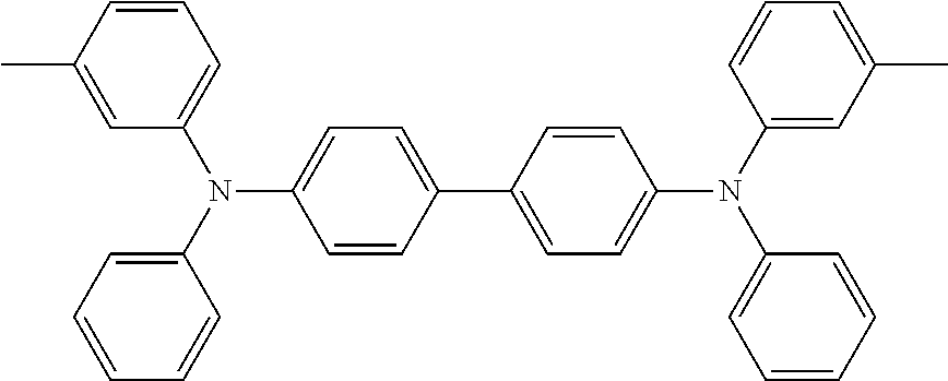 |
Appl. Phys. Lett. 51, 913 (1987) |
 |
US5061569 | |
 |
EP650955 | |
 |
J. Mater. Chem. 3, 319 (1993) | |
 |
Appl. Phys. Lett. 90, 183503 (2007) | |
 |
Appl. Phys. Lett. 90, 183503 (2007) | |
| Triaylamine on spirofluorene core |
 |
Synth. Met. 91, 209 (1997) |
| Arylamine carbazole compounds |
 |
Adv. Mater. 6, 677 (1994) |
| Indolocarbazoles |
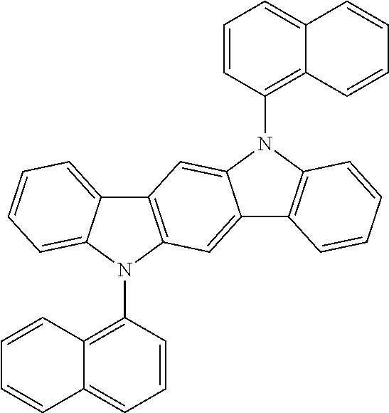 |
Synth. Met. 111, 421 (2000) |
| Isoindole compounds |
 |
Chem. Mater. 15, 3148 (2003) |
| Phosphorescent OLED host materials |
| Red hosts |
| Arylcarbazoles |
 |
Appl. Phys. Lett. 78, 1622 (2001) |
| Metal 8-hydroxyquinolates (e.g., Alq3, BAlq) |
 |
Nature 395, 151 (1998) |
 |
US20060202194 | |
 |
WO2005014551 | |
| Metal phenoxybenzothiazole compounds |
 |
Appl. Phys. Lett. 90, 123509 (2007) |
| Conjugated oligomers and polymers (e.g., polyfluorene) |
 |
Org. Electron. 1, 15 (2000) |
| Green hosts |
| Arylcarbazoles |
 |
Appl. Phys. Lett. 78, 1622 (2001) |
 |
US2003175553 | |
 |
WO2001039234 | |
| Aryltriphenylene compounds |
 |
US20060280965 |
 |
US20060280965 | |
| Polymers (e.g., PVK) |
 |
Appl. Phys. Lett. 77, 2280 (2000) |
| Spirofluorene compounds |
 |
WO2004093207 |
| Metal phenoxybenzooxazole compounds |
 |
WO05089025 |
 |
WO06132173 | |
 |
JP200511610 | |
| Spirofluorene- carbazole compounds |
 |
JP2007254297 |
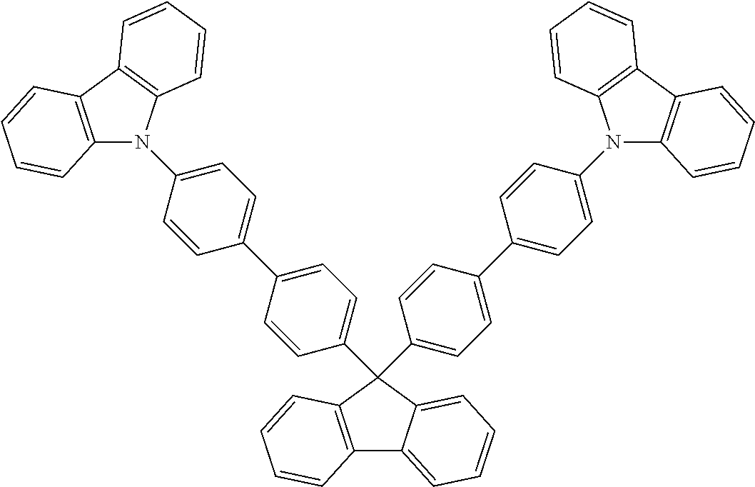 |
JP2007254297 | |
| Indolocabazoles |
 |
WO07063796 |
 |
WO07063754 | |
| 5-member ring electron deficient heterocycles (e.g., triazole, oxadiazole) |
 |
J. Appl. Phys. 90, 5048 (2001) |
 |
WO04107822 | |
| Metal phenoxypyridine compounds |
 |
WO05030900 |
| Blue hosts |
| Arylcarbazoles |
 |
Appl. Phys. Lett, 82, 2422 (2003) |
 |
US20070190359 | |
| Dibenzothiophene- carbazole compounds |
 |
WO2006114966 |
| Phosphorescent dopants |
| Red dopants |
| Heavy metal porphyrins (e.g., PtOEP) |
 |
Nature 395, 151 (1998) |
| Iridium(III) organometallic complexes |
 |
Appl. Phys. Lett. 78, 1622 (2001) |
 |
US06835469 | |
 |
US06835469 | |
 |
US20060202194 | |
 |
US20060202194 | |
 |
US07087321 | |
 |
US07087321 | |
 |
Adv. Mater. 19, 739 (2007) | |
| Platinum(II) organometallic complexes |
 |
WO2003040257 |
| Osminum(III) complexes |
 |
Chem. Mater. 17, 3532 (2005) |
| Ruthenium(II) complexes |
 |
Adv. Mater. 17, 1059 (2005) |
| Green dopants |
| Iridium(III) organometallic complexes |
 |
Inorg. Chem. 40, 1704 (2001) |
 |
US2002034656 | |
 |
US06687266 | |
 |
Chem. Mater. 16, 2480 (2004) | |
 |
US2007190359 | |
 |
US 2006008670 JP2007123392 | |
 |
Adv. Mater. 16, 2003 (2004) | |
 |
Angew. Chem. Int. Ed. 2006, 45, 7800 | |
| Pt(II) organometallic complexes |
 |
Appl. Phys. Lett. 86, 153505 (2005) |
 |
Appl. Phys. Lett. 86, 153505 (2005) | |
 |
Chem. Lett. 34, 592 (2005) | |
| Gold complexes |
 |
Chem. Commun. 2906 (2005) |
| Rhenium(III) complexes |
 |
Inorg. Chem. 42, 1248 (2003) |
| Blue dopants |
| Iridium(III) organometallic complexes |
 |
WO2002002714 |
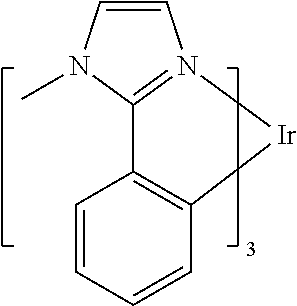 |
WO2006009024 | |
 |
US2006251923 | |
 |
WO2006056418, US2005260441 | |
 |
US2007190359 | |
 |
US2002134984 | |
 |
Angew. Chem. Int. Ed. 47, 1 (2008) | |
 |
Chem. Mater. 18, 5119 (2006) | |
 |
Inorg. Chem. 46, 4308 (2007) | |
 |
WO05123873 | |
 |
WO05123873 | |
 |
WO07004380 | |
 |
WO06082742 | |
| Osmium(II) complexes |
 |
US2005260449 |
 |
Organometallics 23, 3745 (2004) | |
| Gold complexes |
|
Appl. Phys. Lett.74,1361 (1999) |
| Platinum(II) complexes |
 |
WO06098120, WO06103874 |
| Exciton/hole blocking layer materials |
| Bathocuprine compounds (e.g., BCP, BPhen) |
 |
Appl. Phys. Lett. 75, 4 (1999) |
 |
Appl. Phys. Lett. 79, 449 (2001) | |
| Metal 8-hydroxyquinolates (e.g., BAlq) |
 |
Appl. Phys. Lett. 81, 162 (2002) |
| 5-member ring electron deficient heterocycles such as triazole, oxadiazole, imidazole, benzoimidazole |
 |
Appl. Phys. Lett. 81, 162 (2002) |
| Triphenylene compounds |
 |
US20050025993 |
| Fluorinated aromatic compounds |
 |
Appl. Phys. Lett. 79, 156 (2001) |
| Electron transporting materials |
| Anthracene- benzoimidazole compounds |
 |
WO03060956 |
| Anthracene- benzothiazole compounds |
 |
Appl. Phys. Lett. 89, 063504 (2006) |
| Metal 8-hydroxyquinolates (e.g., Alq3) |
 |
Appl. Phys. Lett. 51, 913 (1987) |
| Metal hydroxybenoquinolates |
 |
Chem. Lett. 5, 905 (1993) |
| Bathocuprine compounds such as BCP, BPhen, etc |
 |
Appl. Phys. Lett. 91, 263503 (2007) |
 |
Appl. Phys. Lett. 79, 449 (2001) | |
| 5-member ring electron deficient heterocycles (e.g.,triazole, oxadiazole, imidazole, benzoimidazole) |
 |
Appl. Phys. Lett. 74, 865 (1999) |
 |
Appl. Phys. Lett. 55, 1489 (1989) | |
 |
Jpn. J. Apply. Phys. 32, L917 (1993) | |
| Silole compounds |
 |
Org. Electron. 4, 113 (2003) |
| Arylborane compounds |
 |
J. Am. Chem. Soc. 120, 9714 (1998) |
| Fluorinated aromatic compounds |
 |
J. Am. Chem. Soc. 122, 1832 (2000) |


| TABLE 2 | |||||
| EML | |||||
| Example | HIL | HTL | (300 Å, doping %) | BL | ETL |
| Example 1 | |
NPD 300 | H1 | Compound | 1 15% | H1 50 Å | Alq 400 Å | |
| Example 2 | |
NPD 300 | H1 | Compound | 2 15% | H1 50 Å | Alq 400 Å | |
| Example 3 | |
NPD 300 | H1 | Compound | 3 15% | H1 50 Å | Alq 400 Å | |
| Example 4 | |
NPD 300 | H1 | Compound | 5 15% | H1 50 Å | Alq 400 Å | |
| Example 5 | |
NPD 300 | H2 | Compound | 1 15% | H1 50 Å | Alq 400 | |
| Comparative | C1 | |||||||
| 100 Å | NPD 300 Å | H1 | E1 15% | H1 50 Å | Alq 400 Å | |||
| Example 1 | ||||||||
| | C1 | 100 Å | NPD 300 Å | H1 | E2 15% | H1 50 Å | Alq 400 Å | |
| Example 2 | ||||||||
| | C1 | 100 Å | NPD 300 | H3 | Compound | 1 15% | H1 50 Å | Alq 400 Å |
| Example 3 | ||||||||
| TABLE 3 | ||||||
| At 1000 cd/m2 | At 2000 cd/m2 | |||||
| 1931 CIE | FWHM | V | LE | EQE | PE | LT80% |
| Example | x | y | λmax | (nm) | (V) | (Cd/A) | (%) | (lm/W) | (h) |
| Example 1 | 0.177 | 0.383 | 474 | 54 | 6.7 | 38.7 | 17.3 | 18.1 | 420 |
| Example 2 | 0.179 | 0.385 | 474 | 56 | 7.2 | 32.1 | 14.2 | 14.0 | 220 |
| Example 3 | 0.176 | 0.379 | 474 | 56 | 8.1 | 24.5 | 11 | 9.5 | 105 |
| Example 4 | 0.182 | 0.400 | 476 | 56 | 7.6 | 26.3 | 11.5 | 10.8 | 50 |
| Example 5 | 0.179 | 0.385 | 474 | 56 | 7.5 | 27.1 | 12 | 11.3 | 250 |
| Comparative | 0.175 | 0.384 | 474 | 56 | 5.9 | 40.2 | 18.4 | 21.3 | 155 |
| Example 1 | |||||||||
| Comparative | 0.202 | 0.464 | 482 | 60 | 7 | 24 | 9.5 | 10.8 | 360 |
| Example 2 | |||||||||
| Comparative | 0.174 | 0.377 | 474 | 54 | 6.9 | 40.3 | 18.1 | 18.3 | 210 |
| Example 3 | |||||||||
| TABLE 4 | |||
| 77K LT | |||
| Compound | (μs) | ||
| |
2.5 | ||
| |
2.4 | ||
| |
2.5 | ||
| |
2.3 | ||
| E1 | 3.2 | ||
| E2 | 3.3 | ||
Claims (4)

Priority Applications (3)
| Application Number | Priority Date | Filing Date | Title |
|---|---|---|---|
| US12/869,284 US8586204B2 (en) | 2007-12-28 | 2010-08-26 | Phosphorescent emitters and host materials with improved stability |
| US14/054,239 US20140042413A1 (en) | 2007-12-28 | 2013-10-15 | Phosphorescent emitters and host materials with improved stability |
| US15/395,470 US9735377B2 (en) | 2005-05-06 | 2016-12-30 | Phosphorescent emitters and host materials with improved stability |
Applications Claiming Priority (4)
| Application Number | Priority Date | Filing Date | Title |
|---|---|---|---|
| US1748007P | 2007-12-28 | 2007-12-28 | |
| US12/208,907 US8007927B2 (en) | 2007-12-28 | 2008-09-11 | Dibenzothiophene-containing materials in phosphorescent light emitting diodes |
| US23993209P | 2009-09-04 | 2009-09-04 | |
| US12/869,284 US8586204B2 (en) | 2007-12-28 | 2010-08-26 | Phosphorescent emitters and host materials with improved stability |
Related Parent Applications (2)
| Application Number | Title | Priority Date | Filing Date |
|---|---|---|---|
| US12/208,907 Continuation-In-Part US8007927B2 (en) | 2005-05-06 | 2008-09-11 | Dibenzothiophene-containing materials in phosphorescent light emitting diodes |
| US15/395,470 Continuation-In-Part US9735377B2 (en) | 2005-05-06 | 2016-12-30 | Phosphorescent emitters and host materials with improved stability |
Related Child Applications (1)
| Application Number | Title | Priority Date | Filing Date |
|---|---|---|---|
| US14/054,239 Division US20140042413A1 (en) | 2005-05-06 | 2013-10-15 | Phosphorescent emitters and host materials with improved stability |
Publications (2)
| Publication Number | Publication Date |
|---|---|
| US20110057559A1 US20110057559A1 (en) | 2011-03-10 |
| US8586204B2 true US8586204B2 (en) | 2013-11-19 |
Family
ID=43647177
Family Applications (3)
| Application Number | Title | Priority Date | Filing Date |
|---|---|---|---|
| US12/869,284 Active 2029-12-08 US8586204B2 (en) | 2005-05-06 | 2010-08-26 | Phosphorescent emitters and host materials with improved stability |
| US14/054,239 Abandoned US20140042413A1 (en) | 2005-05-06 | 2013-10-15 | Phosphorescent emitters and host materials with improved stability |
| US15/395,470 Active US9735377B2 (en) | 2005-05-06 | 2016-12-30 | Phosphorescent emitters and host materials with improved stability |
Family Applications After (2)
| Application Number | Title | Priority Date | Filing Date |
|---|---|---|---|
| US14/054,239 Abandoned US20140042413A1 (en) | 2005-05-06 | 2013-10-15 | Phosphorescent emitters and host materials with improved stability |
| US15/395,470 Active US9735377B2 (en) | 2005-05-06 | 2016-12-30 | Phosphorescent emitters and host materials with improved stability |
Country Status (1)
| Country | Link |
|---|---|
| US (3) | US8586204B2 (en) |
Cited By (21)
| Publication number | Priority date | Publication date | Assignee | Title |
|---|---|---|---|---|
| US20100301383A1 (en) * | 2009-05-29 | 2010-12-02 | Semiconductor Energy Laboratory Co., Ltd. | Light-Emitting Element, Light-Emitting Device, and Method for Manufacturing the Same |
| US20100301382A1 (en) * | 2009-05-29 | 2010-12-02 | Semiconductor Energy Laboratory Co., Ltd. | Light-Emitting Element, Light-Emitting Device, Lighting Device, and Electronic Appliance |
| US20110050093A1 (en) * | 2009-08-31 | 2011-03-03 | Fujifilm Corporation | Method of forming metal complex compound, and organic electroluminescence device |
| US20140042413A1 (en) * | 2007-12-28 | 2014-02-13 | Universal Display Corporation | Phosphorescent emitters and host materials with improved stability |
| US8993125B2 (en) | 2010-05-21 | 2015-03-31 | Semiconductor Energy Laboratory Co., Ltd. | Triazole derivative, and light-emitting element, light-emitting device, electronic device and lighting device using the triazole derivative |
| US9065058B2 (en) | 2010-09-10 | 2015-06-23 | Semiconductor Energy Laboratory Co., Ltd. | Light-emitting element and electronic device |
| US9309223B2 (en) | 2011-07-08 | 2016-04-12 | Semiconductor Energy Laboratory Co., Ltd. | Heterocyclic compound, light-emitting element, light-emitting device, electronic device, and lighting device |
| US9406893B2 (en) | 2010-09-09 | 2016-08-02 | Semiconductor Energy Laboratory Co., Ltd. | Heterocyclic compound, light-emitting element, light-emitting device, electronic device, and lighting device |
| US9406889B2 (en) | 2010-10-29 | 2016-08-02 | Semiconductor Energy Laboratory Co., Ltd. | Phenanthrene compound, light-emitting element, light-emitting device, electronic device, and lighting device |
| US9496505B2 (en) | 2010-10-04 | 2016-11-15 | Semiconductor Energy Laboratory Co., Ltd. | Composite material, light-emitting element, light-emitting device, electronic device, and lighting device |
| US9799834B2 (en) | 2011-08-18 | 2017-10-24 | Semiconductor Energy Laboratory Co., Ltd. | Carbazole compound light-emitting element, light-emitting device, electronic device, and lighting device |
| US9831435B2 (en) | 2011-03-23 | 2017-11-28 | Semiconductor Energy Laboratory Co., Ltd. | Composite material, light-emitting element, light-emitting device, electronic device, and lighting device |
| US9905782B2 (en) | 2013-03-26 | 2018-02-27 | Semiconductor Energy Laboratory Co., Ltd. | Light-emitting element, compound, organic compound, display module, lighting module, light-emitting device, display device, lighting device, and electronic device |
| US9960368B2 (en) | 2011-02-01 | 2018-05-01 | Semiconductor Energy Laboratory Co., Ltd. | Heterocyclic compound |
| US10071993B2 (en) | 2010-09-21 | 2018-09-11 | Semiconductor Energy Laboratory Co., Ltd. | Carbazole derivative, light-emitting element material and organic semiconductor material |
| US10308841B2 (en) * | 2014-05-30 | 2019-06-04 | Henkel Ag & Co. Kgaa | Process and apparatus for detaching a display module bonded by a liquid optically clear adhesive |
| US10424745B2 (en) | 2009-11-02 | 2019-09-24 | Semiconductor Energy Laboratory Co., Ltd. | Organometallic complex, light-emitting element, display device, electronic device, and lighting device |
| US10586931B2 (en) | 2015-12-25 | 2020-03-10 | Semiconductor Energy Laboratory Co., Ltd. | Compound, light-emitting element, display device, electronic device, and lighting device |
| US10586932B2 (en) | 2015-05-29 | 2020-03-10 | Semiconductor Energy Laboratory Co., Ltd. | Light-emitting element, light-emitting device, display device, electronic device, and lighting device |
| US11107995B2 (en) | 2016-06-24 | 2021-08-31 | Semiconductor Energy Laboratory Co., Ltd. | Organic compound, light-emitting element, light-emitting device, electronic device, and lighting device |
| US11404650B2 (en) * | 2005-05-06 | 2022-08-02 | Universal Display Corporation | Stability OLED materials and devices |
Families Citing this family (171)
| Publication number | Priority date | Publication date | Assignee | Title |
|---|---|---|---|---|
| US8007927B2 (en) | 2007-12-28 | 2011-08-30 | Universal Display Corporation | Dibenzothiophene-containing materials in phosphorescent light emitting diodes |
| KR20210130847A (en) | 2006-02-10 | 2021-11-01 | 유니버셜 디스플레이 코포레이션 | METAL COMPLEXES OF CYCLOMETALLATED IMIDAZO[1,2-f]PHENANTHRIDINE AND DIIMIDAZO[1,2-A:1',2'-C]QUINAZOLINE LIGANDS AND ISOELECTRONIC AND BENZANNULATED ANALOGS THEREOF |
| US8288187B2 (en) | 2010-01-20 | 2012-10-16 | Universal Display Corporation | Electroluminescent devices for lighting applications |
| JP2012006878A (en) * | 2010-06-25 | 2012-01-12 | Mitsubishi Chemicals Corp | Organometallic complex, luminescent material, organic electroluminescent element material, organometallic complex-containing composition, organic electroluminescent element, organic el display, and organic el illumination |
| JP5650961B2 (en) * | 2010-09-08 | 2015-01-07 | ユー・ディー・シー アイルランド リミテッド | Organic electroluminescent device and material for organic electroluminescent device having dibenzothiophene structure or dibenzofuran structure |
| US8637858B2 (en) | 2010-09-24 | 2014-01-28 | Novaled Ag | Tandem white OLED |
| TW201233675A (en) * | 2011-01-07 | 2012-08-16 | Idemitsu Kosan Co | Imidazole compound production method, imidazole compound, imidazole-based compound, organic metal complex, material for organic electroluminescent element, organic electroluminescent element, display device, and lighting device |
| US9155158B2 (en) * | 2011-04-01 | 2015-10-06 | Semiconductor Energy Laboratory Co., Ltd. | Organometallic complex, light-emitting element, display device, electronic device, and lighting device |
| US8773013B2 (en) | 2011-05-12 | 2014-07-08 | Universal Display Corporation | Three dimensional OLED lamps |
| US8907560B2 (en) | 2011-05-12 | 2014-12-09 | Universal Display Corporation | Dynamic OLED lighting |
| KR102119353B1 (en) * | 2011-06-08 | 2020-06-29 | 유니버셜 디스플레이 코포레이션 | Heteroleptic iridium carbene complexes and light emitting device using them |
| US8764239B2 (en) | 2011-08-16 | 2014-07-01 | Universal Display Corporation | Dynamic stretchable OLED lamp |
| JP5742586B2 (en) | 2011-08-25 | 2015-07-01 | コニカミノルタ株式会社 | Organic electroluminescence element, lighting device and display device |
| WO2013031662A1 (en) * | 2011-08-26 | 2013-03-07 | コニカミノルタホールディングス株式会社 | Organic electroluminescence element, illumination device, and display device |
| JP5987830B2 (en) * | 2011-08-30 | 2016-09-07 | コニカミノルタ株式会社 | Organic electroluminescence device |
| JP2013058647A (en) * | 2011-09-09 | 2013-03-28 | Konica Minolta Holdings Inc | White organic electroluminescent element |
| JP2013062201A (en) * | 2011-09-15 | 2013-04-04 | Konica Minolta Holdings Inc | Method for manufacturing organic electroluminescent element, and organic electroluminescent element |
| WO2013042460A1 (en) * | 2011-09-20 | 2013-03-28 | コニカミノルタホールディングス株式会社 | Organic electroluminescent element, lighting device and display device |
| WO2013048419A1 (en) | 2011-09-29 | 2013-04-04 | Universal Display Corporation | LAMP WITH MULTIPLE FLEXIBLE OLEDs |
| WO2013058087A1 (en) * | 2011-10-21 | 2013-04-25 | コニカミノルタ株式会社 | Organic electroluminscent element |
| JP6056763B2 (en) | 2011-10-21 | 2017-01-11 | コニカミノルタ株式会社 | Organic electroluminescence device |
| JP5817469B2 (en) * | 2011-11-25 | 2015-11-18 | コニカミノルタ株式会社 | Organic electroluminescence device |
| US9722183B2 (en) | 2011-11-30 | 2017-08-01 | Novaled Gmbh | Display |
| JP6197650B2 (en) * | 2011-12-20 | 2017-09-20 | コニカミノルタ株式会社 | Organic EL device |
| CN104145002A (en) * | 2011-12-28 | 2014-11-12 | 索尔维公司 | Heteroleptic light-emiiting complexes |
| EP2674468A1 (en) | 2012-06-15 | 2013-12-18 | Solvay Sa | Heteroleptic light emitting complexes |
| KR102012047B1 (en) | 2012-01-06 | 2019-08-19 | 유니버셜 디스플레이 코포레이션 | Highly efficient phosphorescent materials |
| US10211413B2 (en) | 2012-01-17 | 2019-02-19 | Universal Display Corporation | Organic electroluminescent materials and devices |
| JP5978843B2 (en) * | 2012-02-02 | 2016-08-24 | コニカミノルタ株式会社 | Iridium complex compound, organic electroluminescence device material, organic electroluminescence device, lighting device and display device |
| JP6020473B2 (en) * | 2012-02-02 | 2016-11-02 | コニカミノルタ株式会社 | Iridium complex compound, organic electroluminescence device material, organic electroluminescence device, lighting device and display device |
| US9837625B2 (en) | 2012-02-29 | 2017-12-05 | Konica Minolta, Inc. | Organic electroluminescent element |
| US9386657B2 (en) | 2012-03-15 | 2016-07-05 | Universal Display Corporation | Organic Electroluminescent materials and devices |
| JP6024744B2 (en) * | 2012-04-03 | 2016-11-16 | コニカミノルタ株式会社 | Organic electroluminescence device |
| KR101973834B1 (en) | 2012-04-20 | 2019-04-29 | 코니카 미놀타 가부시키가이샤 | Organic electroluminescent element |
| WO2013161739A1 (en) * | 2012-04-23 | 2013-10-31 | コニカミノルタ株式会社 | Organic electroluminescence element, illumination device and display device |
| KR101701584B1 (en) | 2012-04-23 | 2017-02-01 | 코니카 미놀타 가부시키가이샤 | Organic electroluminescent element |
| WO2013168534A1 (en) * | 2012-05-09 | 2013-11-14 | コニカミノルタ株式会社 | Organic electroluminescence element, production method for organic electroluminescence element, display device, and illumination device |
| JP5849853B2 (en) * | 2012-05-10 | 2016-02-03 | コニカミノルタ株式会社 | Organic electroluminescence element, display device and lighting device |
| US9773985B2 (en) * | 2012-05-21 | 2017-09-26 | Universal Display Corporation | Organic electroluminescent materials and devices |
| JP5880274B2 (en) | 2012-05-21 | 2016-03-08 | コニカミノルタ株式会社 | Organic electroluminescence element, lighting device and display device |
| JP2013245179A (en) * | 2012-05-25 | 2013-12-09 | Konica Minolta Inc | Metal complex, organic electroluminescent element, display and illumination apparatus |
| US9540329B2 (en) | 2012-07-19 | 2017-01-10 | Universal Display Corporation | Organic electroluminescent materials and devices |
| WO2014024668A1 (en) | 2012-08-07 | 2014-02-13 | コニカミノルタ株式会社 | Organic electroluminescent element, lighting device and display device |
| WO2014034584A1 (en) * | 2012-08-27 | 2014-03-06 | コニカミノルタ株式会社 | Organic electroluminescent element, illuminator, and display device |
| EP2894686B1 (en) | 2012-09-04 | 2018-01-03 | Konica Minolta, Inc. | Organic electroluminescent element, lighting device and display device |
| EP2897959B1 (en) | 2012-09-20 | 2017-12-20 | UDC Ireland Limited | Azadibenzofurans for electronic applications |
| US9252363B2 (en) | 2012-10-04 | 2016-02-02 | Universal Display Corporation | Aryloxyalkylcarboxylate solvent compositions for inkjet printing of organic layers |
| JP5900292B2 (en) * | 2012-11-06 | 2016-04-06 | コニカミノルタ株式会社 | Method for producing iminochloride derivative and method for producing phenylimidazole derivative |
| TWI597285B (en) | 2012-11-06 | 2017-09-01 | Udc愛爾蘭責任有限公司 | Phenoxasiline based compounds for electronic application |
| GB2508408A (en) * | 2012-11-30 | 2014-06-04 | Cambridge Display Tech Ltd | Phosphorescent light-emitting 1,2,4-triazine compounds |
| US9196860B2 (en) | 2012-12-04 | 2015-11-24 | Universal Display Corporation | Compounds for triplet-triplet annihilation upconversion |
| US8716484B1 (en) | 2012-12-05 | 2014-05-06 | Universal Display Corporation | Hole transporting materials with twisted aryl groups |
| US9653691B2 (en) | 2012-12-12 | 2017-05-16 | Universal Display Corporation | Phosphorescence-sensitizing fluorescence material system |
| KR102073138B1 (en) * | 2012-12-17 | 2020-02-04 | 엘지디스플레이 주식회사 | Blue phosphorescence composition and organic light emitting diode comprising the same |
| US10374172B2 (en) | 2013-03-20 | 2019-08-06 | Udc Ireland Limited | Azabenzimidazole carbene complexes as efficiency booster in OLEDs |
| US10468610B2 (en) | 2013-03-29 | 2019-11-05 | Konica Minolta, Inc. | Isomer-mixture metal complex composition, organic electroluminescent element, illuminator, and display device |
| US20140332777A1 (en) * | 2013-05-09 | 2014-11-13 | Electronics And Telecommunications Research Institute | Phosphorescent host material and organic light-emitting device including the same |
| JP5403179B1 (en) | 2013-05-22 | 2014-01-29 | コニカミノルタ株式会社 | Charge transfer thin film |
| WO2014189072A1 (en) | 2013-05-22 | 2014-11-27 | コニカミノルタ株式会社 | Electronic device, organic electroluminescent element, organic thin-film solar cell, and dye-sensitized solar cell |
| US20160372687A1 (en) | 2013-07-02 | 2016-12-22 | Basf Se | Monosubstituted diazabenzimidazole carbene metal complexes for use in organic light emitting diodes |
| CN105392863B (en) | 2013-07-17 | 2018-08-03 | 住友化学株式会社 | Composition and the light-emitting component for using the composition |
| US20150028290A1 (en) * | 2013-07-25 | 2015-01-29 | Universal Display Corporation | Heteroleptic osmium complex and method of making the same |
| EP3239161A1 (en) | 2013-07-31 | 2017-11-01 | UDC Ireland Limited | Luminescent diazabenzimidazole carbene metal complexes |
| EP2840622B1 (en) | 2013-08-19 | 2019-02-13 | Novaled GmbH | Electronic or optoelectronic device comprising an anchored thin molecular layer, process for its preparation and compound used therein |
| WO2015046452A1 (en) | 2013-09-27 | 2015-04-02 | コニカミノルタ株式会社 | Iridium complex, method for producing iridium complex, organic electroluminescence element, display device and illumination device |
| EP3063153B1 (en) | 2013-10-31 | 2018-03-07 | Idemitsu Kosan Co., Ltd. | Azadibenzothiophenes for electronic applications |
| US9876173B2 (en) | 2013-12-09 | 2018-01-23 | Universal Display Corporation | Organic electroluminescent materials and devices |
| JP6462698B2 (en) | 2013-12-20 | 2019-01-30 | ユー・ディー・シー アイルランド リミテッド | High efficiency OLED device with very short decay time |
| JP2015174824A (en) * | 2014-03-13 | 2015-10-05 | 住友化学株式会社 | Metal complex and light emitting element prepared using the same |
| KR102332743B1 (en) | 2014-03-17 | 2021-11-30 | 스미또모 가가꾸 가부시키가이샤 | Metal complex and light-emitting element using same |
| KR102330660B1 (en) | 2014-03-31 | 2021-11-24 | 유디씨 아일랜드 리미티드 | Metal complexes, comprising carbene ligands having an o-substituted non-cyclometalated aryl group and their use in organic light emitting diodes |
| US9450198B2 (en) | 2014-04-15 | 2016-09-20 | Universal Display Corporation | Organic electroluminescent materials and devices |
| EP3174885B1 (en) | 2014-07-28 | 2019-10-02 | Idemitsu Kosan Co., Ltd. | 2,9-functionalized benzimidazolo[1,2-a]benzimidazoles as hosts for organic light emitting diodes (oleds) |
| EP2982676B1 (en) | 2014-08-07 | 2018-04-11 | Idemitsu Kosan Co., Ltd. | Benzimidazo[2,1-B]benzoxazoles for electronic applications |
| EP2993215B1 (en) | 2014-09-04 | 2019-06-19 | Idemitsu Kosan Co., Ltd. | Azabenzimidazo[2,1-a]benzimidazoles for electronic applications |
| EP3015469B1 (en) | 2014-10-30 | 2018-12-19 | Idemitsu Kosan Co., Ltd. | 5-(benzimidazol-2-yl)benzimidazo[1,2-a]benzimidazoles for electronic applications |
| CN104447433A (en) * | 2014-11-11 | 2015-03-25 | 常州大学 | Method for synthesizing 3,5-dibromoparatoluensulfonyl chloride |
| WO2016079667A1 (en) | 2014-11-17 | 2016-05-26 | Idemitsu Kosan Co., Ltd. | Indole derivatives for electronic applications |
| EP3034507A1 (en) | 2014-12-15 | 2016-06-22 | Idemitsu Kosan Co., Ltd | 1-functionalized dibenzofurans and dibenzothiophenes for organic light emitting diodes (OLEDs) |
| EP3034506A1 (en) | 2014-12-15 | 2016-06-22 | Idemitsu Kosan Co., Ltd | 4-functionalized carbazole derivatives for electronic applications |
| EP3054498B1 (en) | 2015-02-06 | 2017-09-20 | Idemitsu Kosan Co., Ltd. | Bisimidazodiazocines |
| EP3053918B1 (en) | 2015-02-06 | 2018-04-11 | Idemitsu Kosan Co., Ltd. | 2-carbazole substituted benzimidazoles for electronic applications |
| US9929361B2 (en) | 2015-02-16 | 2018-03-27 | Universal Display Corporation | Organic electroluminescent materials and devices |
| EP3061759B1 (en) | 2015-02-24 | 2019-12-25 | Idemitsu Kosan Co., Ltd | Nitrile substituted dibenzofurans |
| US11056657B2 (en) | 2015-02-27 | 2021-07-06 | University Display Corporation | Organic electroluminescent materials and devices |
| EP3070144B1 (en) | 2015-03-17 | 2018-02-28 | Idemitsu Kosan Co., Ltd. | Seven-membered ring compounds |
| EP3072943B1 (en) | 2015-03-26 | 2018-05-02 | Idemitsu Kosan Co., Ltd. | Dibenzofuran/carbazole-substituted benzonitriles |
| EP3075737B1 (en) | 2015-03-31 | 2019-12-04 | Idemitsu Kosan Co., Ltd | Benzimidazolo[1,2-a]benzimidazole carrying aryl- or heteroarylnitril groups for organic light emitting diodes |
| US9859510B2 (en) | 2015-05-15 | 2018-01-02 | Universal Display Corporation | Organic electroluminescent materials and devices |
| US10418568B2 (en) | 2015-06-01 | 2019-09-17 | Universal Display Corporation | Organic electroluminescent materials and devices |
| CN107735880B (en) | 2015-06-03 | 2020-07-10 | Udc 爱尔兰有限责任公司 | Efficient O L ED device with extremely short decay time |
| US11127905B2 (en) | 2015-07-29 | 2021-09-21 | Universal Display Corporation | Organic electroluminescent materials and devices |
| US10361381B2 (en) | 2015-09-03 | 2019-07-23 | Universal Display Corporation | Organic electroluminescent materials and devices |
| US20180269407A1 (en) | 2015-10-01 | 2018-09-20 | Idemitsu Kosan Co., Ltd. | Benzimidazolo[1,2-a]benzimidazole carrying triazine groups for organic light emitting diodes |
| EP3150604B1 (en) | 2015-10-01 | 2021-07-14 | Idemitsu Kosan Co., Ltd. | Benzimidazolo[1,2-a]benzimidazole carrying benzimidazolo[1,2-a]benzimidazolylyl groups, carbazolyl groups, benzofurane groups or benzothiophene groups for organic light emitting diodes |
| EP3150606B1 (en) | 2015-10-01 | 2019-08-14 | Idemitsu Kosan Co., Ltd. | Benzimidazolo[1,2-a]benzimidazoles carrying benzofurane or benzothiophene groups for organic light emitting diodes |
| EP3356368B1 (en) | 2015-10-01 | 2021-07-21 | Idemitsu Kosan Co., Ltd | Benzimidazolo[1,2-a]benzimidazole carrying benzimidazolo[1,2-a]benzimidazolyl groups, carbazolyl groups, benzofurane groups or benzothiophene groups for organic light emitting diodes |
| KR20180079328A (en) | 2015-11-04 | 2018-07-10 | 이데미쓰 고산 가부시키가이샤 | Benzimidazole condensed heteroaryl |
| US11174258B2 (en) | 2015-12-04 | 2021-11-16 | Idemitsu Kosan Co., Ltd. | Benzimidazolo[1,2-a]benzimidazole derivatives for organic light emitting diodes |
| KR20180091026A (en) * | 2015-12-07 | 2018-08-14 | 스미또모 가가꾸 가부시키가이샤 | Light emitting element |
| JP6375069B2 (en) | 2015-12-21 | 2018-08-15 | 出光興産株式会社 | Phenylquinazoline bridged with heteroatoms |
| JP6160685B2 (en) * | 2015-12-24 | 2017-07-12 | コニカミノルタ株式会社 | Organic electroluminescence element, lighting device and display device |
| KR102345329B1 (en) | 2016-01-29 | 2022-01-03 | 스미또모 가가꾸 가부시키가이샤 | Composition, phosphorescent compound, and light-emitting element |
| US20170229663A1 (en) | 2016-02-09 | 2017-08-10 | Universal Display Corporation | Organic electroluminescent materials and devices |
| US10236456B2 (en) | 2016-04-11 | 2019-03-19 | Universal Display Corporation | Organic electroluminescent materials and devices |
| WO2017178864A1 (en) | 2016-04-12 | 2017-10-19 | Idemitsu Kosan Co., Ltd. | Seven-membered ring compounds |
| US10862054B2 (en) | 2016-06-20 | 2020-12-08 | Universal Display Corporation | Organic electroluminescent materials and devices |
| US10672997B2 (en) | 2016-06-20 | 2020-06-02 | Universal Display Corporation | Organic electroluminescent materials and devices |
| US11482683B2 (en) | 2016-06-20 | 2022-10-25 | Universal Display Corporation | Organic electroluminescent materials and devices |
| US11691983B2 (en) | 2016-06-22 | 2023-07-04 | Idemitsu Kosan Co., Ltd. | Specifically substituted benzofuro- and benzothienoquinolines for organic light emitting diodes |
| CN107799658B (en) * | 2016-08-29 | 2021-05-28 | 株式会社半导体能源研究所 | Light-emitting element, light-emitting device, electronic device, lighting device, and organometallic complex |
| US10608186B2 (en) | 2016-09-14 | 2020-03-31 | Universal Display Corporation | Organic electroluminescent materials and devices |
| US10680187B2 (en) | 2016-09-23 | 2020-06-09 | Universal Display Corporation | Organic electroluminescent materials and devices |
| US11196010B2 (en) | 2016-10-03 | 2021-12-07 | Universal Display Corporation | Organic electroluminescent materials and devices |
| US11011709B2 (en) | 2016-10-07 | 2021-05-18 | Universal Display Corporation | Organic electroluminescent materials and devices |
| US20180130956A1 (en) | 2016-11-09 | 2018-05-10 | Universal Display Corporation | Organic electroluminescent materials and devices |
| US10680188B2 (en) | 2016-11-11 | 2020-06-09 | Universal Display Corporation | Organic electroluminescent materials and devices |
| US11780865B2 (en) | 2017-01-09 | 2023-10-10 | Universal Display Corporation | Organic electroluminescent materials and devices |
| US10844085B2 (en) | 2017-03-29 | 2020-11-24 | Universal Display Corporation | Organic electroluminescent materials and devices |
| US10944060B2 (en) | 2017-05-11 | 2021-03-09 | Universal Display Corporation | Organic electroluminescent materials and devices |
| JP6468314B2 (en) * | 2017-06-15 | 2019-02-13 | コニカミノルタ株式会社 | Organic electroluminescence element, lighting device and display device |
| US20180370999A1 (en) | 2017-06-23 | 2018-12-27 | Universal Display Corporation | Organic electroluminescent materials and devices |
| US11228010B2 (en) | 2017-07-26 | 2022-01-18 | Universal Display Corporation | Organic electroluminescent materials and devices |
| US11744142B2 (en) | 2017-08-10 | 2023-08-29 | Universal Display Corporation | Organic electroluminescent materials and devices |
| EP3466954A1 (en) | 2017-10-04 | 2019-04-10 | Idemitsu Kosan Co., Ltd. | Fused phenylquinazolines bridged with a heteroatom |
| KR102452949B1 (en) * | 2017-11-20 | 2022-10-12 | 삼성전자주식회사 | Organic light emitting device |
| US20190161504A1 (en) | 2017-11-28 | 2019-05-30 | University Of Southern California | Carbene compounds and organic electroluminescent devices |
| EP3492480B1 (en) | 2017-11-29 | 2021-10-20 | Universal Display Corporation | Organic electroluminescent materials and devices |
| US11937503B2 (en) | 2017-11-30 | 2024-03-19 | Universal Display Corporation | Organic electroluminescent materials and devices |
| US11542289B2 (en) | 2018-01-26 | 2023-01-03 | Universal Display Corporation | Organic electroluminescent materials and devices |
| EP3604477A1 (en) | 2018-07-30 | 2020-02-05 | Idemitsu Kosan Co., Ltd. | Polycyclic compound, organic electroluminescence device, and electronic device |
| EP3608319A1 (en) | 2018-08-07 | 2020-02-12 | Idemitsu Kosan Co., Ltd. | Condensed aza cycles as organic light emitting device and materials for use in same |
| US20200075870A1 (en) | 2018-08-22 | 2020-03-05 | Universal Display Corporation | Organic electroluminescent materials and devices |
| US11737349B2 (en) | 2018-12-12 | 2023-08-22 | Universal Display Corporation | Organic electroluminescent materials and devices |
| CN109535033A (en) * | 2018-12-28 | 2019-03-29 | 天津阿尔塔科技有限公司 | A kind of synthetic method of fluorine bacterium azoles metabolin FM-6-1 |
| US11780829B2 (en) | 2019-01-30 | 2023-10-10 | The University Of Southern California | Organic electroluminescent materials and devices |
| US20200251664A1 (en) | 2019-02-01 | 2020-08-06 | Universal Display Corporation | Organic electroluminescent materials and devices |
| JP2020158491A (en) | 2019-03-26 | 2020-10-01 | ユニバーサル ディスプレイ コーポレイション | Organic electroluminescent materials and devices |
| US11827651B2 (en) * | 2019-05-13 | 2023-11-28 | Universal Display Corporation | Organic electroluminescent materials and devices |
| US20210032278A1 (en) | 2019-07-30 | 2021-02-04 | Universal Display Corporation | Organic electroluminescent materials and devices |
| US20210047354A1 (en) | 2019-08-16 | 2021-02-18 | Universal Display Corporation | Organic electroluminescent materials and devices |
| US20210135130A1 (en) | 2019-11-04 | 2021-05-06 | Universal Display Corporation | Organic electroluminescent materials and devices |
| US20210217969A1 (en) | 2020-01-06 | 2021-07-15 | Universal Display Corporation | Organic electroluminescent materials and devices |
| US20220336759A1 (en) | 2020-01-28 | 2022-10-20 | Universal Display Corporation | Organic electroluminescent materials and devices |
| EP3937268A1 (en) | 2020-07-10 | 2022-01-12 | Universal Display Corporation | Plasmonic oleds and vertical dipole emitters |
| JP2023542011A (en) | 2020-09-18 | 2023-10-04 | 三星ディスプレイ株式會社 | organic electroluminescent device |
| US20220158096A1 (en) | 2020-11-16 | 2022-05-19 | Universal Display Corporation | Organic electroluminescent materials and devices |
| US20220165967A1 (en) | 2020-11-24 | 2022-05-26 | Universal Display Corporation | Organic electroluminescent materials and devices |
| US20220162243A1 (en) | 2020-11-24 | 2022-05-26 | Universal Display Corporation | Organic electroluminescent materials and devices |
| US20220271241A1 (en) | 2021-02-03 | 2022-08-25 | Universal Display Corporation | Organic electroluminescent materials and devices |
| EP4059915A3 (en) | 2021-02-26 | 2022-12-28 | Universal Display Corporation | Organic electroluminescent materials and devices |
| EP4060758A3 (en) | 2021-02-26 | 2023-03-29 | Universal Display Corporation | Organic electroluminescent materials and devices |
| US20220298192A1 (en) | 2021-03-05 | 2022-09-22 | Universal Display Corporation | Organic electroluminescent materials and devices |
| US20220298190A1 (en) | 2021-03-12 | 2022-09-22 | Universal Display Corporation | Organic electroluminescent materials and devices |
| US20220298193A1 (en) | 2021-03-15 | 2022-09-22 | Universal Display Corporation | Organic electroluminescent materials and devices |
| US20220340607A1 (en) | 2021-04-05 | 2022-10-27 | Universal Display Corporation | Organic electroluminescent materials and devices |
| EP4075531A1 (en) | 2021-04-13 | 2022-10-19 | Universal Display Corporation | Plasmonic oleds and vertical dipole emitters |
| US20220352478A1 (en) | 2021-04-14 | 2022-11-03 | Universal Display Corporation | Organic eletroluminescent materials and devices |
| US20230006149A1 (en) | 2021-04-23 | 2023-01-05 | Universal Display Corporation | Organic electroluminescent materials and devices |
| US20220407020A1 (en) | 2021-04-23 | 2022-12-22 | Universal Display Corporation | Organic electroluminescent materials and devices |
| US20230133787A1 (en) | 2021-06-08 | 2023-05-04 | University Of Southern California | Molecular Alignment of Homoleptic Iridium Phosphors |
| EP4151699A1 (en) | 2021-09-17 | 2023-03-22 | Universal Display Corporation | Organic electroluminescent materials and devices |
| CN117343078A (en) | 2021-11-25 | 2024-01-05 | 北京夏禾科技有限公司 | Organic electroluminescent material and device |
| EP4212539A1 (en) | 2021-12-16 | 2023-07-19 | Universal Display Corporation | Organic electroluminescent materials and devices |
| EP4231804A3 (en) | 2022-02-16 | 2023-09-20 | Universal Display Corporation | Organic electroluminescent materials and devices |
| US20230292592A1 (en) | 2022-03-09 | 2023-09-14 | Universal Display Corporation | Organic electroluminescent materials and devices |
| US20230337516A1 (en) | 2022-04-18 | 2023-10-19 | Universal Display Corporation | Organic electroluminescent materials and devices |
| US20230389421A1 (en) | 2022-05-24 | 2023-11-30 | Universal Display Corporation | Organic electroluminescent materials and devices |
| EP4293001A1 (en) | 2022-06-08 | 2023-12-20 | Universal Display Corporation | Organic electroluminescent materials and devices |
| US20240016051A1 (en) | 2022-06-28 | 2024-01-11 | Universal Display Corporation | Organic electroluminescent materials and devices |
| US20240107880A1 (en) | 2022-08-17 | 2024-03-28 | Universal Display Corporation | Organic electroluminescent materials and devices |
Citations (64)
| Publication number | Priority date | Publication date | Assignee | Title |
|---|---|---|---|---|
| US4769292A (en) | 1987-03-02 | 1988-09-06 | Eastman Kodak Company | Electroluminescent device with modified thin film luminescent zone |
| US5061569A (en) | 1990-07-26 | 1991-10-29 | Eastman Kodak Company | Electroluminescent device with organic electroluminescent medium |
| US5247190A (en) | 1989-04-20 | 1993-09-21 | Cambridge Research And Innovation Limited | Electroluminescent devices |
| EP0650955A1 (en) | 1993-11-01 | 1995-05-03 | Hodogaya Chemical Co., Ltd. | Amine compound and electro-luminescence device comprising same |
| US5703436A (en) | 1994-12-13 | 1997-12-30 | The Trustees Of Princeton University | Transparent contacts for organic devices |
| US5707745A (en) | 1994-12-13 | 1998-01-13 | The Trustees Of Princeton University | Multicolor organic light emitting devices |
| US5834893A (en) | 1996-12-23 | 1998-11-10 | The Trustees Of Princeton University | High efficiency organic light emitting devices with light directing structures |
| US5884363A (en) | 1995-03-14 | 1999-03-23 | Kalford Pty Ltd. | Hinge |
| US6013982A (en) | 1996-12-23 | 2000-01-11 | The Trustees Of Princeton University | Multicolor display devices |
| US6091195A (en) | 1997-02-03 | 2000-07-18 | The Trustees Of Princeton University | Displays having mesa pixel configuration |
| US6097147A (en) | 1998-09-14 | 2000-08-01 | The Trustees Of Princeton University | Structure for high efficiency electroluminescent device |
| WO2001039234A2 (en) | 1999-11-24 | 2001-05-31 | The Trustees Of Princeton University | Organic light emitting diode having a blue phosphorescent molecule as an emitter |
| US6294398B1 (en) | 1999-11-23 | 2001-09-25 | The Trustees Of Princeton University | Method for patterning devices |
| US6303238B1 (en) | 1997-12-01 | 2001-10-16 | The Trustees Of Princeton University | OLEDs doped with phosphorescent compounds |
| US6337102B1 (en) | 1997-11-17 | 2002-01-08 | The Trustees Of Princeton University | Low pressure vapor phase deposition of organic thin films |
| WO2002002714A2 (en) | 2000-06-30 | 2002-01-10 | E.I. Du Pont De Nemours And Company | Electroluminescent iridium compounds with fluorinated phenylpyridines, phenylpyrimidines, and phenylquinolines and devices made with such compounds |
| US20020034656A1 (en) | 1998-09-14 | 2002-03-21 | Thompson Mark E. | Organometallic complexes as phosphorescent emitters in organic LEDs |
| US20020134984A1 (en) | 2001-02-01 | 2002-09-26 | Fuji Photo Film Co., Ltd. | Transition metal complex and light-emitting device |
| JP2003109758A (en) | 2001-09-27 | 2003-04-11 | Konica Corp | Organic electroluminescent element |
| WO2003040257A1 (en) | 2001-11-07 | 2003-05-15 | E. I. Du Pont De Nemours And Company | Electroluminescent platinum compounds and devices made with such compounds |
| WO2003060956A2 (en) | 2002-01-18 | 2003-07-24 | Lg Chem, Ltd. | New material for transporting electrons and organic electroluminescent display using the same |
| US20030175553A1 (en) | 2001-12-28 | 2003-09-18 | Thompson Mark E. | White light emitting oleds from combined monomer and aggregate emission |
| US20030230980A1 (en) | 2002-06-18 | 2003-12-18 | Forrest Stephen R | Very low voltage, high efficiency phosphorescent oled in a p-i-n structure |
| US6687266B1 (en) | 2002-11-08 | 2004-02-03 | Universal Display Corporation | Organic light emitting materials and devices |
| US20040174116A1 (en) | 2001-08-20 | 2004-09-09 | Lu Min-Hao Michael | Transparent electrodes |
| WO2004093207A2 (en) | 2003-04-15 | 2004-10-28 | Covion Organic Semiconductors Gmbh | Mixtures of matrix materials and organic semiconductors capable of emission, use of the same and electronic components containing said mixtures |
| WO2004107822A1 (en) | 2003-05-29 | 2004-12-09 | Nippon Steel Chemical Co., Ltd. | Organic electroluminescent element |
| US6835469B2 (en) | 2001-10-17 | 2004-12-28 | The University Of Southern California | Phosphorescent compounds and devices comprising the same |
| JP2005011610A (en) | 2003-06-18 | 2005-01-13 | Nippon Steel Chem Co Ltd | Organic electroluminescent element |
| US20050025993A1 (en) | 2003-07-25 | 2005-02-03 | Thompson Mark E. | Materials and structures for enhancing the performance of organic light emitting devices |
| WO2005014551A1 (en) | 2003-08-07 | 2005-02-17 | Nippon Steel Chemical Co., Ltd. | Aluminum chelate compelx for organic el material |
| WO2005030900A1 (en) | 2003-09-25 | 2005-04-07 | Nippon Steel Chemical Co., Ltd. | Organic electroluminescent device |
| WO2005089025A1 (en) | 2004-03-15 | 2005-09-22 | Nippon Steel Chemical Co., Ltd. | Organic electroluminescent device |
| US20050260441A1 (en) | 2004-05-18 | 2005-11-24 | Thompson Mark E | Luminescent compounds with carbene ligands |
| US20050260449A1 (en) | 2004-05-18 | 2005-11-24 | Robert Walters | Complexes with tridentate ligands |
| WO2005123873A1 (en) | 2004-06-17 | 2005-12-29 | Konica Minolta Holdings, Inc. | Organic electroluminescent device material, organic electroluminescent device, display and illuminating device |
| US20060008670A1 (en) | 2004-07-06 | 2006-01-12 | Chun Lin | Organic light emitting materials and devices |
| WO2006009024A1 (en) | 2004-07-23 | 2006-01-26 | Konica Minolta Holdings, Inc. | Organic electroluminescent device, display and illuminating device |
| WO2006056418A2 (en) | 2004-11-25 | 2006-06-01 | Basf Aktiengesellschaft | Use of transition metal carbene complexes in organic light-emitting diodes (oleds) |
| US7087321B2 (en) | 2003-04-22 | 2006-08-08 | Universal Display Corporation | Organic light emitting devices having reduced pixel shrinkage |
| WO2006082742A1 (en) | 2005-02-04 | 2006-08-10 | Konica Minolta Holdings, Inc. | Organic electroluminescent device material, organic electroluminescent device, display and illuminating device |
| US20060197077A1 (en) | 2003-07-22 | 2006-09-07 | Fumio Okuda | Metal complex compound and organic electroluminescent device using same |
| US20060202194A1 (en) | 2005-03-08 | 2006-09-14 | Jeong Hyun C | Red phosphorescene compounds and organic electroluminescence device using the same |
| WO2006098120A1 (en) | 2005-03-16 | 2006-09-21 | Konica Minolta Holdings, Inc. | Organic electroluminescent device material and organic electroluminescent device |
| WO2006103874A1 (en) | 2005-03-29 | 2006-10-05 | Konica Minolta Holdings, Inc. | Organic electroluminescent device material, organic electroluminescent device, display and illuminating device |
| WO2006114966A1 (en) | 2005-04-18 | 2006-11-02 | Konica Minolta Holdings, Inc. | Organic electroluminescent device, display and illuminating device |
| US20060251923A1 (en) | 2005-05-06 | 2006-11-09 | Chun Lin | Stability OLED materials and devices |
| WO2006132173A1 (en) | 2005-06-07 | 2006-12-14 | Nippon Steel Chemical Co., Ltd. | Organic metal complex and organic electroluminescent device using same |
| WO2007004380A1 (en) | 2005-07-01 | 2007-01-11 | Konica Minolta Holdings, Inc. | Organic electroluminescent element material, organic electroluminescent element, display device, and lighting equipment |
| US20070088167A1 (en) | 2005-05-06 | 2007-04-19 | Chun Lin | Stability OLED materials and devices |
| JP2007123392A (en) | 2005-10-26 | 2007-05-17 | Konica Minolta Holdings Inc | Organic electroluminescence device, display device and lighting device |
| WO2007063754A1 (en) | 2005-12-01 | 2007-06-07 | Nippon Steel Chemical Co., Ltd. | Compound for organic electroluminescent element and organic electroluminescent element |
| WO2007063796A1 (en) | 2005-12-01 | 2007-06-07 | Nippon Steel Chemical Co., Ltd. | Organic electroluminescent device |
| US20070190359A1 (en) | 2006-02-10 | 2007-08-16 | Knowles David B | Metal complexes of cyclometallated imidazo[1,2-ƒ]phenanthridine and diimidazo[1,2-a:1',2'-c]quinazoline ligands and isoelectronic and benzannulated analogs thereof |
| WO2007108459A1 (en) | 2006-03-23 | 2007-09-27 | Konica Minolta Holdings, Inc. | Organic electroluminescent device, display and illuminating device |
| WO2007108362A1 (en) | 2006-03-17 | 2007-09-27 | Konica Minolta Holdings, Inc. | Organic electroluminescent device, display and illuminating device |
| JP2007254297A (en) | 2006-03-20 | 2007-10-04 | Nippon Steel Chem Co Ltd | Compound of light-emitting layer and organic electroluminescent device |
| JP2008147354A (en) | 2006-12-08 | 2008-06-26 | Idemitsu Kosan Co Ltd | Organic electroluminescence element |
| US7431968B1 (en) | 2001-09-04 | 2008-10-07 | The Trustees Of Princeton University | Process and apparatus for organic vapor jet deposition |
| WO2008120611A1 (en) * | 2007-03-29 | 2008-10-09 | Konica Minolta Holdings, Inc. | Organic electroluminescent element |
| WO2009030981A2 (en) | 2006-12-28 | 2009-03-12 | Universal Display Corporation | Long lifetime phosphorescent organic light emitting device (oled) structures |
| JP2009114369A (en) * | 2007-11-08 | 2009-05-28 | Konica Minolta Holdings Inc | Organic electroluminescent material, organic electroluminescent element, display and illuminator |
| US20090167162A1 (en) | 2007-12-28 | 2009-07-02 | Universal Display Corporation | Dibenzothiophene-containing materials in phosphorescent light emitting diodes |
| US20090200927A1 (en) | 2008-02-09 | 2009-08-13 | Universal Display Corporation | Organic light emitting device architecture |
Family Cites Families (68)
| Publication number | Priority date | Publication date | Assignee | Title |
|---|---|---|---|---|
| US6939625B2 (en) | 1996-06-25 | 2005-09-06 | Nôrthwestern University | Organic light-emitting diodes and methods for assembly and enhanced charge injection |
| US5844363A (en) | 1997-01-23 | 1998-12-01 | The Trustees Of Princeton Univ. | Vacuum deposited, non-polymeric flexible organic light emitting devices |
| US6087196A (en) | 1998-01-30 | 2000-07-11 | The Trustees Of Princeton University | Fabrication of organic semiconductor devices using ink jet printing |
| US6528187B1 (en) | 1998-09-08 | 2003-03-04 | Fuji Photo Film Co., Ltd. | Material for luminescence element and luminescence element using the same |
| KR100377321B1 (en) | 1999-12-31 | 2003-03-26 | 주식회사 엘지화학 | Electronic device comprising organic compound having p-type semiconducting characteristics |
| KR100884039B1 (en) | 2000-08-11 | 2009-02-19 | 더 트러스티즈 오브 프린스턴 유니버시티 | Organometallic compounds and emission-shifting organic electrophosphorescence |
| US6579630B2 (en) | 2000-12-07 | 2003-06-17 | Canon Kabushiki Kaisha | Deuterated semiconducting organic compounds used for opto-electronic devices |
| JP4307000B2 (en) | 2001-03-08 | 2009-08-05 | キヤノン株式会社 | Metal coordination compound, electroluminescent element and display device |
| JP4310077B2 (en) | 2001-06-19 | 2009-08-05 | キヤノン株式会社 | Metal coordination compound and organic light emitting device |
| WO2003001616A2 (en) | 2001-06-20 | 2003-01-03 | Showa Denko K.K. | Light emitting material and organic light-emitting device |
| US7250226B2 (en) | 2001-08-31 | 2007-07-31 | Nippon Hoso Kyokai | Phosphorescent compound, a phosphorescent composition and an organic light-emitting device |
| US7189989B2 (en) | 2002-08-22 | 2007-03-13 | Fuji Photo Film Co., Ltd. | Light emitting element |
| AU2003261758A1 (en) | 2002-08-27 | 2004-03-19 | Fujitsu Limited | Organometallic complexes, organic el devices, and organic el displays |
| JP4365196B2 (en) | 2002-12-27 | 2009-11-18 | 富士フイルム株式会社 | Organic electroluminescence device |
| JP4365199B2 (en) | 2002-12-27 | 2009-11-18 | 富士フイルム株式会社 | Organic electroluminescence device |
| EP3109238B1 (en) | 2003-03-24 | 2019-09-18 | University of Southern California | Phenyl-pyrazole complexes of iridium |
| US7090928B2 (en) | 2003-04-01 | 2006-08-15 | The University Of Southern California | Binuclear compounds |
| DE10338550A1 (en) | 2003-08-19 | 2005-03-31 | Basf Ag | Transition metal complexes with carbene ligands as emitters for organic light-emitting diodes (OLEDs) |
| JP4822687B2 (en) | 2003-11-21 | 2011-11-24 | 富士フイルム株式会社 | Organic electroluminescence device |
| US7332232B2 (en) | 2004-02-03 | 2008-02-19 | Universal Display Corporation | OLEDs utilizing multidentate ligand systems |
| US7879461B2 (en) | 2004-03-11 | 2011-02-01 | Mitsubishi Chemical Corporation | Composition for charge-transporting film and ion compound, charge-transporting film and organic electroluminescent device using same, and method for manufacturing organic electroluminescent device and method for producing charge-transporting film |
| JP4869565B2 (en) | 2004-04-23 | 2012-02-08 | 富士フイルム株式会社 | Organic electroluminescence device |
| US7534505B2 (en) | 2004-05-18 | 2009-05-19 | The University Of Southern California | Organometallic compounds for use in electroluminescent devices |
| US7445855B2 (en) | 2004-05-18 | 2008-11-04 | The University Of Southern California | Cationic metal-carbene complexes |
| US7154114B2 (en) | 2004-05-18 | 2006-12-26 | Universal Display Corporation | Cyclometallated iridium carbene complexes for use as hosts |
| US7393599B2 (en) | 2004-05-18 | 2008-07-01 | The University Of Southern California | Luminescent compounds with carbene ligands |
| WO2006000544A2 (en) | 2004-06-28 | 2006-01-05 | Ciba Specialty Chemicals Holding Inc. | Electroluminescent metal complexes with triazoles and benzotriazoles |
| KR101272435B1 (en) | 2004-12-30 | 2013-06-07 | 이 아이 듀폰 디 네모아 앤드 캄파니 | Organometallic complexes |
| DE102005014284A1 (en) | 2005-03-24 | 2006-09-28 | Basf Ag | Use of compounds containing aromatic or heteroaromatic rings containing groups via carbonyl groups as matrix materials in organic light-emitting diodes |
| US7807275B2 (en) | 2005-04-21 | 2010-10-05 | Universal Display Corporation | Non-blocked phosphorescent OLEDs |
| JP4533796B2 (en) | 2005-05-06 | 2010-09-01 | 富士フイルム株式会社 | Organic electroluminescence device |
| US8586204B2 (en) * | 2007-12-28 | 2013-11-19 | Universal Display Corporation | Phosphorescent emitters and host materials with improved stability |
| EP3064563B1 (en) | 2005-05-31 | 2018-12-26 | Universal Display Corporation | Triphenylene hosts in phosphorescent light emitting diodes |
| WO2007002683A2 (en) | 2005-06-27 | 2007-01-04 | E. I. Du Pont De Nemours And Company | Electrically conductive polymer compositions |
| WO2007028417A1 (en) | 2005-09-07 | 2007-03-15 | Technische Universität Braunschweig | Triplett emitter having condensed five-membered rings |
| WO2007125714A1 (en) | 2006-04-26 | 2007-11-08 | Idemitsu Kosan Co., Ltd. | Aromatic amine derivative, and organic electroluminescence element using the same |
| US8076839B2 (en) | 2006-05-11 | 2011-12-13 | Idemitsu Kosan Co., Ltd. | Organic electroluminescence device |
| KR20090016684A (en) | 2006-06-02 | 2009-02-17 | 이데미쓰 고산 가부시키가이샤 | Material for organic electroluminescence element, and organic electroluminescence element using the material |
| WO2008023549A1 (en) | 2006-08-23 | 2008-02-28 | Idemitsu Kosan Co., Ltd. | Aromatic amine derivatives and organic electroluminescent devices made by using the same |
| JP5589251B2 (en) | 2006-09-21 | 2014-09-17 | コニカミノルタ株式会社 | Organic electroluminescence element material |
| JP4388590B2 (en) | 2006-11-09 | 2009-12-24 | 新日鐵化学株式会社 | Compound for organic electroluminescence device and organic electroluminescence device |
| KR101347519B1 (en) | 2006-11-24 | 2014-01-03 | 이데미쓰 고산 가부시키가이샤 | Aromatic amine derivative and organic electroluminescent element using the same |
| US8119255B2 (en) | 2006-12-08 | 2012-02-21 | Universal Display Corporation | Cross-linkable iridium complexes and organic light-emitting devices using the same |
| US8778508B2 (en) | 2006-12-08 | 2014-07-15 | Universal Display Corporation | Light-emitting organometallic complexes |
| EP2112994B1 (en) | 2007-02-23 | 2011-01-26 | Basf Se | Electroluminescent metal complexes with benzotriazoles |
| EP2150556B1 (en) | 2007-04-26 | 2011-01-12 | Basf Se | Silanes containing phenothiazine-s-oxide or phenothiazine-s,s-dioxide groups and the use thereof in oleds |
| WO2008156879A1 (en) | 2007-06-20 | 2008-12-24 | Universal Display Corporation | Blue phosphorescent imidazophenanthridine materials |
| EP2170911B1 (en) | 2007-06-22 | 2018-11-28 | UDC Ireland Limited | Light emitting cu(i) complexes |
| JP5675349B2 (en) | 2007-07-05 | 2015-02-25 | ビーエーエスエフ ソシエタス・ヨーロピアBasf Se | Carbene transition metal complex luminophore and at least one selected from disilylcarbazole, disilyldibenzofuran, disilyldibenzothiophene, disilyldibenzophosphole, disilyldibenzothiophene S-oxide and disilyldibenzothiophene S, S-dioxide Light-emitting diodes containing two compounds |
| WO2009008205A1 (en) | 2007-07-07 | 2009-01-15 | Idemitsu Kosan Co., Ltd. | Organic electroluminescent device and material for organic electroluminescent device |
| US20090045731A1 (en) | 2007-07-07 | 2009-02-19 | Idemitsu Kosan Co., Ltd. | Organic electroluminescence device and material for organic electroluminescence device |
| US8779655B2 (en) | 2007-07-07 | 2014-07-15 | Idemitsu Kosan Co., Ltd. | Organic electroluminescence device and material for organic electroluminescence device |
| JPWO2009008198A1 (en) | 2007-07-07 | 2010-09-02 | 出光興産株式会社 | Naphthalene derivative, material for organic EL element, and organic EL element using the same |
| US8221907B2 (en) | 2007-07-07 | 2012-07-17 | Idemitsu Kosan Co., Ltd. | Chrysene derivative and organic electroluminescent device using the same |
| WO2009008100A1 (en) | 2007-07-10 | 2009-01-15 | Idemitsu Kosan Co., Ltd. | Material for organic electroluminescence element, and organic electroluminescence element prepared by using the material |
| US8080658B2 (en) | 2007-07-10 | 2011-12-20 | Idemitsu Kosan Co., Ltd. | Material for organic electroluminescent element and organic electroluminescent element employing the same |
| EP2173811A1 (en) | 2007-07-27 | 2010-04-14 | E. I. du Pont de Nemours and Company | Aqueous dispersions of electrically conducting polymers containing inorganic nanoparticles |
| CN104311533B (en) | 2007-08-08 | 2017-08-18 | 通用显示公司 | Containing the benzo-fused thiophene or benzo-fused furan compound that benzo [9,10] is luxuriant and rich with fragrance |
| JP2009040728A (en) | 2007-08-09 | 2009-02-26 | Canon Inc | Organometallic complex and organic light-emitting element using the same |
| JP2011500648A (en) | 2007-10-17 | 2011-01-06 | ビーエーエスエフ ソシエタス・ヨーロピア | Transition metal complexes with bridged carbene ligands and their use in OLEDs |
| US20090101870A1 (en) | 2007-10-22 | 2009-04-23 | E. I. Du Pont De Nemours And Company | Electron transport bi-layers and devices made with such bi-layers |
| US7914908B2 (en) | 2007-11-02 | 2011-03-29 | Global Oled Technology Llc | Organic electroluminescent device having an azatriphenylene derivative |
| DE102007053771A1 (en) | 2007-11-12 | 2009-05-14 | Merck Patent Gmbh | Organic electroluminescent devices |
| KR101353635B1 (en) | 2007-11-15 | 2014-01-20 | 이데미쓰 고산 가부시키가이샤 | Benzochrysene derivative and organic electroluminescent device using the same |
| KR101583097B1 (en) | 2007-11-22 | 2016-01-07 | 이데미쓰 고산 가부시키가이샤 | Organic el element and solution containing organic el material |
| EP2221896A4 (en) | 2007-11-22 | 2012-04-18 | Idemitsu Kosan Co | Organic el element |
| US8221905B2 (en) | 2007-12-28 | 2012-07-17 | Universal Display Corporation | Carbazole-containing materials in phosphorescent light emitting diodes |
| WO2009100991A1 (en) | 2008-02-12 | 2009-08-20 | Basf Se | Electroluminescent metal complexes with dibenzo[f,h]quinoxalines |
-
2010
- 2010-08-26 US US12/869,284 patent/US8586204B2/en active Active
-
2013
- 2013-10-15 US US14/054,239 patent/US20140042413A1/en not_active Abandoned
-
2016
- 2016-12-30 US US15/395,470 patent/US9735377B2/en active Active
Patent Citations (68)
| Publication number | Priority date | Publication date | Assignee | Title |
|---|---|---|---|---|
| US4769292A (en) | 1987-03-02 | 1988-09-06 | Eastman Kodak Company | Electroluminescent device with modified thin film luminescent zone |
| US5247190A (en) | 1989-04-20 | 1993-09-21 | Cambridge Research And Innovation Limited | Electroluminescent devices |
| US5061569A (en) | 1990-07-26 | 1991-10-29 | Eastman Kodak Company | Electroluminescent device with organic electroluminescent medium |
| EP0650955A1 (en) | 1993-11-01 | 1995-05-03 | Hodogaya Chemical Co., Ltd. | Amine compound and electro-luminescence device comprising same |
| US5703436A (en) | 1994-12-13 | 1997-12-30 | The Trustees Of Princeton University | Transparent contacts for organic devices |
| US5707745A (en) | 1994-12-13 | 1998-01-13 | The Trustees Of Princeton University | Multicolor organic light emitting devices |
| US5884363A (en) | 1995-03-14 | 1999-03-23 | Kalford Pty Ltd. | Hinge |
| US5834893A (en) | 1996-12-23 | 1998-11-10 | The Trustees Of Princeton University | High efficiency organic light emitting devices with light directing structures |
| US6013982A (en) | 1996-12-23 | 2000-01-11 | The Trustees Of Princeton University | Multicolor display devices |
| US6091195A (en) | 1997-02-03 | 2000-07-18 | The Trustees Of Princeton University | Displays having mesa pixel configuration |
| US6337102B1 (en) | 1997-11-17 | 2002-01-08 | The Trustees Of Princeton University | Low pressure vapor phase deposition of organic thin films |
| US6303238B1 (en) | 1997-12-01 | 2001-10-16 | The Trustees Of Princeton University | OLEDs doped with phosphorescent compounds |
| US6097147A (en) | 1998-09-14 | 2000-08-01 | The Trustees Of Princeton University | Structure for high efficiency electroluminescent device |
| US20020034656A1 (en) | 1998-09-14 | 2002-03-21 | Thompson Mark E. | Organometallic complexes as phosphorescent emitters in organic LEDs |
| US6468819B1 (en) | 1999-11-23 | 2002-10-22 | The Trustees Of Princeton University | Method for patterning organic thin film devices using a die |
| US6294398B1 (en) | 1999-11-23 | 2001-09-25 | The Trustees Of Princeton University | Method for patterning devices |
| WO2001039234A2 (en) | 1999-11-24 | 2001-05-31 | The Trustees Of Princeton University | Organic light emitting diode having a blue phosphorescent molecule as an emitter |
| WO2002002714A2 (en) | 2000-06-30 | 2002-01-10 | E.I. Du Pont De Nemours And Company | Electroluminescent iridium compounds with fluorinated phenylpyridines, phenylpyrimidines, and phenylquinolines and devices made with such compounds |
| US20020134984A1 (en) | 2001-02-01 | 2002-09-26 | Fuji Photo Film Co., Ltd. | Transition metal complex and light-emitting device |
| US20040174116A1 (en) | 2001-08-20 | 2004-09-09 | Lu Min-Hao Michael | Transparent electrodes |
| US7431968B1 (en) | 2001-09-04 | 2008-10-07 | The Trustees Of Princeton University | Process and apparatus for organic vapor jet deposition |
| JP2003109758A (en) | 2001-09-27 | 2003-04-11 | Konica Corp | Organic electroluminescent element |
| US6835469B2 (en) | 2001-10-17 | 2004-12-28 | The University Of Southern California | Phosphorescent compounds and devices comprising the same |
| WO2003040257A1 (en) | 2001-11-07 | 2003-05-15 | E. I. Du Pont De Nemours And Company | Electroluminescent platinum compounds and devices made with such compounds |
| US20030175553A1 (en) | 2001-12-28 | 2003-09-18 | Thompson Mark E. | White light emitting oleds from combined monomer and aggregate emission |
| WO2003060956A2 (en) | 2002-01-18 | 2003-07-24 | Lg Chem, Ltd. | New material for transporting electrons and organic electroluminescent display using the same |
| US20030230980A1 (en) | 2002-06-18 | 2003-12-18 | Forrest Stephen R | Very low voltage, high efficiency phosphorescent oled in a p-i-n structure |
| US6687266B1 (en) | 2002-11-08 | 2004-02-03 | Universal Display Corporation | Organic light emitting materials and devices |
| WO2004093207A2 (en) | 2003-04-15 | 2004-10-28 | Covion Organic Semiconductors Gmbh | Mixtures of matrix materials and organic semiconductors capable of emission, use of the same and electronic components containing said mixtures |
| US7087321B2 (en) | 2003-04-22 | 2006-08-08 | Universal Display Corporation | Organic light emitting devices having reduced pixel shrinkage |
| WO2004107822A1 (en) | 2003-05-29 | 2004-12-09 | Nippon Steel Chemical Co., Ltd. | Organic electroluminescent element |
| JP2005011610A (en) | 2003-06-18 | 2005-01-13 | Nippon Steel Chem Co Ltd | Organic electroluminescent element |
| US20060197077A1 (en) | 2003-07-22 | 2006-09-07 | Fumio Okuda | Metal complex compound and organic electroluminescent device using same |
| US20050025993A1 (en) | 2003-07-25 | 2005-02-03 | Thompson Mark E. | Materials and structures for enhancing the performance of organic light emitting devices |
| WO2005014551A1 (en) | 2003-08-07 | 2005-02-17 | Nippon Steel Chemical Co., Ltd. | Aluminum chelate compelx for organic el material |
| WO2005030900A1 (en) | 2003-09-25 | 2005-04-07 | Nippon Steel Chemical Co., Ltd. | Organic electroluminescent device |
| WO2005089025A1 (en) | 2004-03-15 | 2005-09-22 | Nippon Steel Chemical Co., Ltd. | Organic electroluminescent device |
| US20050260441A1 (en) | 2004-05-18 | 2005-11-24 | Thompson Mark E | Luminescent compounds with carbene ligands |
| US7279704B2 (en) | 2004-05-18 | 2007-10-09 | The University Of Southern California | Complexes with tridentate ligands |
| US20050260449A1 (en) | 2004-05-18 | 2005-11-24 | Robert Walters | Complexes with tridentate ligands |
| WO2005123873A1 (en) | 2004-06-17 | 2005-12-29 | Konica Minolta Holdings, Inc. | Organic electroluminescent device material, organic electroluminescent device, display and illuminating device |
| US20060008670A1 (en) | 2004-07-06 | 2006-01-12 | Chun Lin | Organic light emitting materials and devices |
| WO2006009024A1 (en) | 2004-07-23 | 2006-01-26 | Konica Minolta Holdings, Inc. | Organic electroluminescent device, display and illuminating device |
| WO2006056418A2 (en) | 2004-11-25 | 2006-06-01 | Basf Aktiengesellschaft | Use of transition metal carbene complexes in organic light-emitting diodes (oleds) |
| WO2006082742A1 (en) | 2005-02-04 | 2006-08-10 | Konica Minolta Holdings, Inc. | Organic electroluminescent device material, organic electroluminescent device, display and illuminating device |
| US20060202194A1 (en) | 2005-03-08 | 2006-09-14 | Jeong Hyun C | Red phosphorescene compounds and organic electroluminescence device using the same |
| WO2006098120A1 (en) | 2005-03-16 | 2006-09-21 | Konica Minolta Holdings, Inc. | Organic electroluminescent device material and organic electroluminescent device |
| WO2006103874A1 (en) | 2005-03-29 | 2006-10-05 | Konica Minolta Holdings, Inc. | Organic electroluminescent device material, organic electroluminescent device, display and illuminating device |
| WO2006114966A1 (en) | 2005-04-18 | 2006-11-02 | Konica Minolta Holdings, Inc. | Organic electroluminescent device, display and illuminating device |
| US20060251923A1 (en) | 2005-05-06 | 2006-11-09 | Chun Lin | Stability OLED materials and devices |
| US20070088167A1 (en) | 2005-05-06 | 2007-04-19 | Chun Lin | Stability OLED materials and devices |
| WO2006121811A1 (en) | 2005-05-06 | 2006-11-16 | Universal Display Corporation | Stability oled materials and devices with improved stability |
| WO2006132173A1 (en) | 2005-06-07 | 2006-12-14 | Nippon Steel Chemical Co., Ltd. | Organic metal complex and organic electroluminescent device using same |
| WO2007004380A1 (en) | 2005-07-01 | 2007-01-11 | Konica Minolta Holdings, Inc. | Organic electroluminescent element material, organic electroluminescent element, display device, and lighting equipment |
| JP2007123392A (en) | 2005-10-26 | 2007-05-17 | Konica Minolta Holdings Inc | Organic electroluminescence device, display device and lighting device |
| WO2007063754A1 (en) | 2005-12-01 | 2007-06-07 | Nippon Steel Chemical Co., Ltd. | Compound for organic electroluminescent element and organic electroluminescent element |
| WO2007063796A1 (en) | 2005-12-01 | 2007-06-07 | Nippon Steel Chemical Co., Ltd. | Organic electroluminescent device |
| US20070190359A1 (en) | 2006-02-10 | 2007-08-16 | Knowles David B | Metal complexes of cyclometallated imidazo[1,2-ƒ]phenanthridine and diimidazo[1,2-a:1',2'-c]quinazoline ligands and isoelectronic and benzannulated analogs thereof |
| WO2007108362A1 (en) | 2006-03-17 | 2007-09-27 | Konica Minolta Holdings, Inc. | Organic electroluminescent device, display and illuminating device |
| JP2007254297A (en) | 2006-03-20 | 2007-10-04 | Nippon Steel Chem Co Ltd | Compound of light-emitting layer and organic electroluminescent device |
| WO2007108459A1 (en) | 2006-03-23 | 2007-09-27 | Konica Minolta Holdings, Inc. | Organic electroluminescent device, display and illuminating device |
| JP2008147354A (en) | 2006-12-08 | 2008-06-26 | Idemitsu Kosan Co Ltd | Organic electroluminescence element |
| WO2009030981A2 (en) | 2006-12-28 | 2009-03-12 | Universal Display Corporation | Long lifetime phosphorescent organic light emitting device (oled) structures |
| WO2008120611A1 (en) * | 2007-03-29 | 2008-10-09 | Konica Minolta Holdings, Inc. | Organic electroluminescent element |
| US20100045172A1 (en) * | 2007-03-29 | 2010-02-25 | Konica Minolta Holdings, Inc. | Organic electroluminescent element |
| JP2009114369A (en) * | 2007-11-08 | 2009-05-28 | Konica Minolta Holdings Inc | Organic electroluminescent material, organic electroluminescent element, display and illuminator |
| US20090167162A1 (en) | 2007-12-28 | 2009-07-02 | Universal Display Corporation | Dibenzothiophene-containing materials in phosphorescent light emitting diodes |
| US20090200927A1 (en) | 2008-02-09 | 2009-08-13 | Universal Display Corporation | Organic light emitting device architecture |
Non-Patent Citations (57)
Cited By (38)
| Publication number | Priority date | Publication date | Assignee | Title |
|---|---|---|---|---|
| US20170110676A1 (en) * | 2005-05-06 | 2017-04-20 | Universal Display Corporation | Phosphorescent emitters and host materials with improved stability |
| US11404650B2 (en) * | 2005-05-06 | 2022-08-02 | Universal Display Corporation | Stability OLED materials and devices |
| US9735377B2 (en) * | 2005-05-06 | 2017-08-15 | Universal Display Corporation | Phosphorescent emitters and host materials with improved stability |
| US20140042413A1 (en) * | 2007-12-28 | 2014-02-13 | Universal Display Corporation | Phosphorescent emitters and host materials with improved stability |
| US20100301382A1 (en) * | 2009-05-29 | 2010-12-02 | Semiconductor Energy Laboratory Co., Ltd. | Light-Emitting Element, Light-Emitting Device, Lighting Device, and Electronic Appliance |
| US8841653B2 (en) | 2009-05-29 | 2014-09-23 | Semiconductor Energy Laboratory Co., Ltd. | Light-emitting element, light-emitting device, lighting device, and electronic appliance |
| US20100301383A1 (en) * | 2009-05-29 | 2010-12-02 | Semiconductor Energy Laboratory Co., Ltd. | Light-Emitting Element, Light-Emitting Device, and Method for Manufacturing the Same |
| US9741955B2 (en) | 2009-05-29 | 2017-08-22 | Semiconductor Energy Laboratory Co., Ltd. | Light-emitting element, light-emitting device, and method for manufacturing the same |
| US20110050093A1 (en) * | 2009-08-31 | 2011-03-03 | Fujifilm Corporation | Method of forming metal complex compound, and organic electroluminescence device |
| US9062084B2 (en) * | 2009-08-31 | 2015-06-23 | UDC Ireland | Method of forming metal complex compound, and organic electroluminescence device |
| US10109808B2 (en) | 2009-08-31 | 2018-10-23 | Udc Ireland Limited | Method of forming metal complex compound, and organic electroluminescence device |
| US10424745B2 (en) | 2009-11-02 | 2019-09-24 | Semiconductor Energy Laboratory Co., Ltd. | Organometallic complex, light-emitting element, display device, electronic device, and lighting device |
| US9806268B2 (en) | 2010-05-21 | 2017-10-31 | Semiconductor Energy Laboratory Co., Ltd. | Triazole derivative, and light-emitting element, light-emitting device, electronic device and lighting device using the triazole derivative |
| US8993125B2 (en) | 2010-05-21 | 2015-03-31 | Semiconductor Energy Laboratory Co., Ltd. | Triazole derivative, and light-emitting element, light-emitting device, electronic device and lighting device using the triazole derivative |
| US9359335B2 (en) | 2010-05-21 | 2016-06-07 | Semiconductor Energy Laboratory Co., Ltd. | Triazole derivative, and light-emitting element, light-emitting device, electronic device and lighting device using the triazole derivative |
| US9406893B2 (en) | 2010-09-09 | 2016-08-02 | Semiconductor Energy Laboratory Co., Ltd. | Heterocyclic compound, light-emitting element, light-emitting device, electronic device, and lighting device |
| US9735372B2 (en) | 2010-09-10 | 2017-08-15 | Semiconductor Energy Laboratory Co., Ltd. | Light-emitting element and electronic device |
| US10833282B2 (en) | 2010-09-10 | 2020-11-10 | Semiconductor Energy Laboratory Co., Ltd. | Light-emitting element and electronic device |
| US9065058B2 (en) | 2010-09-10 | 2015-06-23 | Semiconductor Energy Laboratory Co., Ltd. | Light-emitting element and electronic device |
| US10071993B2 (en) | 2010-09-21 | 2018-09-11 | Semiconductor Energy Laboratory Co., Ltd. | Carbazole derivative, light-emitting element material and organic semiconductor material |
| US9496505B2 (en) | 2010-10-04 | 2016-11-15 | Semiconductor Energy Laboratory Co., Ltd. | Composite material, light-emitting element, light-emitting device, electronic device, and lighting device |
| US9406889B2 (en) | 2010-10-29 | 2016-08-02 | Semiconductor Energy Laboratory Co., Ltd. | Phenanthrene compound, light-emitting element, light-emitting device, electronic device, and lighting device |
| US9960368B2 (en) | 2011-02-01 | 2018-05-01 | Semiconductor Energy Laboratory Co., Ltd. | Heterocyclic compound |
| US10121972B2 (en) | 2011-03-23 | 2018-11-06 | Semiconductor Energy Laboratory Co., Ltd. | Composite material, light-emitting element, light-emitting device, electronic device, and lighting device |
| US9831435B2 (en) | 2011-03-23 | 2017-11-28 | Semiconductor Energy Laboratory Co., Ltd. | Composite material, light-emitting element, light-emitting device, electronic device, and lighting device |
| US10535823B2 (en) | 2011-03-23 | 2020-01-14 | Semiconductor Energy Laboratory Co., Ltd. | Composite material, light-emitting element, light-emitting device, electronic device, and lighting device |
| US9309223B2 (en) | 2011-07-08 | 2016-04-12 | Semiconductor Energy Laboratory Co., Ltd. | Heterocyclic compound, light-emitting element, light-emitting device, electronic device, and lighting device |
| US9843000B2 (en) | 2011-07-08 | 2017-12-12 | Semiconductor Energy Laboratory Co., Ltd. | Heterocyclic compound, light-emitting element, light-emitting device, electronic device, and lighting device |
| US9799834B2 (en) | 2011-08-18 | 2017-10-24 | Semiconductor Energy Laboratory Co., Ltd. | Carbazole compound light-emitting element, light-emitting device, electronic device, and lighting device |
| US9905782B2 (en) | 2013-03-26 | 2018-02-27 | Semiconductor Energy Laboratory Co., Ltd. | Light-emitting element, compound, organic compound, display module, lighting module, light-emitting device, display device, lighting device, and electronic device |
| US10193086B2 (en) | 2013-03-26 | 2019-01-29 | Semiconductor Energy Laboratory Co., Ltd. | Light-emitting element, compound, Organic compound, display module, lighting module, light-emitting device, display device, lighting device, and electronic device |
| US11600789B2 (en) | 2013-03-26 | 2023-03-07 | Semiconductor Energy Laboratory Co., Ltd. | Light-emitting element, compound, organic compound, display module, lighting module, light-emitting device, display device, lighting device, and electronic device |
| US10700291B2 (en) | 2013-03-26 | 2020-06-30 | Semiconductor Energy Laboratory Co., Ltd. | Light-emitting element, compound, organic compound, display module, lighting module, light-emitting device, display device, lighting device, and electronic device |
| US10308841B2 (en) * | 2014-05-30 | 2019-06-04 | Henkel Ag & Co. Kgaa | Process and apparatus for detaching a display module bonded by a liquid optically clear adhesive |
| US10586932B2 (en) | 2015-05-29 | 2020-03-10 | Semiconductor Energy Laboratory Co., Ltd. | Light-emitting element, light-emitting device, display device, electronic device, and lighting device |
| US11088332B2 (en) | 2015-12-25 | 2021-08-10 | Semiconductor Energy Laboratory Co., Ltd. | Compound, light-emitting element, display device, electronic device, and lighting device |
| US10586931B2 (en) | 2015-12-25 | 2020-03-10 | Semiconductor Energy Laboratory Co., Ltd. | Compound, light-emitting element, display device, electronic device, and lighting device |
| US11107995B2 (en) | 2016-06-24 | 2021-08-31 | Semiconductor Energy Laboratory Co., Ltd. | Organic compound, light-emitting element, light-emitting device, electronic device, and lighting device |
Also Published As
| Publication number | Publication date |
|---|---|
| US20110057559A1 (en) | 2011-03-10 |
| US20170110676A1 (en) | 2017-04-20 |
| US20140042413A1 (en) | 2014-02-13 |
| US9735377B2 (en) | 2017-08-15 |
Similar Documents
| Publication | Publication Date | Title |
|---|---|---|
| US9735377B2 (en) | Phosphorescent emitters and host materials with improved stability | |
| US11482685B2 (en) | Organic electroluminescent materials and devices | |
| US11910701B2 (en) | Organic electroluminescent materials and devices | |
| US10214551B2 (en) | Organic electroluminescent materials and devices | |
| US10084143B2 (en) | Phosphorescent materials | |
| US10008678B2 (en) | Organic electroluminescent materials and devices | |
| US9899612B2 (en) | Organic electroluminescent materials and devices | |
| US9005771B2 (en) | 2-azatriphenylene materials for organic light emitting diodes | |
| US8367223B2 (en) | Heteroleptic phosphorescent emitters | |
| US9156870B2 (en) | Phosphorescent emitters | |
| US8519130B2 (en) | Method for synthesis of iriduim (III) complexes with sterically demanding ligands |
Legal Events
| Date | Code | Title | Description |
|---|---|---|---|
| AS | Assignment |
Owner name: UNIVERSAL DISPLAY CORPORATION, NEW JERSEY Free format text: ASSIGNMENT OF ASSIGNORS INTEREST;ASSIGNORS:XIA, CHUANJUN;YEAGER, WALTER;MA, BIN;AND OTHERS;SIGNING DATES FROM 20100601 TO 20100602;REEL/FRAME:024939/0758 |
|
| FEPP | Fee payment procedure |
Free format text: PAYOR NUMBER ASSIGNED (ORIGINAL EVENT CODE: ASPN); ENTITY STATUS OF PATENT OWNER: LARGE ENTITY |
|
| STCF | Information on status: patent grant |
Free format text: PATENTED CASE |
|
| FPAY | Fee payment |
Year of fee payment: 4 |
|
| CC | Certificate of correction | ||
| MAFP | Maintenance fee payment |
Free format text: PAYMENT OF MAINTENANCE FEE, 8TH YEAR, LARGE ENTITY (ORIGINAL EVENT CODE: M1552); ENTITY STATUS OF PATENT OWNER: LARGE ENTITY Year of fee payment: 8 |