US8592990B2 - Semiconductor device and method of manufacturing semiconductor device - Google Patents

Semiconductor device and method of manufacturing semiconductor device Download PDF

Info

Publication number
US8592990B2
US8592990B2 US13/193,154 US201113193154A US8592990B2 US 8592990 B2 US8592990 B2 US 8592990B2 US 201113193154 A US201113193154 A US 201113193154A US 8592990 B2 US8592990 B2 US 8592990B2
Authority
US
United States
Prior art keywords
porous layer
dielectric
semiconductor device
trench
equal
Prior art date
Legal status (The legal status is an assumption and is not a legal conclusion. Google has not performed a legal analysis and makes no representation as to the accuracy of the status listed.)
Active, expires
Application number
US13/193,154
Other versions
US20120025395A1 (en
Inventor
Shinichi Chikaki
Takahiro Nakayama
Current Assignee (The listed assignees may be inaccurate. Google has not performed a legal analysis and makes no representation or warranty as to the accuracy of the list.)
Renesas Electronics Corp
Ulvac Inc
Original Assignee
Renesas Electronics Corp
Ulvac Inc
Priority date (The priority date is an assumption and is not a legal conclusion. Google has not performed a legal analysis and makes no representation as to the accuracy of the date listed.)
Filing date
Publication date
Application filed by Renesas Electronics Corp, Ulvac Inc filed Critical Renesas Electronics Corp
Assigned to RENESAS ELECTRONICS CORPORATION, ULVAC, INC. reassignment RENESAS ELECTRONICS CORPORATION ASSIGNMENT OF ASSIGNORS INTEREST (SEE DOCUMENT FOR DETAILS). Assignors: CHIKAKI, SHINICHI, NAKAYAMA, TAKAHIRO
Publication of US20120025395A1 publication Critical patent/US20120025395A1/en
Application granted granted Critical
Publication of US8592990B2 publication Critical patent/US8592990B2/en
Assigned to RENESAS ELECTRONICS CORPORATION reassignment RENESAS ELECTRONICS CORPORATION CHANGE OF ADDRESS Assignors: RENESAS ELECTRONICS CORPORATION
Active legal-status Critical Current
Adjusted expiration legal-status Critical

Links

Images

Classifications

    • HELECTRICITY
    • H01ELECTRIC ELEMENTS
    • H01LSEMICONDUCTOR DEVICES NOT COVERED BY CLASS H10
    • H01L23/00Details of semiconductor or other solid state devices
    • H01L23/52Arrangements for conducting electric current within the device in operation from one component to another, i.e. interconnections, e.g. wires, lead frames
    • H01L23/522Arrangements for conducting electric current within the device in operation from one component to another, i.e. interconnections, e.g. wires, lead frames including external interconnections consisting of a multilayer structure of conductive and insulating layers inseparably formed on the semiconductor body
    • H01L23/532Arrangements for conducting electric current within the device in operation from one component to another, i.e. interconnections, e.g. wires, lead frames including external interconnections consisting of a multilayer structure of conductive and insulating layers inseparably formed on the semiconductor body characterised by the materials
    • H01L23/5329Insulating materials
    • H01L23/53295Stacked insulating layers
    • HELECTRICITY
    • H01ELECTRIC ELEMENTS
    • H01LSEMICONDUCTOR DEVICES NOT COVERED BY CLASS H10
    • H01L21/00Processes or apparatus adapted for the manufacture or treatment of semiconductor or solid state devices or of parts thereof
    • H01L21/02Manufacture or treatment of semiconductor devices or of parts thereof
    • H01L21/02104Forming layers
    • H01L21/02107Forming insulating materials on a substrate
    • H01L21/02109Forming insulating materials on a substrate characterised by the type of layer, e.g. type of material, porous/non-porous, pre-cursors, mixtures or laminates
    • H01L21/02112Forming insulating materials on a substrate characterised by the type of layer, e.g. type of material, porous/non-porous, pre-cursors, mixtures or laminates characterised by the material of the layer
    • H01L21/02123Forming insulating materials on a substrate characterised by the type of layer, e.g. type of material, porous/non-porous, pre-cursors, mixtures or laminates characterised by the material of the layer the material containing silicon
    • H01L21/02126Forming insulating materials on a substrate characterised by the type of layer, e.g. type of material, porous/non-porous, pre-cursors, mixtures or laminates characterised by the material of the layer the material containing silicon the material containing Si, O, and at least one of H, N, C, F, or other non-metal elements, e.g. SiOC, SiOC:H or SiONC
    • HELECTRICITY
    • H01ELECTRIC ELEMENTS
    • H01LSEMICONDUCTOR DEVICES NOT COVERED BY CLASS H10
    • H01L21/00Processes or apparatus adapted for the manufacture or treatment of semiconductor or solid state devices or of parts thereof
    • H01L21/02Manufacture or treatment of semiconductor devices or of parts thereof
    • H01L21/02104Forming layers
    • H01L21/02107Forming insulating materials on a substrate
    • H01L21/02109Forming insulating materials on a substrate characterised by the type of layer, e.g. type of material, porous/non-porous, pre-cursors, mixtures or laminates
    • H01L21/022Forming insulating materials on a substrate characterised by the type of layer, e.g. type of material, porous/non-porous, pre-cursors, mixtures or laminates the layer being a laminate, i.e. composed of sublayers, e.g. stacks of alternating high-k metal oxides
    • HELECTRICITY
    • H01ELECTRIC ELEMENTS
    • H01LSEMICONDUCTOR DEVICES NOT COVERED BY CLASS H10
    • H01L21/00Processes or apparatus adapted for the manufacture or treatment of semiconductor or solid state devices or of parts thereof
    • H01L21/02Manufacture or treatment of semiconductor devices or of parts thereof
    • H01L21/02104Forming layers
    • H01L21/02107Forming insulating materials on a substrate
    • H01L21/02225Forming insulating materials on a substrate characterised by the process for the formation of the insulating layer
    • H01L21/0226Forming insulating materials on a substrate characterised by the process for the formation of the insulating layer formation by a deposition process
    • H01L21/02282Forming insulating materials on a substrate characterised by the process for the formation of the insulating layer formation by a deposition process liquid deposition, e.g. spin-coating, sol-gel techniques, spray coating
    • HELECTRICITY
    • H01ELECTRIC ELEMENTS
    • H01LSEMICONDUCTOR DEVICES NOT COVERED BY CLASS H10
    • H01L21/00Processes or apparatus adapted for the manufacture or treatment of semiconductor or solid state devices or of parts thereof
    • H01L21/02Manufacture or treatment of semiconductor devices or of parts thereof
    • H01L21/02104Forming layers
    • H01L21/02107Forming insulating materials on a substrate
    • H01L21/02296Forming insulating materials on a substrate characterised by the treatment performed before or after the formation of the layer
    • H01L21/02318Forming insulating materials on a substrate characterised by the treatment performed before or after the formation of the layer post-treatment
    • H01L21/02337Forming insulating materials on a substrate characterised by the treatment performed before or after the formation of the layer post-treatment treatment by exposure to a gas or vapour
    • HELECTRICITY
    • H01ELECTRIC ELEMENTS
    • H01LSEMICONDUCTOR DEVICES NOT COVERED BY CLASS H10
    • H01L21/00Processes or apparatus adapted for the manufacture or treatment of semiconductor or solid state devices or of parts thereof
    • H01L21/02Manufacture or treatment of semiconductor devices or of parts thereof
    • H01L21/02104Forming layers
    • H01L21/02107Forming insulating materials on a substrate
    • H01L21/02296Forming insulating materials on a substrate characterised by the treatment performed before or after the formation of the layer
    • H01L21/02318Forming insulating materials on a substrate characterised by the treatment performed before or after the formation of the layer post-treatment
    • H01L21/02345Forming insulating materials on a substrate characterised by the treatment performed before or after the formation of the layer post-treatment treatment by exposure to radiation, e.g. visible light
    • H01L21/02348Forming insulating materials on a substrate characterised by the treatment performed before or after the formation of the layer post-treatment treatment by exposure to radiation, e.g. visible light treatment by exposure to UV light
    • HELECTRICITY
    • H01ELECTRIC ELEMENTS
    • H01LSEMICONDUCTOR DEVICES NOT COVERED BY CLASS H10
    • H01L21/00Processes or apparatus adapted for the manufacture or treatment of semiconductor or solid state devices or of parts thereof
    • H01L21/02Manufacture or treatment of semiconductor devices or of parts thereof
    • H01L21/02104Forming layers
    • H01L21/02107Forming insulating materials on a substrate
    • H01L21/02296Forming insulating materials on a substrate characterised by the treatment performed before or after the formation of the layer
    • H01L21/02318Forming insulating materials on a substrate characterised by the treatment performed before or after the formation of the layer post-treatment
    • H01L21/02359Forming insulating materials on a substrate characterised by the treatment performed before or after the formation of the layer post-treatment treatment to change the surface groups of the insulating layer
    • HELECTRICITY
    • H01ELECTRIC ELEMENTS
    • H01LSEMICONDUCTOR DEVICES NOT COVERED BY CLASS H10
    • H01L21/00Processes or apparatus adapted for the manufacture or treatment of semiconductor or solid state devices or of parts thereof
    • H01L21/70Manufacture or treatment of devices consisting of a plurality of solid state components formed in or on a common substrate or of parts thereof; Manufacture of integrated circuit devices or of parts thereof
    • H01L21/71Manufacture of specific parts of devices defined in group H01L21/70
    • H01L21/768Applying interconnections to be used for carrying current between separate components within a device comprising conductors and dielectrics
    • H01L21/76801Applying interconnections to be used for carrying current between separate components within a device comprising conductors and dielectrics characterised by the formation and the after-treatment of the dielectrics, e.g. smoothing
    • H01L21/76802Applying interconnections to be used for carrying current between separate components within a device comprising conductors and dielectrics characterised by the formation and the after-treatment of the dielectrics, e.g. smoothing by forming openings in dielectrics
    • H01L21/76807Applying interconnections to be used for carrying current between separate components within a device comprising conductors and dielectrics characterised by the formation and the after-treatment of the dielectrics, e.g. smoothing by forming openings in dielectrics for dual damascene structures
    • HELECTRICITY
    • H01ELECTRIC ELEMENTS
    • H01LSEMICONDUCTOR DEVICES NOT COVERED BY CLASS H10
    • H01L21/00Processes or apparatus adapted for the manufacture or treatment of semiconductor or solid state devices or of parts thereof
    • H01L21/70Manufacture or treatment of devices consisting of a plurality of solid state components formed in or on a common substrate or of parts thereof; Manufacture of integrated circuit devices or of parts thereof
    • H01L21/71Manufacture of specific parts of devices defined in group H01L21/70
    • H01L21/768Applying interconnections to be used for carrying current between separate components within a device comprising conductors and dielectrics
    • H01L21/76801Applying interconnections to be used for carrying current between separate components within a device comprising conductors and dielectrics characterised by the formation and the after-treatment of the dielectrics, e.g. smoothing
    • H01L21/7682Applying interconnections to be used for carrying current between separate components within a device comprising conductors and dielectrics characterised by the formation and the after-treatment of the dielectrics, e.g. smoothing the dielectric comprising air gaps
    • HELECTRICITY
    • H01ELECTRIC ELEMENTS
    • H01LSEMICONDUCTOR DEVICES NOT COVERED BY CLASS H10
    • H01L21/00Processes or apparatus adapted for the manufacture or treatment of semiconductor or solid state devices or of parts thereof
    • H01L21/70Manufacture or treatment of devices consisting of a plurality of solid state components formed in or on a common substrate or of parts thereof; Manufacture of integrated circuit devices or of parts thereof
    • H01L21/71Manufacture of specific parts of devices defined in group H01L21/70
    • H01L21/768Applying interconnections to be used for carrying current between separate components within a device comprising conductors and dielectrics
    • H01L21/76801Applying interconnections to be used for carrying current between separate components within a device comprising conductors and dielectrics characterised by the formation and the after-treatment of the dielectrics, e.g. smoothing
    • H01L21/76822Modification of the material of dielectric layers, e.g. grading, after-treatment to improve the stability of the layers, to increase their density etc.
    • H01L21/76825Modification of the material of dielectric layers, e.g. grading, after-treatment to improve the stability of the layers, to increase their density etc. by exposing the layer to particle radiation, e.g. ion implantation, irradiation with UV light or electrons etc.
    • HELECTRICITY
    • H01ELECTRIC ELEMENTS
    • H01LSEMICONDUCTOR DEVICES NOT COVERED BY CLASS H10
    • H01L21/00Processes or apparatus adapted for the manufacture or treatment of semiconductor or solid state devices or of parts thereof
    • H01L21/70Manufacture or treatment of devices consisting of a plurality of solid state components formed in or on a common substrate or of parts thereof; Manufacture of integrated circuit devices or of parts thereof
    • H01L21/71Manufacture of specific parts of devices defined in group H01L21/70
    • H01L21/768Applying interconnections to be used for carrying current between separate components within a device comprising conductors and dielectrics
    • H01L21/76801Applying interconnections to be used for carrying current between separate components within a device comprising conductors and dielectrics characterised by the formation and the after-treatment of the dielectrics, e.g. smoothing
    • H01L21/76822Modification of the material of dielectric layers, e.g. grading, after-treatment to improve the stability of the layers, to increase their density etc.
    • H01L21/76826Modification of the material of dielectric layers, e.g. grading, after-treatment to improve the stability of the layers, to increase their density etc. by contacting the layer with gases, liquids or plasmas
    • HELECTRICITY
    • H01ELECTRIC ELEMENTS
    • H01LSEMICONDUCTOR DEVICES NOT COVERED BY CLASS H10
    • H01L21/00Processes or apparatus adapted for the manufacture or treatment of semiconductor or solid state devices or of parts thereof
    • H01L21/70Manufacture or treatment of devices consisting of a plurality of solid state components formed in or on a common substrate or of parts thereof; Manufacture of integrated circuit devices or of parts thereof
    • H01L21/71Manufacture of specific parts of devices defined in group H01L21/70
    • H01L21/768Applying interconnections to be used for carrying current between separate components within a device comprising conductors and dielectrics
    • H01L21/76801Applying interconnections to be used for carrying current between separate components within a device comprising conductors and dielectrics characterised by the formation and the after-treatment of the dielectrics, e.g. smoothing
    • H01L21/76835Combinations of two or more different dielectric layers having a low dielectric constant
    • HELECTRICITY
    • H01ELECTRIC ELEMENTS
    • H01LSEMICONDUCTOR DEVICES NOT COVERED BY CLASS H10
    • H01L23/00Details of semiconductor or other solid state devices
    • H01L23/52Arrangements for conducting electric current within the device in operation from one component to another, i.e. interconnections, e.g. wires, lead frames
    • H01L23/522Arrangements for conducting electric current within the device in operation from one component to another, i.e. interconnections, e.g. wires, lead frames including external interconnections consisting of a multilayer structure of conductive and insulating layers inseparably formed on the semiconductor body
    • H01L23/532Arrangements for conducting electric current within the device in operation from one component to another, i.e. interconnections, e.g. wires, lead frames including external interconnections consisting of a multilayer structure of conductive and insulating layers inseparably formed on the semiconductor body characterised by the materials
    • H01L23/5329Insulating materials
    • HELECTRICITY
    • H01ELECTRIC ELEMENTS
    • H01LSEMICONDUCTOR DEVICES NOT COVERED BY CLASS H10
    • H01L2221/00Processes or apparatus adapted for the manufacture or treatment of semiconductor or solid state devices or of parts thereof covered by H01L21/00
    • H01L2221/10Applying interconnections to be used for carrying current between separate components within a device
    • H01L2221/1005Formation and after-treatment of dielectrics
    • H01L2221/1042Formation and after-treatment of dielectrics the dielectric comprising air gaps
    • H01L2221/1047Formation and after-treatment of dielectrics the dielectric comprising air gaps the air gaps being formed by pores in the dielectric
    • HELECTRICITY
    • H01ELECTRIC ELEMENTS
    • H01LSEMICONDUCTOR DEVICES NOT COVERED BY CLASS H10
    • H01L23/00Details of semiconductor or other solid state devices
    • H01L23/52Arrangements for conducting electric current within the device in operation from one component to another, i.e. interconnections, e.g. wires, lead frames
    • H01L23/522Arrangements for conducting electric current within the device in operation from one component to another, i.e. interconnections, e.g. wires, lead frames including external interconnections consisting of a multilayer structure of conductive and insulating layers inseparably formed on the semiconductor body
    • H01L23/532Arrangements for conducting electric current within the device in operation from one component to another, i.e. interconnections, e.g. wires, lead frames including external interconnections consisting of a multilayer structure of conductive and insulating layers inseparably formed on the semiconductor body characterised by the materials
    • H01L23/53204Conductive materials
    • H01L23/53209Conductive materials based on metals, e.g. alloys, metal silicides
    • H01L23/53228Conductive materials based on metals, e.g. alloys, metal silicides the principal metal being copper
    • H01L23/53238Additional layers associated with copper layers, e.g. adhesion, barrier, cladding layers
    • HELECTRICITY
    • H01ELECTRIC ELEMENTS
    • H01LSEMICONDUCTOR DEVICES NOT COVERED BY CLASS H10
    • H01L2924/00Indexing scheme for arrangements or methods for connecting or disconnecting semiconductor or solid-state bodies as covered by H01L24/00
    • H01L2924/0001Technical content checked by a classifier
    • H01L2924/0002Not covered by any one of groups H01L24/00, H01L24/00 and H01L2224/00

Definitions

  • the present invention relates to a semiconductor device and a method of manufacturing a semiconductor device.
  • an interlayer dielectric such as a via dielectric having a via wiring provided therein or a trench dielectric having a trench wiring provided therein, requires a low dielectric constant (Low-k).
  • an interlayer dielectric is a porous layer in order to reduce dielectric constant.
  • the mechanical strength of the interlayer dielectric is reduced.
  • CMP chemical mechanical polishing
  • a layer structure is likely to be destroyed.
  • the adhesion between the interlayer dielectric and a layer coming into contact with the interlayer dielectric is reduced and the dielectric is likely to peel off.
  • the inventors conducted a study on a technique capable of reducing the dielectric constant of an interlayer dielectric and improving the mechanical strength of the interlayer dielectric. As a result, the inventors found the following problems.
  • each of the via dielectric and the trench dielectric includes an interlayer dielectric and a metal layer.
  • the occupancy of the interlayer dielectric in the via dielectric is larger than that of the interlayer dielectric in the trench dielectric.
  • the volume ratio of the interlayer dielectric in the via dielectric is 10 to 1000 times larger than the volume ratio of the interlayer dielectric in the trench dielectric.
  • Mechanical strength to destroy each layer is determined by, for example, the mechanical strength of each of the interlayer dielectric, the trench wiring, and the via wiring, the volume ratio of each layer, and the adhesion strength between the interlayer dielectric and the trench wiring or the via wiring.
  • the via dielectric and the trench dielectric are designed in the same way without considering the above, the flexibility of the design is reduced and it is difficult to obtain sufficient dielectric constant and mechanical strength.
  • the inventors achieved the invention considering the above-mentioned problems.
  • a semiconductor device including: a first porous layer that is formed over a substrate and includes a SiO 2 skeleton; a second porous layer that is formed immediately above the first porous layer and includes a SiO 2 skeleton; a via wiring that is provided in the first porous layer; and a trench wiring that is buried in the second porous layer.
  • the first porous layer has a pore density x 1 of 40% or below and the second porous layer has a pore density x 2 of (x 1 +5) % or above.
  • the “pore density” is synonymous with a porosity (volume porosity). This premise is the same as that in the following “pore density”.
  • each of the first porous layer and the second porous layer is a porous layer including a SiO 2 skeleton. Therefore, it is possible to form a low-k porous layer with high mechanical strength and low dielectric constant, as compared to a porous layer having, for example, SiOC as a raw material.
  • the pore density x 1 of the first porous layer having the via wiring provided therein is different from the pore density x 2 of the second porous layer having the trench wiring provided therein.
  • the pore density x 1 of the first porous layer is equal to 40% or below and the pore density x 2 of the second porous layer is equal to (x 1 +5) % or above.
  • the pore density of each of the first porous layer and the second porous layer is not determined in a uniform way, but the pore density is appropriately determined according to the performance required for each layer. Therefore, it is possible to obtain a low-k interlayer dielectric with high mechanical strength.
  • a method of manufacturing a semiconductor device includes: applying a first solution including a surfactant onto a substrate and heating the first solution to form a first porous layer; applying the first solution onto the first porous layer and heating the first solution to form a second porous layer; and forming a via wiring in the first porous layer and forming a trench wiring in the second porous layer after said step of forming the second porous layer.
  • the same solution is applied twice.
  • the solution is infiltrated into the previously formed porous layer to form a layered structure of the layers with different pore densities. In this case, it is not necessary to produce a plurality of solutions. Therefore, it is possible to reduce manufacturing costs and improve work efficiency.
  • an interlayer dielectric including a lower layer with high dielectric constant and an upper layer with low dielectric constant with the minimum number of processes. Therefore, it is possible to manufacture a multi-layer semiconductor integrated circuit device including many trench wiring layers at a low cost. In addition, it is possible to provide a low-k film with high mechanical strength and adhesion. Therefore, it is possible to reduce the power consumption of a circuit and increase the operation speed of the circuit. As a result, it is possible to manufacture an integrated circuit device with high reliability.
  • FIG. 1 is a cross-sectional view illustrating a process of manufacturing a semiconductor device according to an embodiment
  • FIG. 2 is a cross-sectional view illustrating the process of manufacturing the semiconductor device according to this embodiment
  • FIG. 3 is a cross-sectional view illustrating the process of manufacturing the semiconductor device according to this embodiment
  • FIG. 4 is a cross-sectional view illustrating the process of manufacturing the semiconductor device according to this embodiment.
  • FIG. 5 is a cross-sectional view illustrating the process of manufacturing the semiconductor device according to this embodiment.
  • FIG. 6 is a cross-sectional view illustrating the process of manufacturing the semiconductor device according to this embodiment.
  • FIG. 7 is a cross-sectional view illustrating an example of the semiconductor device according to this embodiment.
  • FIG. 8 is a diagram illustrating the effect of the semiconductor device according to this embodiment.
  • FIG. 9 is a flowchart illustrating an example of a method of manufacturing the semiconductor device according to this embodiment.
  • FIG. 7 is a cross-sectional view schematically illustrating an example of a semiconductor device according to an embodiment.
  • a via dielectric 6 is formed on a under layer 1 which is formed on a substrate (not shown), and a trench dielectric 7 is formed on the via dielectric 6 .
  • An under layer wiring 3 is buried in the under layer 1 through a barrier film 2 .
  • a via wiring 10 is provided in the via dielectric 6 through a barrier film 12 .
  • An trench wiring 11 is buried in the trench dielectric 7 through the barrier film 12 .
  • the via dielectric 6 is a porous layer including a SiO 2 skeleton and has a pore density of 40% or below.
  • the trench dielectric 7 is a porous layer including a SiO 2 skeleton.
  • the pore density of the via dielectric 6 is x 1 %
  • the pore density of the trench dielectric 7 is equal to (x 1 +5) % or above and preferably equal to (x 1 +10) % or above.
  • the trench dielectric 7 is formed immediately above the via dielectric 6 and no film is interposed between the trench dielectric 7 and the via dielectric 6 .
  • the structure of the under layer 1 is not particularly limited.
  • the under layer 1 may have the same structure as the trench dielectric 7 .
  • a stopper film (not shown) may be interposed between the under layer 1 and the via dielectric 6 .
  • the structure of the stopper film is not particularly limited.
  • the stopper film may have any structure according to the related art. This premise is the same as that in all of the following stopper films.
  • the structure of the barrier films 2 and 12 is not particularly limited.
  • a tantalum film or a layered film of a tantalum film and a copper film may be used as the barrier film.
  • the structure of the via wiring 10 and the trench wiring 11 is not particularly limited.
  • the via wiring 10 and the trench wiring 11 may be made of copper.
  • a layered structure having a second via dielectric (not shown) and a second trench dielectric (not shown) formed in this order may be formed on the trench dielectric 7 .
  • the layered structure having the second via dielectric and the second trench dielectric may have the same configuration as the layered structure having the via dielectric 6 and the trench dielectric 7 .
  • a stopper film (not shown) may be interposed between the trench dielectric 7 and the second via dielectric (not shown) formed on the trench dielectric 7 .
  • each of the via dielectric 6 and the trench dielectric 7 is a porous layer including a SiO 2 skeleton. Therefore, it is possible to form a low-k porous layer with high mechanical strength and adhesion, and low dielectric constant, as compared to a porous layer made of, for example, SiOC.
  • the pore density of the via dielectric 6 is different from that of the trench dielectric 7 .
  • the pore density of the via dielectric 6 is equal to 40% or below.
  • the pore density of the trench dielectric 7 is equal to (x 1 +5) % or above and preferably equal to (x 1 +10) % or above.
  • the pore density of the layer may be calculated by the following Expression 1 disclosed in N. Hata, C. Negoro, K. Yamada, H. S. Zhou, Y. Oku, T. Kikkawa Ext. Abst 2002 Int. Conf. Solid State Devices and Materials (Business Center for Academic Societies Japan, Tokyo, 2002) pp. 496-497 after the relative dielectric constant is measured:
  • k s is a relative dielectric constant if the layer does not include a pore, that is, the relative dielectric constant of a porous material. In addition, if pores are formed in the entire layer, the dielectric constant k is 1.
  • the thickness of the porous layer formed on the silicon substrate is measured by a spectroscopic ellipsometer (GES-5E manufactured by SOPRA, Inc.) and the capacitance of the porous layer is measured by a mercury probe (CVmap3093 manufactured by Four Dimensions Inc.), thereby calculating the relative dielectric constant.
  • the Young's modulus is measured by a Nano Indenter (MTS Systems Corporation) using a nanoindentation method.
  • FIG. 8 is a diagram illustrating the measurement result and shows the relationship between the Young's modulus and the pore density of the porous layer. As can be seen from FIG. 8 , the Young's modulus is reduced as the pore density increases.
  • the pattern density of the via wiring 10 provided in the via dielectric 6 is small. Therefore, the mechanical strength of the via dielectric 6 is dominant in the mechanical strength of the layer including the via dielectric 6 and the via wiring 10 .
  • the inventors examined, for example, the load applied to the via dielectric 6 during CMP after the via hole and the trench were filled with Cu. The examination result proved that the via dielectric 6 required a Young's modulus of 15 GPa or above.
  • the via dielectric 6 required a Young's modulus of 15 GPa or above.
  • the via dielectric 6 when the pore density of the via dielectric 6 is equal to 40% or below, the via dielectric 6 satisfying the Young's modulus, that is, the via dielectric 6 having desired mechanical strength and adhesion is obtained.
  • the via dielectric 6 can have both mechanical strength and adhesion satisfying a desired required performance (sufficient resistance to CMP) and a sufficiently low dielectric constant.
  • the percentage of the trench wiring 11 in the trench dielectric 7 is relatively high. Therefore, the strength of the trench wiring 11 is dominant in the mechanical strength of the layer including the trench dielectric 7 and the trench wiring 11 .
  • the inventors examined, for example, the load applied to the trench dielectric 7 during CMP after the via hole and the trench were filled with Cu. The examination result proved that there was no problem even when the Young's modulus of the trench dielectric 7 was equal to 10 GPa or below. That is, from the relationship shown in FIG. 8 , the pore density of the trench dielectric 7 can be equal to 40% or above. As a result, it is possible to obtain a sufficiently low dielectric constant.
  • the pore density of the via dielectric 6 is x 1 %
  • the pore density of the trench dielectric 7 is equal to (x 1 +5) % or above and more preferably equal to (x 1 +10) % or above.
  • the trench dielectric 7 can have both mechanical strength and adhesion satisfying a desired required performance (sufficient resistance to CMP) and a sufficiently low dielectric constant.
  • the porous layers with appropriate pore density are formed according to the performances required for the via dielectric 6 and the trench dielectric 7 . In this way, a semiconductor device with high mechanical strength and adhesion, and a sufficiently low dielectric constant is achieved.
  • FIG. 9 is a flowchart illustrating an example of the procedure of the method of manufacturing the semiconductor device according to this embodiment.
  • the method of manufacturing the semiconductor device includes a first porous layer forming step S 1 , a second porous layer forming step S 2 , a porous layer contracting step S 3 , a gas processing step S 4 , and a via wiring and trench wiring forming step S 5 .
  • the manufacturing method may not include the porous layer contracting step S 3 and/or the gas processing step S 4 .
  • the anteroposterior relationship between the steps is not limited to that shown in FIG. 9 .
  • the porous layer contracting step S 3 may be performed after the gas processing step S 4 .
  • a first solution 4 including a surfactant is applied onto a substrate (not shown) and is then heated to form the first porous layer 4 A, as shown in FIG. 2 .
  • the first solution 4 includes a siloxane oligomer and a surfactant as the main components.
  • the kind of surfactant is not particularly limited. It is preferable that the thermal decomposition temperature of the surfactant be equal to 100° C. or above. After the first solution 4 is applied, it is heated at a temperature that is equal to or higher than the thermal decomposition temperature of the surfactant. In this case, the surfactant is thermally decomposed and pores are formed at the positions where there are micelles formed by the surfactant. As a result, the first porous layer 4 A is formed.
  • a first solution 5 is applied onto the first porous layer 4 A and is then heated to form the second porous layer 5 A, as shown in FIG. 4 .
  • the first solution 5 may be the same as the first solution 4 used to form the first porous layer 4 A.
  • the first solution 5 gets into the pores of the first porous layer 4 A. That is, the first solution 5 gets into the pores of the first porous layer 4 A to form the first porous layer 4 B.
  • the applied first solution 5 is heated after the first solution 5 is infiltrated into the first porous layer 4 A, preferably after a sufficient amount of time required for the first solution 5 to be completely infiltrated into the first porous layer 4 A has elapsed.
  • the first solution 5 After the first solution 5 is applied, it is heated at a temperature that is equal to or higher than the thermal decomposition temperature of the surfactant. In this case, the surfactant is thermally decomposed and pores are formed at the positions where there are micelles formed by the surfactant. As a result, a first porous layer 4 C and a second porous layer 5 A are formed (see FIG. 4 ).
  • the pore density of the first porous layer 4 C is equal to 40% or below.
  • the pore density of the first porous layer 4 A and the second porous layer 5 A is adjusted so as to be equal to (x 1 +5) % or above and preferably equal to (x 1 +10) % or above.
  • porous layer contracting step S 3 at least one of ultraviolet rays, an electron beam, and a microwave is emitted to the first porous layer 4 C and the second porous layer 5 A while the first porous layer 4 C and the second porous layer 5 A are heated.
  • the heating may be performed at a temperature of equal to 100° C. or above and equal to 600° C. or below and preferably equal to 150° C. or above and equal to 450° C. or below.
  • the ultraviolet rays with a wavelength of, for example, equal to 150 nm or above and equal to 300 nm or below may be emitted with an intensity of equal to 0.4 J/cm 2 or above and equal to 20 J/cm 2 or below and preferably equal to 1 J/cm 2 or above and equal to 10 J/cm 2 or below.
  • the electron beam may be emitted with an energy of equal to 1 keV or above and equal to 25 keV or below and preferably equal to 10 keV or above and equal to 15 keV or below and a dose of equal to 10 ⁇ 3 C/cm 2 or above and equal to 10 5 C/cm 2 or below for a time equal to 10 seconds or above and equal to 10 minutes or below.
  • the microwaves may be emitted with an energy of equal to 50 W or above and equal to 5000 W or below and preferably equal to 100 W or above and equal to 500 W or below for a time equal to 10 seconds or above and equal to 60 minutes or below and preferably equal to 10 seconds or above and equal to 10 minutes or below.
  • the heating condition and the emission condition in which the contraction ratio of each of the first porous layer 4 C and the second porous layer 5 A is about equal to 10% or above and equal to 40% or below may be appropriately selected.
  • Non-bonded portions of the SiO 2 component which is a skeleton of each of the first porous layer 4 C and the second porous layer 5 A, are cross-linked by the above-mentioned process to improve mechanical strength.
  • the first porous layer 4 C and the second porous layer 5 A are heated in an atmosphere including organic silicon compounds in gas molecules.
  • the gas molecule for example, organosiloxanes, such as tetramethylcyclotetrasiloxane, octamethylcyclotetrasiloxane, hexamethyldisiloxane, or hexamethyldisilazane, or a silylation agent is used.
  • the heating may be performed at a temperature of equal to 150° C. or above and equal to 600° C. or below and preferably equal to 200° C. or above and equal to 450° C. or below.
  • This process can change a Si—OH component, which is an end group of a surface portion of each of the first porous layer 4 C and the second porous layer 5 A having a SiO 2 component as a skeleton, into Si—H or Si—CH 3 , thereby reducing dielectric constant.
  • a via wiring is provided in the first porous layer and a trench wiring is buried in the second porous layer.
  • via hole 8 and trench 9 are formed by photolithography and etching (see FIG. 6 ). Then, the barrier film 12 (see FIG. 7 ) is formed along the side wall and the bottom of the via hole 8 and trench 9 . Then, the via hole 8 and trench 9 are filled with metal and then CMP is performed. In this way, as shown in FIG. 7 , the via wiring 10 can be provided in the first porous layer 6 and the trench wiring 11 can be buried in the second porous layer 7 .
  • the same solution is applied twice (the first porous layer forming step S 1 and the second porous layer forming step S 2 ).
  • the solution is infiltrated into the previously formed porous layer (first porous layer 4 A) to form a layered structure of the layers with different pore densities.
  • first porous layer 4 A it is not necessary to produce plural kinds of solutions. Therefore, it is possible to reduce manufacturing costs and improve work efficiency.
  • the micelle formed by the surfactant added in the solution is used as a mold of the pore. Therefore, it is possible to form a porous layer in which pores are uniformly dispersed with high density.
  • the porous layer contracting step S 3 and/or the gas processing step S 4 may be combined with each other to improve the mechanical strength of the first porous layer 6 and the second porous layer 7 and reduce dielectric constant.
  • the manufacturing method according to this embodiment it is possible to form an interlayer dielectric including a lower layer with high dielectric constant and an upper layer with low dielectric constant with the minimum number of processes. Therefore, it is possible to manufacture a multi-layer semiconductor integrated circuit device including many wiring layers at a low cost. In addition, it is possible to provide a low-k film with high mechanical strength and adhesion. Therefore, it is possible to reduce the power consumption of a circuit and improve the operation speed of the circuit. As a result, it is possible to manufacture an integrated circuit device with high reliability.
  • a solution (a ULKS-type application liquid manufactured by ULVAC, Inc.) including a methylsiloxane oligomer and a surfactant with a thermal decomposition temperature of 150° C. or below was applied onto a semiconductor substrate having a under layer interconnect formed thereon and then heated at 150° C. in a nitrogen atmosphere to form pores in the film.
  • a first porous layer with a skeleton having silicon dioxide (SiO 2 ) or silanol (SiOH) as a main component was formed.
  • the same solution as described above was applied onto the first porous layer and then heated to 400° C. in a nitrogen atmosphere in stages. As a result, a second porous layer was formed on the first porous layer.
  • the solution was applied onto the first porous layer and was then left for a sufficient amount of time so as to be infiltrated into the first porous layer. Then, heating was performed.
  • the composition change was analyzed by a method (FTIR method) of analyzing the infrared absorption spectrum of a plurality of films with different thicknesses which was formed on the silicon substrate by the above-mentioned method.
  • the optical characteristics of these samples were examined by a spectroscopic ellipsometry method.
  • the examination result proved that the refractive index of the first porous layer (lower layer) was higher than that of the second porous layer (upper layer).
  • a mercury electrode was formed on the surface of the layer to analyze capacitance with the substrate.
  • the dielectric constant of the first porous layer (lower layer) was 2.4 and the dielectric constant of the second porous layer (upper layer) was 2.1.
  • each of the first porous layer (lower layer) and the second porous layer (upper layer) is a porous low-k layer including a SiO 2 skeleton.
  • the pore density of the first porous layer and the pore density of the second porous layer calculated by Expression 1 were 38% and 48%, respectively.
  • the Young's modulus of the first porous layer and the Young's modulus of the second porous layer measured by a nano indenter were 16 GPa and 8 GPa, respectively.

Abstract

A semiconductor device includes: a first porous layer that is formed over a substrate and includes a SiO2 skeleton; a second porous layer that is formed immediately above the first porous layer and includes a SiO2 skeleton; a via wiring that is provided in the first porous layer; and a trench wiring that is buried in the second porous layer. The first porous layer has a pore density x1 of 40% or below and the second porous layer has a pore density x2 of (x1+5) % or above.

Description

This application is based on Japanese patent application No. 2010-170099, the content of which is incorporated hereinto by reference.
BACKGROUND
1. Technical Field
The present invention relates to a semiconductor device and a method of manufacturing a semiconductor device.
2. Related Art
In some cases, an interlayer dielectric, such as a via dielectric having a via wiring provided therein or a trench dielectric having a trench wiring provided therein, requires a low dielectric constant (Low-k). There is a semiconductor device in which an interlayer dielectric is a porous layer in order to reduce dielectric constant.
However, in this case, the mechanical strength of the interlayer dielectric is reduced. For example, when chemical mechanical polishing (CMP) is performed after a metal material is buried, a layer structure is likely to be destroyed. In addition, in some cases, the adhesion between the interlayer dielectric and a layer coming into contact with the interlayer dielectric is reduced and the dielectric is likely to peel off.
As a means for solving the above-mentioned problems, for example, there is a technique disclosed in Japanese Unexamined Patent Publication No. 2005-117026. In the technique disclosed in Japanese Unexamined Patent Publication No. 2005-117026, the process (for example, the application of a solution and drying) that has been performed once in order to form a porous layer is performed two or more times. In this way, it is possible to appropriately distribute pores in the porous layer. As a result, it is possible to prevent the porous layer from peeling off.
In the technique disclosed in Japanese Unexamined Patent Publication No. 2005-117026, it is difficult to sufficiently improve the mechanical strength of the interlayer dielectric.
The inventors conducted a study on a technique capable of reducing the dielectric constant of an interlayer dielectric and improving the mechanical strength of the interlayer dielectric. As a result, the inventors found the following problems.
(1) Raw Material
In general, in the case of a raw material (for example, a silsesquioxane resin (SiOC)) used for a low-dielectric constant (low-k) porous layer, the network of “—Si—O—Si—” is terminated by C. As a result, the mechanical strength of the layer is reduced. When C is incorporated into the network, for example, “—O—Si—C—Si—” is formed. As a result, the raw material is close to “SiC”, which is a semiconductor, and leakage current increases.
(2) Difference in Structure Between Via Dielectric and Trench Dielectric
In general, each of the via dielectric and the trench dielectric includes an interlayer dielectric and a metal layer. The occupancy of the interlayer dielectric in the via dielectric is larger than that of the interlayer dielectric in the trench dielectric. For example, in some cases, the volume ratio of the interlayer dielectric in the via dielectric is 10 to 1000 times larger than the volume ratio of the interlayer dielectric in the trench dielectric. Mechanical strength to destroy each layer is determined by, for example, the mechanical strength of each of the interlayer dielectric, the trench wiring, and the via wiring, the volume ratio of each layer, and the adhesion strength between the interlayer dielectric and the trench wiring or the via wiring. In many cases, destruction occurs in the interlayer dielectric whose mechanical strength is about a fraction of the mechanical strength of the trench wiring and the via wiring. Therefore, the via dielectric in which the occupancy of the interlayer dielectric is needs to have higher mechanical strength. However, when the via dielectric and the trench dielectric are designed in the same way without considering the above, the flexibility of the design is reduced and it is difficult to obtain sufficient dielectric constant and mechanical strength.
The inventors achieved the invention considering the above-mentioned problems.
SUMMARY
In one embodiment, there is provided a semiconductor device including: a first porous layer that is formed over a substrate and includes a SiO2 skeleton; a second porous layer that is formed immediately above the first porous layer and includes a SiO2 skeleton; a via wiring that is provided in the first porous layer; and a trench wiring that is buried in the second porous layer. The first porous layer has a pore density x1 of 40% or below and the second porous layer has a pore density x2 of (x1+5) % or above. The “pore density” is synonymous with a porosity (volume porosity). This premise is the same as that in the following “pore density”.
In the embodiment of the invention, each of the first porous layer and the second porous layer is a porous layer including a SiO2 skeleton. Therefore, it is possible to form a low-k porous layer with high mechanical strength and low dielectric constant, as compared to a porous layer having, for example, SiOC as a raw material.
In the embodiment of the invention, the pore density x1 of the first porous layer having the via wiring provided therein is different from the pore density x2 of the second porous layer having the trench wiring provided therein. Specifically, the pore density x1 of the first porous layer is equal to 40% or below and the pore density x2 of the second porous layer is equal to (x1+5) % or above.
As pore density increases, dielectric constant is reduced, but mechanical strength is reduced. On the other hand, as pore density is reduced, mechanical strength increases, but dielectric constant increases.
In the embodiment of the invention, the pore density of each of the first porous layer and the second porous layer is not determined in a uniform way, but the pore density is appropriately determined according to the performance required for each layer. Therefore, it is possible to obtain a low-k interlayer dielectric with high mechanical strength.
In another embodiment, there is provided a method of manufacturing a semiconductor device. The method includes: applying a first solution including a surfactant onto a substrate and heating the first solution to form a first porous layer; applying the first solution onto the first porous layer and heating the first solution to form a second porous layer; and forming a via wiring in the first porous layer and forming a trench wiring in the second porous layer after said step of forming the second porous layer.
In the manufacturing method according to the embodiment of the invention, the same solution is applied twice. During the second applying process, the solution is infiltrated into the previously formed porous layer to form a layered structure of the layers with different pore densities. In this case, it is not necessary to produce a plurality of solutions. Therefore, it is possible to reduce manufacturing costs and improve work efficiency.
In the manufacturing method according to the embodiment of the invention, it is possible to form an interlayer dielectric including a lower layer with high dielectric constant and an upper layer with low dielectric constant with the minimum number of processes. Therefore, it is possible to manufacture a multi-layer semiconductor integrated circuit device including many trench wiring layers at a low cost. In addition, it is possible to provide a low-k film with high mechanical strength and adhesion. Therefore, it is possible to reduce the power consumption of a circuit and increase the operation speed of the circuit. As a result, it is possible to manufacture an integrated circuit device with high reliability.
According to the above-mentioned embodiments of the invention, it is possible to achieve a semiconductor device including a low-k interlayer dielectric with high mechanical strength.
BRIEF DESCRIPTION OF THE DRAWINGS
The above and other objects, advantages and features of the present invention will be more apparent from the following description of certain preferred embodiments taken in conjunction with the accompanying drawings, in which:
FIG. 1 is a cross-sectional view illustrating a process of manufacturing a semiconductor device according to an embodiment;
FIG. 2 is a cross-sectional view illustrating the process of manufacturing the semiconductor device according to this embodiment;
FIG. 3 is a cross-sectional view illustrating the process of manufacturing the semiconductor device according to this embodiment;
FIG. 4 is a cross-sectional view illustrating the process of manufacturing the semiconductor device according to this embodiment;
FIG. 5 is a cross-sectional view illustrating the process of manufacturing the semiconductor device according to this embodiment;
FIG. 6 is a cross-sectional view illustrating the process of manufacturing the semiconductor device according to this embodiment;
FIG. 7 is a cross-sectional view illustrating an example of the semiconductor device according to this embodiment;
FIG. 8 is a diagram illustrating the effect of the semiconductor device according to this embodiment; and
FIG. 9 is a flowchart illustrating an example of a method of manufacturing the semiconductor device according to this embodiment.
DETAILED DESCRIPTION
The invention will be now described herein with reference to illustrative embodiments. Those skilled in the art will recognize that many alternative embodiments can be accomplished using the teachings of the present invention and that the invention is not limited to the embodiments illustrated for explanatory purposes.
Hereinafter, exemplary embodiments of the invention will be described in detail with reference to the accompanying drawings. All of the following drawings schematically illustrate the embodiments of the invention. In the drawings, the dimensions of the structure according to the embodiments of the invention are not defined by the scale of components on the drawings as long as they are not particularly described. The same components are denoted by the same reference numerals and a description thereof will not be repeated.
FIG. 7 is a cross-sectional view schematically illustrating an example of a semiconductor device according to an embodiment. As shown in FIG. 7, in the semiconductor device according to this embodiment, a via dielectric 6 is formed on a under layer 1 which is formed on a substrate (not shown), and a trench dielectric 7 is formed on the via dielectric 6. An under layer wiring 3 is buried in the under layer 1 through a barrier film 2. A via wiring 10 is provided in the via dielectric 6 through a barrier film 12. An trench wiring 11 is buried in the trench dielectric 7 through the barrier film 12.
The via dielectric 6 is a porous layer including a SiO2 skeleton and has a pore density of 40% or below. The trench dielectric 7 is a porous layer including a SiO2 skeleton. When the pore density of the via dielectric 6 is x1%, the pore density of the trench dielectric 7 is equal to (x1+5) % or above and preferably equal to (x1+10) % or above. The trench dielectric 7 is formed immediately above the via dielectric 6 and no film is interposed between the trench dielectric 7 and the via dielectric 6.
The structure of the under layer 1 is not particularly limited. For example, the under layer 1 may have the same structure as the trench dielectric 7. In this case, for example, a stopper film (not shown) may be interposed between the under layer 1 and the via dielectric 6. The structure of the stopper film is not particularly limited. The stopper film may have any structure according to the related art. This premise is the same as that in all of the following stopper films.
The structure of the barrier films 2 and 12 is not particularly limited. For example, a tantalum film or a layered film of a tantalum film and a copper film may be used as the barrier film. The structure of the via wiring 10 and the trench wiring 11 is not particularly limited. For example, the via wiring 10 and the trench wiring 11 may be made of copper.
A layered structure having a second via dielectric (not shown) and a second trench dielectric (not shown) formed in this order may be formed on the trench dielectric 7. The layered structure having the second via dielectric and the second trench dielectric may have the same configuration as the layered structure having the via dielectric 6 and the trench dielectric 7. In this case, for example, a stopper film (not shown) may be interposed between the trench dielectric 7 and the second via dielectric (not shown) formed on the trench dielectric 7.
Next, the operation and effect of the semiconductor device according to this embodiment will be described.
In this embodiment, each of the via dielectric 6 and the trench dielectric 7 is a porous layer including a SiO2 skeleton. Therefore, it is possible to form a low-k porous layer with high mechanical strength and adhesion, and low dielectric constant, as compared to a porous layer made of, for example, SiOC.
In this embodiment, the pore density of the via dielectric 6 is different from that of the trench dielectric 7. Specifically, the pore density of the via dielectric 6 is equal to 40% or below. When the pore density of the via dielectric 6 is x1%, the pore density of the trench dielectric 7 is equal to (x1+5) % or above and preferably equal to (x1+10) % or above.
When the relative dielectric constant of the porous layer with a pore density of x(%) is k, the pore density of the layer may be calculated by the following Expression 1 disclosed in N. Hata, C. Negoro, K. Yamada, H. S. Zhou, Y. Oku, T. Kikkawa Ext. Abst 2002 Int. Conf. Solid State Devices and Materials (Business Center for Academic Societies Japan, Tokyo, 2002) pp. 496-497 after the relative dielectric constant is measured:
k = ( k s + 2 ) + 2 ( 1 - x ) ( k s - 1 ) ( k s + 2 ) - ( 1 - x ) ( k s - 1 ) [ Expression 1 ]
ks is a relative dielectric constant if the layer does not include a pore, that is, the relative dielectric constant of a porous material. In addition, if pores are formed in the entire layer, the dielectric constant k is 1.
The thickness of the porous layer formed on the silicon substrate is measured by a spectroscopic ellipsometer (GES-5E manufactured by SOPRA, Inc.) and the capacitance of the porous layer is measured by a mercury probe (CVmap3093 manufactured by Four Dimensions Inc.), thereby calculating the relative dielectric constant. In order to measure the mechanical strength of the layer, the Young's modulus is measured by a Nano Indenter (MTS Systems Corporation) using a nanoindentation method.
FIG. 8 is a diagram illustrating the measurement result and shows the relationship between the Young's modulus and the pore density of the porous layer. As can be seen from FIG. 8, the Young's modulus is reduced as the pore density increases.
The pattern density of the via wiring 10 provided in the via dielectric 6 is small. Therefore, the mechanical strength of the via dielectric 6 is dominant in the mechanical strength of the layer including the via dielectric 6 and the via wiring 10. The inventors examined, for example, the load applied to the via dielectric 6 during CMP after the via hole and the trench were filled with Cu. The examination result proved that the via dielectric 6 required a Young's modulus of 15 GPa or above. As can be seen from the relationship shown in FIG. 8, when the pore density of the via dielectric 6 is equal to 40% or below, the via dielectric 6 satisfying the Young's modulus, that is, the via dielectric 6 having desired mechanical strength and adhesion is obtained. When the pore density of the via dielectric 6 is 40%, the via dielectric 6 can have both mechanical strength and adhesion satisfying a desired required performance (sufficient resistance to CMP) and a sufficiently low dielectric constant.
The percentage of the trench wiring 11 in the trench dielectric 7 is relatively high. Therefore, the strength of the trench wiring 11 is dominant in the mechanical strength of the layer including the trench dielectric 7 and the trench wiring 11. The inventors examined, for example, the load applied to the trench dielectric 7 during CMP after the via hole and the trench were filled with Cu. The examination result proved that there was no problem even when the Young's modulus of the trench dielectric 7 was equal to 10 GPa or below. That is, from the relationship shown in FIG. 8, the pore density of the trench dielectric 7 can be equal to 40% or above. As a result, it is possible to obtain a sufficiently low dielectric constant. When the pore density of the via dielectric 6 is x1%, the pore density of the trench dielectric 7 is equal to (x1+5) % or above and more preferably equal to (x1+10) % or above. In this way, the trench dielectric 7 can have both mechanical strength and adhesion satisfying a desired required performance (sufficient resistance to CMP) and a sufficiently low dielectric constant.
As such, in the semiconductor device according to this embodiment, the porous layers with appropriate pore density are formed according to the performances required for the via dielectric 6 and the trench dielectric 7. In this way, a semiconductor device with high mechanical strength and adhesion, and a sufficiently low dielectric constant is achieved.
Next, an example of a method of manufacturing the semiconductor device according to this embodiment will be described.
FIG. 9 is a flowchart illustrating an example of the procedure of the method of manufacturing the semiconductor device according to this embodiment.
As shown in FIG. 9, the method of manufacturing the semiconductor device according to this embodiment includes a first porous layer forming step S1, a second porous layer forming step S2, a porous layer contracting step S3, a gas processing step S4, and a via wiring and trench wiring forming step S5.
The manufacturing method may not include the porous layer contracting step S3 and/or the gas processing step S4. When the manufacturing method includes both the porous layer contracting step S3 and the gas processing step S4, the anteroposterior relationship between the steps is not limited to that shown in FIG. 9. For example, the porous layer contracting step S3 may be performed after the gas processing step S4.
In the first porous layer forming step S1, as shown in FIG. 1, a first solution 4 including a surfactant is applied onto a substrate (not shown) and is then heated to form the first porous layer 4A, as shown in FIG. 2.
The first solution 4 includes a siloxane oligomer and a surfactant as the main components. The kind of surfactant is not particularly limited. It is preferable that the thermal decomposition temperature of the surfactant be equal to 100° C. or above. After the first solution 4 is applied, it is heated at a temperature that is equal to or higher than the thermal decomposition temperature of the surfactant. In this case, the surfactant is thermally decomposed and pores are formed at the positions where there are micelles formed by the surfactant. As a result, the first porous layer 4A is formed.
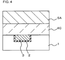
In the second porous layer forming step S2, as shown in FIG. 3, a first solution 5 is applied onto the first porous layer 4A and is then heated to form the second porous layer 5A, as shown in FIG. 4.
The first solution 5 may be the same as the first solution 4 used to form the first porous layer 4A. When the first solution 5 is applied onto the first porous layer 4A, the first solution 5 gets into the pores of the first porous layer 4A. That is, the first solution 5 gets into the pores of the first porous layer 4A to form the first porous layer 4B. Then, the applied first solution 5 is heated after the first solution 5 is infiltrated into the first porous layer 4A, preferably after a sufficient amount of time required for the first solution 5 to be completely infiltrated into the first porous layer 4A has elapsed.
After the first solution 5 is applied, it is heated at a temperature that is equal to or higher than the thermal decomposition temperature of the surfactant. In this case, the surfactant is thermally decomposed and pores are formed at the positions where there are micelles formed by the surfactant. As a result, a first porous layer 4C and a second porous layer 5A are formed (see FIG. 4).
In this case, it is possible to adjust the density of the pores in the first porous layers 4A and 4C and the second porous layer 5A according to the content of the surfactant in the first solutions 4 and 5. In this embodiment, the pore density of the first porous layer 4C is equal to 40% or below. When the pore density of the first porous layer 4C is x1%, the pore density of the first porous layer 4A and the second porous layer 5A is adjusted so as to be equal to (x1+5) % or above and preferably equal to (x1+10) % or above.
In the porous layer contracting step S3, at least one of ultraviolet rays, an electron beam, and a microwave is emitted to the first porous layer 4C and the second porous layer 5A while the first porous layer 4C and the second porous layer 5A are heated.
The heating may be performed at a temperature of equal to 100° C. or above and equal to 600° C. or below and preferably equal to 150° C. or above and equal to 450° C. or below. The ultraviolet rays with a wavelength of, for example, equal to 150 nm or above and equal to 300 nm or below may be emitted with an intensity of equal to 0.4 J/cm2 or above and equal to 20 J/cm2 or below and preferably equal to 1 J/cm2 or above and equal to 10 J/cm2 or below. The electron beam may be emitted with an energy of equal to 1 keV or above and equal to 25 keV or below and preferably equal to 10 keV or above and equal to 15 keV or below and a dose of equal to 10−3 C/cm2 or above and equal to 105 C/cm2 or below for a time equal to 10 seconds or above and equal to 10 minutes or below. The microwaves may be emitted with an energy of equal to 50 W or above and equal to 5000 W or below and preferably equal to 100 W or above and equal to 500 W or below for a time equal to 10 seconds or above and equal to 60 minutes or below and preferably equal to 10 seconds or above and equal to 10 minutes or below. In this embodiment, the heating condition and the emission condition in which the contraction ratio of each of the first porous layer 4C and the second porous layer 5A is about equal to 10% or above and equal to 40% or below may be appropriately selected.
Non-bonded portions of the SiO2 component, which is a skeleton of each of the first porous layer 4C and the second porous layer 5A, are cross-linked by the above-mentioned process to improve mechanical strength.
In the gas processing step S4, the first porous layer 4C and the second porous layer 5A are heated in an atmosphere including organic silicon compounds in gas molecules. As the gas molecule, for example, organosiloxanes, such as tetramethylcyclotetrasiloxane, octamethylcyclotetrasiloxane, hexamethyldisiloxane, or hexamethyldisilazane, or a silylation agent is used.
The heating may be performed at a temperature of equal to 150° C. or above and equal to 600° C. or below and preferably equal to 200° C. or above and equal to 450° C. or below.
This process can change a Si—OH component, which is an end group of a surface portion of each of the first porous layer 4C and the second porous layer 5A having a SiO2 component as a skeleton, into Si—H or Si—CH3, thereby reducing dielectric constant.
In the via wiring and trench wiring forming step S5, a via wiring is provided in the first porous layer and a trench wiring is buried in the second porous layer.
For example, in the first porous layer 6 and the second porous layer 7 (see FIG. 5) subjected to the steps S3 and/or S4, via hole 8 and trench 9 are formed by photolithography and etching (see FIG. 6). Then, the barrier film 12 (see FIG. 7) is formed along the side wall and the bottom of the via hole 8 and trench 9. Then, the via hole 8 and trench 9 are filled with metal and then CMP is performed. In this way, as shown in FIG. 7, the via wiring 10 can be provided in the first porous layer 6 and the trench wiring 11 can be buried in the second porous layer 7.
In the manufacturing method according to this embodiment, the same solution is applied twice (the first porous layer forming step S1 and the second porous layer forming step S2). During the second applying process, the solution is infiltrated into the previously formed porous layer (first porous layer 4A) to form a layered structure of the layers with different pore densities. In this case, it is not necessary to produce plural kinds of solutions. Therefore, it is possible to reduce manufacturing costs and improve work efficiency.
In the manufacturing method according to this embodiment, the micelle formed by the surfactant added in the solution is used as a mold of the pore. Therefore, it is possible to form a porous layer in which pores are uniformly dispersed with high density.
In the manufacturing method according to this embodiment, the porous layer contracting step S3 and/or the gas processing step S4 may be combined with each other to improve the mechanical strength of the first porous layer 6 and the second porous layer 7 and reduce dielectric constant.
In the manufacturing method according to this embodiment, it is possible to form an interlayer dielectric including a lower layer with high dielectric constant and an upper layer with low dielectric constant with the minimum number of processes. Therefore, it is possible to manufacture a multi-layer semiconductor integrated circuit device including many wiring layers at a low cost. In addition, it is possible to provide a low-k film with high mechanical strength and adhesion. Therefore, it is possible to reduce the power consumption of a circuit and improve the operation speed of the circuit. As a result, it is possible to manufacture an integrated circuit device with high reliability.
EXAMPLES
A solution (a ULKS-type application liquid manufactured by ULVAC, Inc.) including a methylsiloxane oligomer and a surfactant with a thermal decomposition temperature of 150° C. or below was applied onto a semiconductor substrate having a under layer interconnect formed thereon and then heated at 150° C. in a nitrogen atmosphere to form pores in the film. As a result, a first porous layer with a skeleton having silicon dioxide (SiO2) or silanol (SiOH) as a main component was formed.
Then, the same solution as described above was applied onto the first porous layer and then heated to 400° C. in a nitrogen atmosphere in stages. As a result, a second porous layer was formed on the first porous layer. In addition, the solution was applied onto the first porous layer and was then left for a sufficient amount of time so as to be infiltrated into the first porous layer. Then, heating was performed.
Then, ultraviolet light was emitted from a xenon excimer light source to the first porous layer and the second porous layer under the condition of 4.5 J/cm2 while heating was maintained at a temperature of 400° C. such that the first porous layer and the second porous layer were shrunk by about 10%. In addition, the layers were heated at 400° C. for 90 minutes in a tetramethylcyclotetrasiloxane vapor atmosphere. Tetramethylcyclotetrasiloxane was infiltrated into the first porous layer and the second porous layer through the pores. As a result, the amount of silanol component in the first porous layer and the second porous layer was reduced and a porous SiOCH film including silicon dioxide and methylsilicon (SiCH3) was formed.
The composition change was analyzed by a method (FTIR method) of analyzing the infrared absorption spectrum of a plurality of films with different thicknesses which was formed on the silicon substrate by the above-mentioned method. The optical characteristics of these samples were examined by a spectroscopic ellipsometry method. The examination result proved that the refractive index of the first porous layer (lower layer) was higher than that of the second porous layer (upper layer). In addition, a mercury electrode was formed on the surface of the layer to analyze capacitance with the substrate. As a result, the dielectric constant of the first porous layer (lower layer) was 2.4 and the dielectric constant of the second porous layer (upper layer) was 2.1. Since the dielectric constant of a dense silicon dioxide was 4.2, each of the first porous layer (lower layer) and the second porous layer (upper layer) is a porous low-k layer including a SiO2 skeleton. In addition, the pore density of the first porous layer and the pore density of the second porous layer calculated by Expression 1 were 38% and 48%, respectively. The Young's modulus of the first porous layer and the Young's modulus of the second porous layer measured by a nano indenter were 16 GPa and 8 GPa, respectively.
It is apparent that the present invention is not limited to the above embodiment, and may be modified and changed without departing from the scope and spirit of the invention.

Claims (7)

What is claimed is:
1. A semiconductor device comprising:
a first porous layer that is formed over a substrate and includes a SiO2 skeleton;
a second porous layer that is formed immediately above the first porous layer and includes a SiO2 skeleton;
a via wiring that is provided in the first porous layer; and
a trench wiring that is buried in the second porous layer,
wherein the first porous layer has a pore density x1 of 40% or below and the second porous layer has a pore density x2 of (x1+5) % or above.
2. A method of manufacturing a semiconductor device, the method comprising:
applying a first solution including a surfactant onto a substrate and heating the first solution to form a first porous layer;
applying the first solution onto the first porous layer and heating the first solution to form a second porous layer; and
providing a via wiring in the first porous layer and burying a trench wiring in the second porous layer after said forming the second porous layer.
3. The method of manufacturing a semiconductor device according to claim 2, wherein, in said forming the second porous layer, after the first solution is applied, the first solution is infiltrated into the first porous layer and is heated.
4. The method of manufacturing a semiconductor device according to claim 2,
wherein, when the pore density of the first porous layer after said forming the first porous layer and before said forming the second porous layer is x1,0% and the pore density of the first porous layer after said forming the second porous layer is x1,1%, x1,1 is equal to 40% or below and x1,0 is equal to (x1,1+5) % or above.
5. The method of manufacturing a semiconductor device according to claim 2,
wherein, in said forming the first porous layer and said forming the second porous layer, the heating is performed at a temperature equal to or higher than a thermal decomposition temperature of the surfactant.
6. The method of manufacturing a semiconductor device according to claim 2, further comprising:
emitting at least one of ultraviolet rays, an electron beam, and microwaves to the first porous layer and the second porous layer while performing heating after said forming the second porous layer and before said forming the via wiring and the trench wiring.
7. The method of manufacturing a semiconductor device according to claim 2, further comprising:
performing heating in an atmosphere including organic silicon in a gas molecule after said forming the second porous layer and before said forming the via wiring and the trench wiring.
US13/193,154 2010-07-29 2011-07-28 Semiconductor device and method of manufacturing semiconductor device Active 2031-12-26 US8592990B2 (en)

Applications Claiming Priority (2)

Application Number Priority Date Filing Date Title
JP2010-170099 2010-07-29
JP2010170099A JP5567926B2 (en) 2010-07-29 2010-07-29 Manufacturing method of semiconductor device

Publications (2)

Publication Number Publication Date
US20120025395A1 US20120025395A1 (en) 2012-02-02
US8592990B2 true US8592990B2 (en) 2013-11-26

Family

ID=45525910

Family Applications (1)

Application Number Title Priority Date Filing Date
US13/193,154 Active 2031-12-26 US8592990B2 (en) 2010-07-29 2011-07-28 Semiconductor device and method of manufacturing semiconductor device

Country Status (2)

Country Link
US (1) US8592990B2 (en)
JP (1) JP5567926B2 (en)

Cited By (2)

* Cited by examiner, † Cited by third party
Publication number Priority date Publication date Assignee Title
US9842804B2 (en) 2016-01-04 2017-12-12 Taiwan Semiconductor Manufacturing Company, Ltd. Methods for reducing dual damascene distortion
US11133249B2 (en) 2019-08-07 2021-09-28 Samsung Electronics Co., Ltd. Semiconductor device

Families Citing this family (2)

* Cited by examiner, † Cited by third party
Publication number Priority date Publication date Assignee Title
US9406615B2 (en) * 2013-12-24 2016-08-02 Intel Corporation Techniques for forming interconnects in porous dielectric materials
JP6728252B2 (en) * 2017-02-28 2020-07-22 株式会社東芝 Semiconductor device and manufacturing method thereof

Citations (16)

* Cited by examiner, † Cited by third party
Publication number Priority date Publication date Assignee Title
US6528409B1 (en) * 2002-04-29 2003-03-04 Advanced Micro Devices, Inc. Interconnect structure formed in porous dielectric material with minimized degradation and electromigration
US6699797B1 (en) * 2002-12-17 2004-03-02 Intel Corporation Method of fabrication of low dielectric constant porous metal silicate films
US6703324B2 (en) * 2000-12-21 2004-03-09 Intel Corporation Mechanically reinforced highly porous low dielectric constant films
US6759325B2 (en) * 2000-05-15 2004-07-06 Asm Microchemistry Oy Sealing porous structures
JP2005117026A (en) 2003-09-18 2005-04-28 Semiconductor Leading Edge Technologies Inc Method of manufacturing semiconductor device
US6958525B2 (en) * 2000-03-29 2005-10-25 Fujitsu Limited Low dielectric constant film material, film and semiconductor device using such material
US7015150B2 (en) * 2004-05-26 2006-03-21 International Business Machines Corporation Exposed pore sealing post patterning
US7018920B2 (en) * 2003-03-20 2006-03-28 Intel Corporation Composite sacrificial material
US7125794B2 (en) 2003-09-18 2006-10-24 Renesas Technology Corp. Method of manufacturing semiconductor device
US7294931B2 (en) * 2003-03-31 2007-11-13 Intel Corporation Method and apparatus for selective deposition
US7332449B2 (en) * 2005-09-30 2008-02-19 Taiwan Semiconductor Manufacturing Co., Ltd. Method for forming dual damascenes with supercritical fluid treatments
US7459398B2 (en) * 2004-08-06 2008-12-02 Kabushiki Kaisha Toshiba Slurry for CMP, polishing method and method of manufacturing semiconductor device
US7527723B2 (en) * 2004-01-16 2009-05-05 Ebara Corporation Electrolytic processing apparatus and electrolytic processing method
US7732349B2 (en) * 2004-11-30 2010-06-08 Semiconductor Energy Laboratory Co., Ltd. Manufacturing method of insulating film and semiconductor device
US7922824B2 (en) * 2005-10-05 2011-04-12 Advanced Technology Materials, Inc. Oxidizing aqueous cleaner for the removal of post-etch residues
US7972954B2 (en) * 2006-01-24 2011-07-05 Infineon Technologies Ag Porous silicon dielectric

Family Cites Families (4)

* Cited by examiner, † Cited by third party
Publication number Priority date Publication date Assignee Title
JP2004277463A (en) * 2003-03-12 2004-10-07 Fujitsu Ltd Composition for low dielectric constant film
US7696627B2 (en) * 2005-07-07 2010-04-13 Panasonic Corporation Multilayered interconnect structure and method for fabricating the same
JP5213010B2 (en) * 2007-04-13 2013-06-19 次世代半導体材料技術研究組合 Semiconductor device, manufacturing method thereof, and manufacturing device thereof
WO2009144920A1 (en) * 2008-05-29 2009-12-03 Necエレクトロニクス株式会社 Method of producing silylated porous insulating film, method of producing semiconductor device, and silylated material

Patent Citations (16)

* Cited by examiner, † Cited by third party
Publication number Priority date Publication date Assignee Title
US6958525B2 (en) * 2000-03-29 2005-10-25 Fujitsu Limited Low dielectric constant film material, film and semiconductor device using such material
US6759325B2 (en) * 2000-05-15 2004-07-06 Asm Microchemistry Oy Sealing porous structures
US6703324B2 (en) * 2000-12-21 2004-03-09 Intel Corporation Mechanically reinforced highly porous low dielectric constant films
US6528409B1 (en) * 2002-04-29 2003-03-04 Advanced Micro Devices, Inc. Interconnect structure formed in porous dielectric material with minimized degradation and electromigration
US6699797B1 (en) * 2002-12-17 2004-03-02 Intel Corporation Method of fabrication of low dielectric constant porous metal silicate films
US7018920B2 (en) * 2003-03-20 2006-03-28 Intel Corporation Composite sacrificial material
US7294931B2 (en) * 2003-03-31 2007-11-13 Intel Corporation Method and apparatus for selective deposition
US7125794B2 (en) 2003-09-18 2006-10-24 Renesas Technology Corp. Method of manufacturing semiconductor device
JP2005117026A (en) 2003-09-18 2005-04-28 Semiconductor Leading Edge Technologies Inc Method of manufacturing semiconductor device
US7527723B2 (en) * 2004-01-16 2009-05-05 Ebara Corporation Electrolytic processing apparatus and electrolytic processing method
US7015150B2 (en) * 2004-05-26 2006-03-21 International Business Machines Corporation Exposed pore sealing post patterning
US7459398B2 (en) * 2004-08-06 2008-12-02 Kabushiki Kaisha Toshiba Slurry for CMP, polishing method and method of manufacturing semiconductor device
US7732349B2 (en) * 2004-11-30 2010-06-08 Semiconductor Energy Laboratory Co., Ltd. Manufacturing method of insulating film and semiconductor device
US7332449B2 (en) * 2005-09-30 2008-02-19 Taiwan Semiconductor Manufacturing Co., Ltd. Method for forming dual damascenes with supercritical fluid treatments
US7922824B2 (en) * 2005-10-05 2011-04-12 Advanced Technology Materials, Inc. Oxidizing aqueous cleaner for the removal of post-etch residues
US7972954B2 (en) * 2006-01-24 2011-07-05 Infineon Technologies Ag Porous silicon dielectric

Non-Patent Citations (1)

* Cited by examiner, † Cited by third party
Title
N. Hata et al., "Analysis of Pore Structures in Ultra Low-k Dielectrics," Extended Abstracts of the 2002 International Conference on Solid State Devices and Materials, IEEE Electron Devices Society, Sep. 17-19, 2002, The Japan Society of Applied Physics.

Cited By (5)

* Cited by examiner, † Cited by third party
Publication number Priority date Publication date Assignee Title
US9842804B2 (en) 2016-01-04 2017-12-12 Taiwan Semiconductor Manufacturing Company, Ltd. Methods for reducing dual damascene distortion
US10332836B2 (en) 2016-01-04 2019-06-25 Taiwan Semiconductor Manufacturing Company, Ltd. Methods for reducing dual damascene distortion
US10818598B2 (en) 2016-01-04 2020-10-27 Taiwan Semiconductor Manufacturing Company, Ltd. Methods for reducing dual damascene distortion
US11482493B2 (en) 2016-01-04 2022-10-25 Taiwan Semiconductor Manufacturing Company Ltd Methods for reducing dual damascene distortion
US11133249B2 (en) 2019-08-07 2021-09-28 Samsung Electronics Co., Ltd. Semiconductor device

Also Published As

Publication number Publication date
US20120025395A1 (en) 2012-02-02
JP5567926B2 (en) 2014-08-06
JP2012033588A (en) 2012-02-16

Similar Documents

Publication Publication Date Title
JP3276963B2 (en) Method of forming dielectric film on substrate
Grill Porous pSiCOH ultralow-k dielectrics for chip interconnects prepared by PECVD
US7704872B2 (en) Ultraviolet assisted pore sealing of porous low k dielectric films
Michalak et al. Porosity scaling strategies for low-k films
Baklanov et al. Porous low dielectric constant materials for microelectronics
Morgen et al. Low dielectric constant materials for ULSI interconnects
TWI414623B (en) Low k dielectric cvd film formation process with in-situ imbedded nanolayers to improve mechanical properties
US7485582B2 (en) Hardmask for improved reliability of silicon based dielectrics
US7288292B2 (en) Ultra low k (ULK) SiCOH film and method
US8772182B2 (en) Semiconductor device having reinforced low-k insulating film and its manufacture method
TWI260684B (en) Method of manufacturing semiconductor device
Baklanov et al. Impact of VUV photons on SiO2 and organosilicate low-k dielectrics: General behavior, practical applications, and atomic models
Lionti et al. Toward successful integration of porous low-k materials: Strategies addressing plasma damage
EP0881668A2 (en) Deposition of an electrically insulating thin film with a low dielectric constant
KR20060065493A (en) Semiconductor device fabrication method
JP2008130991A (en) Semiconductor device, and manufacturing method thereof
US8592990B2 (en) Semiconductor device and method of manufacturing semiconductor device
US7830012B2 (en) Material for forming exposure light-blocking film, multilayer interconnection structure and manufacturing method thereof, and semiconductor device
Guo et al. Effects of plasma and vacuum-ultraviolet exposure on the mechanical properties of low-k porous organosilicate glass
Petkov et al. Open volume defects (measured by positron annihilation spectroscopy) in thin film hydrogen-silsesquioxane spin-on-glass; correlation with dielectric constant
US20100301495A1 (en) Semiconductor device and method for manufacturing same
JP2011082308A (en) Method of manufacturing semiconductor apparatus
US20130045337A1 (en) Homogeneous modification of porous films
JP5679662B2 (en) Dielectric cap layer
JP2006024641A (en) Semiconductor device and its manufacturing method

Legal Events

Date Code Title Description
AS Assignment

Owner name: RENESAS ELECTRONICS CORPORATION, JAPAN

Free format text: ASSIGNMENT OF ASSIGNORS INTEREST;ASSIGNORS:CHIKAKI, SHINICHI;NAKAYAMA, TAKAHIRO;SIGNING DATES FROM 20110705 TO 20110706;REEL/FRAME:026685/0643

Owner name: ULVAC, INC., JAPAN

Free format text: ASSIGNMENT OF ASSIGNORS INTEREST;ASSIGNORS:CHIKAKI, SHINICHI;NAKAYAMA, TAKAHIRO;SIGNING DATES FROM 20110705 TO 20110706;REEL/FRAME:026685/0643

STCF Information on status: patent grant

Free format text: PATENTED CASE

FPAY Fee payment

Year of fee payment: 4

AS Assignment

Owner name: RENESAS ELECTRONICS CORPORATION, JAPAN

Free format text: CHANGE OF ADDRESS;ASSIGNOR:RENESAS ELECTRONICS CORPORATION;REEL/FRAME:044928/0001

Effective date: 20150806

MAFP Maintenance fee payment

Free format text: PAYMENT OF MAINTENANCE FEE, 8TH YEAR, LARGE ENTITY (ORIGINAL EVENT CODE: M1552); ENTITY STATUS OF PATENT OWNER: LARGE ENTITY

Year of fee payment: 8